WO2012067112A1 - エピタキシャル炭化珪素単結晶基板の製造方法 - Google Patents
エピタキシャル炭化珪素単結晶基板の製造方法 Download PDFInfo
- Publication number
- WO2012067112A1 WO2012067112A1 PCT/JP2011/076303 JP2011076303W WO2012067112A1 WO 2012067112 A1 WO2012067112 A1 WO 2012067112A1 JP 2011076303 W JP2011076303 W JP 2011076303W WO 2012067112 A1 WO2012067112 A1 WO 2012067112A1
- Authority
- WO
- WIPO (PCT)
- Prior art keywords
- single crystal
- epitaxial
- silicon carbide
- crystal substrate
- carbide single
- Prior art date
- Legal status (The legal status is an assumption and is not a legal conclusion. Google has not performed a legal analysis and makes no representation as to the accuracy of the status listed.)
- Ceased
Links
Images


Classifications
-
- C—CHEMISTRY; METALLURGY
- C30—CRYSTAL GROWTH
- C30B—SINGLE-CRYSTAL GROWTH; UNIDIRECTIONAL SOLIDIFICATION OF EUTECTIC MATERIAL OR UNIDIRECTIONAL DEMIXING OF EUTECTOID MATERIAL; REFINING BY ZONE-MELTING OF MATERIAL; PRODUCTION OF A HOMOGENEOUS POLYCRYSTALLINE MATERIAL WITH DEFINED STRUCTURE; SINGLE CRYSTALS OR HOMOGENEOUS POLYCRYSTALLINE MATERIAL WITH DEFINED STRUCTURE; AFTER-TREATMENT OF SINGLE CRYSTALS OR A HOMOGENEOUS POLYCRYSTALLINE MATERIAL WITH DEFINED STRUCTURE; APPARATUS THEREFOR
- C30B29/00—Single crystals or homogeneous polycrystalline material with defined structure characterised by the material or by their shape
- C30B29/10—Inorganic compounds or compositions
- C30B29/36—Carbides
-
- H—ELECTRICITY
- H10—SEMICONDUCTOR DEVICES; ELECTRIC SOLID-STATE DEVICES NOT OTHERWISE PROVIDED FOR
- H10P—GENERIC PROCESSES OR APPARATUS FOR THE MANUFACTURE OR TREATMENT OF DEVICES COVERED BY CLASS H10
- H10P14/00—Formation of materials, e.g. in the shape of layers or pillars
- H10P14/20—Formation of materials, e.g. in the shape of layers or pillars of semiconductor materials
- H10P14/29—Formation of materials, e.g. in the shape of layers or pillars of semiconductor materials characterised by the substrates
- H10P14/2901—Materials
- H10P14/2902—Materials being Group IVA materials
- H10P14/2904—Silicon carbide
-
- C—CHEMISTRY; METALLURGY
- C30—CRYSTAL GROWTH
- C30B—SINGLE-CRYSTAL GROWTH; UNIDIRECTIONAL SOLIDIFICATION OF EUTECTIC MATERIAL OR UNIDIRECTIONAL DEMIXING OF EUTECTOID MATERIAL; REFINING BY ZONE-MELTING OF MATERIAL; PRODUCTION OF A HOMOGENEOUS POLYCRYSTALLINE MATERIAL WITH DEFINED STRUCTURE; SINGLE CRYSTALS OR HOMOGENEOUS POLYCRYSTALLINE MATERIAL WITH DEFINED STRUCTURE; AFTER-TREATMENT OF SINGLE CRYSTALS OR A HOMOGENEOUS POLYCRYSTALLINE MATERIAL WITH DEFINED STRUCTURE; APPARATUS THEREFOR
- C30B25/00—Single-crystal growth by chemical reaction of reactive gases, e.g. chemical vapour-deposition growth
- C30B25/02—Epitaxial-layer growth
- C30B25/18—Epitaxial-layer growth characterised by the substrate
- C30B25/186—Epitaxial-layer growth characterised by the substrate being specially pre-treated by, e.g. chemical or physical means
-
- C—CHEMISTRY; METALLURGY
- C30—CRYSTAL GROWTH
- C30B—SINGLE-CRYSTAL GROWTH; UNIDIRECTIONAL SOLIDIFICATION OF EUTECTIC MATERIAL OR UNIDIRECTIONAL DEMIXING OF EUTECTOID MATERIAL; REFINING BY ZONE-MELTING OF MATERIAL; PRODUCTION OF A HOMOGENEOUS POLYCRYSTALLINE MATERIAL WITH DEFINED STRUCTURE; SINGLE CRYSTALS OR HOMOGENEOUS POLYCRYSTALLINE MATERIAL WITH DEFINED STRUCTURE; AFTER-TREATMENT OF SINGLE CRYSTALS OR A HOMOGENEOUS POLYCRYSTALLINE MATERIAL WITH DEFINED STRUCTURE; APPARATUS THEREFOR
- C30B25/00—Single-crystal growth by chemical reaction of reactive gases, e.g. chemical vapour-deposition growth
- C30B25/02—Epitaxial-layer growth
- C30B25/18—Epitaxial-layer growth characterised by the substrate
- C30B25/20—Epitaxial-layer growth characterised by the substrate the substrate being of the same materials as the epitaxial layer
-
- H—ELECTRICITY
- H10—SEMICONDUCTOR DEVICES; ELECTRIC SOLID-STATE DEVICES NOT OTHERWISE PROVIDED FOR
- H10P—GENERIC PROCESSES OR APPARATUS FOR THE MANUFACTURE OR TREATMENT OF DEVICES COVERED BY CLASS H10
- H10P14/00—Formation of materials, e.g. in the shape of layers or pillars
- H10P14/20—Formation of materials, e.g. in the shape of layers or pillars of semiconductor materials
- H10P14/24—Formation of materials, e.g. in the shape of layers or pillars of semiconductor materials using chemical vapour deposition [CVD]
-
- H—ELECTRICITY
- H10—SEMICONDUCTOR DEVICES; ELECTRIC SOLID-STATE DEVICES NOT OTHERWISE PROVIDED FOR
- H10P—GENERIC PROCESSES OR APPARATUS FOR THE MANUFACTURE OR TREATMENT OF DEVICES COVERED BY CLASS H10
- H10P14/00—Formation of materials, e.g. in the shape of layers or pillars
- H10P14/20—Formation of materials, e.g. in the shape of layers or pillars of semiconductor materials
- H10P14/29—Formation of materials, e.g. in the shape of layers or pillars of semiconductor materials characterised by the substrates
- H10P14/2926—Crystal orientations
-
- H—ELECTRICITY
- H10—SEMICONDUCTOR DEVICES; ELECTRIC SOLID-STATE DEVICES NOT OTHERWISE PROVIDED FOR
- H10P—GENERIC PROCESSES OR APPARATUS FOR THE MANUFACTURE OR TREATMENT OF DEVICES COVERED BY CLASS H10
- H10P14/00—Formation of materials, e.g. in the shape of layers or pillars
- H10P14/20—Formation of materials, e.g. in the shape of layers or pillars of semiconductor materials
- H10P14/34—Deposited materials, e.g. layers
- H10P14/3402—Deposited materials, e.g. layers characterised by the chemical composition
- H10P14/3404—Deposited materials, e.g. layers characterised by the chemical composition being Group IVA materials
- H10P14/3408—Silicon carbide
-
- H—ELECTRICITY
- H10—SEMICONDUCTOR DEVICES; ELECTRIC SOLID-STATE DEVICES NOT OTHERWISE PROVIDED FOR
- H10P—GENERIC PROCESSES OR APPARATUS FOR THE MANUFACTURE OR TREATMENT OF DEVICES COVERED BY CLASS H10
- H10P14/00—Formation of materials, e.g. in the shape of layers or pillars
- H10P14/20—Formation of materials, e.g. in the shape of layers or pillars of semiconductor materials
- H10P14/36—Formation of materials, e.g. in the shape of layers or pillars of semiconductor materials characterised by treatments done before the formation of the materials
-
- Y—GENERAL TAGGING OF NEW TECHNOLOGICAL DEVELOPMENTS; GENERAL TAGGING OF CROSS-SECTIONAL TECHNOLOGIES SPANNING OVER SEVERAL SECTIONS OF THE IPC; TECHNICAL SUBJECTS COVERED BY FORMER USPC CROSS-REFERENCE ART COLLECTIONS [XRACs] AND DIGESTS
- Y10—TECHNICAL SUBJECTS COVERED BY FORMER USPC
- Y10S—TECHNICAL SUBJECTS COVERED BY FORMER USPC CROSS-REFERENCE ART COLLECTIONS [XRACs] AND DIGESTS
- Y10S438/00—Semiconductor device manufacturing: process
- Y10S438/931—Silicon carbide semiconductor
Definitions
- the present invention relates to a method for manufacturing an epitaxial silicon carbide (SiC) single crystal substrate.
- SiC Silicon carbide
- a SiC thin film is epitaxially grown on the substrate by a method called thermal CVD (thermochemical vapor deposition) or ion implantation is usually performed.
- thermal CVD thermal chemical vapor deposition
- ion implantation ion implantation
- the dopant is directly implanted by the method, but in the latter case, annealing at a high temperature is required after implantation, and therefore, thin film formation by epitaxial growth is frequently used.
- the diameters of SiC substrates are mainly 3 inches and 4 inches (76 mm and 100 mm), so that epitaxial growth is also performed on such substrates, but the defect density such as basal plane dislocation is reduced, and From the standpoint of increasing the yield of the substrate from the SiC ingot, the off-angle of the substrate is about 4 ° to less than the conventional 8 °.
- the ratio of the number of carbon atoms to the number of silicon atoms (C / Si ratio) in the material gas that flows during growth is generally lower than before. .
- Non-Patent Document 1 discloses that epitaxial growth is performed after pretreatment etching in an atmosphere of hydrogen, hydrogen + propane, hydrogen + silane on a 4 ° off SiC substrate, and hydrogen + silane pretreatment etching is performed. This shows that the surface state of the epitaxial film has been improved as compared with the prior art.
- Patent Document 1 describes that during epitaxial growth, hydrogen chloride (HCl) is included in the carrier gas of the reaction gas, and chlorine (Cl) is included in the silicon (Si) source gas.
- Patent Document 1 does not relate to pretreatment for epitaxial growth.
- Patent Document 2 relates to a method for producing a SiC single crystal wafer. Before CVD growth, surface treatment (for example, chemical mechanical polishing, hydrogen etching, etc.) of the substrate surface is performed, and the temperature is raised or lowered. It describes that the substrate surface is etched. However, specific conditions regarding etching are not disclosed.
- surface treatment for example, chemical mechanical polishing, hydrogen etching, etc.
- Patent Document 3 relates to etching a surface of a substrate by an in situ deposition process.
- the problem of Patent Document 3 is that an etching chemical (HCl, Cl 2 , HF, HBr, etc.) and a deposition process gas containing silicon and hydrogen are used together except for limited conditions due to safety issues. Is not possible or is incompatible.
- a hydrogen-containing gas and an etching chemical are reacted to form a metastable chemical species adjacent to the surface of the wafer.
- Various metastable chemical species are produced that vary significantly in the growth and etching reaction pathways, each of which is described as having a short lifetime.
- specific conditions that can realize high-quality epitaxial growth are not disclosed.
- the substrate surface may be adversely affected.
- an object of the present invention is to provide a method for manufacturing an epitaxial SiC single crystal substrate having a high-quality epitaxial film having an excellent surface state.
- the present invention has been found and completed by forming an epitaxial layer after performing pretreatment etching by flowing a gas containing silicon and chlorine together with hydrogen gas before epitaxial growth. is there. That is, the present invention (1) A method of manufacturing an epitaxial silicon carbide single crystal substrate by epitaxially growing silicon carbide on a silicon carbide single crystal substrate, wherein pretreatment is performed by flowing a gas containing silicon and chlorine together with hydrogen gas before epitaxial growth.
- An epitaxial silicon carbide single crystal substrate manufacturing method wherein an epitaxial layer is formed after etching; (2) The epitaxial carbonization according to (1), wherein in the pretreatment etching, a concentration of silicon atoms in a gas containing silicon and chlorine with respect to hydrogen atoms in hydrogen gas is 0.0001% or more and 0.01% or less. Manufacturing method of silicon single crystal substrate, (3) The epitaxial carbonization according to (1), wherein in the pretreatment etching, a concentration of chlorine atoms in a gas containing silicon and chlorine with respect to hydrogen atoms in hydrogen gas is 0.0001% or more and 0.1% or less.
- Manufacturing method of silicon single crystal substrate (4) The epitaxial silicon carbide single crystal substrate according to (1), wherein a gas containing silicon and chlorine used for the pretreatment etching is SiH n Cl 4-n (where n is an integer of 0 to 3).
- Production method (5) The method for manufacturing an epitaxial silicon carbide single crystal substrate according to (1), wherein the pretreatment etching is performed at a temperature of 1550 ° C. or higher and 1650 ° C. or lower.
- the present invention it is possible to provide a SiC single crystal substrate having a high-quality epitaxial film with an excellent surface state in an epitaxial film on a substrate having an off angle of about 4 ° or less.
- the device using the epitaxial SiC single crystal substrate of the present invention is formed on a high-quality epitaxial film having an excellent surface state, its characteristics and yield are improved.
- Diagram showing typical growth sequence when performing conventional epitaxial growth The figure which shows the growth sequence at the time of performing epitaxial growth by one method of this invention Optical micrograph showing the surface state of a film epitaxially grown by one method of the present invention Optical micrograph showing the surface state of a film epitaxially grown by a conventional method
- the apparatus suitably used for epitaxial growth in the present invention may be a horizontal CVD apparatus.
- the CVD method has a simple apparatus configuration and can control growth by turning gas on / off. Therefore, the CVD method is a growth method with excellent controllability and reproducibility of the epitaxial film.
- epitaxial growth can also be performed by a molecular beam epitaxy method (MBE method), a liquid phase epitaxy method (LPE method), or the like.
- FIG. 1 shows a typical growth sequence in performing conventional epitaxial film growth together with gas introduction timing.
- a substrate is set in a growth furnace, the inside of the growth furnace is evacuated, and hydrogen gas is introduced to adjust the pressure to 1 ⁇ 10 4 to 3 ⁇ 10 4 Pa.
- the temperature of the growth furnace is raised while keeping the pressure constant, and after reaching the growth temperature of 1550 to 1650 ° C., the material gases SiH 4 and C 2 H 4 and the doping gas N 2 are introduced.
- SiH 4 flow rate per minute 40 ⁇ 50cm 3 C 2 H 4 flow rate per minute 20 ⁇ 40 cm 3
- the growth rate is per hour 6 ⁇ 7 [mu] m.
- This growth rate is determined in consideration of productivity because the film thickness of the normally used epitaxial layer is about 10 ⁇ m.
- the introduction of SiH 4 , C 2 H 4 and N 2 is stopped, and the temperature is lowered with only hydrogen gas flowing. After the temperature has dropped to room temperature, the introduction of hydrogen gas is stopped, the growth chamber is evacuated, an inert gas is introduced into the growth chamber, the growth chamber is returned to atmospheric pressure, and the substrate is taken out.
- there is no particular pre-treatment etching step but etching treatment in hydrogen gas is inevitably performed until the growth temperature is reached in hydrogen gas. Will be.
- a SiC single crystal substrate is set, the inside of the growth furnace is evacuated, hydrogen gas is introduced, and the pressure is adjusted to 1 ⁇ 10 4 to 3 ⁇ 10 4 Pa. Thereafter, the temperature of the growth furnace is raised while keeping the pressure constant, and when the temperature reaches 1550 to 1650 ° C., SiH n Cl 4-n gas (where n is an integer of 0 to 3) is introduced. At this time, the amount of SiH n Cl 4-n gas introduced is preferably 0.3 cm 3 / min to 30 cm 3 / min, preferably 3 cm 3 / min from the viewpoint of obtaining a good surface state before growth.
- the amount of hydrogen gas introduced is preferably from 100 L / min to 200 L / min, and preferably from 140 L / min to 160 L / min.
- the introduction of SiH n Cl 4-n gas is stopped, and SiH 4 and C 2 H 4 as material gases and N 2 as a doping gas are introduced to grow.
- the subsequent procedure is the same as in FIG.
- SiH n Cl 4-n gas examples include silicon tetrachloride (SiCl 4 ), trichlorosilane (SiHCl 3 ), dichlorosilane (SiH 2 Cl 2 ), and chlorosilane (SiH 3 Cl). These may be used alone or in combination of two or more.
- the type of material gas is not particularly limited, and in addition to monosilane and ethylene as described above, disilane, dichlorosilane, trichlorosilane, etc. may be used as the silicon source gas, and propane, methane may be used as the carbon source gas. , Ethane, acetylene or the like may be used.
- the surface state in the subsequent epitaxial growth film is pre-growth etching using silane. It will be better than the case. This is considered as follows. In the case of silane, when it decomposes, many types of compounds with the shape of Si x H y are generated, and it is considered that the etching state is determined by their ratio, so the etching rate and the surface state after etching are highly reproducible. It seems difficult to control.
- Patent Document 1 discloses that hydrogen chloride (HCl) is included in a carrier gas used for epitaxial growth, and chlorine (Cl) is included in a silicon (Si) source gas.
- etching of an epitaxial film with contained chlorine or promotion of decomposition of Si source gas with chlorine is described.
- the purpose is to improve the uniformity of the thickness and doping density of the epitaxial film, and by supplying in the form of SiCl 2 , which is the purpose of the SiH n Cl 4-n gas and the like in the present invention, it is stable.
- the effect is fundamentally different from achieving an etching rate and an Si-rich etching state, thereby realizing an optimal pre-epitaxial growth state.
- an epitaxial film having an excellent surface state can be obtained in an epitaxial film on a substrate having an off angle of about 4 ° or less.
- the amount of SiH n Cl 4-n gas or the like can be reduced. Since etching will not be performed sufficiently if there is little, there exists a minimum in the flow volume. Further, if the amount of SiH n Cl 4-n gas is excessively increased, growth starts and an unnecessary epitaxial film may be formed.
- the concentration of silicon atoms in a gas containing silicon and chlorine such as SiH n Cl 4-n gas with respect to hydrogen atoms in hydrogen gas is preferably 0.0001% or more and 0.01% or less, and more preferably 0.001% or more and 0.01% or less.
- the concentration of chlorine atoms in the gas containing silicon and chlorine, such as SiH n Cl 4-n gas, with respect to hydrogen atoms in the hydrogen gas is 0.0001% or more and 0.0. It is preferably 1% or less, and more preferably 0.001% or more and 0.1% or less.
- the temperature during the pretreatment etching is preferably 1550 ° C. or higher and 1650 ° C. or lower.
- Etching is preferably performed in the range of 1 ⁇ m or more and 1 ⁇ m or less, and more preferably 0.3 ⁇ m or more and 0.6 ⁇ m or less.
- the present invention is particularly effective in forming an epitaxial film on a SiC substrate having an off angle of 4 ° or less.
- the present invention is naturally applicable to a substrate having an off angle exceeding 4 °. It has the effect.
- the lower limit of the off angle is 0 °.
- Devices suitably formed on the epitaxial SiC single crystal substrate grown in this way are devices used for power control, such as Schottky barrier diodes, PIN diodes, MOS diodes, MOS transistors, and the like.
- Example 1 From a SiC single crystal ingot for a 3-inch (76 mm) wafer, sliced at a thickness of about 400 ⁇ m, and subjected to normal grinding with rough cutting and diamond abrasive grains, on the Si surface of a SiC single crystal substrate having a 4H type polytype, Epitaxial growth was performed. The off angle of the substrate is 4 °.
- a substrate was set in a growth furnace, the inside of the growth furnace was evacuated, and then the pressure was adjusted to 1.0 ⁇ 10 4 Pa while introducing 150 L of hydrogen gas per minute. Thereafter, the temperature of the growth furnace is raised to 1600 ° C.
- trichlorosilane SiHCl 3
- concentration of silicon atoms and chlorine atoms in trichlorosilane with respect to hydrogen atoms in hydrogen gas is 0.001% and 0.003%
- pretreatment etching was performed by about 0.5 ⁇ m.
- the introduction of trichlorosilane was stopped, the SiH 4 flow rate was 40 cm 3 / min, the C 2 H 4 flow rate was 22 cm 3 / min (C / Si ratio 1.1), and the N 2 flow rate of doping gas was 1 cm / min.
- the epitaxial layer was grown to about 10 ⁇ m.
- the SiC single crystal substrate etching amount by pretreatment etching an experiment in which only the pretreatment etching of the epitaxial film is performed in advance is performed, and the film thickness before and after the etching is determined by the FT-IR method (for example, Nanometrics FTIR apparatus) It is a value calculated by measuring with the above.
- the FT-IR method for example, Nanometrics FTIR apparatus
- FIG. 3 shows an optical micrograph (for example, a differential interference image using an Olympus MX61 microscope) of the film epitaxially grown in this way.
- FIG. 3 shows that a good film with less surface roughness and defects is obtained.
- the Ra value of the surface roughness (arithmetic average surface roughness: JIS) B0601-1994) was excellent at 0.20 nm and flatness.
- Example 2 Epitaxial growth was performed on the Si surface of a 3 inch (76 mm) SiC single crystal substrate having a 4H-type polytype, which was sliced, roughly ground, and normally polished in the same manner as in Example 1. The off angle of the substrate is 4 °.
- the procedure up to the start of the growth pretreatment, temperature, introduction of hydrogen gas, etc. are the same as in Example 1. After reaching 1600 ° C., 6 cm 3 of dichlorosilane (SiH 2 Cl 2 ) per minute (in hydrogen gas)
- the concentration of silicon atoms and chlorine atoms in dichlorosilane with respect to hydrogen atoms was 0.002% and 0.004%, respectively, and pretreatment etching was performed at about 0.5 ⁇ m.
- the epitaxial layer was grown to about 10 ⁇ m.
- the film epitaxially grown in this way was a good film with less surface roughness and defects, and the surface roughness Ra value was excellent at 0.22 nm and flatness.
- Example 3 Epitaxial growth was performed on the Si surface of a 3 inch (76 mm) SiC single crystal substrate having a 4H-type polytype, which was sliced, roughly ground, and normally polished in the same manner as in Example 1. The off angle of the substrate is 4 °.
- the procedure up to the start of the growth pretreatment, temperature, introduction of hydrogen gas, etc. are the same as in Example 1. After reaching 1600 ° C., 20 cm 3 of chlorosilane (SiH 3 Cl) per minute (hydrogen atoms in hydrogen gas) The concentration of silicon atoms and chlorine atoms in chlorosilane was 0.007%, respectively, and pre-treatment etching was performed at about 0.6 ⁇ m.
- Example 4 Epitaxial growth was performed on the Si surface of a 3 inch (76 mm) SiC single crystal substrate having a 4H-type polytype, which was sliced, roughly ground, and normally polished in the same manner as in Example 1. The off angle of the substrate is 4 °.
- the procedure up to the start of the growth pretreatment, temperature, introduction of hydrogen gas, and the like are the same as in Example 1. After reaching 1550 ° C., 6 cm 3 of dichlorosilane (SiH 2 Cl 2 ) per minute (in hydrogen gas)
- the concentration of silicon atoms and chlorine atoms in dichlorosilane with respect to hydrogen atoms was 0.002% and 0.004%, respectively, and pretreatment etching was performed at about 0.5 ⁇ m.
- the epitaxial layer was grown to about 10 ⁇ m.
- the film epitaxially grown in this way was a good film with less surface roughness and defects, and the surface roughness Ra value was excellent at 0.23 nm and flatness.
- Example 5 Epitaxial growth was performed on the Si surface of a 3 inch (76 mm) SiC single crystal substrate having a 4H-type polytype, which was sliced, roughly ground, and normally polished in the same manner as in Example 1. The off angle of the substrate is 4 °. The procedure up to the start of the growth pretreatment, the temperature, the introduction of hydrogen gas, and the like are the same as in Example 1. After reaching 1650 ° C., trichlorosilane (SiHCl 3 ) was added at 3 cm 3 per minute (hydrogen atoms in hydrogen gas).
- SiHCl 3 trichlorosilane
- the concentration of silicon atoms and chlorine atoms in trichlorosilane was 0.001% and 0.003%, respectively, and pretreatment etching was performed at about 0.6 ⁇ m. Thereafter, the introduction of trichlorosilane was stopped, the SiH 4 flow rate was 40 cm 3 / min, the C 2 H 4 flow rate was 22 cm 3 / min (C / Si ratio 1.1), and the N 2 flow rate of doping gas was 1 cm / min.
- the epitaxial layer was grown to about 10 ⁇ m. The film epitaxially grown in this way was a good film with less surface roughness and defects, and the surface roughness Ra value was excellent at 0.21 nm and flatness.
- Example 6 Epitaxial growth was performed on the Si surface of a 3 inch (76 mm) SiC single crystal substrate having a 4H-type polytype, which was sliced, roughly ground, and normally polished in the same manner as in Example 1. The off angle of the substrate is 4 °. The procedure up to the start of the growth pretreatment, temperature, introduction of hydrogen gas, and the like are the same as in Example 1.
- silane (SiH 4 ) per minute relative to the hydrogen atoms in the hydrogen gas
- concentration of silicon atoms in silane is 0.007%
- hydrogen chloride (HCl) is introduced at 60 cm 3 / min (the concentration of chlorine atoms in hydrogen chloride relative to the hydrogen atoms in hydrogen gas is 0.02%)
- Pretreatment etching was performed at about 0.5 ⁇ m.
- the epitaxial layer was grown to about 10 ⁇ m at a rate of 1 cm 3 .
- the film epitaxially grown in this way was a good film with less surface roughness and defects, and the surface roughness Ra value was 0.55 nm, which was excellent in flatness.
- Example 7 Epitaxial growth was performed on the Si surface of a 3 inch (76 mm) SiC single crystal substrate having a 4H-type polytype, which was sliced, roughly ground, and normally polished in the same manner as in Example 1. The off angle of the substrate is 4 °.
- the procedure up to the start of the growth pretreatment, the temperature, the introduction of hydrogen gas, etc. are the same as in Example 1.
- trichlorosilane (SiHCl 3 ) was added at 3 cm 3 / min (hydrogen atoms in hydrogen gas).
- concentration of silicon atoms and chlorine atoms in trichlorosilane was 0.001% and 0.003%, respectively, and pretreatment etching was performed at about 1.0 ⁇ m.
- the epitaxial layer was grown to about 10 ⁇ m.
- the film epitaxially grown in this way was a good film with less surface roughness and defects, and the surface roughness Ra value was 0.48 nm and was excellent in flatness.
- Example 8 Epitaxial growth was performed on the Si surface of a 3 inch (76 mm) SiC single crystal substrate having a 4H-type polytype, which was sliced, roughly ground, and normally polished in the same manner as in Example 1. The off angle of the substrate is 6 °. The procedure up to the start of the growth pretreatment, temperature, introduction of hydrogen gas, and the like are the same as in Example 1. After reaching 1600 ° C., trichlorosilane (SiHCl 3 ) was added at 3 cm 3 per minute (hydrogen atoms in hydrogen gas). The concentration of silicon atoms and chlorine atoms in trichlorosilane was 0.001% and 0.003%, respectively, and pretreatment etching was performed at about 0.5 ⁇ m.
- SiHCl 3 trichlorosilane
- the introduction of trichlorosilane was stopped, the SiH 4 flow rate was 40 cm 3 / min, the C 2 H 4 flow rate was 20 cm 3 / min (C / Si ratio 1.0), and the N 2 flow rate as a doping gas was 1 cm / min.
- the epitaxial layer was grown to about 10 ⁇ m. The film epitaxially grown in this way was a good film with less surface roughness and defects, and the surface roughness Ra value was excellent at 0.21 nm and flatness.
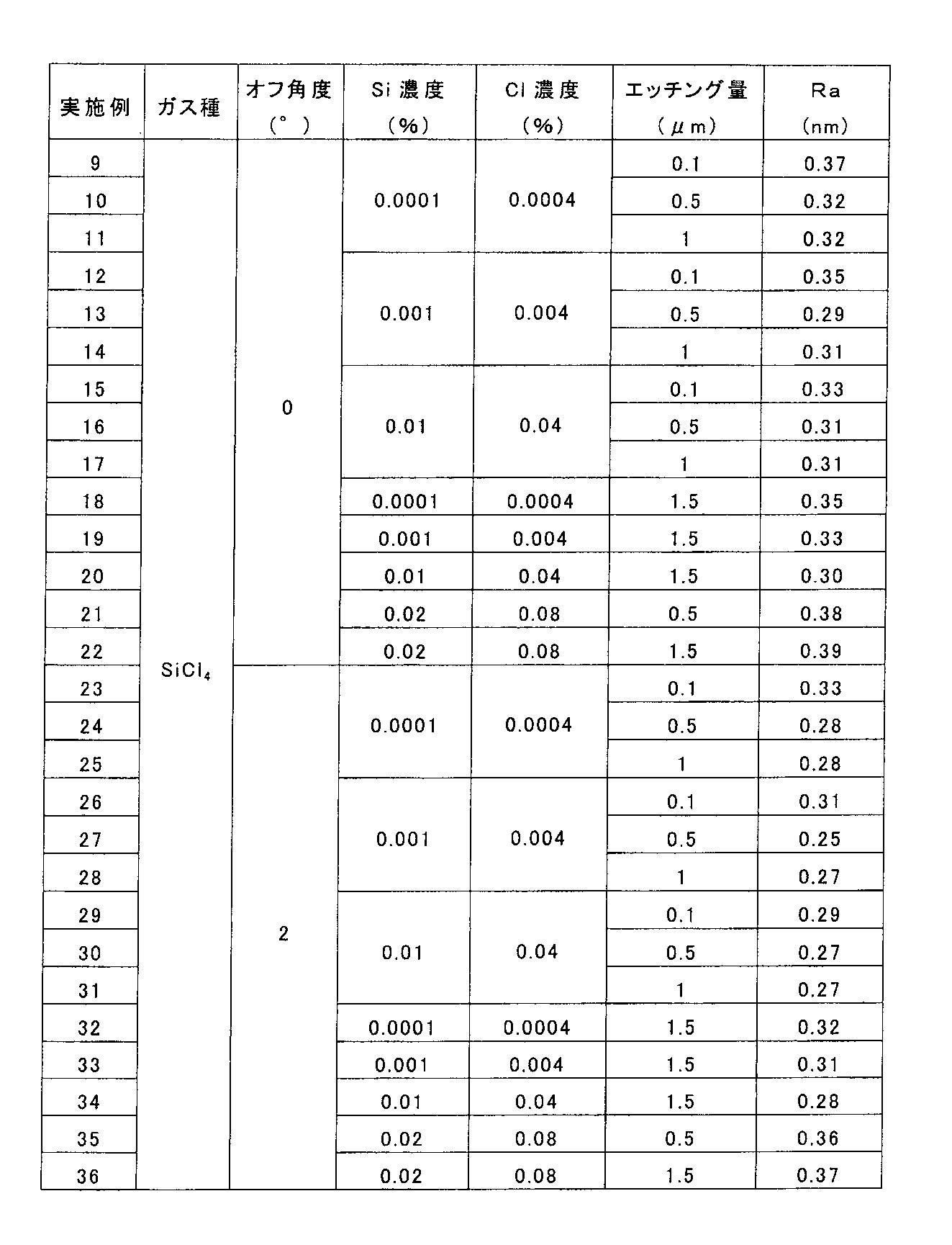
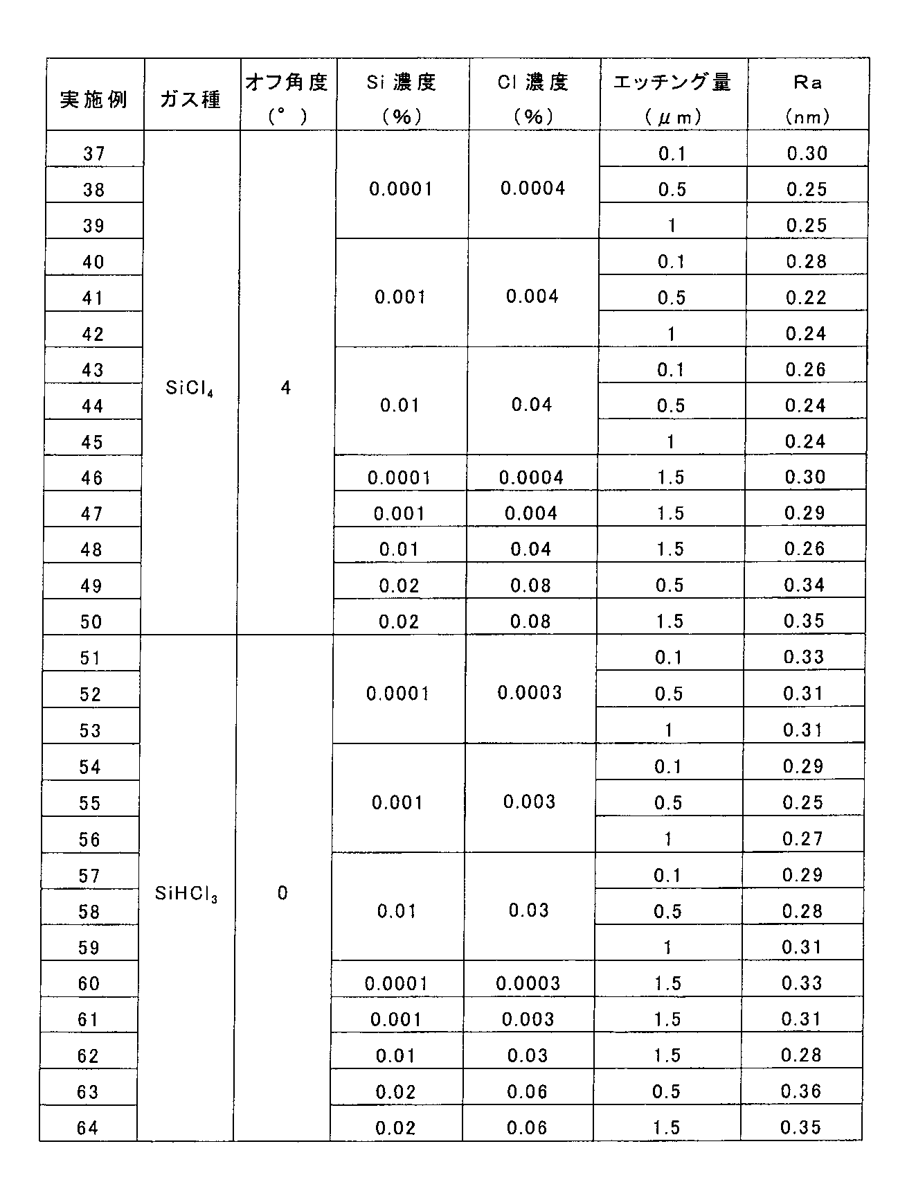
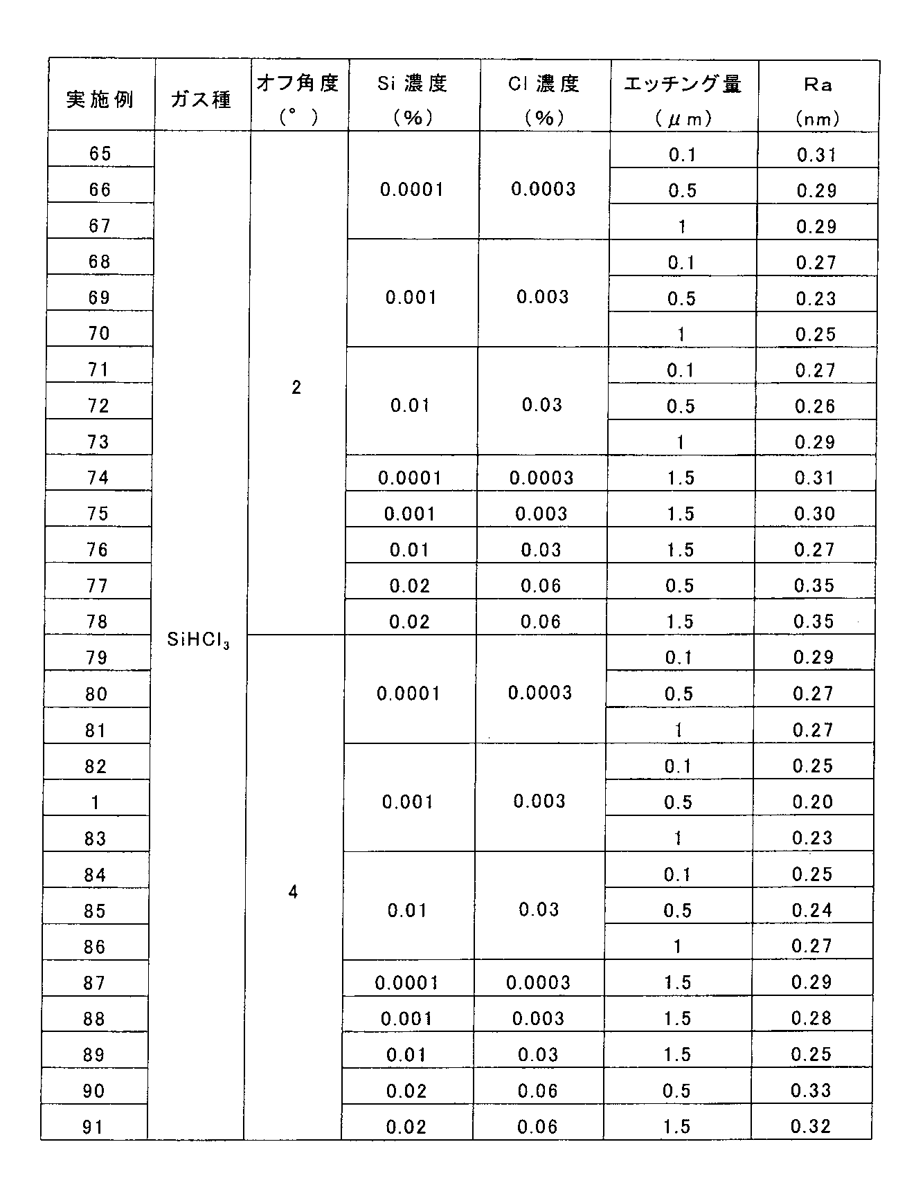
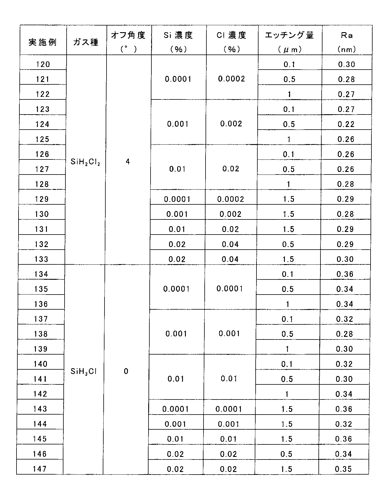
- Example 9 Epitaxial growth was performed on the Si surface of a 3 inch (76 mm) SiC single crystal substrate having a 4H-type polytype, which was sliced, roughly ground, and normally polished in the same manner as in Example 1. Procedures up growth prior to start of treatment, temperature, introduction of hydrogen gas is the same as in Example 1, Table off angle of the substrate, the pretreatment etching amount, the gas species and the concentration of SiH n Cl 4-n gas 1 to Table 6 have been changed.
- the epitaxial layer was grown about 10 ⁇ m at a certain N 2 flow rate of 1 cm 3 per minute.
- the film epitaxially grown in this way is a good film with less surface roughness and defects, and the Ra value of the surface roughness is small as shown in Tables 1 to 6.
- the concentration (%) in the table represents the concentration of silicon atoms (Si concentration) and the concentration of chlorine atoms (Cl concentration) in SiH n Cl 4-n gas with respect to hydrogen atoms in hydrogen gas.
- Example 1 Epitaxial growth was performed on the Si surface of a 3 inch (76 mm) SiC single crystal substrate having a 4H-type polytype, which was sliced, roughly ground, and normally polished in the same manner as in Example 1.
- the off angle of the substrate is 4 °.
- the procedure up to the start of the growth pretreatment, the temperature, the introduction of hydrogen gas, and the like are the same as in Example 1. However, pretreatment etching in which a gas containing silicon and chlorine is passed is not performed, and the SiH 4 flow rate is 40 cm 3 / min.
- the epitaxial layer was grown to a thickness of about 10 ⁇ m with a C 2 H 4 flow rate of 22 cm 3 / min (C / Si ratio 1.1) and a N 2 flow rate of doping gas of 1 cm 3 / min.
- FIG. 4 shows an optical micrograph of the film thus epitaxially grown.
- FIG. 4 shows that the film has many triangular defects and a large surface roughness, and the Ra value of the surface roughness was as large as 1.5 nm.
- the SiH 4 flow rate is 40 cm 3 / min
- the C 2 H 4 flow rate is 22 cm 3 / min (C / Si ratio 1.1)
- the N 2 flow rate of doping gas is 1 cm 3 / min
- the epitaxial layer is reduced to about Grows 10 ⁇ m.
- the film epitaxially grown in this way many defects and pits that are thought to be caused by instability of pretreatment etching or Si droplets are observed as in FIG. 4, and the Ra value of the surface roughness is 1.1 nm. And showed a large value.
- the present invention it is possible to stably produce an epitaxial SiC single crystal substrate having a high quality epitaxial film with a good surface state in epitaxial growth on the SiC single crystal substrate. Therefore, if an electronic device is formed on such a substrate, it can be expected that the characteristics and yield of the device are improved.
Landscapes
- Chemical & Material Sciences (AREA)
- Crystallography & Structural Chemistry (AREA)
- Engineering & Computer Science (AREA)
- Materials Engineering (AREA)
- Metallurgy (AREA)
- Organic Chemistry (AREA)
- Chemical Kinetics & Catalysis (AREA)
- General Chemical & Material Sciences (AREA)
- Inorganic Chemistry (AREA)
- Crystals, And After-Treatments Of Crystals (AREA)
- Chemical Vapour Deposition (AREA)
Abstract
Description
(1) 炭化珪素単結晶基板上に炭化珪素をエピタキシャル成長してエピタキシャル炭化珪素単結晶基板を製造する方法であって、エピタキシャル成長を行なう前に、水素ガスと共に珪素と塩素を含むガスを流して前処理エッチングを行なった後に、エピタキシャル層を形成することを特徴とするエピタキシャル炭化珪素単結晶基板の製造方法、
(2) 前記前処理エッチングにおいて、水素ガス中の水素原子に対する珪素と塩素を含むガス中の珪素原子の濃度が、0.0001%以上0.01%以下である(1)に記載のエピタキシャル炭化珪素単結晶基板の製造方法、
(3) 前記前処理エッチングにおいて、水素ガス中の水素原子に対する珪素と塩素を含むガス中の塩素原子の濃度が、0.0001%以上0.1%以下である(1)に記載のエピタキシャル炭化珪素単結晶基板の製造方法、
(4) 前記前処理エッチングに用いる珪素と塩素を含むガスが、SiHnCl4-n(式中、nは0~3の整数)である(1)に記載のエピタキシャル炭化珪素単結晶基板の製造方法、
(5) 前記前処理エッチングを、1550℃以上1650℃以下の温度で実施する(1)に記載のエピタキシャル炭化珪素単結晶基板の製造方法、
(6) 前記前処理エッチングにおいて、エッチング量が0.1μm以上1μm以下である(1)に記載のエピタキシャル炭化珪素単結晶基板の製造方法、
(7) 前記エピタキシャル成長が、熱化学蒸着法(CVD法)である(1)に記載のエピタキシャル炭化珪素単結晶基板の製造方法、
(8) 前記炭化珪素単結晶基板のオフ角度が4°以下である(1)に記載のエピタキシャル炭化珪素単結晶基板の製造方法、である。
まず、SiC単結晶基板上へのエピタキシャル成長について述べる。
本発明で好適にエピタキシャル成長に用いる装置は、横型のCVD装置であってもよい。CVD法は、装置構成が簡単であり、ガスのon/offで成長を制御できるため、エピタキシャル膜の制御性、再現性に優れた成長方法である。また、CVD法以外に、分子線エピタキシー法(MBE法)、液相エピタキシー法(LPE法)等によって、エピタキシャル成長を行なうこともできる。
3インチ(76mm)ウェーハ用SiC単結晶インゴットから、約400μmの厚さでスライスし、粗削りとダイヤモンド砥粒による通常研磨を実施した、4H型のポリタイプを有するSiC単結晶基板のSi面に、エピタキシャル成長を実施した。基板のオフ角は4°である。成長の手順としては、成長炉に基板をセットし、成長炉内を真空排気した後、水素ガスを毎分150L導入しながら圧力を1.0×10⁴Paに調整した。その後、圧力を一定に保ちながら成長炉の温度を1600℃まで上げ、トリクロロシラン(SiHCl3)を毎分3cm3(水素ガス中の水素原子に対するトリクロロシラン中の珪素原子と塩素原子の濃度はそれぞれ0.001%と0.003%)導入して、前処理エッチングを約0.5μm行なった。その後、トリクロロシランの導入を止め、SiH4流量を毎分40cm3、C2H4流量を毎分22cm3(C/Si比1.1)、さらにドーピングガスであるN2流量を毎分1cm3にしてエピタキシャル層を約10μm成長した。なお、前処理エッチングによるSiC単結晶基板のエッチング量は、事前にエピタキシャル膜の前処理エッチングのみを行う実験を実施し、エッチング前後での膜厚をFT-IR法(例えばナノメトリクス社FTIR装置)等で測定して算出した値である。
実施例1と同様にスライス、粗削り、通常研磨を行った、4H型のポリタイプを有する3インチ(76mm)のSiC単結晶基板のSi面に、エピタキシャル成長を実施した。基板のオフ角は4°である。成長前処理開始までの手順、温度、水素ガスの導入等は、実施例1と同様であり、1600℃に達した後に、ジクロロシラン(SiH2Cl2)を毎分6cm3(水素ガス中の水素原子に対するジクロロシラン中の珪素原子と塩素原子の濃度はそれぞれ0.002%と0.004%)導入して、前処理エッチングを約0.5μm行なった。その後、ジクロロシランの導入を止め、SiH4流量を毎分40cm3、C2H4流量を毎分20cm3(C/Si比1.0)、さらにドーピングガスであるN2流量を毎分1cm3にしてエピタキシャル層を約10μm成長した。このようにしてエピタキシャル成長を行った膜は、表面荒れや欠陥の少ない良好な膜であり、表面粗さのRa値は0.22nmと平坦性に優れていた。
実施例1と同様にスライス、粗削り、通常研磨を行った、4H型のポリタイプを有する3インチ(76mm)のSiC単結晶基板のSi面に、エピタキシャル成長を実施した。基板のオフ角は4°である。成長前処理開始までの手順、温度、水素ガスの導入等は、実施例1と同様であり、1600℃に達した後に、クロロシラン(SiH3Cl)を毎分20cm3(水素ガス中の水素原子に対するクロロシラン中の珪素原子と塩素原子の濃度はそれぞれ0.007%)導入して、前処理エッチングを約0.6μm行なった。その後、クロロシランの導入を止め、SiH4流量を毎分40cm3、C2H4流量を毎分16cm3(C/Si比0.8)、さらにドーピングガスであるN2流量を毎分1cm3にしてエピタキシャル層を約10μm成長した。このようにしてエピタキシャル成長を行った膜は、表面荒れや欠陥の少ない良好な膜であり、表面粗さのRa値は0.25nmと平坦性に優れていた。
実施例1と同様にスライス、粗削り、通常研磨を行った、4H型のポリタイプを有する3インチ(76mm)のSiC単結晶基板のSi面に、エピタキシャル成長を実施した。基板のオフ角は4°である。成長前処理開始までの手順、温度、水素ガスの導入等は、実施例1と同様であり、1550℃に達した後に、ジクロロシラン(SiH2Cl2)を毎分6cm3(水素ガス中の水素原子に対するジクロロシラン中の珪素原子と塩素原子の濃度はそれぞれ0.002%と0.004%)導入して、前処理エッチングを約0.5μm行なった。その後、ジクロロシランの導入を止め、SiH4流量を毎分40cm3、C2H4流量を毎分20cm3(C/Si比1.0)、さらにドーピングガスであるN2流量を毎分1cm3にしてエピタキシャル層を約10μm成長した。このようにしてエピタキシャル成長を行った膜は、表面荒れや欠陥の少ない良好な膜であり、表面粗さのRa値は0.23nmと平坦性に優れていた。
実施例1と同様にスライス、粗削り、通常研磨を行った、4H型のポリタイプを有する3インチ(76mm)のSiC単結晶基板のSi面に、エピタキシャル成長を実施した。基板のオフ角は4°である。成長前処理開始までの手順、温度、水素ガスの導入等は、実施例1と同様であり、1650℃に達した後に、トリクロロシラン(SiHCl3)を毎分3cm3(水素ガス中の水素原子に対するトリロロシラン中の珪素原子と塩素原子の濃度はそれぞれ0.001%と0.003%)導入して、前処理エッチングを約0.6μm行なった。その後、トリクロロシランの導入を止め、SiH4流量を毎分40cm3、C2H4流量を毎分22cm3(C/Si比1.1)、さらにドーピングガスであるN2流量を毎分1cm3にしてエピタキシャル層を約10μm成長した。このようにしてエピタキシャル成長を行った膜は、表面荒れや欠陥の少ない良好な膜であり、表面粗さのRa値は0.21nmと平坦性に優れていた。
実施例1と同様にスライス、粗削り、通常研磨を行った、4H型のポリタイプを有する3インチ(76mm)のSiC単結晶基板のSi面に、エピタキシャル成長を実施した。基板のオフ角は4°である。成長前処理開始までの手順、温度、水素ガスの導入等は、実施例1と同様であり、1600℃に達した後に、シラン(SiH4)を毎分20cm3(水素ガス中の水素原子に対するシラン中の珪素原子の濃度は0.007%)、塩化水素(HCl)を毎分60cm3(水素ガス中の水素原子に対する塩化水素中の塩素原子の濃度は0.02%)導入して、前処理エッチングを約0.5μm行なった。その後、シランと塩化水素の導入を止め、SiH4流量を毎分40cm3、C2H4流量を毎分16cm3(C/Si比0.8)、さらにドーピングガスであるN2流量を毎分1cm3にしてエピタキシャル層を約10μm成長した。このようにしてエピタキシャル成長を行った膜は、表面荒れや欠陥の少ない良好な膜であり、表面粗さのRa値は0.55nmと平坦性に優れていた。
実施例1と同様にスライス、粗削り、通常研磨を行った、4H型のポリタイプを有する3インチ(76mm)のSiC単結晶基板のSi面に、エピタキシャル成長を実施した。基板のオフ角は4°である。成長前処理開始までの手順、温度、水素ガスの導入等は、実施例1と同様であり、1500℃に達した後に、トリクロロシラン(SiHCl3)を毎分3cm3(水素ガス中の水素原子に対するトリクロロシラン中の珪素原子と塩素原子の濃度はそれぞれ0.001%と0.003%)導入して、前処理エッチングを約1.0μm行なった。その後、トリクロロシランの導入を止め、SiH4流量を毎分40cm3、C2H4流量を毎分22cm3(C/Si比1.1)、さらにドーピングガスであるN2流量を毎分1cm3にしてエピタキシャル層を約10μm成長した。このようにしてエピタキシャル成長を行った膜は、表面荒れや欠陥の少ない良好な膜であり、表面粗さのRa値は0.48nmと平坦性に優れていた。
実施例1と同様にスライス、粗削り、通常研磨を行った、4H型のポリタイプを有する3インチ(76mm)のSiC単結晶基板のSi面に、エピタキシャル成長を実施した。基板のオフ角は6°である。成長前処理開始までの手順、温度、水素ガスの導入等は、実施例1と同様であり、1600℃に達した後に、トリクロロシラン(SiHCl3)を毎分3cm3(水素ガス中の水素原子に対するトリクロロシラン中の珪素原子と塩素原子の濃度はそれぞれ0.001%と0.003%)導入して、前処理エッチングを約0.5μm行なった。その後、トリクロロシランの導入を止め、SiH4流量を毎分40cm3、C2H4流量を毎分20cm3(C/Si比1.0)、さらにドーピングガスであるN2流量を毎分1cm3にしてエピタキシャル層を約10μm成長した。このようにしてエピタキシャル成長を行った膜は、表面荒れや欠陥の少ない良好な膜であり、表面粗さのRa値は0.21nmと平坦性に優れていた。
実施例1と同様にスライス、粗削り、通常研磨を行った、4H型のポリタイプを有する3インチ(76mm)のSiC単結晶基板のSi面に、エピタキシャル成長を実施した。成長前処理開始までの手順、温度、水素ガスの導入等は、実施例1と同様であるが、基板のオフ角、前処理エッチング量、SiHnCl4-nガスのガス種と濃度を表1~表6のように変えてある。前処理エッチング後、SiHnCl4-nガスの導入を止め、SiH4流量を毎分40cm3、C2H4流量を毎分22cm3(C/Si比1.1)、さらにドーピングガスであるN2流量を毎分1cm3にしてエピタキシャル層を約10μm成長した。このようにしてエピタキシャル成長を行った膜は、表面荒れや欠陥の少ない良好な膜であり、表1~表6に示すように表面粗さのRa値も小さい値を示していた。なお、表中の濃度(%)は水素ガス中の水素原子に対する、SiHnCl4-nガス中の珪素原子の濃度(Si濃度)と塩素原子の濃度(Cl濃度)とを表す。


実施例1と同様にスライス、粗削り、通常研磨を行った、4H型のポリタイプを有する3インチ(76mm)のSiC単結晶基板のSi面に、エピタキシャル成長を実施した。基板のオフ角は4°である。成長前処理開始までの手順、温度、水素ガスの導入等は、実施例1と同様であるが、珪素と塩素を含むガスを流す前処理エッチングは行なわず、SiH4流量を毎分40cm3、C2H4流量を毎分22cm3(C/Si比1.1)、さらにドーピングガスであるN2流量を毎分1cm3にしてエピタキシャル層を約10μm成長した。このようにしてエピタキシャル成長を行った膜の光学顕微鏡写真を図4に示す。図4より、三角形欠陥が多く、表面粗さの大きい膜であることが分かり、表面粗さのRa値は1.5nmと大きい値を示していた。
実施例1と同様にスライス、粗削り、通常研磨を行った、4H型のポリタイプを有する3インチ(76mm)のSiC単結晶基板のSi面に、エピタキシャル成長を実施した。基板のオフ角は4°である。成長前処理開始までの手順、温度、水素ガスの導入等は、実施例1と同様であるが、1600℃に達した後に、シラン(SiH4)を毎分3cm3(水素ガス中の水素原子に対するシラン中の珪素原子の濃度は0.001%)導入して、前処理エッチングを約0.5μm行なった。その後、SiH4流量を毎分40cm3、C2H4流量を毎分22cm3(C/Si比1.1)、さらにドーピングガスであるN2流量を毎分1cm3にしてエピタキシャル層を約10μm成長した。このようにしてエピタキシャル成長を行った膜には、前処理エッチングの不安定性あるいはSiドロップレットに起因すると思われる欠陥やピットが図4と同様に多く観察され、表面粗さのRa値は1.1nmと大きい値を示していた。
Claims (8)
- 炭化珪素単結晶基板上に炭化珪素をエピタキシャル成長してエピタキシャル炭化珪素単結晶基板を製造する方法であって、エピタキシャル成長を行なう前に、水素ガスと共に珪素と塩素を含むガスを流して前処理エッチングを行なった後に、エピタキシャル層を形成することを特徴とするエピタキシャル炭化珪素単結晶基板の製造方法。
- 前記前処理エッチングにおいて、水素ガス中の水素原子に対する珪素と塩素を含むガス中の珪素原子の濃度が、0.0001%以上0.01%以下である請求項1に記載のエピタキシャル炭化珪素単結晶基板の製造方法。
- 前記前処理エッチングにおいて、水素ガス中の水素原子に対する珪素と塩素を含むガス中の塩素原子の濃度が、0.0001%以上0.1%以下である請求項1に記載のエピタキシャル炭化珪素単結晶基板の製造方法。
- 前記前処理エッチングに用いる珪素と塩素を含むガスが、SiHnCl4-n(式中、nは0~3の整数)である請求項1に記載のエピタキシャル炭化珪素単結晶基板の製造方法。
- 前記前処理エッチングを、1550℃以上1650℃以下の温度で実施する請求項1に記載のエピタキシャル炭化珪素単結晶基板の製造方法。
- 前記前処理エッチングにおいて、エッチング量が0.1μm以上1μm以下である請求項1に記載のエピタキシャル炭化珪素単結晶基板の製造方法。
- 前記エピタキシャル成長が、熱化学蒸着法(CVD法)である請求項1に記載のエピタキシャル炭化珪素単結晶基板の製造方法。
- 前記炭化珪素単結晶基板のオフ角度が4°以下である請求項1に記載のエピタキシャル炭化珪素単結晶基板の製造方法。
Priority Applications (5)
| Application Number | Priority Date | Filing Date | Title |
|---|---|---|---|
| JP2012517949A JP5152435B2 (ja) | 2010-11-17 | 2011-11-15 | エピタキシャル炭化珪素単結晶基板の製造方法 |
| KR1020137009262A KR101478331B1 (ko) | 2010-11-17 | 2011-11-15 | 에피택셜 탄화규소 단결정 기판의 제조 방법 |
| EP11841299.8A EP2642001B1 (en) | 2010-11-17 | 2011-11-15 | Production process of epitaxial silicon carbide single crystal substrate |
| US13/881,231 US8927396B2 (en) | 2010-11-17 | 2011-11-15 | Production process of epitaxial silicon carbide single crystal substrate |
| CN201180055581.3A CN103228827B (zh) | 2010-11-17 | 2011-11-15 | 外延碳化硅单晶基板的制造方法 |
Applications Claiming Priority (2)
| Application Number | Priority Date | Filing Date | Title |
|---|---|---|---|
| JP2010-256495 | 2010-11-17 | ||
| JP2010256495 | 2010-11-17 |
Publications (1)
| Publication Number | Publication Date |
|---|---|
| WO2012067112A1 true WO2012067112A1 (ja) | 2012-05-24 |
Family
ID=46084036
Family Applications (1)
| Application Number | Title | Priority Date | Filing Date |
|---|---|---|---|
| PCT/JP2011/076303 Ceased WO2012067112A1 (ja) | 2010-11-17 | 2011-11-15 | エピタキシャル炭化珪素単結晶基板の製造方法 |
Country Status (6)
| Country | Link |
|---|---|
| US (1) | US8927396B2 (ja) |
| EP (1) | EP2642001B1 (ja) |
| JP (1) | JP5152435B2 (ja) |
| KR (1) | KR101478331B1 (ja) |
| CN (1) | CN103228827B (ja) |
| WO (1) | WO2012067112A1 (ja) |
Cited By (21)
| Publication number | Priority date | Publication date | Assignee | Title |
|---|---|---|---|---|
| CN103681259A (zh) * | 2012-08-30 | 2014-03-26 | 富士电机株式会社 | 用于制造碳化硅半导体器件的方法 |
| CN103726106A (zh) * | 2012-10-11 | 2014-04-16 | 铼钻科技股份有限公司 | 外延成长方法 |
| WO2014150400A1 (en) * | 2013-03-15 | 2014-09-25 | The Government Of The United States Of America, As Represented By The Secretary Of The Navy | Reduction of basal plane dislocations in epitaxial sic using an in-situ etch process |
| WO2014157332A1 (ja) * | 2013-03-27 | 2014-10-02 | 住友電気工業株式会社 | 炭化珪素半導体基板の製造方法 |
| US8860040B2 (en) | 2012-09-11 | 2014-10-14 | Dow Corning Corporation | High voltage power semiconductor devices on SiC |
| US8940614B2 (en) | 2013-03-15 | 2015-01-27 | Dow Corning Corporation | SiC substrate with SiC epitaxial film |
| US9018639B2 (en) | 2012-10-26 | 2015-04-28 | Dow Corning Corporation | Flat SiC semiconductor substrate |
| US9017804B2 (en) | 2013-02-05 | 2015-04-28 | Dow Corning Corporation | Method to reduce dislocations in SiC crystal growth |
| US20150144963A1 (en) * | 2012-05-31 | 2015-05-28 | Lg Innotek Co., Ltd. | Silicon carbide epi-wafer and method of fabricating the same |
| US20150354090A1 (en) * | 2013-02-13 | 2015-12-10 | Mitsubishi Electric Corporation | Sic epitaxial wafer production method |
| WO2016010126A1 (ja) * | 2014-07-16 | 2016-01-21 | 新日鐵住金株式会社 | エピタキシャル炭化珪素ウエハの製造方法 |
| US9279192B2 (en) | 2014-07-29 | 2016-03-08 | Dow Corning Corporation | Method for manufacturing SiC wafer fit for integration with power device manufacturing technology |
| US20160251775A1 (en) * | 2014-02-28 | 2016-09-01 | Nippon Steel & Sumitomo Metal Corporation | Method for producing epitaxial silicon carbide wafer |
| JP2017057118A (ja) * | 2015-09-17 | 2017-03-23 | 新日鐵住金株式会社 | SiC単結晶基板の前処理方法及びエピタキシャルSiCウェハの製造方法 |
| US9738991B2 (en) | 2013-02-05 | 2017-08-22 | Dow Corning Corporation | Method for growing a SiC crystal by vapor deposition onto a seed crystal provided on a supporting shelf which permits thermal expansion |
| KR20170102021A (ko) | 2015-03-03 | 2017-09-06 | 쇼와 덴코 가부시키가이샤 | SiC 에피택셜 웨이퍼, SiC 에피택셜 웨이퍼의 제조 방법 |
| US9797064B2 (en) | 2013-02-05 | 2017-10-24 | Dow Corning Corporation | Method for growing a SiC crystal by vapor deposition onto a seed crystal provided on a support shelf which permits thermal expansion |
| US10256090B2 (en) | 2009-08-20 | 2019-04-09 | The United States Of America, As Represented By The Secretary Of The Navy | Reduction of basal plane dislocations in epitaxial SiC using an in-situ etch process |
| US10256094B2 (en) | 2009-08-20 | 2019-04-09 | The Government Of The United States Of America, As Represented By The Secretary Of The Navy | Reduction of basal plane dislocations in epitaxial SiC using an in-situ etch process |
| US10297450B2 (en) | 2015-07-30 | 2019-05-21 | Fuji Electric Co., Ltd. | Manufacturing method of SiC substrate |
| JP2019216166A (ja) * | 2018-06-12 | 2019-12-19 | 住友電気工業株式会社 | 炭化珪素エピタキシャル基板の製造方法 |
Families Citing this family (15)
| Publication number | Priority date | Publication date | Assignee | Title |
|---|---|---|---|---|
| US9464366B2 (en) | 2009-08-20 | 2016-10-11 | The United States Of America, As Represented By The Secretary Of The Navy | Reduction of basal plane dislocations in epitaxial SiC |
| KR101926694B1 (ko) * | 2012-05-30 | 2018-12-07 | 엘지이노텍 주식회사 | 탄화규소 에피 웨이퍼 및 이의 제조 방법 |
| JP2015061001A (ja) * | 2013-09-20 | 2015-03-30 | 株式会社東芝 | 半導体装置の製造方法 |
| JP6374354B2 (ja) * | 2015-06-22 | 2018-08-15 | トヨタ自動車株式会社 | SiC結晶の製造方法 |
| WO2017018533A1 (ja) * | 2015-07-29 | 2017-02-02 | 新日鐵住金株式会社 | エピタキシャル炭化珪素単結晶ウェハの製造方法 |
| JP6579710B2 (ja) * | 2015-12-24 | 2019-09-25 | 昭和電工株式会社 | SiCエピタキシャルウェハの製造方法 |
| US9633838B2 (en) * | 2015-12-28 | 2017-04-25 | L'Air Liquide, Société Anonyme pour l'Etude et l'Exploitation des Procédés Georges Claude | Vapor deposition of silicon-containing films using penta-substituted disilanes |
| CN106803479B (zh) * | 2016-12-26 | 2019-06-14 | 中国电子科技集团公司第五十五研究所 | 一种提高有效面积的碳化硅外延片的制备方法 |
| CN112136203B (zh) * | 2018-05-23 | 2024-04-09 | 三菱电机株式会社 | SiC外延基板的制造方法 |
| CN110412234A (zh) * | 2019-07-19 | 2019-11-05 | 西安奕斯伟硅片技术有限公司 | 一种制备外延硅片的装置及硅源材料纯度检测方法 |
| JP7412765B2 (ja) * | 2020-06-05 | 2024-01-15 | 国立大学法人京都大学 | SiC半導体素子の製造方法及びSiC半導体素子 |
| JP7610934B2 (ja) * | 2020-07-21 | 2025-01-09 | 三菱電機株式会社 | 炭化珪素エピタキシャルウエハの製造方法 |
| CN115584478B (zh) * | 2022-09-27 | 2024-08-13 | 中国电子科技集团公司第五十五研究所 | 一种低缺陷密度外延薄膜的制备方法 |
| CN119020868B (zh) * | 2024-08-21 | 2025-07-08 | 天津理工大学 | 一种提高SiC单晶和外延生长质量的方法 |
| CN120311308B (zh) * | 2025-06-18 | 2025-08-26 | 蓝河科技(绍兴)有限公司 | 一种降低原生缺陷的碳化硅外延生长方法 |
Citations (6)
| Publication number | Priority date | Publication date | Assignee | Title |
|---|---|---|---|---|
| JP2005277229A (ja) * | 2004-03-25 | 2005-10-06 | National Institute Of Advanced Industrial & Technology | 炭化珪素平滑化基板の作製方法、炭化珪素平滑化基板、炭化珪素エピタキシャルウエハ、窒化ガリウムウエハ、及び半導体製造装置 |
| JP2006321707A (ja) | 2005-04-22 | 2006-11-30 | Bridgestone Corp | 炭化ケイ素単結晶ウェハ及びその製造方法 |
| JP2007326743A (ja) * | 2006-06-08 | 2007-12-20 | Denso Corp | 炭化珪素単結晶の製造方法 |
| JP2009531872A (ja) | 2006-01-20 | 2009-09-03 | アプライド マテリアルズ インコーポレイテッド | 膜形成プロセスにおける反応性エッチングと成長の化学種のインサイチュ生成のための方法 |
| JP2010037157A (ja) | 2008-08-06 | 2010-02-18 | Central Res Inst Of Electric Power Ind | 単結晶成膜方法 |
| JP2011016703A (ja) * | 2009-07-10 | 2011-01-27 | Atsushi Suda | 単結晶基板、nH−炭化ケイ素基板、および単結晶4H−炭化ケイ素基板の製造方法、ならびに単結晶4H−炭化ケイ素基板、半導体装置 |
Family Cites Families (5)
| Publication number | Priority date | Publication date | Assignee | Title |
|---|---|---|---|---|
| JPS635531A (ja) * | 1986-06-25 | 1988-01-11 | Nec Corp | Si表面清浄化・平坦化方法及びその装置 |
| JPH03265137A (ja) * | 1990-03-15 | 1991-11-26 | Fujitsu Ltd | 半導体基板のドライ洗浄方法 |
| US20040134418A1 (en) * | 2002-11-08 | 2004-07-15 | Taisuke Hirooka | SiC substrate and method of manufacturing the same |
| EP1619276B1 (en) * | 2004-07-19 | 2017-01-11 | Norstel AB | Homoepitaxial growth of SiC on low off-axis SiC wafers |
| EP1848550A4 (en) * | 2005-01-31 | 2008-04-09 | Applied Materials Inc | DETERGENT TREATMENT METHOD FOR SUBSTRATE SURFACES AND CHAMBER AREAS |
-
2011
- 2011-11-15 CN CN201180055581.3A patent/CN103228827B/zh active Active
- 2011-11-15 JP JP2012517949A patent/JP5152435B2/ja active Active
- 2011-11-15 EP EP11841299.8A patent/EP2642001B1/en active Active
- 2011-11-15 WO PCT/JP2011/076303 patent/WO2012067112A1/ja not_active Ceased
- 2011-11-15 KR KR1020137009262A patent/KR101478331B1/ko active Active
- 2011-11-15 US US13/881,231 patent/US8927396B2/en active Active
Patent Citations (6)
| Publication number | Priority date | Publication date | Assignee | Title |
|---|---|---|---|---|
| JP2005277229A (ja) * | 2004-03-25 | 2005-10-06 | National Institute Of Advanced Industrial & Technology | 炭化珪素平滑化基板の作製方法、炭化珪素平滑化基板、炭化珪素エピタキシャルウエハ、窒化ガリウムウエハ、及び半導体製造装置 |
| JP2006321707A (ja) | 2005-04-22 | 2006-11-30 | Bridgestone Corp | 炭化ケイ素単結晶ウェハ及びその製造方法 |
| JP2009531872A (ja) | 2006-01-20 | 2009-09-03 | アプライド マテリアルズ インコーポレイテッド | 膜形成プロセスにおける反応性エッチングと成長の化学種のインサイチュ生成のための方法 |
| JP2007326743A (ja) * | 2006-06-08 | 2007-12-20 | Denso Corp | 炭化珪素単結晶の製造方法 |
| JP2010037157A (ja) | 2008-08-06 | 2010-02-18 | Central Res Inst Of Electric Power Ind | 単結晶成膜方法 |
| JP2011016703A (ja) * | 2009-07-10 | 2011-01-27 | Atsushi Suda | 単結晶基板、nH−炭化ケイ素基板、および単結晶4H−炭化ケイ素基板の製造方法、ならびに単結晶4H−炭化ケイ素基板、半導体装置 |
Non-Patent Citations (2)
| Title |
|---|
| K. KOJIMA; S. KURODA; H. OKUMURA; K. ARAI, MATER. SCI. FO_RUM, vol. 556-557, 2007, pages 85 - 88 |
| See also references of EP2642001A4 |
Cited By (36)
| Publication number | Priority date | Publication date | Assignee | Title |
|---|---|---|---|---|
| US10256090B2 (en) | 2009-08-20 | 2019-04-09 | The United States Of America, As Represented By The Secretary Of The Navy | Reduction of basal plane dislocations in epitaxial SiC using an in-situ etch process |
| US10256094B2 (en) | 2009-08-20 | 2019-04-09 | The Government Of The United States Of America, As Represented By The Secretary Of The Navy | Reduction of basal plane dislocations in epitaxial SiC using an in-situ etch process |
| KR101926678B1 (ko) | 2012-05-31 | 2018-12-11 | 엘지이노텍 주식회사 | 탄화규소 에피 웨이퍼 및 이의 제조 방법 |
| US20150144963A1 (en) * | 2012-05-31 | 2015-05-28 | Lg Innotek Co., Ltd. | Silicon carbide epi-wafer and method of fabricating the same |
| CN103681259A (zh) * | 2012-08-30 | 2014-03-26 | 富士电机株式会社 | 用于制造碳化硅半导体器件的方法 |
| CN103681259B (zh) * | 2012-08-30 | 2017-12-12 | 富士电机株式会社 | 用于制造碳化硅半导体器件的方法 |
| US9337277B2 (en) | 2012-09-11 | 2016-05-10 | Dow Corning Corporation | High voltage power semiconductor device on SiC |
| US8860040B2 (en) | 2012-09-11 | 2014-10-14 | Dow Corning Corporation | High voltage power semiconductor devices on SiC |
| CN103726106A (zh) * | 2012-10-11 | 2014-04-16 | 铼钻科技股份有限公司 | 外延成长方法 |
| US9018639B2 (en) | 2012-10-26 | 2015-04-28 | Dow Corning Corporation | Flat SiC semiconductor substrate |
| US9165779B2 (en) | 2012-10-26 | 2015-10-20 | Dow Corning Corporation | Flat SiC semiconductor substrate |
| US9017804B2 (en) | 2013-02-05 | 2015-04-28 | Dow Corning Corporation | Method to reduce dislocations in SiC crystal growth |
| US9738991B2 (en) | 2013-02-05 | 2017-08-22 | Dow Corning Corporation | Method for growing a SiC crystal by vapor deposition onto a seed crystal provided on a supporting shelf which permits thermal expansion |
| US9797064B2 (en) | 2013-02-05 | 2017-10-24 | Dow Corning Corporation | Method for growing a SiC crystal by vapor deposition onto a seed crystal provided on a support shelf which permits thermal expansion |
| US20150354090A1 (en) * | 2013-02-13 | 2015-12-10 | Mitsubishi Electric Corporation | Sic epitaxial wafer production method |
| US9988738B2 (en) * | 2013-02-13 | 2018-06-05 | Mitsubishi Electric Corporation | Method for manufacturing SiC epitaxial wafer |
| WO2014150400A1 (en) * | 2013-03-15 | 2014-09-25 | The Government Of The United States Of America, As Represented By The Secretary Of The Navy | Reduction of basal plane dislocations in epitaxial sic using an in-situ etch process |
| US8940614B2 (en) | 2013-03-15 | 2015-01-27 | Dow Corning Corporation | SiC substrate with SiC epitaxial film |
| JP2014189442A (ja) * | 2013-03-27 | 2014-10-06 | Sumitomo Electric Ind Ltd | 炭化珪素半導体基板の製造方法 |
| WO2014157332A1 (ja) * | 2013-03-27 | 2014-10-02 | 住友電気工業株式会社 | 炭化珪素半導体基板の製造方法 |
| US9269572B2 (en) | 2013-03-27 | 2016-02-23 | Sumitomo Electric Industries, Ltd. | Method for manufacturing silicon carbide semiconductor substrate |
| US9957639B2 (en) * | 2014-02-28 | 2018-05-01 | Nippon Steel & Sumitomo Metal Corporation | Method for producing epitaxial silicon carbide wafer |
| US20160251775A1 (en) * | 2014-02-28 | 2016-09-01 | Nippon Steel & Sumitomo Metal Corporation | Method for producing epitaxial silicon carbide wafer |
| WO2016010126A1 (ja) * | 2014-07-16 | 2016-01-21 | 新日鐵住金株式会社 | エピタキシャル炭化珪素ウエハの製造方法 |
| US10450672B2 (en) | 2014-07-16 | 2019-10-22 | Showa Denko K.K. | Method for producing epitaxial silicon carbide wafers |
| KR20170015497A (ko) | 2014-07-16 | 2017-02-08 | 신닛테츠스미킨 카부시키카이샤 | 에피택셜 탄화규소 웨이퍼의 제조 방법 |
| KR101947926B1 (ko) | 2014-07-16 | 2019-02-13 | 쇼와 덴코 가부시키가이샤 | 에피택셜 탄화규소 웨이퍼의 제조 방법 |
| JPWO2016010126A1 (ja) * | 2014-07-16 | 2017-04-27 | 新日鐵住金株式会社 | エピタキシャル炭化珪素ウエハの製造方法 |
| US10002760B2 (en) | 2014-07-29 | 2018-06-19 | Dow Silicones Corporation | Method for manufacturing SiC wafer fit for integration with power device manufacturing technology |
| US9279192B2 (en) | 2014-07-29 | 2016-03-08 | Dow Corning Corporation | Method for manufacturing SiC wafer fit for integration with power device manufacturing technology |
| KR20170102021A (ko) | 2015-03-03 | 2017-09-06 | 쇼와 덴코 가부시키가이샤 | SiC 에피택셜 웨이퍼, SiC 에피택셜 웨이퍼의 제조 방법 |
| US10865500B2 (en) | 2015-03-03 | 2020-12-15 | Showa Denko K.K. | SiC epitaxial wafer and method for manufacturing SiC epitaxial wafer |
| US10297450B2 (en) | 2015-07-30 | 2019-05-21 | Fuji Electric Co., Ltd. | Manufacturing method of SiC substrate |
| JP2017057118A (ja) * | 2015-09-17 | 2017-03-23 | 新日鐵住金株式会社 | SiC単結晶基板の前処理方法及びエピタキシャルSiCウェハの製造方法 |
| JP2019216166A (ja) * | 2018-06-12 | 2019-12-19 | 住友電気工業株式会社 | 炭化珪素エピタキシャル基板の製造方法 |
| JP7143638B2 (ja) | 2018-06-12 | 2022-09-29 | 住友電気工業株式会社 | 炭化珪素エピタキシャル基板の製造方法 |
Also Published As
| Publication number | Publication date |
|---|---|
| EP2642001A1 (en) | 2013-09-25 |
| JP5152435B2 (ja) | 2013-02-27 |
| CN103228827B (zh) | 2015-01-21 |
| KR101478331B1 (ko) | 2014-12-31 |
| US20130217213A1 (en) | 2013-08-22 |
| US8927396B2 (en) | 2015-01-06 |
| EP2642001B1 (en) | 2020-10-21 |
| EP2642001A4 (en) | 2015-03-25 |
| KR20130076872A (ko) | 2013-07-08 |
| CN103228827A (zh) | 2013-07-31 |
| JPWO2012067112A1 (ja) | 2014-05-12 |
Similar Documents
| Publication | Publication Date | Title |
|---|---|---|
| JP5152435B2 (ja) | エピタキシャル炭化珪素単結晶基板の製造方法 | |
| JP4719314B2 (ja) | エピタキシャル炭化珪素単結晶基板及びその製造方法 | |
| JP6304699B2 (ja) | エピタキシャル炭化珪素ウエハの製造方法 | |
| JP5445694B2 (ja) | エピタキシャル炭化珪素単結晶基板の製造方法 | |
| JP5786759B2 (ja) | エピタキシャル炭化珪素ウエハの製造方法 | |
| JP2014058411A (ja) | エピタキシャル炭化珪素ウエハの製造方法 | |
| CN105658847B (zh) | 外延碳化硅晶片的制造方法 | |
| JP2007201336A (ja) | 半導体積層体の形成方法 | |
| US9269572B2 (en) | Method for manufacturing silicon carbide semiconductor substrate | |
| CN101496142A (zh) | 半导体基板的制造方法 | |
| JP2014114192A (ja) | 炭化珪素エピタキシャルウェハの製造方法 | |
| JP2004363510A (ja) | 半導体基板の製造方法 | |
| JP5316487B2 (ja) | シリコンエピタキシャルウェーハの製造方法 | |
| WO2012090268A1 (ja) | 単結晶炭化珪素エピタキシャル基板とその製造方法および単結晶SiCデバイス | |
| JP2013055231A (ja) | エピタキシャルウェーハの製造方法 | |
| JP2020200223A (ja) | Iii族元素窒化物結晶の製造方法および製造装置 |
Legal Events
| Date | Code | Title | Description |
|---|---|---|---|
| WWE | Wipo information: entry into national phase |
Ref document number: 2012517949 Country of ref document: JP |
|
| 121 | Ep: the epo has been informed by wipo that ep was designated in this application |
Ref document number: 11841299 Country of ref document: EP Kind code of ref document: A1 |
|
| ENP | Entry into the national phase |
Ref document number: 20137009262 Country of ref document: KR Kind code of ref document: A |
|
| WWE | Wipo information: entry into national phase |
Ref document number: 13881231 Country of ref document: US |
|
| WWE | Wipo information: entry into national phase |
Ref document number: 2011841299 Country of ref document: EP |
|
| NENP | Non-entry into the national phase |
Ref country code: DE |