WO2012073298A1 - テラヘルツ電磁波変換装置 - Google Patents
テラヘルツ電磁波変換装置 Download PDFInfo
- Publication number
- WO2012073298A1 WO2012073298A1 PCT/JP2010/007074 JP2010007074W WO2012073298A1 WO 2012073298 A1 WO2012073298 A1 WO 2012073298A1 JP 2010007074 W JP2010007074 W JP 2010007074W WO 2012073298 A1 WO2012073298 A1 WO 2012073298A1
- Authority
- WO
- WIPO (PCT)
- Prior art keywords
- gates
- electromagnetic wave
- terahertz electromagnetic
- fingers
- conversion device
- Prior art date
- Legal status (The legal status is an assumption and is not a legal conclusion. Google has not performed a legal analysis and makes no representation as to the accuracy of the status listed.)
- Ceased
Links
Images




Classifications
-
- H—ELECTRICITY
- H10—SEMICONDUCTOR DEVICES; ELECTRIC SOLID-STATE DEVICES NOT OTHERWISE PROVIDED FOR
- H10F—INORGANIC SEMICONDUCTOR DEVICES SENSITIVE TO INFRARED RADIATION, LIGHT, ELECTROMAGNETIC RADIATION OF SHORTER WAVELENGTH OR CORPUSCULAR RADIATION
- H10F77/00—Constructional details of devices covered by this subclass
-
- H—ELECTRICITY
- H10—SEMICONDUCTOR DEVICES; ELECTRIC SOLID-STATE DEVICES NOT OTHERWISE PROVIDED FOR
- H10D—INORGANIC ELECTRIC SEMICONDUCTOR DEVICES
- H10D30/00—Field-effect transistors [FET]
- H10D30/40—FETs having zero-dimensional [0D], one-dimensional [1D] or two-dimensional [2D] charge carrier gas channels
- H10D30/47—FETs having zero-dimensional [0D], one-dimensional [1D] or two-dimensional [2D] charge carrier gas channels having two-dimensional [2D] charge carrier gas channels, e.g. nanoribbon FETs or high electron mobility transistors [HEMT]
- H10D30/471—High electron mobility transistors [HEMT] or high hole mobility transistors [HHMT]
- H10D30/475—High electron mobility transistors [HEMT] or high hole mobility transistors [HHMT] having wider bandgap layer formed on top of lower bandgap active layer, e.g. undoped barrier HEMTs such as i-AlGaN/GaN HEMTs
- H10D30/4755—High electron mobility transistors [HEMT] or high hole mobility transistors [HHMT] having wider bandgap layer formed on top of lower bandgap active layer, e.g. undoped barrier HEMTs such as i-AlGaN/GaN HEMTs having wide bandgap charge-carrier supplying layers, e.g. modulation doped HEMTs such as n-AlGaAs/GaAs HEMTs
-
- H—ELECTRICITY
- H10—SEMICONDUCTOR DEVICES; ELECTRIC SOLID-STATE DEVICES NOT OTHERWISE PROVIDED FOR
- H10D—INORGANIC ELECTRIC SEMICONDUCTOR DEVICES
- H10D64/00—Electrodes of devices having potential barriers
- H10D64/20—Electrodes characterised by their shapes, relative sizes or dispositions
- H10D64/27—Electrodes not carrying the current to be rectified, amplified, oscillated or switched, e.g. gates
- H10D64/311—Gate electrodes for field-effect devices
- H10D64/411—Gate electrodes for field-effect devices for FETs
-
- H—ELECTRICITY
- H10—SEMICONDUCTOR DEVICES; ELECTRIC SOLID-STATE DEVICES NOT OTHERWISE PROVIDED FOR
- H10F—INORGANIC SEMICONDUCTOR DEVICES SENSITIVE TO INFRARED RADIATION, LIGHT, ELECTROMAGNETIC RADIATION OF SHORTER WAVELENGTH OR CORPUSCULAR RADIATION
- H10F30/00—Individual radiation-sensitive semiconductor devices in which radiation controls the flow of current through the devices, e.g. photodetectors
- H10F30/20—Individual radiation-sensitive semiconductor devices in which radiation controls the flow of current through the devices, e.g. photodetectors the devices having potential barriers, e.g. phototransistors
- H10F30/21—Individual radiation-sensitive semiconductor devices in which radiation controls the flow of current through the devices, e.g. photodetectors the devices having potential barriers, e.g. phototransistors the devices being sensitive to infrared, visible or ultraviolet radiation
- H10F30/28—Individual radiation-sensitive semiconductor devices in which radiation controls the flow of current through the devices, e.g. photodetectors the devices having potential barriers, e.g. phototransistors the devices being sensitive to infrared, visible or ultraviolet radiation the devices being characterised by field-effect operation, e.g. junction field-effect phototransistors
- H10F30/282—Insulated-gate field-effect transistors [IGFET], e.g. MISFET [metal-insulator-semiconductor field-effect transistor] phototransistors
Definitions
- the present invention relates to a terahertz electromagnetic wave conversion device, and more particularly, to a terahertz electromagnetic wave conversion device having a field effect transistor structure having a source, a gate, and a drain.
- Terahertz electromagnetic waves in the frequency band of 0.1 THz to 30 THz exist in the middle region between high-frequency light and low-frequency radio waves, and have been unexplored until now.
- the development of laser light technology has enabled the generation and detection of coherent terahertz electromagnetic waves, and the nature of penetrating the substance allows it to be used in security fields such as food inspection, envelope poisoning inspection, structural defect inspection, and LSI.
- Active research is being conducted in the fields of disconnection inspection, biomolecular dynamics imaging, and space telescopes.
- the current mainstream in the detection of high-frequency electromagnetic waves at room temperature is the technology that uses Schottky barrier diodes, which are electronically-running elements.
- Schottky barrier diodes which are electronically-running elements.
- the usable frequency limit (cut-off frequency) of the transistor is about 700 GHz.
- HEMT high electron mobility transistor
- 2DEG two-dimensional electron gas
- the plasma wave velocity is about 10 8 cm / s, which is one to two orders of magnitude greater than the drift velocity. From this, the resonance frequency of plasmon generated due to the plasma wave is higher than the cutoff frequency of the conventional transistor using carrier transport, and can reach a frequency of several tens of THz. Terahertz electromagnetic waves can be detected by such excitation of two-dimensional plasmons.
- the vibration energy of electromagnetic waves (photons) and plasmons is proportional to the frequency, and the momentum is inversely proportional to the wavelength. Therefore, when plasmon and electromagnetic waves are converted to each other as vibrations of the same frequency, the energy is conserved. Is not saved. Conversion is difficult also from this viewpoint.
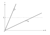
- FIG. 1 shows the relationship between the frequency and wave number of electromagnetic waves and plasma waves.
- the wave number k on the horizontal axis is proportional to 1 / ⁇ and is a quantity related to momentum.
- the frequency f on the vertical axis is an amount related to energy.
- the slope c of the straight line of the electromagnetic wave is the speed of light and is about 3 ⁇ 10 8 m / s.
- the slope v p of the straight line of the plasma wave is a value proportional to the root of the electron density n and is about 10 5 to 10 6 m / s.
- FIG. 1 is schematically illustrated, the slopes of the two curves differ by about two digits.
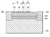
- FIG. 2 shows a conventional terahertz electromagnetic wave detection device that solves the above problem and enables mode conversion.
- the HEMT structure includes a substrate 201, an electron transit layer 202, an electron supply layer 203, a source 204, and a drain 205, and includes a first set of gates G1 and a second set of gates G2.
- the gate length L1 of each gate of the first set of gates G1 (each comb-like gate is called a “finger”) is greater than the gate length L2 of each gate of the second set of gates G2.
- Each gate of each set is arranged between the source 204 and the drain 205 with the same spatial period W.
- the first set of gates G1 and the second set of gates G2 are gratings having a period W and are interdigitated, so that the two sets of gates are combined. This is referred to as an “interdigitated dual-grating gate”.
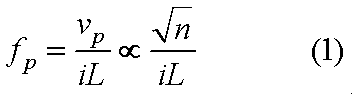
- i is an integer value of 2 or 4, and when both ends of the high electron concentration region under each gate are symmetrical boundaries, both ends become nodes or both ends become antinodes, and in the case of an asymmetric boundary, When one end is a node (antinode), the other end becomes an antinode (node).
- the first set of gates G1 has a higher electron density n and a smaller gate length L than the second set of gates G2, so that the resonance frequency is sufficiently higher for the first set of gates G1. Become a relationship.
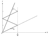
- Such periodicity of the resonance frequency of the plasma wave changes the straight line of the plasma wave shown in FIG.
- the straight line of the plasma wave is folded at a wave number ⁇ / W that is the boundary of the Brillouin zone due to the periodicity of the gate.
- the alternately arranged first and second gates G1 and G2 having the same period W function as antennas and enable mode conversion between terahertz electromagnetic waves and plasma waves.
- FIG. 3 is shown schematically, and considering the actual smallness of the slope v p , it should be noted that many frequencies satisfy both the energy conservation law and the momentum conservation law.
- the case where voltages are respectively applied to the first set of gates G1 and the second set of gates G2 has been described as an example. However, if one is set to a higher potential than the other, the same applies. The argument is established. For example, the second set of gates G2 may be short-circuited without applying a voltage, and the voltage may be applied only to the first set of gates G1.
- the resonance frequency will be different if the gate length is different, resulting in periodicity. To do.
- Patent Document 1 discloses a terahertz electromagnetic wave radiation element using the structure shown in FIG.
- the energy of the terahertz electromagnetic wave is converted into a plasma wave by the periodic antenna structure, in other words, the plasma wave can be excited.
- the plasma wave can be excited by some external factor, the energy of the plasma wave can be converted into a terahertz electromagnetic wave.
- Conversion from terahertz electromagnetic waves to plasma waves is an effective means as a detection mechanism for terahertz electromagnetic waves, while conversion from plasma waves to terahertz electromagnetic waves is an effective means as a generation mechanism for terahertz electromagnetic waves. Two mechanisms for detecting and generating these terahertz electromagnetic waves will be described below.
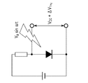
- a terahertz electromagnetic wave detection device means a device that outputs a DC voltage or current according to the incident power of a terahertz electromagnetic wave, using a Schottky barrier diode as a representative example.
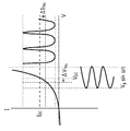
- the current / voltage characteristics of the diode have nonlinear characteristics in which the current increases exponentially with the voltage in the forward direction. As shown in FIG.
- the detection mechanism similar to that described above can be realized by the non-linearity of the plasma waves.
- the detection signal can be taken out as the fluctuation amount of the direct current or the direct voltage is the electrode portion of the transistor, the source electrode is grounded, the drain In the grounded source configuration in which the electrode is connected to the power supply through a load resistor, the electrode is extracted from the drain electrode as the amount of variation in the drain voltage.
- asymmetric boundary conditions both ends (source end and drain end) of the region in the electron transit layer where the plasma wave generates a standing wave have electrically different boundary conditions (hereinafter referred to as “asymmetric boundary conditions”). is there. From a different viewpoint, it can be seen that the energy of the terahertz electromagnetic wave is converted into direct current energy through a plasma wave placed under an asymmetric boundary condition.
- the electron transit layer of the transistor it accompanies thermal disturbance, DC current flowing from the drain to the source (microscopic electron DC drift running), and photoelectron / hole pairs generated by light absorption. Due to the presence of photocurrent and the like, the spatial distribution of electrons is always dense and varies with time. This density of electrons that varies with time is a plasma wave.
- a direct current flows between the source and drain due to a direct current drift of electrons, and both ends of the source and drain are in an asymmetric boundary condition of short circuit and open circuit, respectively, the amplitude of the plasma wave is multiplexed at the drain end. As reflection is repeated, it gradually increases and self-oscillation occurs. This is called plasma instability. The principle of this plasma instability will be further described.
- a plasma wave is a charge density wave due to local charge fluctuations moving at a certain speed caused by local fluctuations from a uniform electron concentration distribution. Accordingly, the current component of the plasma wave is given by the product of the local fluctuation amount e ⁇ n of the charge density and the plasma wave propagation velocity vp.
- e is an elementary charge
- ⁇ n is a local fluctuation amount of the electron density.
- the two operating mechanisms for detection and generation of terahertz electromagnetic waves can be summarized as follows. If the energy of terahertz electromagnetic waves can be efficiently converted into direct current energy through conversion between terahertz electromagnetic waves and plasma waves, a highly sensitive terahertz electromagnetic wave detection device will be developed. If direct current energy can be efficiently converted into terahertz electromagnetic waves, a highly efficient and high output terahertz electromagnetic wave generator can be configured.
- the conventional structure shown in FIG. 2 has a problem that conversion efficiency between terahertz electromagnetic wave energy and direct current energy via plasma waves is low.
- the present invention has been made in view of such problems, and an object of the present invention is to provide a terahertz electromagnetic wave energy and direct current via plasma waves in a field effect transistor structure terahertz electromagnetic wave converter having a source, a gate, and a drain.
- the purpose is to improve the conversion efficiency between energy.
- the “conversion device” is intended to include both a detection device that converts terahertz electromagnetic wave energy into DC energy via a plasma wave and a radiation device that converts DC energy into terahertz electromagnetic wave via a plasma wave. ing.
- a field effect transistor structure terahertz electromagnetic wave conversion device having a source, a gate, and a drain, wherein a plurality of fingers arranged in parallel at intervals are provided.
- a first set of gates and a second set of gates having a plurality of spaced apart parallel fingers on the surface of the field effect transistor structure;
- a first distance D1 and a second distance D2 between each finger and two fingers of the second set of gates adjacent to each finger are made unequal in length.
- the second aspect of the present invention is characterized in that, in the first aspect, D1 / D2 is about 0.55.
- the third aspect of the present invention is characterized in that, in the first or second aspect, the gate length of at least one pair of gates gradually decreases from the source toward the drain.
- a fourth aspect of the present invention is characterized in that, in the first or second aspect, the source is short-circuited and a DC bias current is applied between the source and the drain.
- the gate length of the first set of gates is narrower than the gate length of the second set of gates.
- the potential is higher than the potential of the second set of gates, and the electron density under the first set of gates is higher than the electron density under the second set of gates.
- the gate length of the first set of gates is narrower than the gate length of the second set of gates.
- the potential is equal to the potential of the second set of gates, and the electron density under the first set of gates is higher than the electron density under the second set of gates.
- the gate length of the first set of gates is equal to the gate length of the second set of gates.
- the potential is larger than the potential of the second set of gates, and the electron density under the first set of gates is higher than the electron density under the second set of gates.
- the gate lengths of the first set of gates gradually decrease from the source toward the drain. To do.
- the gate length is determined so that the ratio of the square root of the electron concentration to the gate length is a constant value in each finger of the first set of gates. It is characterized by being.
- a tenth aspect of the present invention is characterized in that, in any of the first to ninth aspects, the field effect transistor structure is a HEMT structure.
- a plurality of fingers arranged in parallel at intervals are provided.
- a first set of gates having the first set of gates and a second set of gates having a plurality of spaced apart parallel fingers on the surface of the field effect transistor structure;
- the plurality of fingers included in the gate and the plurality of fingers included in the second set of gates are alternately arranged, and are adjacent to each finger of the first set of gates and to the drain side of each of the fingers.
- the first distance D1 between the fingers of the second set of gates, the fingers, and the fingers adjacent to the source side of the fingers Characterized in that the fingers with the pair of gate unequal length and a second distance D2 between.
- each finger of the first set of gates G1 and the fingers of the second set of gates G2 arranged between the source 204 and the drain 205 each finger of the first set of gates G1 and the fingers
- the first distance D1 and the second distance D2 between the two fingers of the second set of gates G2 adjacent to each other are made unequal in length.
- the conversion efficiency between terahertz electromagnetic wave energy and direct current energy through waves can be improved by orders of magnitude.
- FIG. 1 is a diagram schematically showing the relationship between the frequency and wave number of electromagnetic waves and plasma waves.
- FIG. 2 is a diagram illustrating a conventional terahertz electromagnetic wave conversion device.
- FIG. 3 is a diagram schematically showing the relationship between the frequency and wave number of electromagnetic waves and plasma waves in the terahertz electromagnetic wave conversion device of FIG.
- FIG. 4A is a diagram illustrating a terahertz electromagnetic wave detection device using a Schottky barrier diode.
- FIG. 4B is a diagram for explaining nonlinearity of current / voltage characteristics of a Schottky barrier diode.
- FIG. 5 is a diagram showing a terahertz electromagnetic wave converter according to the present invention.
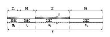
- FIG. 6 is a diagram showing a simulation model of the terahertz electromagnetic wave conversion device according to the present invention.
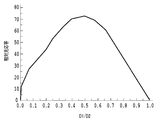
- FIG. 7 is a diagram illustrating a simulation result of the relationship between the relative light response and D1 / D2.
- FIG. 8 is a diagram showing a simulation result of the relationship between absorbance and D1 / D2.
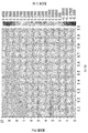
- FIG. 9 is a diagram illustrating a simulation result of the relationship between the optical response at each frequency and D1 / D2.
- FIG. 12 is a diagram illustrating a simulation result of the relationship between the relative light response and D1 / D2.
- FIG. 13 is a diagram showing a simulation result of the relationship between absorbance and D1 / D2.
- FIG. 14 is a diagram illustrating a simulation result of the relationship between the optical response at each frequency and D1 / D2.
- FIG. 5 shows a terahertz electromagnetic wave converter according to the present invention.
- the structure is almost the same as that of the conventional terahertz electromagnetic wave conversion device shown in FIG. 2, but each finger of the first set of gates G1 and two fingers of the second set of gates G2 adjacent to the fingers The first distance D1 and the second distance D2 between them are unequal lengths.
- the terahertz electromagnetic wave conversion device can be manufactured as follows. (1) First, a desired heteroepitaxial layer is grown on the semiconductor substrate 201. For example, a GaAs buffer layer (not shown) is epitaxially grown on a semi-insulating GaAs substrate 201, and an InGaAs layer is epitaxially grown thereon as the electron transit layer 202. Then, as an electron supply layer and a barrier layer on the electron transit layer 202, an InGaP layer is epitaxially grown (while locally doping Si as a donor), and a high layer for the source 204 and the drain 205 is formed thereon. A highly doped InGaAs layer (not shown) in which Si is implanted at a concentration is grown.
- the formation region of the source 204 and the drain 205 is specified by resist coating, light exposure and etching, and (5) the source 204 and the drain 205 are formed by metal deposition and lift-off.
- the first and second sets of gates G1 and G2 are formed by metal deposition and lift-off.
- a metal wiring portion (not shown) from the source 204, the drain 205, the first and second sets of gates G1 and G2 to the pad lead electrode portion (not shown) is formed by resist coating, light exposure and etching.
- the metal wiring portion is formed by metal vapor deposition and lift-off.
- passivation is performed with an insulating film (not shown) such as SiN.
- the pad lead electrode portion is specified by resist application, light exposure, and etching, and the insulating film on the pad lead electrode portion is removed.
- FIG. 6 shows a simulation model
- FIG. 7 shows a simulation result.
- the gate length L1 of the first set of gates G1 is 0.1 ⁇ m
- the gate length L2 of the second set of gates G2 is 0.6 ⁇ m
- the period W is 0.9 ⁇ m
- the number of repetitions of the basic periodic structure is 89 (accordingly,
- the distance of the electron transit layer 202 was 80.1 ⁇ m), and the distance d between the surface of the HEMT structure and the region where 2DEG was present was 65 nm.
- the source end was short-circuited, and the DC bias current between the source and the drain was 0.5 A (that is, 0.5 A / mm) per 1 mm of the gate width Lw (length in the depth direction perpendicular to the paper surface).
- Non-Patent Documents 1 to 3 For the specific method of simulation, refer to Non-Patent Documents 1 to 3. The outline of the method is as follows. (1) First, by applying the potentials of the first and second sets of gates G1 and G2 and the drain 205 and solving the Poisson equation, the charge density of the spatially distributed region of the two-dimensional electron layer Find the distribution. The charge density distribution is incorporated into the Maxwell equation and the spatial distribution of the electromagnetic field is solved. The plasma wave is given as a temporal and spatial variation of the charge density distribution. There are a time domain analysis and a frequency domain analysis as a solution method. Since the electric field distribution in the steady state may be obtained, the frequency domain analysis is adopted in this embodiment.
- the electric field, the magnetic field and the current component caused by them are defined as the fundamental standing wave defined by the periodic structure.
- the Galerkin method is employed in this embodiment (see Non-Patent Documents 1 and 2).
- Absorbance is given by the ratio of the real part of the spatial integral of the product of the current density and the electric field and the energy of the incident electromagnetic wave, that is, the ratio of the electromagnetic wave energy absorbed in the plasmon region to the incident electromagnetic wave energy according to Joule's law (Non-Patent Document). 2).
- the current component of the plasma wave is obtained as the product of the fluctuation of the charge density and the electron velocity by solving the hydrodynamic equation for the plasma wave in the two-dimensional electron layer. Can be calculated.
- the charge density and the electron velocity component can be analyzed by analyzing the Fourier series by expanding the Fourier series.
- Lw is the gate width (length in the depth direction)
- ⁇ 0 is the background DC conductivity (DC conductivity in a static state without local fluctuations in charge density and electron velocity) (see Non-Patent Document 3).
- the drain potential fluctuation amount ⁇ Vds per unit incident power 1 W of the terahertz electromagnetic wave is expressed as a photoresponse (unit: V / W).
- all terahertz electromagnetic waves are incident vertically from the upper part on the side where the gate electrode exists.
- the relative optical response has a peak at about 0.5, but if the relative optical response is 50 times or more is regarded as a significant improvement over the prior art, D1 / D2 is 0.23 ⁇ D1. It can be seen from FIG. 7 that /D2 ⁇ 0.72 is preferable.
- the ability to convert terahertz electromagnetic wave energy and direct current energy via plasma waves can be improved by orders of magnitude, that is, the light (terahertz electromagnetic wave) response sensitivity in the detection operation, and in the generation operation, It was found that the electromagnetic radiation intensity can be improved by orders of magnitude.
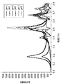
- FIG. 8 is a diagram showing a simulation result of the relationship between absorbance at each frequency and D1 / D2 using the model of FIG. FIG. 8 shows that the absorption of the terahertz electromagnetic wave is uniform without depending on D1 / D2, and that the absorbance is uniformly high at a specific frequency corresponding to the plasmon resonance frequency.
- FIG. 9 shows a simulation result of the relationship between the optical response at each frequency and D1 / D2.
- the optical response at 6.4 THz is normalized with this value, the relative optical response shown in FIG. The one corresponding to the graph is obtained.
- the gate length L1 of the first set of gates G1 is 0.5 ⁇ m
- the gate length L2 of the second set of gates G2 is 2.0 ⁇ m
- the period W is 4.0 ⁇ m
- the number of repetitions of the basic periodic structure is 50 (accordingly,
- the distance of the electron transit layer 202 was 200 ⁇ m)
- the distance d between the surface of the HEMT structure and the region where 2DEG was present was 40 nm.
- the source end was short-circuited
- the DC bias current between the source and the drain was 0.5 A (that is, 0.5 A / mm) per 1 mm of the gate width Lw (length in the depth direction perpendicular to the paper surface).
- This graph shows the electric field strength amplitude in the vicinity of the center of the gap on the left side of the second set of gates G2.
- FIG. 12 is a diagram illustrating a simulation result of the relationship between the relative light response and D1 / D2.
- the electron concentration N 1 in each region under the narrower gate is set to 2.57 ⁇ 10 16 m ⁇ 2, and the electron concentrations N 2 to N 4 in other regions are set to the same value 2.57 ⁇ 10. 15 m -2 is set.
- the other conditions are the same as those in FIGS.
- the gate length L1 of the first set of gates G1 is 0.1 ⁇ m
- the gate length L2 of the second set of gates G2 is 0.6 ⁇ m
- the period W is 0.9 ⁇ m
- the number of repetitions of the basic periodic structure is 89 ( Therefore, the distance of the electron transit layer 202 is 80.1 ⁇ m), and the distance d between the surface of the HEMT structure and the region where 2DEG exists is 65 nm.
- the source end was short-circuited, and the DC bias current between the source and the drain was set to 0.5 A (that is, 0.5 A / mm) per 1 mm of the gate width Lw.
- the relative optical response is about 5.5 ⁇ 10 3 , which is significantly improved by almost two digits compared to the result of FIG.
- This result is based on the actual operating conditions in which this device is actually used, and the plasma concentration in each region under the narrower gate with an electron concentration that is one digit higher due to the large difference in the electron concentration. This is due to the fact that the resonance phenomenon of the plasma wave shown in the equation (1) occurs more strongly because the wave is confined more strongly. Further, as compared with the result of FIG. 7, the dependence of relative light intensity on D1 / D2 is sensitive, and there are a plurality of peaks having different intensities.
- the optical response is caused by the superposition of the distortion component due to the nonlinear characteristic of the plasma wave, that is, the higher-order harmonic component with respect to the fundamental standing wave of the plasma wave.
- the spatial distribution of the electron concentration in the source / drain direction in the electron transit layer causes the phase characteristic of the higher-order harmonic component to be asymmetry of the electric field strength distribution determined by D1 / D2. It depends on sensitivity.
- strong D1 / D2 dependence appears in the optical response, which is the direct current component (the variation from the initial value of the time average value of the drain current component due to the plasma wave).
- FIG. 12 shows that the optical response sensitivity, that is, the detection sensitivity of the terahertz electromagnetic wave is greatly improved as in FIG. 7, but as described above, the plasma instability is clearly induced by realizing the asymmetric boundary condition. In addition, since the resonance phenomenon of the plasma wave is generated more strongly, the generation and radiation ability of the terahertz electromagnetic wave is remarkably improved.
- FIG. 13 is a diagram showing simulation results of the relationship between absorbance at each frequency and D1 / D2. 13 is a simulation using the model of FIG. 6 under the same conditions as FIG. From FIG. 13, as in FIG. 8, the absorbance of the terahertz electromagnetic wave is uniform without depending on D1 / D2, and the absorbance is uniformly high at a specific frequency (7.0 THz) corresponding to the plasmon resonance frequency. I understand that.
- FIG. 14 shows a simulation result of the relationship between the optical response at each frequency and D1 / D2.
- a technique disclosed in Patent Document 2 can be cited as a technique for suppressing the spectrum spread.
- the resonance frequency in each plasmon region is proportional to the ratio of the square root of the electron concentration n to the gate length L. Therefore, if the gate length is determined from the source to the drain so that this ratio becomes a constant value, it is possible to avoid the mismatch of the resonance frequencies and suppress the spectrum spread.
- the design is complicated, it is possible to make the period W constant and D1 / D2 constant.
- the finger periods of the first set of gates G1 and the second set of gates G2 are not constant, the asymmetric boundary condition can be realized by making D1 / D2 constant, and the present invention is effective. Note that it works.
- the ratio of the square root of the electron concentration n to the gate length L is a constant value, but by decreasing the gate length of at least one set of gates sequentially from the source to the drain, The effect of suppressing the spectrum spread can be obtained.
- the Brillouin zone described in FIG. 3 differs depending on the period, so that the return of the plasma wave dispersion characteristic at the Brillouin zone boundary is not uniform, and the terahertz electromagnetic wave and the plasma wave energy
- the position of the intersection between the dispersion line of the terahertz electromagnetic wave and the dispersion line of the plasma wave that can be converted is shifted for each finger of the gate.
- the speed of the terahertz electromagnetic wave and the speed of the plasma wave are more than two orders of magnitude, the intersection of the dispersion line of the terahertz electromagnetic wave and the dispersion line of the plasma wave that enables the energy conversion of the terahertz electromagnetic wave and the plasma wave.
- the fluctuation range of the finger period (the fluctuation range of the Brillouin zone boundary point) is at most within an order of magnitude. Even if it occurs, there is no obstacle to the conversion efficiency between the terahertz electromagnetic wave and the plasma wave.
Landscapes
- Junction Field-Effect Transistors (AREA)
- Electrodes Of Semiconductors (AREA)
Abstract
Description
(第1の実施形態)
(第2の実施形態)
Claims (11)
- ソース、ゲート及びドレインを有する電界効果トランジスタ構造のテラヘルツ電磁波変換装置において、
間隔をおいて並列に配置された複数のフィンガーを有する第1の組のゲートと、
間隔をおいて並列に配置された複数のフィンガーを有する第2の組のゲートと
を前記電界効果トランジスタ構造の表面上に備え、
前記第1の組のゲートの各フィンガーと、前記各フィンガーに隣接する前記第2の組のゲートの2つのフィンガーとの間の第1の距離D1と第2の距離D2を不等長とすることを特徴とするテラヘルツ電磁波変換装置。 - D1/D2が約0.55であることを特徴とする請求項1に記載のテラヘルツ電磁波変換装置。
- 前記ソースから前記ドレインに向かって、少なくとも一方の組のゲートのゲート長が順次狭くなることを特徴とする請求項1又は2に記載のテラヘルツ電磁波変換装置。
- 前記ソースが短絡され、前記ソースと前記ドレインとの間に直流バイアス電流が印加されていることを特徴とする請求項1又は2に記載のテラヘルツ電磁波変換装置。
- 前記第1の組のゲートのゲート長は、前記第2の組のゲートのゲート長より狭く、
前記第1の組のゲートの電位は、前記第2の組のゲートの電位よりも高く、
前記第1の組のゲートの下の電子密度は、前記第2の組のゲートの下の電子密度よりも高いことを特徴とする請求項4に記載のテラヘルツ電磁波変換装置。 - 前記第1の組のゲートのゲート長は、前記第2の組のゲートのゲート長より狭く、
前記第1の組のゲートの電位は、前記第2の組のゲートの電位と等しく、
前記第1の組のゲートの下の電子密度は、前記第2の組のゲートの下の電子密度よりも高いことを特徴とする請求項4に記載のテラヘルツ電磁波変換装置。 - 前記第1の組のゲートのゲート長は、前記第2の組のゲートのゲート長と等しく、
前記第1の組のゲートの電位は、前記第2の組のゲートの電位よりも大きく、
前記第1の組のゲートの下の電子密度は、前記第2の組のゲートの下の電子密度よりも高いことを特徴とする請求項4に記載のテラヘルツ電磁波変換装置。 - 前記ソースから前記ドレインに向かって、前記第1の組のゲートのゲート長が順次狭くなることを特徴とする請求項5から7のいずれかに記載のテラヘルツ電磁波変換装置。
- 前記第1の組のゲートの各フィンガーにおいて、ゲート長に対する電子濃度の平方根の比が一定値となるようにゲート長が定まっていることを特徴とする請求項8に記載のテラヘルツ電磁波変換装置。
- 前記電界効果トランジスタ構造は、HEMT構造であることを特徴とする請求項1から9のいずれかに記載のテラヘルツ電磁波変換装置。
- ソース、第1及び第2の組のゲート並びにドレインを有する電界効果トランジスタ構造のテラヘルツ電磁波変換装置において、
間隔をおいて並列に配置された複数のフィンガーを有する前記第1の組のゲートと、
間隔をおいて並列に配置された複数のフィンガーを有する前記第2の組のゲートと
を前記電界効果トランジスタ構造の表面上に備え、
前記第1の組のゲートが有する複数のフィンガーと、前記第2の組のゲートが有する複数のフィンガーは、交互に配置されており、
前記第1の組のゲートの各フィンガーと、前記各フィンガーのドレイン側に隣接する、前記第2の組のゲートが有するフィンガーとの間の第1の距離D1と、前記各フィンガーと、前記各フィンガーのソース側に隣接する、前記第2の組のゲートが有するフィンガーとの間の第2の距離D2とを不等長とすることを特徴とするテラヘルツ電磁波変換装置。
Priority Applications (4)
| Application Number | Priority Date | Filing Date | Title |
|---|---|---|---|
| PCT/JP2010/007074 WO2012073298A1 (ja) | 2010-12-03 | 2010-12-03 | テラヘルツ電磁波変換装置 |
| EP10860400.0A EP2648290A4 (en) | 2010-12-03 | 2010-12-03 | ELECTROMAGNETIC TERAHTIC WAVE CONVERTER |
| US13/991,407 US9018683B2 (en) | 2010-12-03 | 2010-12-03 | Terahertz electromagnetic wave conversion device |
| JP2012546581A JP5747420B2 (ja) | 2010-12-03 | 2010-12-03 | テラヘルツ電磁波変換装置 |
Applications Claiming Priority (1)
| Application Number | Priority Date | Filing Date | Title |
|---|---|---|---|
| PCT/JP2010/007074 WO2012073298A1 (ja) | 2010-12-03 | 2010-12-03 | テラヘルツ電磁波変換装置 |
Publications (1)
| Publication Number | Publication Date |
|---|---|
| WO2012073298A1 true WO2012073298A1 (ja) | 2012-06-07 |
Family
ID=46171286
Family Applications (1)
| Application Number | Title | Priority Date | Filing Date |
|---|---|---|---|
| PCT/JP2010/007074 Ceased WO2012073298A1 (ja) | 2010-12-03 | 2010-12-03 | テラヘルツ電磁波変換装置 |
Country Status (4)
| Country | Link |
|---|---|
| US (1) | US9018683B2 (ja) |
| EP (1) | EP2648290A4 (ja) |
| JP (1) | JP5747420B2 (ja) |
| WO (1) | WO2012073298A1 (ja) |
Cited By (4)
| Publication number | Priority date | Publication date | Assignee | Title |
|---|---|---|---|---|
| JP2015175957A (ja) * | 2014-03-14 | 2015-10-05 | 日本電信電話株式会社 | 周波数可変フィルタ |
| JP2017510067A (ja) * | 2014-02-24 | 2017-04-06 | ユニスト(ウルサン ナショナル インスティテュート オブ サイエンス アンド テクノロジー)Unist (Ulsan National Institute Of Science And Technology) | プラズマ波トランジスタの性能を評価する方法 |
| JP2017525170A (ja) * | 2014-12-30 | 2017-08-31 | ユニスト(ウルサン ナショナル インスティテュート オブ サイエンス アンド テクノロジー)Unist (Ulsan National Institute Of Science And Technology) | 電磁波発振器、プラズマ波電力抽出器及び電磁波検出器 |
| JP2018517887A (ja) * | 2015-12-31 | 2018-07-05 | ユニスト(ウルサン ナショナル インスティテュート オブ サイエンス アンド テクノロジー) | サスペンデッドチャネルプラズマ波トランジスタの性能評価方法 |
Families Citing this family (9)
| Publication number | Priority date | Publication date | Assignee | Title |
|---|---|---|---|---|
| US9297638B1 (en) * | 2014-10-21 | 2016-03-29 | Sandia Corporation | Two-path plasmonic interferometer with integrated detector |
| JP6299665B2 (ja) * | 2015-04-30 | 2018-03-28 | 三菱電機株式会社 | 電界効果トランジスタ |
| CN105336809B (zh) * | 2015-11-09 | 2017-10-20 | 中国工程物理研究院电子工程研究所 | 具有阵列导电沟道结构的太赫兹波探测器 |
| KR101777929B1 (ko) | 2015-12-31 | 2017-09-13 | 울산과학기술원 | 서스펜디드 채널 플라즈마파 트랜지스터의 성능 평가 방법 |
| WO2018063291A1 (en) * | 2016-09-30 | 2018-04-05 | Intel Corporation | Single-flipped resonator devices with 2deg bottom electrode |
| US11218144B2 (en) | 2019-09-12 | 2022-01-04 | Vishay-Siliconix, LLC | Semiconductor device with multiple independent gates |
| TWI803845B (zh) * | 2021-03-24 | 2023-06-01 | 新唐科技股份有限公司 | 半導體結構 |
| CN113257910B (zh) * | 2021-05-11 | 2023-01-03 | 华南师范大学 | 梳型栅结构hemt射频器件及其制备方法 |
| EP4723176A1 (en) | 2023-05-31 | 2026-04-08 | Tohoku University | Frequency down-conversion device and communication device |
Citations (2)
| Publication number | Priority date | Publication date | Assignee | Title |
|---|---|---|---|---|
| WO2006030608A1 (ja) | 2004-09-13 | 2006-03-23 | Kyushu Institute Of Technology | テラヘルツ電磁波放射素子及びその製造方法 |
| JP2009224467A (ja) | 2008-03-14 | 2009-10-01 | Tohoku Univ | 電磁波放射素子 |
-
2010
- 2010-12-03 US US13/991,407 patent/US9018683B2/en not_active Expired - Fee Related
- 2010-12-03 WO PCT/JP2010/007074 patent/WO2012073298A1/ja not_active Ceased
- 2010-12-03 JP JP2012546581A patent/JP5747420B2/ja not_active Expired - Fee Related
- 2010-12-03 EP EP10860400.0A patent/EP2648290A4/en not_active Withdrawn
Patent Citations (2)
| Publication number | Priority date | Publication date | Assignee | Title |
|---|---|---|---|---|
| WO2006030608A1 (ja) | 2004-09-13 | 2006-03-23 | Kyushu Institute Of Technology | テラヘルツ電磁波放射素子及びその製造方法 |
| JP2009224467A (ja) | 2008-03-14 | 2009-10-01 | Tohoku Univ | 電磁波放射素子 |
Non-Patent Citations (10)
| Title |
|---|
| D. COQUILLAT ET AL.: "Room temperature detection of sub-terahertz radiation in double-grating-gate transistors", OPTICS EXPRESS, vol. 18, no. 6, 15 March 2010 (2010-03-15), pages 6024 - 6032, XP002723604 * |
| D. COQUILLAT ET AL.: "Terahertz detection in a double-grating-gate heterotransistor", JOURNAL OF PHYSICS: CONFERENCE SERIES, vol. 193, 2009, pages 012074, XP020170433 * |
| D. V. FATEEV; V. V. POPOV; M. S. SHUR: "Transformation of the Plasmon Spectrum in a Grating Gate Transistor Structure with Spatially Modulated Two Dimensional Electron Channel", SEMICONDUCTORS, vol. 44, no. 11, 2010, pages 1406 - 1413, XP019863600, DOI: doi:10.1134/S1063782610110059 |
| G. R. AIZIN; D. V. GATEEV; G. M. TSYMBALOV; V. V. POPOV: "Terahertz plasmon photoresponse in a density modulated two-dimensional electron channel of a GaAs/AlGaAs field-effect transistor", APPL. PHYS. LETT., vol. 91, no. 163507, 2007, pages 3 |
| IRINA KHMYROVA ET AL.: "Analysis of terahertz plasma resonances in structures with two-dimensional electron systems periodically modulated by interdigitated gate", JOURNAL OF APPLIED PHYSICS, vol. 108, 8 October 2010 (2010-10-08), pages 074511, XP012143187 * |
| M. DYAKONOV; M. SHUR, IEEE TRANS. ELECTRON DEVICES, vol. 43, 1996, pages 380 - 387 |
| M. DYAKONOV; M. SHUR, PHYS. REV. LETT. VOL., vol. 71, 1993, pages 2465 - 2468 |
| See also references of EP2648290A4 |
| TAKUYA NISHIMURA ET AL.: "An Intensity Modulator for Terahertz Electromagnetic Waves Utilizing Two-Dimensional Plasmon Resonance in a Dual-Grating-Gate High-Electron-Mobility Transistor", JAPANESE JOURNAL OF APPLIED PHYSICS, vol. 49, 20 March 2010 (2010-03-20), pages 054301, XP055119075 * |
| V. V. POPOV; G. M. TSYMBALOVANDM; S. SHUR: "Plasma wave in-stability and amplification of terahertz radiation in field-effect-transistor arrays", J. PHYS.: CONDENS. MATTER, vol. 20, no. 384208, 2008, pages 6 |
Cited By (6)
| Publication number | Priority date | Publication date | Assignee | Title |
|---|---|---|---|---|
| JP2017510067A (ja) * | 2014-02-24 | 2017-04-06 | ユニスト(ウルサン ナショナル インスティテュート オブ サイエンス アンド テクノロジー)Unist (Ulsan National Institute Of Science And Technology) | プラズマ波トランジスタの性能を評価する方法 |
| JP2015175957A (ja) * | 2014-03-14 | 2015-10-05 | 日本電信電話株式会社 | 周波数可変フィルタ |
| JP2017525170A (ja) * | 2014-12-30 | 2017-08-31 | ユニスト(ウルサン ナショナル インスティテュート オブ サイエンス アンド テクノロジー)Unist (Ulsan National Institute Of Science And Technology) | 電磁波発振器、プラズマ波電力抽出器及び電磁波検出器 |
| US10161804B2 (en) | 2014-12-30 | 2018-12-25 | Unist (Ulsan National Institute Of Science And Technology) | Electromagnetic wave oscillator, plasma wave power extractor and electromagnetic wave detector |
| JP2018517887A (ja) * | 2015-12-31 | 2018-07-05 | ユニスト(ウルサン ナショナル インスティテュート オブ サイエンス アンド テクノロジー) | サスペンデッドチャネルプラズマ波トランジスタの性能評価方法 |
| US10684320B2 (en) | 2015-12-31 | 2020-06-16 | Unist (Ulsan National Institute Of Science And Technology) | Performance evaluation method of suspended channel plasma wave transistor |
Also Published As
| Publication number | Publication date |
|---|---|
| EP2648290A4 (en) | 2014-06-18 |
| JP5747420B2 (ja) | 2015-07-15 |
| US20130277716A1 (en) | 2013-10-24 |
| EP2648290A1 (en) | 2013-10-09 |
| US9018683B2 (en) | 2015-04-28 |
| JPWO2012073298A1 (ja) | 2014-05-19 |
Similar Documents
| Publication | Publication Date | Title |
|---|---|---|
| JP5747420B2 (ja) | テラヘルツ電磁波変換装置 | |
| Popov | Plasmon excitation and plasmonic detection of terahertz radiation in the grating-gate field-effect-transistor structures | |
| JP4423429B2 (ja) | テラヘルツ電磁波放射素子及びその製造方法 | |
| JP6169614B2 (ja) | プラズモン電極を有する光伝導装置 | |
| US6635898B2 (en) | Quantum computer | |
| Otsuji et al. | Emission and detection of terahertz radiation using two-dimensional plasmons in semiconductor nanoheterostructures for nondestructive evaluations | |
| Degl’Innocenti et al. | Fast modulation of terahertz quantum cascade lasers using graphene loaded plasmonic antennas | |
| Gao et al. | Graphene-on-silicon nitride waveguide photodetector with interdigital contacts | |
| Yan et al. | A low-noise on-chip coherent microwave source | |
| Cosme et al. | Terahertz laser combs in graphene field-effect transistors | |
| CN102257406A (zh) | 探测电磁辐射的设备和方法 | |
| Chen et al. | Enhanced electron-phonon coupling for a semiconductor charge qubit in a surface phonon cavity | |
| Aizin et al. | Plasma instability and amplified mode switching effect in THz field effect transistors with a grating gate | |
| Zeng et al. | Ultrafast hot carrier cooling enabled van der Waals photodetectors at telecom wavelengths | |
| Tkachenko et al. | Photon-stimulated transport in a quantum point contact (brief review) | |
| US9153680B2 (en) | Stimulated phonon emission device and oscillator, frequency filter, cooling device, light-receiving device, and light-emitting device comprising the stimulated phonon emission device | |
| Mao et al. | Bandwidth limitation of directly contacted graphene–silicon optoelectronics | |
| Gholami et al. | Enhancement of the intensity and bandwidth of terahertz radiation in photoconductive dipole antennas | |
| Moradiannejad | Improvement of terahertz photoconductive antennas array using crossfingers structure | |
| Daneshmandian et al. | Numerical modeling of highly sensitive resonant detection of THz radiation using a multichannel dispersive plasmonic HEMT | |
| 阎蒋伟 et al. | Room-temperature THz detection via EIW effect based on graphite nanosheet | |
| Xia et al. | Experimental realization of a metasurface-based PETS THz detector | |
| Poyser et al. | A high electron mobility phonotransistor | |
| Briones et al. | Efficiency of broadband terahertz rectennas based on self-switching nanodiodes | |
| Zhang et al. | Resonant THz detection by periodic multi-gate plasmonic FETs |
Legal Events
| Date | Code | Title | Description |
|---|---|---|---|
| 121 | Ep: the epo has been informed by wipo that ep was designated in this application |
Ref document number: 10860400 Country of ref document: EP Kind code of ref document: A1 |
|
| ENP | Entry into the national phase |
Ref document number: 2012546581 Country of ref document: JP Kind code of ref document: A |
|
| NENP | Non-entry into the national phase |
Ref country code: DE |
|
| WWE | Wipo information: entry into national phase |
Ref document number: 13991407 Country of ref document: US |
|
| WWE | Wipo information: entry into national phase |
Ref document number: 2010860400 Country of ref document: EP |