WO2012095902A1 - 光源装置 - Google Patents
光源装置 Download PDFInfo
- Publication number
- WO2012095902A1 WO2012095902A1 PCT/JP2011/004345 JP2011004345W WO2012095902A1 WO 2012095902 A1 WO2012095902 A1 WO 2012095902A1 JP 2011004345 W JP2011004345 W JP 2011004345W WO 2012095902 A1 WO2012095902 A1 WO 2012095902A1
- Authority
- WO
- WIPO (PCT)
- Prior art keywords
- case
- light source
- source device
- mounting substrate
- circuit unit
- Prior art date
- Legal status (The legal status is an assumption and is not a legal conclusion. Google has not performed a legal analysis and makes no representation as to the accuracy of the status listed.)
- Ceased
Links
Images


Classifications
-
- F—MECHANICAL ENGINEERING; LIGHTING; HEATING; WEAPONS; BLASTING
- F21—LIGHTING
- F21K—NON-ELECTRIC LIGHT SOURCES USING LUMINESCENCE; LIGHT SOURCES USING ELECTROCHEMILUMINESCENCE; LIGHT SOURCES USING CHARGES OF COMBUSTIBLE MATERIAL; LIGHT SOURCES USING SEMICONDUCTOR DEVICES AS LIGHT-GENERATING ELEMENTS; LIGHT SOURCES NOT OTHERWISE PROVIDED FOR
- F21K9/00—Light sources using semiconductor devices as light-generating elements, e.g. using light-emitting diodes [LED] or lasers
- F21K9/20—Light sources comprising attachment means
- F21K9/23—Retrofit light sources for lighting devices with a single fitting for each light source, e.g. for substitution of incandescent lamps with bayonet or threaded fittings
-
- F—MECHANICAL ENGINEERING; LIGHTING; HEATING; WEAPONS; BLASTING
- F21—LIGHTING
- F21V—FUNCTIONAL FEATURES OR DETAILS OF LIGHTING DEVICES OR SYSTEMS THEREOF; STRUCTURAL COMBINATIONS OF LIGHTING DEVICES WITH OTHER ARTICLES, NOT OTHERWISE PROVIDED FOR
- F21V23/00—Arrangement of electric circuit elements in or on lighting devices
- F21V23/003—Arrangement of electric circuit elements in or on lighting devices the elements being electronics drivers or controllers for operating the light source, e.g. for a LED array
- F21V23/004—Arrangement of electric circuit elements in or on lighting devices the elements being electronics drivers or controllers for operating the light source, e.g. for a LED array arranged on a substrate, e.g. a printed circuit board
- F21V23/006—Arrangement of electric circuit elements in or on lighting devices the elements being electronics drivers or controllers for operating the light source, e.g. for a LED array arranged on a substrate, e.g. a printed circuit board the substrate being distinct from the light source holder
-
- F—MECHANICAL ENGINEERING; LIGHTING; HEATING; WEAPONS; BLASTING
- F21—LIGHTING
- F21Y—INDEXING SCHEME ASSOCIATED WITH SUBCLASSES F21K, F21L, F21S and F21V, RELATING TO THE FORM OR THE KIND OF THE LIGHT SOURCES OR OF THE COLOUR OF THE LIGHT EMITTED
- F21Y2115/00—Light-generating elements of semiconductor light sources
- F21Y2115/10—Light-emitting diodes [LED]
Definitions
- the present invention relates to a light source device using a light emitting module such as an LED (light emitting diode) module as a light source.
- a light emitting module such as an LED (light emitting diode) module
- Such a light source device generally includes a circuit unit including a plurality of electronic components for lighting an LED module and a mounting board on which the electronic components are mounted, and the circuit unit is disposed inside an insulating case. .
- Patent Document 1 discloses that a circuit unit is vertically arranged inside a cylindrical case.
- the vertical arrangement means that the circuit unit is arranged so that the mounting board is parallel to the cylindrical axis of the case, and thereby the mounting board, which is one of the most bulky members, is efficiently accommodated inside the case. Is possible.
- the circuit unit when the circuit unit is arranged vertically in the cylindrical case, it is preferable to arrange the mounting board at a position close to the cylindrical axis of the case.
- region inside a case can be utilized effectively, and the accommodation of the mounting board
- the mounting board is arranged at a position close to the cylinder axis, the maximum gap width between the mounting surface of the mounting board and the inner peripheral surface of the case becomes approximately half of the inner diameter of the case. Therefore, it becomes difficult to mount a tall electronic component on the mounting board.
- an object of the present invention is to provide a light source device that can accommodate a circuit unit having a tall electronic component and a wide mounting substrate in a small case.
- a light source device includes a light emitting module as a light source, a plurality of electronic components for lighting the light emitting module, and a circuit unit having a mounting substrate on which they are mounted, and at least A cylindrical case having an opening at one end and accommodating the circuit unit therein, wherein the mounting substrate is inclined with respect to the cylindrical axis of the case, and It is held by the case in an arrangement that does not intersect the cylinder axis.
- the light source device according to the present invention is held by the case in an attitude that is inclined with respect to the cylinder axis of the case and that does not intersect the cylinder axis, the light source device is more than in the case where the mounting substrate is arranged vertically.
- the maximum gap width between the main surface of the mounting substrate on the cylinder shaft side and the inner peripheral surface of the case can be increased, and a taller electronic component can be mounted on the mounting substrate, and the vertical arrangement
- a mounting board having substantially the same width as that of the case can be accommodated in the case.
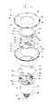
- the perspective view which shows the light source device which concerns on this embodiment Exploded sectional view showing the light source device according to the present embodiment
- the scale of the member in each drawing differs from an actual thing.
- the symbol “ ⁇ ” used to indicate a numerical range includes numerical values at both ends.
- the alternate long and short dash line indicates the lamp axis J, and the direction indicated by the arrow X parallel to the lamp axis J is the front of the light source device and also the illumination direction.
- FIG. 1 is a perspective view showing a light source device according to this embodiment.
- FIG. 2 is an exploded cross-sectional view showing the light source device according to the present embodiment.
- the light source device is an LED lamp 1 having a shape conforming to the halogen bulb standard defined in JIS C 7527, and can be a substitute for the halogen bulb.
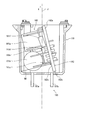
- the LED lamp 1 includes a body 10, a light emitting module 20, an optical member 30, a front cover 40, an insulating member 50, a circuit unit 60, a case 70, and a base 80.
- the body 10 has a bowl shape having an opening 11 on the front side, and has a substantially cylindrical tube portion 12 that gradually increases in diameter from the rear toward the front, and a substantially disk-shaped bottom portion that closes the rear of the tube portion 12. 13.
- the cylinder axis of the cylinder portion 12 (which is also the cylinder axis of the body 10) coincides with the lamp axis J.
- the shape of the body 10 is not limited to the above.
- a cylindrical shape having openings on both the front and rear sides may be used.
- an elliptical cylindrical shape or a rectangular cylindrical shape may be used.
- the diameter of the cylinder part 12 may be gradually reduced from the rear to the front, or may be uniform along the cylinder axis.
- the light emitting module 20 and the optical member 30 are accommodated in the body 10. Since the body 10 is made of metal, the body 10 functions as a heat sink that releases heat generated in the internal light emitting module 20 to the outside.
- the metal used for the body 10 is preferably aluminum in consideration of heat dissipation, heat resistance, light weight, and the like.
- a substantially annular flange portion 14 is provided at the opening side end portion 10 a of the cylindrical portion 12 so as to surround the opening 11.
- the front cover 40 is attached to the opening-side end portion 10 a by locking the claw portion 44 to the flange portion 14.
- a plurality of protrusions 15 are provided on the rear surface of the flange portion 14 with a gap in the circumferential direction of the flange portion.
- the protrusion 15 suppresses the idling of the front cover 40 with respect to the body 10. That is, when the front cover 40 is rotated around the lamp axis J, the claw portion 44 rotates and hits the protrusion 15, so that the front cover 40 does not idle with respect to the body 10.
- the number of the protrusions 15 is arbitrary.
- the light emitting module 20 is a light source of the LED lamp 1, and includes a module substrate 21 and an LED unit 22 mounted substantially at the center of the module substrate 21, and is mounted at a substantially central position on the bottom 13 inside the body 10. ing.
- the LED unit 22 is, for example, a substantially hemisphere including a unit substrate 23, an InGaN-based LED chip 24 with a blue emission color mounted on the unit substrate 23, and a yellow-green light emitting phosphor that seals the LED chip 24. A part of blue light emitted from the LED chip 24 is converted into yellow-green color by a phosphor, and white light generated by the color mixture of blue and yellow-green is emitted. .
- the optical member 30 is made of a translucent material such as a transparent acrylic resin, for example, and has a substantially truncated cone-shaped lens portion 31 and a substantially annular plate-shaped outer edge portion extending on the peripheral surface of the lens portion 31. 32, and the lens portion 31 and the outer edge portion 32 are integrally formed.
- the lens unit 31 is located approximately in the center of the body 10 and in front of the light emitting module 20.
- the lens portion 31 has a substantially cylindrical recess 33 at the rear end, and the optical member 30 is positioned with respect to the LED unit 22 by fitting the sealing portion 25 of the LED unit 22 into the recess 33. Yes.
- the emitted light from the light emitting module 20 is mainly incident into the lens unit 31 from the concave portion 33, passes through the lens unit 31, and is extracted from the front surface of the lens unit 31 to the outside of the body 10.
- the light distribution characteristic of the emitted light changes. Specifically, the emitted light is focused by the lens unit 31 and becomes spot light similar to a halogen bulb with a reflecting mirror.
- the front surface of the lens unit 31 is subjected to light diffusion processing provided with a plurality of projections and depressions for diffusing outgoing light, for example.
- the outer edge portion 32 is located on the rear side of the front cover 40 so as to close the opening 11 of the body 10, and the front surface of the outer edge portion 32 and the rear surface of the front cover 40 face each other in surface contact. Since the outer edge portion 32 and the front cover 40 are in surface contact, the heat of the optical member 30 is easily conducted to the front cover 40. Therefore, the heat generated in the LED unit 22 can be efficiently released from the front cover 40 to the outside via the optical member 30. Moreover, since the front of the outer edge portion 32 is covered with the front cover 40, the light emitting module 20 housed in the body 10 is difficult to see through from the outside, and the appearance characteristics of the LED lamp 1 are good. When the front cover 40 is translucent, the light slightly leaking from the optical member 30 can be transmitted, and there is an effect that the entire front surface of the lamp shines.
- the front cover 40 includes, for example, a flat plate-shaped main body portion 42 having a substantially circular light emission window 41 and a short cylindrical peripheral wall portion 43 extending rearward from the outer peripheral edge of the main body portion 42. .
- the shape of the front cover 40 is not limited to the above, and may be any shape according to the shape of the opening 11 of the body 10.
- the front cover 40 is made of a non-translucent resin such as white PBT (polybutylene terephthalate). PBT is suitable as a material for the front cover 40 because it has high heat resistance, moderate elasticity, and excellent weather resistance.
- the resin constituting the front cover 40 is not limited to PBT, and may be acrylic, PC (polycarbonate), or the like. Further, the color of the front cover 40 is not limited to white and is arbitrary. It may be transparent or translucent.
- the peripheral wall portion 43 is provided with a plurality of claw portions 44 while being spaced apart along the circumferential direction of the peripheral wall portion 43.
- the claw portions 44 are arranged in the vicinity of the rear side edge on the inner peripheral surface of the peripheral wall portion 43 while being equally spaced along the circumferential direction of the peripheral wall portion 43. Projecting toward the J side.
- the number of the claw portions 44 is arbitrary.
- the body portion 42 is provided with a hole 45 at a position corresponding to the claw portion 44. Since such a hole 45 is provided, the front cover 40 having a complicated shape can be resin-molded with a simple mold having a small number of components, and simplification at the time of molding can be achieved.
- the front cover 40 urges the optical member 30 rearward, whereby the front cover 40 and the outer edge portion 32 are in surface contact, and the lens portion 31 is in contact with the light emitting module 20.
- the movement of the optical member 30 in the front-rear direction is restricted, and the positional deviation or rattling of the optical member 30 is prevented.
- the front cover 40 and the outer edge portion 32 are more closely attached, heat is easily conducted from the optical member 30 to the front cover 40, and the heat dissipation of the LED lamp 1 is improved.
- the insulating member 50 is for electrically insulating the circuit unit 60 and the body 10, and is formed of an insulating material such as resin or ceramic.
- the insulating member 50 has a substantially disk shape that is substantially the same diameter as the bottom portion 13 of the body 10, and is disposed behind the bottom portion 13.
- the insulating member 50 is not necessarily a necessary member. In the case where the insulating member 50 is not provided, a part of the electronic components 61 a to 61 f in the case 70 may be in contact with the body 10. Thereby, the heat of the electronic components 61a to 61f can be released to the body 10 side.
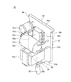
- FIG. 3 is a perspective view showing the circuit unit according to the present embodiment.
- the circuit unit 60 includes, for example, a rectifier circuit that rectifies AC power supplied from a commercial power source into DC power, and a voltage adjustment circuit that adjusts the voltage value of the DC power rectified by the rectifier circuit.
- the lighting circuit which consists of etc. is included.
- the circuit unit 60 is electrically connected to the base 80 and the LED unit 22, receives power from a lighting fixture (not shown) via the base 80, and causes the LED chip 24 of the LED unit 22 to emit light.
- the circuit unit 60 includes electronic components 61a to 61f for lighting the LED module 10, such as a choke coil 61a, an electrolytic capacitor 61b, a capacitor 61c, an IC 61d, a noise filter 61e, and a resistor 61f.
- Each circuit function of the circuit unit 60 is achieved by electronic components 61a to 61f, and these electronic components 61a to 61f are mounted on a plate-shaped mounting substrate 62.
- the mounting substrate 62 includes a main body 63 positioned on the front side in the case 70, a front end 64 positioned on the rear side, a connection 65 connecting the main body 63 and the front end 64, and a front of the main body 63. It is comprised with a pair of convex part 66 extended from the side edge part to the side.
- the front end 62a of the mounting substrate 62 (the end close to the opening 70a of the case 70) includes a front end of the main body 63 and a pair of convex portions 66.
- the rear end 62 b of the mounting substrate 62 (the end on the side far from the opening 70 a of the case 70) is constituted by the rear end of the tip 64.
- the main body 63 has a lateral width from the rear side toward the front side (a width in a direction parallel to the main surfaces 62c and 62d of the mounting substrate 62 and perpendicular to the lamp axis J. ”Means a width in the above direction.
- the choke coil 61a, the electrolytic capacitor 61b, the capacitor 61c, the IC 61d, and the noise filter 61e are mounted.
- the connecting portion 65 has a substantially trapezoidal shape in which the lateral width gradually decreases from the front side toward the rear side, and the resistor 61f is mounted thereon.
- the distal end portion 64 has a substantially rectangular shape with a narrower width than the main body portion 63.
- the convex portion 66 has a substantially square shape, and the distal end portion in the extending direction has an R shape.
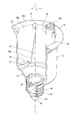
- FIG. 4 is a cross-sectional perspective view showing the case and the base according to the present embodiment.
- the case 70 has, for example, a cylindrical shape having an opening on the front side and the rear side, a large diameter portion 71, a small diameter portion 72 having an outer diameter and an inner diameter smaller than the large diameter portion 71, and a large size thereof. It has a reduced diameter portion 73 that connects the diameter portion 71 and the small diameter portion 72.
- the large diameter portion 71 is located on the front side and the small diameter portion 72 is located on the rear side, and the reduced diameter portion 73 is gradually reduced in diameter from the front side toward the rear side.
- the shape of the case 70 is not limited to the above.
- it may be a bottomed cylinder with no opening on the rear side.
- an elliptical cylindrical shape or a rectangular cylindrical shape may be used.
- the diameters of the large diameter portion 71, the small diameter portion 72, and the reduced diameter portion 73 may be changed in any manner or may be uniform.
- the case 70 has a function of ensuring the insulation of the circuit unit 60, and is formed of an insulating material such as resin or ceramic.
- the case 70 is attached to the rear side of the body 10 in a state where the opening 70 a on the front side is closed with the insulating member 50, and the circuit unit 60 and the body 10 are electrically insulated by the insulating member 50.
- a pair of first positioning portions 74 for positioning the front end 62a of the mounting substrate 62 is provided on the inner peripheral surface 71a of the large-diameter portion 71 (also the inner peripheral surface of the case 70).
- Each first positioning portion 74 is a recess formed in the end surface 70 b on the opening 70 a side of the case 70, and the recess is in communication with the internal space of the case 70.
- the front end 62a of the mounting substrate 62 is positioned by fitting the pair of convex portions 66 of the mounting substrate 62 into these recesses.
- the inner peripheral surface 71a of the large-diameter portion 71 is provided with a pair of protrusions 75 facing each other more specifically on the inner peripheral surface of the rear-side edge portion of the large-diameter portion 71.
- the pair of projecting portions 75 restricts the rear end 62 b of the mounting substrate 62 from approaching the lamp axis J.
- the inner peripheral surface 71a of the large diameter portion 71 more specifically, a pair of ribs opposed to each other on the inner peripheral surface of the portion from the rear side edge to the vicinity of the front side edge of the large diameter portion 71
- a portion 76 is provided along the lamp axis J.
- the pair of rib portions 76 restrict the rear end portion 62 b of the mounting substrate 62 from moving away from the lamp axis J.
- Adjacent protrusions 75 and ribs 76 constitute a second positioning portion 77 for positioning the rear end 62b of the mounting substrate 62.
- Each rib portion 76 has an inclined surface 76a for contacting the main surface 62d on the mounting substrate 62 opposite to the lamp axis J. These inclined surfaces 76a are included on the same virtual plane.
- Each bulging part 78 is provided from the front side edge of the large diameter part 71 to the rear side edge along the lamp axis J, and a screw hole 78a is formed in each front surface.
- a part of the surface of the bulging portion 78 may be an inclined surface.
- the base 80 is a member for receiving electric power from a socket (not shown) of the lighting fixture when the LED lamp 1 is attached to the lighting fixture and turned on.
- the type of the base 80 is not particularly limited, but an E11 base that is an Edison type is used in the present embodiment.
- the base 80 includes a shell portion 81 having a substantially cylindrical shape and an outer peripheral surface formed as a male screw, and an eyelet portion 83 attached to the shell portion 81 via an insulating portion 82, and a small diameter portion 72 of the case 70. It is fitted.
- the bottom portion 13 of the body 10 is provided with a plurality of screw holes 17 for screwing and wiring holes (not shown) for wiring.
- the insulating member 50 is also provided with a plurality of screw holes 51 and wiring holes 52.
- the module substrate 21 of the light emitting module 20 is also provided with a plurality of screw holes 26. The screw 90 is inserted into the screw hole 26 of the module substrate 21, the screw hole 17 of the body 10, and the screw hole 51 of the insulating member 50 in this order, and further screwed into the screw hole 78 a of the case 70. 10, the light emitting module 20, the insulating member 50, and the case 70 are integrally assembled.
- the wiring (not shown) of the light emitting module 20 is led out to the inside of the case 70 through the wiring hole 18 of the body 10 and the wiring hole 52 of the insulating member 50 and is electrically connected to the circuit unit 60.
- a recess 79 communicating with the wiring hole 52 is formed in the end surface 70 b on the opening 70 a side of the case 70, and the recess 79 communicates with the internal space of the case 70. As the wiring passes through the recess 79, the wiring is positioned at a predetermined position in the case 70.
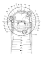
- FIG. 5 is a cross-sectional view showing a state in which the circuit unit is accommodated in the case.
- FIG. 6 is a plan view showing a state in which the circuit unit is accommodated in the case.
- the mounting board 62 is located with respect to the cylinder axis so that the front end 62a is located farther from the cylinder axis of the case 70 (coincides with the lamp axis J) than the rear end 62b. It is held by the case 70 in an inclined posture and in an arrangement that does not intersect the cylinder axis.
- the convex portion 66 of the mounting substrate 62 is fitted into the first positioning portion 74, and the rear end 63 a of the main body portion 63 of the mounting substrate 62 is fitted into the second positioning portion 77, so that It is held in an attitude that is inclined with respect to the cylinder axis and does not cross the cylinder axis.
- the lateral width W62a of the front side end 62a of the mounting substrate 62 is larger than the distance L74a between the lamp shaft J side edges of the first positioning portion 74 (the lateral width W62a and the distance L74a are parallel). Therefore, the front side end 62a does not move in the direction approaching the lamp axis J. Further, since the lateral width W62a is larger than the distance L74b between the edges of the first positioning portion 74 opposite to the lamp axis J (the lateral width W62a and the distance L74b are parallel), the front end 62a is separated from the lamp axis J. It doesn't move in the direction away from you.
- the lateral width W63a of the rear side end portion 63a of the main body portion 63 of the mounting substrate 62 is larger than the distance L75 between the projecting portions 75, the rear side end portion 62b does not move in the direction approaching the lamp axis J. Further, since the lateral width W63a is larger than the distance L76 between the rib portions 76, the rear side end portion 62b does not move in the direction away from the lamp axis J.
- the mounting substrate 62 can be stably supported in a posture inclined at a predetermined angle. Further, the mounting substrate 62 can be prevented from approaching and intersecting with the lamp axis J.
- the rear end 62b of the mounting substrate 62 is positioned at a position close to the lamp axis J. Thereby, the widest region in the case 70 can be effectively utilized, and the mounting substrate 62 having the lateral width of the rear side end portion 62b substantially the same as the inner diameter R of the large diameter portion 71 is accommodated in the case 70. Can do.
- the mounting substrate 62 is inclined so as to gradually move away from the lamp axis J from the rear side toward the front side, and the distance between the inner peripheral surfaces 71a of the case 70 becomes narrower as it goes away from the lamp axis J. In order to cope with this, the width of the mounting substrate 62 is designed to gradually narrow from the rear side toward the front side.
- the main body 63 of the mounting substrate 62 is accommodated in the large diameter portion 71 of the case 70, the connecting portion 65 is accommodated in the reduced diameter portion 73, and the distal end portion 64 is accommodated in the small diameter portion 72.
- the width of the main body 63 is designed to correspond to the inner diameter of the large diameter portion 71 of the case 70, the width of the connecting portion 65 corresponds to the inner diameter of the reduced diameter portion 73, and the width of the distal end portion 64 corresponds to the inner diameter of the small diameter portion 72. ing.
- the choke coil 61a, the electrolytic capacitor 61b, the capacitor 61c, the IC 61d, and the noise filter 61e mounted on the main body 63 are mainly housed in the large-diameter portion 71, and the resistance mounted on the connecting portion 65.
- 61 f is mainly accommodated in the small diameter portion 72.
- An electronic component may be mounted on the main surface 62d of the mounting substrate 62 opposite to the lamp axis J.
- the electronic components 61a to 61f mounted on the main surface 62c of the mounting substrate 62 on the lamp axis J side are the electrolytic capacitors 61b which are the tallest electronic components.
- the choke coil 61 a that is the second tallest electronic component is disposed in the region, and is disposed in the region on the rear side of the main body 63.
- the mounting substrate 62 has a posture as indicated by a two-dot chain line 100 by arranging the circuit units 60 vertically, the main surface 62c of the mounting substrate 62 on the lamp axis J side and the inner periphery of the large diameter portion 71 are disposed.
- the maximum gap width W1 with the surface 71a (the maximum value of the width in the direction perpendicular to the main surface 62c of the gap between the main surface 62c and the inner peripheral surface 71a) is substantially the same as the inner diameter of the large diameter portion 71.
- the maximum gap width W2 between the main surface 62c and the inner peripheral surface 71a is larger than the maximum gap width W1 in the case of the vertical arrangement. Therefore, the maximum gap width W2 between the main surface 62c and the inner peripheral surface 71a is larger than half of the inner diameter of the case 70. Therefore, a taller electronic component can be mounted on the main surface 62 c of the mounting substrate 62 than when the circuit unit 60 is arranged vertically.
- the height T1 (height from the main surface 62c) of the capacitor 61b is larger than the maximum gap width W1 and smaller than the maximum gap width W2.
- the main surface 62d of the mounting substrate 62 opposite to the lamp axis J is more specifically the surface of the pair of side end portions 63b of the main body 63 opposite to the lamp axis J of the rib portion 76. It is in contact with the inclined surface 76a. Thereby, the mounting substrate 62 can be stably held in a posture inclined at a predetermined angle.
- the inclined surface 76a also functions as a guide rail when the circuit unit 60 is accommodated in the case 70. Specifically, the circuit unit 60 can be smoothly inserted into a predetermined position in the case 70 by pressing the rear end 62b of the mounting board 62 against the inclined surface 76a and sliding on the inclined surface 76a. it can.
- the inclination angle of the inclined surface 76a with respect to the ramp axis J is preferably 3 to 15 ° in order to increase the maximum gap width W2. If the inclination angle is small, the maximum gap width W2 cannot be increased, and if the inclination angle is large, the mounting board 62 having a large lateral width cannot be accommodated inside the case 70.
- the vertical width (width in the direction orthogonal to the horizontal width direction) of the main body 63 of the mounting substrate 62 is larger than the length of the large diameter portion 71 of the case 70 in the direction along the lamp axis J. This is realized by inclining the mounting substrate 62.
- the mounting substrate 62 of the circuit unit 60 is held by the case 70 in an attitude that is inclined with respect to the cylindrical axis of the case 70 and does not intersect the cylindrical axis.
- the maximum gap width W2 between the main surface 62c on the cylinder axis side of the mounting substrate 62 and the inner peripheral surface 71a of the large-diameter portion 71 can be made larger than in the case of the vertical arrangement.
- the posture is inclined with respect to the cylinder axis so that the front end 62a of the mounting substrate 62 is located farther from the cylinder axis of the case 70 than the rear end 62b, the main surface on the cylinder axis side Wiring between the light emitting module 20 and the circuit unit 60 is easy because the state of the electronic components 61a to 61f and the like mounted on the 62c can be clearly seen from the opening 70a.
- the rear end 62 b of the mounting substrate 62 is close to the cylindrical axis of the case 70, a part of the mounting substrate 62 can be accommodated in the small diameter portion 72 of the case 70.
- the expression “does not intersect the cylinder axis” in the present application includes the meaning of “does not substantially intersect the cylinder axis but slightly intersects” in addition to the meaning “does not completely intersect the cylinder axis”. .
- the phrase “substantially intersects with the cylinder axis but slightly intersects” means that the main surface 62c on the lamp axis J side of the mounting substrate 62 slightly intersects with the cylinder axis (matches the lamp axis J).
- FIG. 7 is a cross-sectional view for explaining an arrangement in which the mounting substrate slightly intersects the cylinder axis, and electronic components and the like are omitted.
- the main surface 62c slightly intersects the lamp axis J, as shown in FIG. 7, in the cross section obtained by cutting the LED lamp 1 along a plane orthogonal to the main surface 62c and including the lamp axis J.
- the distance from the intersection P3 of the main surface 62c and the lamp shaft J to the rear side edge P2 is 20% or less with respect to the distance from the upper front side edge P1 to the rear side edge P2. Even when the main surface 62c slightly intersects the lamp axis J in this way, the effect of the present invention is achieved.
- the distance from the intersection P3 to the back side edge P2 is 10% or less with respect to the distance from the front side edge P1 to the back side edge P2, the effect of this invention will be more remarkable.
- the light source device according to the present invention has been specifically described above based on the embodiment.
- the light source device according to the present invention is not limited to the above-described embodiment, and for example, the following modifications may be considered. It is done.
- FIG. 8 is a cross-sectional view showing the accommodation state of the circuit unit of the light source device according to the modification.
- a circuit unit 160 is accommodated in the case 170 according to the modification.
- a pin type base 180 having a pair of pins 181 a and 181 b electrically connected to the circuit unit 160 is attached to the case 170.
- the circuit unit 160 is in a posture inclined with respect to the cylinder axis so that the rear end 162b is located farther from the cylinder axis of the case 170 (coincident with the lamp axis J) than the front end 162a.
- the electronic components 161a to 161f are mounted on the main surface 162c of the mounting substrate 162 on the lamp axis J side.
- the maximum gap width W2 can be made larger than when the circuit unit 160 is vertically arranged, a tall electronic component can be mounted on the main surface 162c of the mounting substrate 162. In this case, since the position of the maximum gap width W2 is on the base 180 side, a tall electronic component is disposed on the base 180 side.
- the light source device according to the present invention can be widely used in general lighting applications.
- Light source device 20 Light emitting module 60,160 Circuit unit 61a-61f, 161a-161f Electronic component 62,162 Mounting board 62a, 162a End part 62b, 162b near the opening 62c, 162c End part 62c, 162c Main surface 62d Main surface opposite to the cylinder axis 66 Projection 70, 170 Case 70a Opening 70b Open side end surface 71a Inner peripheral surface 74 First positioning portion 76a Inclined surface 77 Second positioning portion
Landscapes
- Engineering & Computer Science (AREA)
- Microelectronics & Electronic Packaging (AREA)
- General Engineering & Computer Science (AREA)
- Physics & Mathematics (AREA)
- Optics & Photonics (AREA)
- Non-Portable Lighting Devices Or Systems Thereof (AREA)
- Arrangement Of Elements, Cooling, Sealing, Or The Like Of Lighting Devices (AREA)
Abstract
Description
図1は、本実施形態に係る光源装置を示す斜視図である。図2は、本実施形態に係る光源装置を示す分解断面図である。
ボディ10は、前方側に開口11を有する椀状であって、後方から前方に向かって漸次拡径した略円筒状の筒部12と、筒部12の後方を閉塞する略円板状の底部13とを有する。筒部12の筒軸(ボディ10の筒軸でもある)は、ランプ軸Jと一致している。
発光モジュール20は、LEDランプ1の光源であって、モジュール基板21と、モジュール基板21の略中央に実装されたLEDユニット22とを備え、ボディ10内部における底部13上の略中央位置に搭載されている。LEDユニット22は、例えば、ユニット基板23と、ユニット基板23に実装された発光色が青色のInGaN系のLEDチップ24と、LEDチップ24を封止する黄緑色発光の蛍光体を含んだ略半球状の封止部25とを有し、前記LEDチップ24から発せられた青色光の一部を蛍光体によって黄緑色に色変換し、青色と黄緑色との混色により生じた白色光を出射する。
光学部材30は、例えば、透明アクリル樹脂などの透光性材料製であって、略円錐台形状のレンズ部31と、レンズ部31の周面に延設された略円環板状の外縁部32とを有し、それらレンズ部31と外縁部32とが一体に成形されている。
前面カバー40は、例えば、略円形状の光出射窓41を有する平板円環状の本体部42と、本体部42の外周縁から後方に向けて延出する短筒状の周壁部43とを備える。なお、前面カバー40の形状は上記に限定されず、ボディ10の開口11の形状に合わせてどのような形状であっても良い。
絶縁部材50は、回路ユニット60とボディ10との電気的な絶縁を図るためのものであって、樹脂、セラミック等の絶縁性の材料で形成されている。絶縁部材50は、ボディ10の底部13と略同径の略円板形状であって、底部13の後方に配置されている。
図3は、本実施形態に係る回路ユニットを示す斜視図である。図3に示すように、回路ユニット60は、例えば、商用電源から供給された交流電力を直流電力に整流する整流回路、および、整流回路により整流された直流電力の電圧値を調整する電圧調整回路などからなる点灯回路を含む。回路ユニット60は、口金80およびLEDユニット22と電気的に接続されており、口金80を介して照明器具(不図示)から受電し、LEDユニット22のLEDチップ24を発光させる。
図4は、本実施形態に係るケースおよび口金を示す断面斜視図である。図4に示すように、ケース70は、例えば前方側と後方側が開口した円筒形状であって、大径部71と、大径部71よりも外径および内径の小さい小径部72と、それら大径部71と小径部72とを連結する縮径部73とを有する。大径部71は前方側に、小径部72は後方側に位置しており、縮径部73は前方側から後方側に向かって漸次縮径している。
口金80は、LEDランプ1が照明器具に取り付けられ点灯された際に、照明器具のソケット(不図示)から電力を受けるための部材である。口金80の種類は、特に限定されるものではないが、本実施の形態ではエジソンタイプであるE11口金が使用されている。口金80は、略円筒形状であって外周面が雄ネジとなったシェル部81と、シェル部81に絶縁部82を介して装着されたアイレット部83とを備え、ケース70の小径部72に外嵌されている。
図2に示すように、ボディ10の底部13には、ねじ止めのための複数のねじ孔17と、配線のための配線孔(不図示)が設けられている。また、絶縁部材50にも、複数のねじ孔51と配線孔52とが設けられている。さらに、発光モジュール20のモジュール基板21にも複数のねじ孔26が設けられている。ねじ90が、モジュール基板21のねじ孔26、ボディ10のねじ孔17、および、絶縁部材50のねじ孔51に、その順で差し込まれ、さらにケース70のねじ孔78aにねじ込まれることによって、ボディ10、発光モジュール20、絶縁部材50およびケース70が一体に組み立てられている。
図5は、ケースへの回路ユニットの収容状態を示す断面図である。図6は、ケースへの回路ユニットの収容状態を示す平面図である。
以上、本発明に係る光源装置を実施の形態に基づいて具体的に説明してきたが、本発明に係る光源装置は、上記の実施の形態に限定されず、例えば以下のような変形例が考えられる。
20 発光モジュール
60,160 回路ユニット
61a~61f,161a~161f 電子部品
62,162 実装基板
62a,162a 開口に近い側の端部
62b,162b 開口に遠い側の端部
62c,162c 筒軸側の主面
62d 筒軸とは反対側の主面
66 凸部
70,170 ケース
70a 開口
70b 開口側の端面
71a 内周面
74 第1位置決め部
76a 傾斜面
77 第2位置決め部
Claims (7)
- 光源としての発光モジュールと、当該発光モジュールを点灯させるための複数の電子部品およびそれらが実装された実装基板を有する回路ユニットと、少なくとも一端に開口を有し内部に前記回路ユニットが収容された筒状のケースと、を備える光源装置であって、
前記実装基板は、前記ケースの筒軸に対して傾斜した姿勢で、且つ、前記筒軸と交差しない配置で、前記ケースにより保持されていることを特徴とする光源装置。 - 前記実装基板は、前記開口に近い側の端部が前記開口に遠い側の端部よりも前記筒軸から遠い位置に存在するよう、前記ケースにより保持されていることを特徴とする請求項1記載の光源装置。
- 前記ケースの内周面には、前記実装基板の前記開口に遠い側の端部を位置決めするための第1位置決め部が設けられていることを特徴とする請求項1または2に記載の光源装置。
- 前記ケースの内周面には、前記実装基板の前記開口に近い側の端部を位置決めするための第2位置決め部が設けられていることを特徴とする請求項1から3のいずれかに記載の光源装置。
- 前記第2位置決め部は、前記ケースの前記開口側の端面に形成され前記ケースの内部空間と連通する凹部であって、前記実装基板の前記開口に近い側の端部には、前記凹部内に嵌り込む凸部が設けられていることを特徴とする請求項4記載の光源装置。
- 前記ケースの内周面には、前記実装基板における前記筒軸とは反対側の主面を当接させるための傾斜面を有するリブ部が前記実装基板の傾斜に沿って形成されていることを特徴とする請求項1から5のいずれかに記載の光源装置。
- 前記ケースは円筒状であって、前記実装基板における前記筒軸側の主面と前記ケースの内周面との最大隙間幅は、前記ケースの内径の半分よりも大きいことを特徴とする請求項1から6のいずれかに記載の光源装置。
Priority Applications (4)
| Application Number | Priority Date | Filing Date | Title |
|---|---|---|---|
| JP2011554312A JP5028544B2 (ja) | 2011-01-14 | 2011-07-29 | 光源装置 |
| EP11817259A EP2503218A1 (en) | 2011-01-14 | 2011-07-29 | Light source device |
| US13/390,668 US20120243240A1 (en) | 2011-01-14 | 2011-07-29 | Light source apparatus |
| CN201180003517.0A CN102713415B (zh) | 2011-01-14 | 2011-07-29 | 光源装置 |
Applications Claiming Priority (2)
| Application Number | Priority Date | Filing Date | Title |
|---|---|---|---|
| JP2011006413 | 2011-01-14 | ||
| JP2011-006413 | 2011-01-14 |
Publications (1)
| Publication Number | Publication Date |
|---|---|
| WO2012095902A1 true WO2012095902A1 (ja) | 2012-07-19 |
Family
ID=46506835
Family Applications (1)
| Application Number | Title | Priority Date | Filing Date |
|---|---|---|---|
| PCT/JP2011/004345 Ceased WO2012095902A1 (ja) | 2011-01-14 | 2011-07-29 | 光源装置 |
Country Status (5)
| Country | Link |
|---|---|
| US (1) | US20120243240A1 (ja) |
| EP (1) | EP2503218A1 (ja) |
| JP (2) | JP5028544B2 (ja) |
| CN (1) | CN102713415B (ja) |
| WO (1) | WO2012095902A1 (ja) |
Cited By (2)
| Publication number | Priority date | Publication date | Assignee | Title |
|---|---|---|---|---|
| JP5285195B1 (ja) * | 2012-03-09 | 2013-09-11 | パナソニック株式会社 | ランプ |
| JP2015167115A (ja) * | 2014-03-04 | 2015-09-24 | パナソニックIpマネジメント株式会社 | 照明用光源及び照明装置 |
Families Citing this family (9)
| Publication number | Priority date | Publication date | Assignee | Title |
|---|---|---|---|---|
| JP2013251146A (ja) * | 2012-05-31 | 2013-12-12 | Funai Electric Co Ltd | 照明装置 |
| JP6288965B2 (ja) * | 2013-07-10 | 2018-03-07 | 三菱電機株式会社 | 照明装置用の収納部材及び照明装置 |
| USD738000S1 (en) * | 2013-08-15 | 2015-09-01 | Koninklijke Philips N.V. | LED par lamp |
| JP6497015B2 (ja) * | 2013-09-27 | 2019-04-10 | 三菱電機株式会社 | 照明ランプおよび照明装置 |
| US9435521B2 (en) * | 2014-05-21 | 2016-09-06 | Technical Consumer Products, Inc. | Antenna element for a directional lighting fixture |
| JP6452372B2 (ja) * | 2014-10-08 | 2019-01-16 | 三菱電機株式会社 | ランプ用の収納部材及びランプ及び照明装置 |
| USD794837S1 (en) * | 2014-10-13 | 2017-08-15 | GE Lighting Solutions, LLC | LED directional lamp with lens |
| DE102015202159B4 (de) | 2015-02-06 | 2023-06-15 | OSRAM Opto Semiconductors Gesellschaft mit beschränkter Haftung | Halbleiter-Beleuchtungsvorrichtung |
| CN110893816A (zh) * | 2019-12-09 | 2020-03-20 | 江苏丹帅车辆部件有限公司 | 一种农用车驾驶室顶棚灯 |
Citations (6)
| Publication number | Priority date | Publication date | Assignee | Title |
|---|---|---|---|---|
| JPS58103188U (ja) * | 1981-12-28 | 1983-07-13 | 三洋電機株式会社 | プリント基板の装着構造 |
| JPH087639A (ja) * | 1994-06-17 | 1996-01-12 | Matsushita Electric Works Ltd | 片持装着ランプ用ソケットアダプタ |
| JP2009087950A (ja) * | 2005-03-24 | 2009-04-23 | Toshiba Lighting & Technology Corp | 電球形蛍光ランプおよび照明装置 |
| JP2009163954A (ja) * | 2007-12-28 | 2009-07-23 | Sharp Corp | 取付体、それを備えてなる照明装置および取付方法 |
| JP2010129414A (ja) * | 2008-11-28 | 2010-06-10 | Toshiba Lighting & Technology Corp | 照明装置及び照明器具 |
| JP2010212073A (ja) | 2009-03-10 | 2010-09-24 | Toshiba Lighting & Technology Corp | 電球形蛍光ランプおよび照明装置 |
Family Cites Families (7)
| Publication number | Priority date | Publication date | Assignee | Title |
|---|---|---|---|---|
| US7847490B2 (en) * | 2005-03-24 | 2010-12-07 | Toshiba Lighting & Technology Corporation | Self-ballasted fluorescent lamp and lighting apparatus |
| US7758223B2 (en) * | 2005-04-08 | 2010-07-20 | Toshiba Lighting & Technology Corporation | Lamp having outer shell to radiate heat of light source |
| EP2163808B1 (en) * | 2007-05-23 | 2014-04-23 | Sharp Kabushiki Kaisha | Lighting device |
| KR100908136B1 (ko) * | 2007-12-27 | 2009-07-16 | 홍삼표 | Led 전구 |
| CN102175000B (zh) * | 2008-07-30 | 2013-11-06 | 东芝照明技术株式会社 | 灯装置及照明器具 |
| JP5218751B2 (ja) * | 2008-07-30 | 2013-06-26 | 東芝ライテック株式会社 | 電球型ランプ |
| US7965023B1 (en) * | 2010-03-17 | 2011-06-21 | Skynet Electronic Co., Ltd. | LED lamp |
-
2011
- 2011-07-29 JP JP2011554312A patent/JP5028544B2/ja active Active
- 2011-07-29 CN CN201180003517.0A patent/CN102713415B/zh not_active Expired - Fee Related
- 2011-07-29 WO PCT/JP2011/004345 patent/WO2012095902A1/ja not_active Ceased
- 2011-07-29 US US13/390,668 patent/US20120243240A1/en not_active Abandoned
- 2011-07-29 EP EP11817259A patent/EP2503218A1/en not_active Withdrawn
-
2012
- 2012-06-28 JP JP2012145227A patent/JP5416254B2/ja active Active
Patent Citations (6)
| Publication number | Priority date | Publication date | Assignee | Title |
|---|---|---|---|---|
| JPS58103188U (ja) * | 1981-12-28 | 1983-07-13 | 三洋電機株式会社 | プリント基板の装着構造 |
| JPH087639A (ja) * | 1994-06-17 | 1996-01-12 | Matsushita Electric Works Ltd | 片持装着ランプ用ソケットアダプタ |
| JP2009087950A (ja) * | 2005-03-24 | 2009-04-23 | Toshiba Lighting & Technology Corp | 電球形蛍光ランプおよび照明装置 |
| JP2009163954A (ja) * | 2007-12-28 | 2009-07-23 | Sharp Corp | 取付体、それを備えてなる照明装置および取付方法 |
| JP2010129414A (ja) * | 2008-11-28 | 2010-06-10 | Toshiba Lighting & Technology Corp | 照明装置及び照明器具 |
| JP2010212073A (ja) | 2009-03-10 | 2010-09-24 | Toshiba Lighting & Technology Corp | 電球形蛍光ランプおよび照明装置 |
Cited By (3)
| Publication number | Priority date | Publication date | Assignee | Title |
|---|---|---|---|---|
| JP5285195B1 (ja) * | 2012-03-09 | 2013-09-11 | パナソニック株式会社 | ランプ |
| WO2013132551A1 (ja) * | 2012-03-09 | 2013-09-12 | パナソニック株式会社 | ランプ |
| JP2015167115A (ja) * | 2014-03-04 | 2015-09-24 | パナソニックIpマネジメント株式会社 | 照明用光源及び照明装置 |
Also Published As
| Publication number | Publication date |
|---|---|
| CN102713415A (zh) | 2012-10-03 |
| EP2503218A1 (en) | 2012-09-26 |
| JP2012234820A (ja) | 2012-11-29 |
| JPWO2012095902A1 (ja) | 2014-06-09 |
| US20120243240A1 (en) | 2012-09-27 |
| JP5028544B2 (ja) | 2012-09-19 |
| CN102713415B (zh) | 2015-06-17 |
| JP5416254B2 (ja) | 2014-02-12 |
Similar Documents
| Publication | Publication Date | Title |
|---|---|---|
| JP5416254B2 (ja) | 光源装置 | |
| JP5015357B1 (ja) | 光源装置 | |
| CN102449382B (zh) | 灯以及照明装置 | |
| USRE47293E1 (en) | Illuminating apparatus | |
| EP2228587B1 (en) | Led bulb and lighting apparatus | |
| JP5320609B2 (ja) | ランプ装置および照明器具 | |
| JP6761968B2 (ja) | 照明装置 | |
| WO2012098594A1 (ja) | 光源装置 | |
| WO2013042238A1 (ja) | 電球形ledランプ | |
| JP2012195127A (ja) | Led照明装置 | |
| CN205424486U (zh) | 灯装置 | |
| JP4938916B1 (ja) | 光源装置 | |
| JP2012221636A (ja) | ランプ及び照明装置 | |
| JP2008300207A (ja) | 照明装置 | |
| CN206656166U (zh) | 灯装置以及照明装置 | |
| JP2017010885A (ja) | Led照明装置及び照明器具 | |
| CN203731340U (zh) | 灯 | |
| JP2014120412A (ja) | Ledランプ | |
| JP5477895B2 (ja) | Led照明装置 | |
| CN106287271A (zh) | 大角度球泡灯 | |
| JP6924963B2 (ja) | 照明器具 | |
| JP6288965B2 (ja) | 照明装置用の収納部材及び照明装置 | |
| CN107781711B (zh) | Led散热筒灯 | |
| JP2014146574A (ja) | ランプ及び照明装置 | |
| JP2020021691A (ja) | ランプ装置および照明装置 |
Legal Events
| Date | Code | Title | Description |
|---|---|---|---|
| WWE | Wipo information: entry into national phase |
Ref document number: 201180003517.0 Country of ref document: CN |
|
| WWE | Wipo information: entry into national phase |
Ref document number: 2011554312 Country of ref document: JP |
|
| WWE | Wipo information: entry into national phase |
Ref document number: 13390668 Country of ref document: US |
|
| WWE | Wipo information: entry into national phase |
Ref document number: 2011817259 Country of ref document: EP |
|
| 121 | Ep: the epo has been informed by wipo that ep was designated in this application |
Ref document number: 11817259 Country of ref document: EP Kind code of ref document: A1 |
|
| NENP | Non-entry into the national phase |
Ref country code: DE |