WO2012098622A1 - Condensateur du type à boîtier moulé - Google Patents
Condensateur du type à boîtier moulé Download PDFInfo
- Publication number
- WO2012098622A1 WO2012098622A1 PCT/JP2011/007188 JP2011007188W WO2012098622A1 WO 2012098622 A1 WO2012098622 A1 WO 2012098622A1 JP 2011007188 W JP2011007188 W JP 2011007188W WO 2012098622 A1 WO2012098622 A1 WO 2012098622A1
- Authority
- WO
- WIPO (PCT)
- Prior art keywords
- pole
- bus bar
- block
- case
- pole bus
- Prior art date
- Legal status (The legal status is an assumption and is not a legal conclusion. Google has not performed a legal analysis and makes no representation as to the accuracy of the status listed.)
- Ceased
Links
Images



Classifications
-
- H—ELECTRICITY
- H01—ELECTRIC ELEMENTS
- H01G—CAPACITORS; CAPACITORS, RECTIFIERS, DETECTORS, SWITCHING DEVICES, LIGHT-SENSITIVE OR TEMPERATURE-SENSITIVE DEVICES OF THE ELECTROLYTIC TYPE
- H01G4/00—Fixed capacitors; Processes of their manufacture
- H01G4/002—Details
- H01G4/224—Housing; Encapsulation
-
- H—ELECTRICITY
- H01—ELECTRIC ELEMENTS
- H01G—CAPACITORS; CAPACITORS, RECTIFIERS, DETECTORS, SWITCHING DEVICES, LIGHT-SENSITIVE OR TEMPERATURE-SENSITIVE DEVICES OF THE ELECTROLYTIC TYPE
- H01G2/00—Details of capacitors not covered by a single one of groups H01G4/00-H01G11/00
- H01G2/02—Mountings
- H01G2/04—Mountings specially adapted for mounting on a chassis
-
- H—ELECTRICITY
- H01—ELECTRIC ELEMENTS
- H01G—CAPACITORS; CAPACITORS, RECTIFIERS, DETECTORS, SWITCHING DEVICES, LIGHT-SENSITIVE OR TEMPERATURE-SENSITIVE DEVICES OF THE ELECTROLYTIC TYPE
- H01G4/00—Fixed capacitors; Processes of their manufacture
- H01G4/002—Details
- H01G4/228—Terminals
-
- H—ELECTRICITY
- H01—ELECTRIC ELEMENTS
- H01G—CAPACITORS; CAPACITORS, RECTIFIERS, DETECTORS, SWITCHING DEVICES, LIGHT-SENSITIVE OR TEMPERATURE-SENSITIVE DEVICES OF THE ELECTROLYTIC TYPE
- H01G4/00—Fixed capacitors; Processes of their manufacture
- H01G4/38—Multiple capacitors, i.e. structural combinations of fixed capacitors
-
- Y—GENERAL TAGGING OF NEW TECHNOLOGICAL DEVELOPMENTS; GENERAL TAGGING OF CROSS-SECTIONAL TECHNOLOGIES SPANNING OVER SEVERAL SECTIONS OF THE IPC; TECHNICAL SUBJECTS COVERED BY FORMER USPC CROSS-REFERENCE ART COLLECTIONS [XRACs] AND DIGESTS
- Y02—TECHNOLOGIES OR APPLICATIONS FOR MITIGATION OR ADAPTATION AGAINST CLIMATE CHANGE
- Y02T—CLIMATE CHANGE MITIGATION TECHNOLOGIES RELATED TO TRANSPORTATION
- Y02T10/00—Road transport of goods or passengers
- Y02T10/60—Other road transportation technologies with climate change mitigation effect
- Y02T10/70—Energy storage systems for electromobility, e.g. batteries
Definitions
- the present invention relates to a case mold type capacitor in which a metallized film capacitor is resin-molded in a case.
- the present invention relates to a case mold type capacitor that is used in various electronic devices, electrical devices, industrial devices, automobiles, and the like, and that is optimal for smoothing, filtering, and snubber of an inverter circuit for driving a motor of a hybrid vehicle.
- HEVs hybrid vehicles
- metallized film capacitors with a very long life to be used for such HEVs from the demand for maintenance-free in the market.
- the working voltage range of the electric motor used for HEV is as high as several hundred volts. Therefore, there is a strong demand for a metallized film capacitor having a high withstand voltage, capable of charging / discharging with a large current, a large capacity, and a low loss at a high withstand voltage.
- a case mold type capacitor has been developed and put into practical use in which a plurality of metallized film capacitors connected in parallel by a bus bar are housed in a case, and a mold resin is injected into the case and fixed. ing.
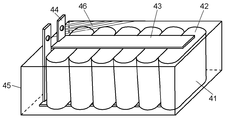
- Fig. 7 shows the configuration of a conventional case mold type capacitor.
- This case mold type capacitor includes a plurality of capacitor elements 41, a pair of bus bars 43, and a case 45.
- the capacitor element 41 is formed by winding two metallized films formed by vapor-depositing metal on one side of a polypropylene film that is a dielectric, in a flat shape.
- Metallicon electrode portions 42 as electrodes are provided at both ends in the width direction of the metallized film of each capacitor element 41.
- the metallicon electrode portion 42 is formed by zinc spraying.
- a pair of elongated copper bus bars 43 connect the metallicon electrode portions 42 at both ends of the plurality of capacitor elements 41.
- Each bus bar 43 has an electrode terminal 44 connected to the outside, and is integrally formed by bending.
- Case 45 is made of polyphenylene sulfide.
- the plurality of capacitor elements 41 are closely arranged in a row in the case 45 with the flat surfaces facing the same direction.
- Metallicon electrode portions 42 at both ends of each capacitor element 41 are positioned substantially in the same plane, and one of the metallicon electrode portions 42 is disposed on the opening surface side of the case 45 and the other is disposed on the bottom surface side.
- the pair of bus bars 43 connect the metallicon electrode portions 42 located on the opening surface side and the bottom surface side of the case 45, respectively.
- the electrode terminal 44 is disposed outside the case 45.
- the empty space in the case 45 containing the plurality of capacitor elements 41 and the pair of bus bars 43 is filled with an epoxy resin 46 (only a part thereof is indicated by hatching in the drawing) as a sealing material, and is moisture resistant. Etc., and the reliability is improved.
- FIG. 8 shows a configuration in which a plurality of metallized film capacitors are arranged in parallel and the electrodes of the capacitor elements are connected to the bus bars.
- Each capacitor element 1 has end face electrodes 2 at both ends.
- the capacitor element 1 is a film capacitor, and the end face electrode 2 is formed of a metallicon.
- Three capacitor elements 1 are juxtaposed in a direction orthogonal to the arrangement direction of the pair of end face electrodes 2 in each capacitor element 1 to form a capacitor element array 10A.
- a capacitor element group 10C is formed by arranging capacitor element rows 10B having the same structure as described above adjacent to each other in the arrangement direction of the pair of end face electrodes 2 in each capacitor element 1 of the capacitor element row 10A. .
- the first flat plate electrode 11 is disposed substantially parallel to the arrangement direction (arrangement surface) of the capacitor element 1.
- a second flat plate electrode 12 is disposed outside the first flat plate electrode 11 (on the side opposite to the capacitor element group 10 ⁇ / b> C) substantially in parallel with the first flat plate electrode 11.
- Each of the first flat plate electrode 11 and the second flat plate electrode 12 is a rectangular plate made of copper, and is provided with openings 13 and 14 that are square and extend along the capacitor element rows 10A and 10B, respectively, at the center thereof. .
- the opening 13 of the first flat plate electrode 11 is formed to be larger in width and length than the opening 14 of the second flat plate electrode 12.
- the end face electrode 2 located inside the capacitor element rows 10A and 10B is connected to the periphery of the opening 14 of the second plate electrode 12 through the opening 13 of the first plate electrode 11 by the lead terminal 3B. Further, the end face electrodes 2 positioned outside the capacitor element arrays 10A and 10B are connected to both outer side portions (side end portions) of the first flat plate electrode 11 by lead terminals 3A.
- the lead terminals 3A and 3B for example, copper tape can be used, and the length is preferably about several mm (10 mm or less), and the inductance is preferably as small as possible.
- the lead terminals 3A and 3B may be formed integrally with the end face electrode 2. With the above connection structure, all the capacitor elements 1 in the capacitor element group 10 ⁇ / b> C are connected in parallel between the first plate electrode 11 and the second plate electrode 12.
- Insulating paper or insulating film (not shown) is inserted between the capacitor element group 10 ⁇ / b> C and the first flat plate electrode 11 and between the first flat plate electrode 11 and the second flat plate electrode 12.
- the capacitor element group 10C, the first plate electrode 11, and the second plate electrode 12 can be arranged as close as possible.
- the structure thus configured is housed in a case and sealed with a resin such as an epoxy resin to form a case mold type capacitor.
- the capacitance of the constructed capacitor is several hundred ⁇ F to several thousand ⁇ F, and the inductance is several nH to several tens nH, which is useful for a smoothing capacitor of an inverter.
- This capacitor has excellent mechanical strength, heat resistance, water resistance and high reliability by molding the capacitor element group 10C in a case with a molding resin.
- a case mold type capacitor is disclosed in Patent Document 2, for example.
- the case mold type capacitor shown in FIG. 7 cannot satisfy the electrical characteristics of high withstand voltage and low loss when used for HEVs or electric vehicles.
- the thickness of the mold resin is increased, and there is a possibility that cracks and cracks may occur in the capacitor case and the mold resin due to the influence of thermal shock assumed in automotive applications.
- the case mold type capacitor shown in FIG. 8 satisfies the electrical characteristics of high withstand voltage and low loss.
- the connection between the end face electrode 2 of the capacitor element 1 and the plate electrodes 11 and 12 is complicated.
- the lead terminal 3 ⁇ / b> B connects the end face electrode 2 positioned inside through the opening 13 of the first flat plate electrode 11 to the periphery of the opening 14 of the second flat plate electrode 12. Therefore, there is a problem in the reliability of insulation between the end face electrode 2, the lead terminal 3 ⁇ / b> B, and the first flat plate electrode 11.
- the width of the metallized film of the two or more types of capacitors must be substantially the same size. I must. Due to this restriction, it is difficult to select optimal performance and shape for each function of two or more types of capacitors.
- JP 2004-186640 A Japanese Patent Laid-Open No. 2005-005467
- capacitors when two or more types of capacitors are housed in one case and resin molded, it is excellent in electrical characteristics with high withstand voltage and low loss, and can be designed with low cost, small size and light weight and high efficiency.
- a case mold type capacitor is provided.
- the case mold type capacitor of the present invention includes first and second blocks made of metallized film capacitors, first and second P pole bus bars, first and second N pole bus bars, a case, a mold resin, Have Each metallized film capacitor has a P pole and an N pole.
- the first P pole bus bar is connected to the P pole of the metallized film capacitor in the first block, and has a first P pole terminal part for external connection at one end.
- the first N pole bus bar is connected to the N pole of the metallized film capacitor in the first block, and has a first N pole terminal portion for external connection at one end.
- the second P pole bus bar is connected to the P pole of the metallized film capacitor in the second block, and has a second P pole terminal portion for external connection at one end.
- the second N pole bus bar is connected to the N pole of the metallized film capacitor in the second block, and has a second N pole terminal portion for external connection at one end.
- the case has an opening at the top and accommodates the first and second blocks.
- the mold resin has the first and second blocks, the first P pole bus bar, the first N pole bus bar, the first P pole terminal portion, the first N pole terminal portion, the second P pole terminal portion, and the second N pole terminal portion exposed.
- a second P-pole bus bar and a second N-pole bus bar are embedded.
- the P pole of the metallized film capacitor in the first block faces the P pole of the metallized film capacitor in the second block.
- the N pole of the metalized film capacitor in the first block and the N pole of the metalized film capacitor in the second block are opposed to each other.
- the first P-pole terminal portion and the second P-pole terminal portion are connected, and the first N-pole terminal portion and the second N-pole terminal portion are connected.
- the first P-pole bus bar, the first N-pole bus bar, the second P-pole bus bar, and the second N-pole bus bar have portions located on the opening side of the case with respect to the first block and the second block.
- the first P-pole bus bar and the second P-pole bus bar partially overlap, and the first N-pole bus bar and the second N-pole bus bar partially overlap.
- the bus bar is not unnecessarily lengthened, and the resistance for each block can be kept low.
- the capacity can be increased and the withstand voltage can be increased, and furthermore, low loss electric characteristics can be realized. Therefore, even in the bus bar design, there is no excessive design with respect to the current-resistant design, and the size and weight can be reduced. Further, by using the two bus bars that are overlapped, heat generated in the bus bar during actual use can be efficiently radiated.
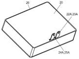
- FIG. 1A is a perspective view of a case mold type capacitor according to an embodiment of the present invention.
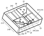
- FIG. 1B is a perspective view of the case mold type capacitor shown in FIG. 1A before injecting mold resin.
- FIG. 2 is a perspective view of the case mold type capacitor shown in FIG. 1A before the case is inserted.
- FIG. 3 is a graph showing the change with time of the capacitance ratio of the case mold type capacitor shown in FIG. 1A.
- FIG. 4 is a graph showing the change with time of the loss rate of the case mold type capacitor shown in FIG. 1A.
- FIG. 5 is a perspective view showing a configuration of a capacitor block of a comparative example for comparison with the embodiment of the present invention.
- FIG. 6 is a perspective view of another case mold type capacitor according to the embodiment of the present invention before injecting mold resin.
- FIG. 7 is a perspective view showing a configuration of a conventional case mold type capacitor.
- FIG. 8 is a perspective view showing the configuration of another conventional case mold type capacitor.
- FIG. 1A is a perspective view of a case mold type capacitor according to an embodiment of the present invention
- FIG. 1B is a perspective view before a mold resin is injected
- FIG. 2 is a perspective view of the case mold type capacitor shown in FIG. 1A before the case is inserted.
- the case mold type capacitor includes a first block 21A, a first P pole bus bar 22, a first N pole bus bar 24, a second block 21B, a second P pole bus bar 23, A second N pole bus bar 25 and a case 26 are provided.
- the case mold type capacitor further includes a mold resin 20.
- the first block 21A and the second block 21B are composed of a plurality of metallized film capacitors (hereinafter referred to as capacitors) 21 each having a P pole and an N pole.
- capacitors 21 metallized film capacitors
- Each of the first block 21A and the second block 21B may be composed of one capacitor 21.
- the N pole of each capacitor 21 in the block 21A faces the N pole of each capacitor 21 in the block 21B.
- the first P pole bus bar (hereinafter referred to as P pole bus bar) 22 is connected to the P pole of the capacitor 21 in the block 21A, and has a first P pole terminal portion (hereinafter referred to as P pole terminal portion) 22A for external connection at one end.
- the first N pole bus bar (hereinafter referred to as N pole bus bar) 24 is connected to the N pole of the capacitor 21 in the block 21A, and has a first N pole terminal portion (hereinafter referred to as N pole terminal portion) 24A for external connection at one end. .
- the second P pole bus bar (hereinafter referred to as P pole bus bar) 23 is connected to the P pole of the capacitor 21 in the block 21B, and has a second P pole terminal portion (hereinafter referred to as P pole terminal portion) for external connection at one end. 23A.
- the second N pole bus bar (hereinafter referred to as N pole bus bar) 25 is connected to the N pole of capacitor 21 in block 21B, and has a second N pole terminal portion (hereinafter referred to as N pole terminal portion) 25A for external connection at one end. .
- the case 26 has an opening at the top and accommodates the blocks 21A and 21B.
- the P-pole bus bars 22 and 23 and the N-pole bus bars 24 and 25 have portions located on the opening side of the case 26 with respect to the first block 21A and the second block 21B.
- the mold resin 20 is filled in the case 26, and the blocks 21A and 21B, the P pole bus bars 22 and 23, and the N pole bus bar 24 are exposed so that the P pole terminal portions 22A and 23A and the N pole terminal portions 24A and 25A are exposed. , 25 are buried.
- the capacitor 21 has a flat shape, and a pair of end surfaces 21P and 21N provided with a P-pole and an N-pole, respectively, and a pair of flat main surfaces 21F connecting the end surfaces 21P and 21N, and A pair of curved surfaces 21R.
- the plurality of capacitors 21 are linearly arranged such that the upper main surface 21F and the lower main surface 21F are on the same plane.
- the capacitor 21 is composed of a pair of metallized films in which a metal vapor-deposited electrode is formed on one or both sides of polypropylene, which is a dielectric film. These metal vapor deposition electrodes are wound in a state of facing each other with a dielectric film interposed therebetween. Metallicon electrodes sprayed with zinc are formed on both end faces. Each metallicon electrode constitutes a P-electrode and an N-electrode extraction electrode.
- the P-pole bus bar 22 is formed by punching a metal plate into a substantially L shape and bending it. One end of the P-pole bus bar 22 is provided with a joint (not shown) to be joined to the P-pole of the capacitor 21, and the other end is provided with a P-pole terminal part 22 ⁇ / b> A, and the central part is planar. .
- the central portion means a portion excluding a joint portion to be joined to the P pole of the capacitor 21, the P pole terminal portion 22A, and a first P pole terminal reinforcing portion 22B described later.
- the central portion of the P-pole bus bar 22 is disposed so as to be positioned above the blocks 21A and 21B (on the opening side of the case 26).
- tongue-shaped soldering portions (not shown) formed so as to branch from the joint portion are provided at two locations.
- the soldering part is joined to the P pole by soldering.
- the P-pole terminal portion 22A is drawn above the capacitor 21 and exposed from the mold resin 20 in the case 26.
- the N pole bus bar 24 is also formed by punching a metal plate into a substantially L shape and bending it. One end of the N pole bus bar 24 is provided with a junction (not shown) to be joined to the N pole of the capacitor 21, and the other end is provided with an N pole terminal portion 24 ⁇ / b> A, and the central portion is planar. . The central portion of the N-pole bus bar 24 is disposed so as to be positioned above the block 21B (on the opening side of the case 26).
- tongue-like soldering portions (not shown) formed so as to branch from the joint portion are provided at two locations.
- the soldering part is joined to the N pole by soldering.
- the N-pole terminal portion 24 ⁇ / b> A is pulled out above the capacitor 21 and is exposed from the mold resin 20 in the case 26.
- the P pole bus bar 23 is joined to the P pole of the capacitor 21, and the N pole bus bar 25 is joined to the N pole.
- the P pole bus bar 23 is formed by punching a metal plate into a square shape and processing it.
- a junction (not shown) to be joined to the P pole of the capacitor 21 is provided at the end of the rectangular shape in the longitudinal direction, and a P pole terminal portion 23A is provided at the other end.
- tongue-like soldering portions (not shown) formed so as to branch from the joint portion are provided at two locations. The soldering portions are respectively joined to the P pole by soldering, and the P pole terminal portion 23A is exposed from the mold resin 20 in the case 26.
- the N pole bus bar 25 is formed by punching a metal plate into a substantially L shape and bending it. A joint (not shown) joined to the N pole is provided at one end, and an N pole terminal is provided at the other end. A portion 25A is provided. The flat central portion is disposed so as to be positioned on the upper portion of the block 21B (on the opening side of the case 26).
- tongue-like soldering portions (not shown) formed so as to branch from the joint portion are provided at two locations.
- the soldering portions are respectively joined to the N pole by soldering, and the N pole terminal portion 25A is pulled out above the capacitor 21 and exposed from the mold resin in the case 26.
- the P pole terminal portion 22A and the P pole terminal portion 23A are connected, and the N pole terminal portion 24A and the N pole terminal portion 25A are connected. More specifically, the P-pole terminal portion 22A and the P-pole terminal portion 23A are overlapped and joined when exposed from the case 26 to constitute a P-pole external connection terminal. On the other hand, the planar central portions of the N pole bus bars 24 and 25 are overlapped on the upper portion of the block 21B (the opening side of the case 26). Also, the N pole terminal portion 24A and the N pole terminal portion 25A are overlapped and joined when exposed from the case 26, thereby constituting an N pole external connection terminal.
- a plurality of metallized film capacitors 21 are divided into blocks 21A and 21B.
- Each bus bar has a portion arranged on the opening side of the case 26 with respect to the blocks 21A and 21B, and extends to the terminal portion at the shortest distance. Therefore, the bus bar is not unnecessarily lengthened, and the resistance for each block can be kept low.
- the metallized film capacitor 21 the capacity of the case mold type capacitor can be increased, the withstand voltage can be increased, and the low loss electric characteristics can be realized. Therefore, even in the bus bar design, there is no excessive design with respect to the withstand current design, and the case mold type capacitor can be reduced in size and weight.
- the inductances of the divided blocks 21A and 21B become substantially equal. Further, the N pole bus bars 24 and 25 are overlapped to form one terminal portion for external connection. Therefore, the heat generation of the N pole bus bars 24 and 25 is halved, and the temperature of the capacitor 21 rises abnormally even if the N pole bus bars 24 and 25 are arranged on the top of the capacitor 21 and the terminals for external connection are pulled out from the same direction. The cost can be reduced without doing so.
- the blocks 21A and 21B are connected with the P pole of the capacitor 21 on the outside and the N pole on the inside, but the present invention is not limited to this, and the P pole is arranged on the inside. Also good. That is, the P pole of each capacitor 21 in the block 21A may be opposed to the P pole of the capacitor 21 in the block 21B. In this case, the first and second P pole bus bars may be overlapped to form one external connection terminal portion.
- the blocks 21A and 21B are configured by using a plurality of flat capacitors 21.
- the capacitors 21 are preferably arranged linearly so that the main surfaces 21F are on the same plane. With this arrangement, the yield can be improved and the cost can be reduced. Further, since the heat dissipation is improved by arranging the main surface 21F of the capacitor 21 in parallel with the bottom surface of the case 26, it is possible to realize a large capacity and low loss electric characteristics with high withstand voltage. . Further, the main surface 21 ⁇ / b> F, which is a flat surface of the capacitor 21, is disposed in parallel with the bottom surface of the case 26, so that the height can be reduced.
- the planar central portions of the N-pole bus bar 24 and the N-pole bus bar 25 are superposed on the upper part of the block 21B of the capacitor 21 (opening side of the case 26).
- the N-pole terminal portion 24A and the N-pole terminal portion 25A are overlapped and joined when exposed from the case 26, and constitute an N-pole external connection terminal. Therefore, in order to shorten the current path of the N-pole bus bars 24 and 25 and keep the resistance low, the N-pole bus bar 24 and the N-pole bus bar 25 inevitably partially overlap at the upper part of the block 21B. Since the flat central portion has a relatively wide shape, heat generated in the N-pole bus bar 24 and the N-pole bus bar 25 during actual use can be efficiently radiated.
- the N pole bus bar 25 located on the capacitor 21 side of the two overlapping bus bars on the upper surface of the capacitor 21, that is, the surface on the opening side of the case 26, is the opening of the case 26.
- the area of the planar central portion is larger than that of the N-pole bus bar 24 located on the part side.
- the central portion of the N pole bus bar 24 is formed in a substantially triangular shape, whereas the central portion of the N pole bus bar 25 is obtained by adding a trapezoidal plane to the oblique side portion of the substantially triangular shape. It has a shape.
- the N pole bus bars 24 and 25 are configured in this way, the trapezoidal planar portion of the N pole bus bar 25 described above is not covered with the N pole bus bar 24. That is, part of the N pole bus bar 25 is exposed from the N pole bus bar 24 to the opening side of the case 26 before the case 26 is filled with the mold resin before curing.
- the mold resin 20 when the mold resin 20 is filled in the case 26, the mold resin 20 easily flows from the trapezoidal flat portion of the N pole bus bar 25 into the gap between the N pole bus bar 24 and the N pole bus bar 25. . Therefore, it can suppress that the part which is not filled with the mold resin 20 between the N pole bus bar 24 and the N pole bus bar 25 generate
- the P-pole bus bars overlap each other. That is, it is preferable that at least a part of the bus bars near the blocks 21A and 21B among the first and second P-pole bus bars are exposed from the other bus bar to the opening side of the case 26.
- the other bus bar is a bus bar located on the opening side of the case 26 of the P-pole bus bars 22 and 23.
- the N pole bus bar 24 is preferably provided with three first through holes (hereinafter referred to as through holes) 24C, 24D, and 24E.
- through holes three first through holes (hereinafter referred to as through holes) 24C, 24D, and 24E.
- the through holes 24C, 24D, and 24E are preferably circular.
- the mold resin 20 can easily enter the through holes 24C, 24D, and 24E as compared with a case where a polygonal hole is provided.
- the mold resin 20 can easily enter the through holes 24C, 24D, and 24E as compared with a case where a polygonal hole is provided.
- three through holes are provided, but the number is not limited to this.
- the upper surface of the N pole bus bar 25 faces the opening side of the case 26 from the through holes 24 ⁇ / b> C and 24 ⁇ / b> D of the N pole bus bar 24 before the case 26 is filled with the mold resin 20. It is in an exposed state. Therefore, when filling the case 26 with the mold resin 20, the mold resin 20 that has entered the through holes 24 ⁇ / b> C and 24 ⁇ / b> D first comes into contact with the upper surface of the N pole bus bar 25, and from there, the N pole bus bar 24 and the N pole bus bar 25. It gradually expands into the gap between the two. As a result, the mold resin 20 is sufficiently filled also between the N pole bus bar 24 and the N pole bus bar 25.
- the first through hole is provided in the bus bar located on the opening side of the case 26 among the first and second P-pole bus bars.
- the bus bar close to the blocks 21A and 21B is preferably exposed to the opening side of the case 26 from the first through hole.
- the N pole bus bar 25 is provided with a second through hole (hereinafter referred to as a through hole) 25C at a position below the through hole 24E. That is, the through hole 24E and the through hole 25C are overlapped and connected. Therefore, the space above the N pole bus bar 24 and the space below the N pole bus bar 25 are in communication with each other via the through holes 24E and 25C. As described above, the capacitor 21 is exposed from the through holes 24 ⁇ / b> E and 25 ⁇ / b> C toward the opening of the case 26 before the mold resin 20 is filled in the case 26.
- the mold resin 20 before curing is filled in the case 26
- the mold resin 20 passes through the through holes 24 ⁇ / b> E and 25 ⁇ / b> C and wraps around the gap between the N-pole bus bar 25 and the capacitor 21.
- the mold resin 20 can be sufficiently filled in the case 26.
- the through hole 25C is desirably smaller than the through hole 24E.
- a part of the N pole bus bar 25 is exposed from the through hole 24 ⁇ / b> E toward the opening side of the case 26.
- a part of the mold resin 20 that has entered the through-hole 24E comes into contact with the upper surface of the N-pole bus bar 25 exposed from the above-described through-hole 24E, and further, there is a gap between the N-pole bus bar 24 and the N-pole bus bar 25. It is possible to extend to.
- the through-hole 25C of the N-pole bus bar 25 and the through-hole 24E of the N-pole bus bar 24 are provided between the adjacent capacitors 21.
- the 2nd through-hole is provided in the position which overlaps with a 1st through-hole in the bus bar near blocks 21A and 21B among the 1st and 2nd P pole bus bars.
- the second through hole is more preferably smaller than the first through hole.
- the second through hole is preferably provided between two adjacent capacitors 21.
- the capacitor 21 has a flat shape and includes a main surface 21F and a pair of curved surfaces 21R provided on both the left and right sides of the main surface 21F.
- the curved surfaces 21R of the adjacent capacitors 21 are in contact with each other or face each other. That is, between the capacitors 21 provided with the above-described through holes 25 ⁇ / b> C is a position above the curved surfaces 21 ⁇ / b> R of the adjacent capacitors 21. If the through-hole 25C is arranged at a position where even a part of the curved surface 21R is exposed from the through-hole 25C in the state before filling with the mold resin 20, it is surrounded by the adjacent capacitors 21 and the N-pole bus bar 25. The remaining space can be filled with mold resin.
- a part of the main surface 21F of the capacitor 21 and a part of the curved surface 21R are exposed toward the opening of the case 26 from the through hole 25C.
- a part of the mold resin 20 that has entered the through hole 25C comes into contact with the upper surface (main surface 21F) of the capacitor 21, and further, between the N-pole bus bar 25 and the upper surface of the capacitor 21. It spreads in the gap.
- the remaining mold resin 20 that has entered the through hole 25C fills the space surrounded by the adjacent capacitors 21 and the N-pole bus bar 25. Therefore, by arranging the through-hole 25C in this way, it is possible to fill the case 26 more efficiently without leaving the interior of the case 26.
- FIG. 2 is a perspective view in which the P pole bus bars 22 and 23 and the N pole bus bars 24 and 25 are joined to the blocks 21A and 21B.
- the P-pole bus bar 22 is disposed so as to be located above the blocks 21A and 21B of the capacitor 21 (on the opening side of the case 26).
- a first P pole terminal reinforcing portion 22B is provided in front of the P pole terminal portion 22A for external connection of the P pole bus bar 22, and a second P pole terminal reinforcing portion is also provided in front of the P pole terminal portion 23A of the P pole bus bar 23. 23B is provided.
- the P-pole bus bar 22 has a P-pole terminal reinforcing part 22B adjacent to the P-pole terminal part 22A
- the P-pole bus bar 23 has a P-pole terminal reinforcing part 23B adjacent to the P-pole terminal part 23A.
- the N-pole bus bar 24 is disposed so as to be positioned above the block 21B of the capacitor 21 (on the opening side of the case 26).
- a first N pole terminal reinforcing portion 24B is provided in front of the N pole terminal portion 24A for external connection of the N pole bus bar 24, and a second N pole terminal reinforcing portion 25B is also provided in front of the N pole terminal portion 25A of the N pole bus bar 25. Is provided. That is, it is preferable that the N pole bus bar 24 has an N pole terminal reinforcing portion 24B adjacent to the N pole terminal portion 24A, and the N pole bus bar 25 has an N pole terminal reinforcing portion 25B adjacent to the N pole terminal portion 25A.
- the P-pole terminal portions 22A and 23A are overlapped and joined as described above to form an external connection terminal.
- a substantially triangular gap is provided in the penetrating direction between the P-pole terminal reinforcing portion 22B and the P-pole terminal reinforcing portion 23B adjacent to the external connection terminal.
- a substantially triangular gap is also provided in the penetrating direction between the N pole terminal reinforcing portion 24B and the N pole terminal reinforcing portion 25B.
- the P-pole terminal portions 22A and 23A and the N-pole terminal portions 24A and 25A can be firmly fixed by the mold resin 20. Therefore, even if an external connection terminal is connected to an external component, the interface between the P-pole terminal portions 22A and 23A and the N-pole terminal portions 24A and 25A and the mold resin 20 is not damaged, and the life is extended. Can do.
- the gap between the P-pole terminal reinforcing portion 22B and the P-pole terminal reinforcing portion 23B and the gap between the N-pole terminal reinforcing portion 24B and the N-pole terminal reinforcing portion 25B are projected at least 2 mm from the interface with the mold resin 20.
- the required protrusion height depends to some extent on the width and thickness of the terminal reinforcing portion and the viscosity of the mold resin 20 before curing.
- the width of the terminal reinforcing portion is 15 mm
- the thickness is 0.6 mm
- the viscosity of the mold resin 20 is In the case of about 4000 mPa ⁇ s, it may be 2 mm or more.
- the shape of the gap in the penetration direction may be a square shape or a polygonal shape, and the smallest dimension of the gap is a dimension of at least 2 mm in the space formed at the interface between the two terminal reinforcing portions and the mold resin 20. I just need it.
- a case mold type capacitor is formed as shown in FIGS. 1A and 2 using six cells of a metallized film capacitor having a rated voltage of 600 VDC and a capacity of 400 ⁇ F.
- the rated voltage of the case mold type capacitor is 600 VDC
- the capacity is 2400 ⁇ F
- it is used at an ambient temperature of ⁇ 40 ° C. to 90 ° C. and a high frequency ripple current of 70 to 100 A.
- FIG. 3 shows the measurement results of the capacitance change rate of the capacitor 21 when the case mold type capacitor was subjected to an acceleration test by energizing a sinusoidal ripple current 100 A (frequency 20 kHz) for 1000 hours in a 90 ° C. atmosphere.
- the measurement results are shown in FIG.
- the results of the surface temperature of the capacitor 21 during the acceleration test are shown in (Table 1).
- FIG. 1 The configuration of the case mold type capacitor of the comparative example is shown in FIG.
- blocks 27A and 27B are formed by arranging six capacitors 21 as in the configuration shown in FIG.
- the outside of the blocks 27A and 27B is the P pole and the center side is the N pole, which are connected by the P pole bus bar 28 and the N pole bus bar 29, respectively.
- the capacitor connection body configured as described above is molded with the case 26 and the mold resin 20 in the same manner as the present embodiment.
- the case mold type capacitor according to the present embodiment has an improved capacity change rate and loss rate after 1000 hours as compared with the comparative example.
- the root portion (location B) of each electrode terminal portion where the surface temperature is highest is 12 ° C. lower than the comparative example. Accordingly, the heat damage of the capacitor 21 is reduced, and it is possible to provide a case-molded capacitor capable of realizing large capacity, low loss electrical characteristics with high withstand voltage, and capable of being reduced in size and weight. .
- the P-pole bus bar 22 is disposed so as to be positioned above the blocks 21A and 21B (on the opening side of the case 26).
- the P-pole bus bar 28 of the comparative example passes through the locations C and D. Therefore, it is considered that the P pole bus bar 28 is longer than the P pole bus bar 22 and has a large inductance, the resonance current concentrates and flows at the location B, and the temperature at the location B rises.
- the block 21A is assembled using the three capacitors 21, the P-pole bus bar 22, and the N-pole bus bar 24.
- the block 21B is assembled using the three capacitors 21, the P-pole bus bar 23, and the N-pole bus bar 25.
- the blocks 21A and 21B are arranged so that the N poles face each other, the P pole terminal portions 22A and 23A are overlapped, and the N pole terminal portions 24A and 25A are overlapped.
- the blocks 21A and 21B can be assembled separately, workability is improved.
- FIG. 6 is a perspective view showing a configuration of a modified example of the case mold type capacitor according to the embodiment of the present invention, and shows a state before filling with mold resin.
- This case mold type capacitor has a plurality of first capacitors 31 connected in parallel and a plurality of second capacitors 32 connected in parallel.
- the first capacitor 31 is used as a smoothing capacitor
- the second capacitor 32 is used as a filter capacitor.
- the plurality of first capacitors 31 are arranged to form a first block 31A and a second block 31B.
- the blocks 31A and 31B are arranged in two rows. In FIG. 6, each of the blocks 31A and 31B includes three first capacitors 31.
- the present invention is not limited to this.
- P pole bus bars 33 and 34 are joined to the P pole, respectively.
- N pole bus bars 35 and 36 are joined to the N poles of the blocks 31A and 31B, respectively.
- the block 31A and the block 31B are arranged so that their N poles are attached to each other. Further, the P-pole terminal portion 33A and the P-pole terminal portion 34A of the P-pole bus bars 33 and 34 are overlapped and joined when exposed from the case 37, and constitute a P-pole external connection terminal. The N-pole terminal portion 35A and the N-pole terminal portion 36A are also overlapped and joined when exposed from the case 37, and constitute an N-pole external connection terminal.
- the P pole bus bar 39 is joined to the P poles of the two second capacitors 32, and the N pole bus bar 38 is joined to the N pole.
- the N pole bus bar 38 is connected to the N pole bus bars 35 and 36 in the case 37. Accordingly, the plurality of first capacitors 31 are connected in parallel, the plurality of second capacitors 32 are also connected in parallel, and the first capacitor 31 and the second capacitor 32 are also connected in parallel.
- the plurality of first capacitors 31 and the bus bars 33, 34, 35, and 36 have the same configuration as that in FIG. 1B. Therefore, the same effect is produced.
- the case mold type capacitor according to the present invention is excellent in electrical characteristics of high withstand voltage and low loss, low cost and light weight. In addition, it can be efficiently designed in a small size. Therefore, it is particularly useful for smoothing an inverter circuit for driving a motor of a hybrid vehicle.
Landscapes
- Engineering & Computer Science (AREA)
- Power Engineering (AREA)
- Microelectronics & Electronic Packaging (AREA)
- Manufacturing & Machinery (AREA)
- Fixed Capacitors And Capacitor Manufacturing Machines (AREA)
Abstract
Priority Applications (2)
| Application Number | Priority Date | Filing Date | Title |
|---|---|---|---|
| US13/880,916 US8670223B2 (en) | 2011-01-21 | 2011-12-22 | Case mold type capacitor |
| JP2012553481A JP5376070B2 (ja) | 2011-01-21 | 2011-12-22 | ケースモールド型コンデンサ |
Applications Claiming Priority (2)
| Application Number | Priority Date | Filing Date | Title |
|---|---|---|---|
| JP2011010394 | 2011-01-21 | ||
| JP2011-010394 | 2011-01-21 |
Publications (1)
| Publication Number | Publication Date |
|---|---|
| WO2012098622A1 true WO2012098622A1 (fr) | 2012-07-26 |
Family
ID=46515275
Family Applications (1)
| Application Number | Title | Priority Date | Filing Date |
|---|---|---|---|
| PCT/JP2011/007188 Ceased WO2012098622A1 (fr) | 2011-01-21 | 2011-12-22 | Condensateur du type à boîtier moulé |
Country Status (3)
| Country | Link |
|---|---|
| US (1) | US8670223B2 (fr) |
| JP (1) | JP5376070B2 (fr) |
| WO (1) | WO2012098622A1 (fr) |
Cited By (7)
| Publication number | Priority date | Publication date | Assignee | Title |
|---|---|---|---|---|
| JP2014086628A (ja) * | 2012-10-25 | 2014-05-12 | Shizuki Electric Co Inc | コンデンサ |
| JP2018500756A (ja) * | 2014-11-28 | 2018-01-11 | ビーワイディー カンパニー リミテッドByd Company Limited | フィルムキャパシタ |
| US10079098B2 (en) * | 2012-12-10 | 2018-09-18 | Panasonic Intellectual Property Management Co., Ltd. | Case-mold-type capacitor and method for producing same |
| JP2019004068A (ja) * | 2017-06-16 | 2019-01-10 | 株式会社指月電機製作所 | 樹脂封止電気部品 |
| WO2019107128A1 (fr) * | 2017-11-29 | 2019-06-06 | パナソニックIpマネジメント株式会社 | Condensateur |
| JP2019212762A (ja) * | 2018-06-05 | 2019-12-12 | Tdk株式会社 | 電子部品 |
| WO2025047126A1 (fr) * | 2023-08-25 | 2025-03-06 | 株式会社村田製作所 | Module de condensateur |
Families Citing this family (8)
| Publication number | Priority date | Publication date | Assignee | Title |
|---|---|---|---|---|
| KR20140078506A (ko) * | 2012-12-17 | 2014-06-25 | 엘에스산전 주식회사 | Dc 링크 커패시터 어셈블리 |
| CN204011078U (zh) * | 2014-04-22 | 2014-12-10 | 比亚迪股份有限公司 | 电动汽车及其电容器 |
| WO2015194012A1 (fr) | 2014-06-19 | 2015-12-23 | 株式会社安川電機 | Convertisseur matriciel |
| JP6061101B2 (ja) * | 2014-06-23 | 2017-01-18 | 株式会社安川電機 | コンデンサモジュール及びマトリクスコンバータ |
| US9960698B2 (en) * | 2014-12-22 | 2018-05-01 | Flex Power Control, Inc. | Reliable AC-DC power converter with high voltage DC link |
| JP6767631B2 (ja) * | 2015-10-09 | 2020-10-14 | パナソニックIpマネジメント株式会社 | フィルムコンデンサおよびフィルムコンデンサの製造方法 |
| JP6326038B2 (ja) * | 2015-12-24 | 2018-05-16 | 太陽誘電株式会社 | 電気回路装置 |
| JP7118939B2 (ja) | 2019-10-02 | 2022-08-16 | 株式会社デンソー | コンデンサ |
Citations (3)
| Publication number | Priority date | Publication date | Assignee | Title |
|---|---|---|---|---|
| JPS5747021U (fr) * | 1980-08-29 | 1982-03-16 | ||
| JP2005050996A (ja) * | 2003-07-28 | 2005-02-24 | Matsushita Electric Ind Co Ltd | 金属化フィルムコンデンサ、およびそれを用いた車載駆動用インバータ回路、ならびにその車載駆動用インバータ回路を搭載した自動車。 |
| JP2008148530A (ja) * | 2006-12-13 | 2008-06-26 | Toshiba Corp | インバータ装置 |
Family Cites Families (9)
| Publication number | Priority date | Publication date | Assignee | Title |
|---|---|---|---|---|
| JPS5747021A (en) | 1980-09-03 | 1982-03-17 | Kawasaki Steel Corp | Bearing device |
| JP3780975B2 (ja) | 2002-05-22 | 2006-05-31 | 松下電器産業株式会社 | コンデンサの製造方法およびコンデンサ |
| JP3914865B2 (ja) | 2002-12-06 | 2007-05-16 | 松下電器産業株式会社 | 金属化フィルムコンデンサ |
| JP4392530B2 (ja) | 2003-06-11 | 2010-01-06 | 株式会社指月電機製作所 | 低インダクタンスコンデンサ |
| JP2006050996A (ja) * | 2004-08-16 | 2006-02-23 | Unitika Ltd | L−アラビノースの製造方法 |
| JP5012140B2 (ja) | 2007-03-29 | 2012-08-29 | パナソニック株式会社 | ケースモールド型コンデンサ及びその検査方法 |
| JP4946618B2 (ja) * | 2007-05-15 | 2012-06-06 | パナソニック株式会社 | ケースモールド型コンデンサ |
| JP5167922B2 (ja) * | 2008-04-15 | 2013-03-21 | パナソニック株式会社 | ケースモールド型コンデンサ |
| KR101310505B1 (ko) * | 2008-12-10 | 2013-09-25 | 파나소닉 주식회사 | 케이스 몰드형 콘덴서 |
-
2011
- 2011-12-22 WO PCT/JP2011/007188 patent/WO2012098622A1/fr not_active Ceased
- 2011-12-22 JP JP2012553481A patent/JP5376070B2/ja active Active
- 2011-12-22 US US13/880,916 patent/US8670223B2/en active Active
Patent Citations (3)
| Publication number | Priority date | Publication date | Assignee | Title |
|---|---|---|---|---|
| JPS5747021U (fr) * | 1980-08-29 | 1982-03-16 | ||
| JP2005050996A (ja) * | 2003-07-28 | 2005-02-24 | Matsushita Electric Ind Co Ltd | 金属化フィルムコンデンサ、およびそれを用いた車載駆動用インバータ回路、ならびにその車載駆動用インバータ回路を搭載した自動車。 |
| JP2008148530A (ja) * | 2006-12-13 | 2008-06-26 | Toshiba Corp | インバータ装置 |
Cited By (11)
| Publication number | Priority date | Publication date | Assignee | Title |
|---|---|---|---|---|
| JP2014086628A (ja) * | 2012-10-25 | 2014-05-12 | Shizuki Electric Co Inc | コンデンサ |
| US10079098B2 (en) * | 2012-12-10 | 2018-09-18 | Panasonic Intellectual Property Management Co., Ltd. | Case-mold-type capacitor and method for producing same |
| JP2018500756A (ja) * | 2014-11-28 | 2018-01-11 | ビーワイディー カンパニー リミテッドByd Company Limited | フィルムキャパシタ |
| JP2019004068A (ja) * | 2017-06-16 | 2019-01-10 | 株式会社指月電機製作所 | 樹脂封止電気部品 |
| WO2019107128A1 (fr) * | 2017-11-29 | 2019-06-06 | パナソニックIpマネジメント株式会社 | Condensateur |
| CN111386583A (zh) * | 2017-11-29 | 2020-07-07 | 松下知识产权经营株式会社 | 电容器 |
| JPWO2019107128A1 (ja) * | 2017-11-29 | 2020-12-10 | パナソニックIpマネジメント株式会社 | コンデンサ |
| JP7213408B2 (ja) | 2017-11-29 | 2023-01-27 | パナソニックIpマネジメント株式会社 | コンデンサ |
| JP2019212762A (ja) * | 2018-06-05 | 2019-12-12 | Tdk株式会社 | 電子部品 |
| JP7147278B2 (ja) | 2018-06-05 | 2022-10-05 | Tdk株式会社 | 電子部品 |
| WO2025047126A1 (fr) * | 2023-08-25 | 2025-03-06 | 株式会社村田製作所 | Module de condensateur |
Also Published As
| Publication number | Publication date |
|---|---|
| US8670223B2 (en) | 2014-03-11 |
| JP5376070B2 (ja) | 2013-12-25 |
| US20130222967A1 (en) | 2013-08-29 |
| JPWO2012098622A1 (ja) | 2014-06-09 |
Similar Documents
| Publication | Publication Date | Title |
|---|---|---|
| JP5376070B2 (ja) | ケースモールド型コンデンサ | |
| JP6145691B2 (ja) | ケースモールド型コンデンサ | |
| JP5391797B2 (ja) | ケースモールド型コンデンサ | |
| JP6425024B2 (ja) | コンデンサおよびインバータ | |
| US10062515B2 (en) | Capacitor structure | |
| US10079098B2 (en) | Case-mold-type capacitor and method for producing same | |
| JP7122657B2 (ja) | コンデンサ | |
| JP5012139B2 (ja) | ケースモールド型コンデンサ | |
| JP6305731B2 (ja) | ケースモールド型コンデンサおよびその製造方法 | |
| KR102074322B1 (ko) | 통합형 카트리지 및 이를 포함하는 배터리 팩 | |
| JP7418375B2 (ja) | バスバモジュール | |
| JP2012199350A (ja) | ケースモールド型コンデンサ | |
| JP4985378B2 (ja) | ケースモールド型コンデンサ | |
| JP4983540B2 (ja) | ケースモールド型コンデンサ | |
| US9793050B2 (en) | Capacitor and inverter | |
| JP2008211129A (ja) | ケースモールド型コンデンサ | |
| JP2008251595A (ja) | ケースモールド型コンデンサ及びその検査方法 | |
| JP5903560B2 (ja) | ケースモールド型コンデンサ | |
| JP5945684B2 (ja) | ケースモールド型コンデンサ | |
| JP2011086673A (ja) | ケースモールド型コンデンサ | |
| JP2009188158A (ja) | ケースモールド型コンデンサ | |
| JP7425834B2 (ja) | コンデンサ | |
| KR102398734B1 (ko) | 균일한 저인덕턴스형 커패시터 | |
| JP2007142454A (ja) | ケースモールド型フィルムコンデンサ | |
| JP2010034433A (ja) | コンデンサ |
Legal Events
| Date | Code | Title | Description |
|---|---|---|---|
| 121 | Ep: the epo has been informed by wipo that ep was designated in this application |
Ref document number: 11856234 Country of ref document: EP Kind code of ref document: A1 |
|
| ENP | Entry into the national phase |
Ref document number: 2012553481 Country of ref document: JP Kind code of ref document: A |
|
| WWE | Wipo information: entry into national phase |
Ref document number: 13880916 Country of ref document: US |
|
| NENP | Non-entry into the national phase |
Ref country code: DE |
|
| 122 | Ep: pct application non-entry in european phase |
Ref document number: 11856234 Country of ref document: EP Kind code of ref document: A1 |