WO2012102047A1 - アンテナ装置および無線通信装置 - Google Patents
アンテナ装置および無線通信装置 Download PDFInfo
- Publication number
- WO2012102047A1 WO2012102047A1 PCT/JP2012/000499 JP2012000499W WO2012102047A1 WO 2012102047 A1 WO2012102047 A1 WO 2012102047A1 JP 2012000499 W JP2012000499 W JP 2012000499W WO 2012102047 A1 WO2012102047 A1 WO 2012102047A1
- Authority
- WO
- WIPO (PCT)
- Prior art keywords
- antenna
- current
- ground
- inverted
- ground terminal
- Prior art date
- Legal status (The legal status is an assumption and is not a legal conclusion. Google has not performed a legal analysis and makes no representation as to the accuracy of the status listed.)
- Ceased
Links
Images



Classifications
-
- H—ELECTRICITY
- H01—ELECTRIC ELEMENTS
- H01Q—ANTENNAS, i.e. RADIO AERIALS
- H01Q21/00—Antenna arrays or systems
- H01Q21/0006—Particular feeding systems
-
- H—ELECTRICITY
- H01—ELECTRIC ELEMENTS
- H01Q—ANTENNAS, i.e. RADIO AERIALS
- H01Q1/00—Details of, or arrangements associated with, antennas
- H01Q1/12—Supports; Mounting means
- H01Q1/22—Supports; Mounting means by structural association with other equipment or articles
- H01Q1/24—Supports; Mounting means by structural association with other equipment or articles with receiving set
- H01Q1/241—Supports; Mounting means by structural association with other equipment or articles with receiving set used in mobile communications, e.g. GSM
- H01Q1/242—Supports; Mounting means by structural association with other equipment or articles with receiving set used in mobile communications, e.g. GSM specially adapted for hand-held use
- H01Q1/245—Supports; Mounting means by structural association with other equipment or articles with receiving set used in mobile communications, e.g. GSM specially adapted for hand-held use with means for shaping the antenna pattern, e.g. in order to protect user against rf exposure
-
- H—ELECTRICITY
- H01—ELECTRIC ELEMENTS
- H01Q—ANTENNAS, i.e. RADIO AERIALS
- H01Q3/00—Arrangements for changing or varying the orientation or the shape of the directional pattern of the waves radiated from an antenna or antenna system
- H01Q3/26—Arrangements for changing or varying the orientation or the shape of the directional pattern of the waves radiated from an antenna or antenna system varying the relative phase or relative amplitude of energisation between two or more active radiating elements; varying the distribution of energy across a radiating aperture
- H01Q3/30—Arrangements for changing or varying the orientation or the shape of the directional pattern of the waves radiated from an antenna or antenna system varying the relative phase or relative amplitude of energisation between two or more active radiating elements; varying the distribution of energy across a radiating aperture varying the relative phase between the radiating elements of an array
-
- H—ELECTRICITY
- H04—ELECTRIC COMMUNICATION TECHNIQUE
- H04B—TRANSMISSION
- H04B1/00—Details of transmission systems, not covered by a single one of groups H04B3/00 - H04B13/00; Details of transmission systems not characterised by the medium used for transmission
- H04B1/38—Transceivers, i.e. devices in which transmitter and receiver form a structural unit and in which at least one part is used for functions of transmitting and receiving
- H04B1/3827—Portable transceivers
- H04B1/3833—Hand-held transceivers
- H04B1/3838—Arrangements for reducing RF exposure to the user, e.g. by changing the shape of the transceiver while in use
Definitions
- the present invention relates to an antenna device and a wireless communication device that can reduce electromagnetic wave energy absorption (SAR) in a human head, and an electromagnetic field effect on a hearing aid, in a portable wireless terminal such as a cellular phone.
- SAR electromagnetic wave energy absorption
- Non-Patent Document 1 a conventional mobile phone antenna device equipped with a monopole antenna will be described with reference to FIGS.
- FIGS. 13A and 13B show the antenna structure and current distribution during operation of the monopole antenna mounted on the mobile phone.
- a 1 / 4 ⁇ monopole antenna 102 is attached to a printed circuit board 101 of a mobile phone main body via a feeding point 103.
- the monopole antenna 102 resonates at a desired frequency by the antenna element and the antenna ground plane, and constitutes one antenna. Therefore, the printed circuit board 101 and the ground plane according to the antenna current ia.
- a ground plane current ie flows through the printed circuit board 101 as shown.
- the antenna structure shown in FIGS. 13A and 13B has the following problems.
- a ground plane current ie flows through the printed board 101.
- This ground plane current flows in the vicinity of the feeding point 103, and this current concentration portion is a portion near the portion where the speaker 104 is installed and the head is closest. For this reason, it has been difficult for a mobile phone equipped with a monopole antenna to reduce electromagnetic interference on SAR and hearing aids.
- the present invention has been made in consideration of such points, and an object thereof is to provide an antenna device and a wireless communication device mounted on a portable wireless terminal such as a cellular phone, which can reduce the electromagnetic field strength near the human head. There is to do.
- the present invention provides a first grounded antenna, a second grounded antenna, a first grounded antenna, and a second grounded antenna that operate at the same frequency.
- a phase shifter inserted between the power distributor, the second grounded antenna, and a transmission / reception circuit connected to the power distributor.
- the corresponding ground plane current flows through the printed circuit board, and when the antenna current flows through the second grounded antenna, the corresponding ground plane current flows through the printed circuit board.
- the two ground currents are The electromagnetic field strength in the vicinity of the speaker can be weakened by canceling each other. Thereby, the electromagnetic interference with respect to SAR and a hearing aid can be reduced.
- the antenna device and the wireless communication device of the present invention use two grounded antennas that operate at the same frequency, and the amplitude ratio of the antenna current so that the ground current for each antenna current cancels out in the vicinity of the speaker.
- the phase difference By adjusting the phase difference, it is possible to weaken the electromagnetic field intensity near the speaker, reduce the SAR, and reduce the influence of the electromagnetic field on the hearing aid.
- FIG. 1A is an overall view of a substrate
- FIG. 1B is a side view of the substrate
- FIG. 3C is a diagram showing frequency characteristics of a filter in an embodiment of the present invention.
- FIG. 5A is a front view of the housing and FIG. 5B is a cross-sectional view of the housing showing the antenna arrangement in the antenna device according to the embodiment shown in FIG.
- A The perspective view of the antenna apparatus in one embodiment of this invention
- (b) The exploded perspective view of the antenna apparatus in one embodiment of this invention
- FIGS. 1A to 1C are diagrams showing an antenna device according to an embodiment of the present invention.
- reference numeral 1 is a printed circuit board of the terminal body
- reference numeral 2 is a first inverted L-shaped antenna provided on the printed circuit board 1
- reference numeral 3 is a first printed circuit board 1 provided on the printed circuit board 1.
- This is a second inverted L-type antenna that operates at the same frequency as the 1 inverted L-type antenna 2, and the structure is bilaterally symmetrical with the first inverted L-type antenna 2.
- the inverted L antenna has a structure in which a monopole antenna is bent halfway.
- the inverted L-type antenna 2 and the inverted L-type antenna 3 are installed at symmetrical positions with respect to the central axis of the printed circuit board 1 whose shape is symmetrical.
- Reference numeral 4 denotes a transmission / reception circuit provided in the lower part of the printed circuit board 1
- reference numeral 5 denotes a power distributor that equally distributes transmission power from the transmission / reception circuit 4 to the inverted L-type antenna 2 and the inverted L-type antenna 3.
- Reference numeral 6 denotes a microstrip line connecting the transmission / reception circuit 4 and the power distributor 5.
- Reference numeral 7 denotes a phase shifter, which is inserted in the middle of the microstrip line 8 connecting the inverted L-type antenna 3 and the power distributor 5.
- Reference numeral 9 denotes a microstrip line that connects the inverted L-type antenna 2 and the power distributor 5.
- Reference numeral 10 denotes a speaker, which is a surface opposite to the L-shaped antennas 2 and 3 on the printed circuit board 1 (the head side of the human body) on the substantially central axis of the printed circuit board 1 and two inverted L-shaped antennas. It is installed between 2 and 3.
- FIG. 1B is a view of the printed circuit board 1 as viewed from the side, and the inverted L-shaped antennas 2 and 3 are mounted perpendicular to the printed circuit board 1 and bent in parallel with the printed circuit board 1 in the middle.
- FIG. 1C shows a phase circuit that realizes the phase shifter 7 and is composed of a ⁇ -type circuit using a coil (reference numeral L in the figure) and a capacitor (reference numeral C in the figure).
- FIG. 2A illustrates only the printed circuit board 1 and the inverted L-shaped antenna 2 from the antenna device of FIG.
- a symbol ia1 is an instantaneous antenna current flowing through the inverted L-type antenna 2
- a symbol ie1 is a ground plane current corresponding to the antenna current ia1.
- FIG. 2B illustrates only the printed circuit board 1 and the inverted L-shaped antenna 3 from the antenna device of FIG.
- Symbol ia2 is an antenna current flowing through the inverted L-type antenna 3 at the same moment as in FIG. 2A
- symbol ie2 is a ground plane current corresponding to the antenna current ia2.
- the two inverted L-shaped antennas 2 and 3 are symmetrical in structure and symmetrically arranged on the printed circuit board 1. Therefore, in the printed circuit board 1 that is symmetrical in shape, the power distributor 5 distributes equally. Thus, the amplitudes of the two ground plane currents ie1 and ie2 can be made equal.
- the in-phase antenna currents ia1 and ia2 are caused to flow between the two antennas by adjusting the phase shifter 7.
- the phase difference between the ground plane currents ie1 and ie2 is 180 degrees in the vicinity of the arranged speaker 10
- the ground plane currents ie1 and ie2 cancel each other out in the vicinity of the speaker 10, and the electromagnetic field strength can be reduced.
- the electromagnetic wave energy absorption amount in a human head can be reduced, and the electromagnetic interference of a hearing aid can also be reduced.
- the speaker 10 is disposed between the two grounded antennas as in the present embodiment. This is preferable because the ground current paths overlap each other and the effect of canceling out when the ground current phase difference is 180 degrees is enhanced.
- a linear inverted F antenna or a plate inverted F antenna that is relatively easy to match may be used as the grounded antenna.
- phase circuit may be replaced with a T-type phase circuit, a microstrip line having a predetermined transmission path length, or a coaxial line.
- the ground plane currents can be canceled out in the same manner by changing the distribution ratio in the power distributor and making the amplitudes of the ground plane currents equal.
- FIGS. 3A and 3B are diagrams showing an antenna device according to an embodiment of the present invention.
- the same parts as those in FIGS. 1A to 1C are denoted by the same reference numerals.
- 3A reference numeral 1 denotes a printed circuit board of the terminal body
- reference numeral 2 denotes a first inverted L-type antenna provided at the left end of the printed circuit board 1
- reference numeral 3 denotes a radiating element from the feeding point at the left end of the printed circuit board.
- FIG. 3B is a side view of FIG.
- FIG. 4A shows only the printed circuit board 1 and the inverted L-shaped antenna 2 from the antenna device of FIG.
- a symbol ia1 is an instantaneous antenna current flowing through the inverted L-type antenna 2
- a symbol ie1 is a ground plane current corresponding to the antenna current ia1.
- FIG. 4B shows only the printed circuit board 1 and the inverted L-type antenna 3 from the antenna device of FIG.
- Symbol ia2 is an antenna current flowing through the inverted L-type antenna 3 at the same moment as in FIG. 4A
- symbol ie2 is a ground plane current corresponding to the antenna current ia2.
- the phase difference between the ground plane current ie1 and the ground plane current ie2 is set to 180 degrees. Further, by adjusting the distribution ratio of the transmission power from the transmission / reception circuit 4 by the power distributor 5, the ground plane current ie1 and the ground plane current ie2 have the same amplitude in the vicinity of the speaker 10.
- the ground plane current ie1 and the ground plane current ie2 flowing in the vicinity of the speaker 10 cancel each other, and the electromagnetic field strength is reduced.
- SAR can be reduced and the electromagnetic interference of a hearing aid can also be reduced.
- the speaker 10 is placed on the top edge of the board where the ground currents of the inverted L-type antenna 2 and the inverted L-type antenna 3 tend to overlap, preferably in an area within 1/10 of the board length.
- the arrangement is desirable because the ground plane currents cancel out in the vicinity of the speaker 10.
- a linear inverted F-type antenna or a plate-shaped inverted F-type antenna that is relatively easy to match may be used in addition to the inverted L-type antenna. good.
- Embodiment 2 is an embodiment in which two grounded antennas are arranged at the left end of the printed circuit board, and is effective when an installation space for the antenna cannot be secured at the right end of the printed circuit board.
- FIGS. 1A to 1C are diagrams showing an antenna device according to an embodiment of the present invention.
- the same parts as those in FIGS. 1A to 1C are denoted by the same reference numerals.
- reference numeral 1 denotes a printed circuit board of the terminal body
- reference numeral 11 denotes a plate-like inverted F-type antenna provided on the upper part of the printed circuit board 1, which operates at two frequencies, frequency fl and frequency fh.
- Reference numeral 12 denotes a ground point to the printed board 1 of the plate-like inverted F-type antenna.
- Reference numeral 13 denotes a feeding point of the plate-like inverted F-type antenna 11.
- Reference numeral 14 denotes an inverted L antenna that is provided on the printed circuit board 1 and operates at the frequency fh.
- Reference numeral 15 denotes a band rejection filter that blocks the passage of the high-frequency signal having the frequency fl and the high-frequency signal having the frequency fh.
- FIG. 4B is a view of the printed circuit board 1 as viewed from the side.
- the speaker 10 has a plate-like inverted F-type antenna 11 and a surface (head side) opposite to the inverted L-type antenna 14 as a grounded antenna. Is installed.
- FIG. 5C shows the frequency characteristics of the band rejection filter 15, which blocks the signal of frequency fl and passes the signal of frequency fh.
- FIG. 6A shows only the printed circuit board 1 and the plate-like inverted F-type antenna 11 from the antenna device of FIG.
- Symbol ee1 is a ground plane current at a certain moment of the plate-like inverted F-type antenna 11 at the frequency fh.
- FIG. 6B illustrates only the printed circuit board 1 and the inverted L-type antenna 14 from the antenna device of FIG.
- Symbol ee2 is a ground plane current of the inverted L-type antenna 14 at the frequency fh at the same moment as in FIG.
- the phase difference between the ground plane current ie1 and the ground plane current ie2 near the speaker 10 is set to 180 degrees by the phase shifter 7. Further, in the power distributor 5, the distribution ratio is adjusted so that the amplitudes of the ground plane current ie1 and the ground plane current ie2 are equal.
- the ground plane current ie1 and ground plane current ie2 flowing in the vicinity of the speaker 10 cancel each other, and the electromagnetic field strength is reduced.
- the amount of electromagnetic wave energy absorbed by the human head can be reduced, and the electromagnetic interference of the hearing aid can be reduced.
- the speaker 10 is disposed in the vicinity of the speaker 10 at the upper end of the substrate where the ground plane currents ie1 and ie2 easily overlap, preferably in an area within 1/10 of the substrate length. This is desirable because the ground plane currents cancel each other.
- the high frequency signal is not fed to the inverted L-type antenna 14 by the band rejection filter 15 and is fed only to the plate-like inverted F-type antenna 11.
- the ground plane currents do not cancel out in the vicinity of the speaker 10, there is no effect of reducing the electromagnetic interference of the SAR and the hearing aid.
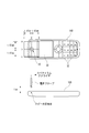
- reference numeral 16 denotes a casing of the portable terminal according to the embodiment shown in FIG. 5, and reference numeral 17 denotes a keypad.
- the key antenna 14 is designed to prevent the palm and fingertip from covering the plate-shaped inverted F antenna 11 and the inverted L antenna 14. It is desirable to be at the upper end of the terminal than the pad. The same applies to the first embodiment and the second embodiment.
- FIGS. 8A and 8B are diagrams showing an antenna device according to an embodiment of the present invention, and show an antenna device mounted on a mobile phone that can be used for GSM (registered trademark). Note that the housing is not shown in order to show the antenna device.
- a wireless communication device a mobile phone equipped with an antenna device will be described later.
- a “terminal” is an example of a wireless communication device.
- FIG. 4A shows a state where an antenna is mounted on the printed circuit board 1
- FIG. 4B is an exploded view of each component.
- the same parts as those in FIGS. 1A to 1C are denoted by the same reference numerals.
- a ground pattern (described later) is provided on the back surface of the printed circuit board 1 (on the back surface side of the drawing).
- a transmission / reception module 21 is mounted on the upper surface of the printed circuit board 1 (on the front side of the drawing).
- “mounting” refers to being directly or indirectly electrically connected to the ground pattern through a through-hole or pattern of the printed circuit board, and so on.
- the transceiver module 21 includes a transceiver circuit (not shown).
- the transmission / reception circuit includes a high-frequency signal generator circuit, a modulation circuit, a demodulation circuit, a transmission signal amplification circuit, and a reception filter circuit as main circuits.
- a power distributor 22, a band rejection filter 23, and a phase shifter 24 are mounted on the top surface of the printed circuit board 1.
- the power distributor 22 is configured by a T branch circuit.
- Various filters can be applied to the band rejection filter 23, but here, it is configured by a parallel resonance circuit of a coil and a capacitor.
- the configuration is not limited to a parallel resonance circuit of a coil and a capacitor, but a trap type SAW filter can also be employed.
- the phase shifter 24 sets a phase difference between ground currents (ground currents) input and output to and from the two antennas to a predetermined angle.
- the power distributor 22, the band rejection filter 23, and the phase shifter 24 are connected to the transmission / reception module 21 and the ground pattern via the microstrip lines 25, 26, and 27, respectively.
- Speaker 10 is mounted on the back side of printed circuit board 1.
- the back side of the printed circuit board 1 is an operation surface provided with a speaker 10 and a keypad (not shown). Therefore, the head of the user who uses the mobile phone faces the back side of the printed circuit board 1.
- the plate-like inverted F-type antenna 11 On the back surface of the printed circuit board 1 on which the transmission / reception module 21, the power distributor 22, and the band rejection filter 23 are mounted, the plate-like inverted F-type antenna 11 corresponding to the first antenna and the second antenna are also supported.
- the inverted F-type antenna 18 is mounted.
- the plate-like inverted F-type antenna 11 operates at two frequencies, frequency fl and frequency fh.
- the frequency fl is, for example, 900 MHz
- the frequency fh is, for example, 1800 MHz.
- the inverted F-type antenna 18 operates at a frequency fh (for example, 1800 MHz).
- the frequency is not limited to 900 MHz and 1800 MHz, which can be used for GSM (registered trademark) (Global System for Mobile Communications), and may be an 800 MHz band or a 1.9 GHz band. Therefore, it can also be applied to mobile phones such as LTE (Long Term Evolution) and 3G (third generation).
- the plate-like inverted F-type antenna 11 has a shape in which the radiating element is bent on the printed circuit board 1. However, if the space in the cellular phone has a margin, it is not necessarily bent.
- the printed circuit board 1 A monopole antenna may be formed on the extended surface.
- the plate-like inverted F-shaped antenna 11 has a “stapler blade” shape, and is provided with a grounding portion 12 and a power feeding portion 13 from a portion bent in an L shape.
- the ground unit 12 is a ground terminal.
- the power supply unit 13 is specifically a power supply terminal.
- the shape is not limited to this shape as long as it is an inverted F shape, and may be a U shape, an L shape, or an I shape.
- the grounding unit 12 is connected to the ground pattern, and the power feeding unit 13 is connected to the microstrip line 25.
- FIG. 9 is a rear view of the printed circuit board 1.
- the ground pattern 28 is provided on the back surface of the printed circuit board 1. Although the example in which the ground pattern 28 is provided on the substrate surface has been shown, the ground pattern 28 may be formed on the inner layer of the printed circuit board 1.
- the printed board 1 may constitute a multilayer board, and any layer may be a ground pattern.
- the ground pattern 28 may constitute a plurality of layers.
- FIGS. 10A and 10B are schematic views of the ground pattern 28 through which the ground plane current flows.
- a ground plane current flows on the ground pattern 28 shown in FIGS. 10 (a) and 10 (b).
- a ground plane current ie10 corresponding to the antenna current of the plate-like inverted F-type antenna 11 flows through the ground pattern 28 as shown in FIG.
- the ground plane current ie10 is input from the ground pattern 28 to the plate-like inverted F-type antenna 11 via the grounding portion 12, or is output from the plate-like inverted F-type antenna 11 to the ground pattern 28 via the grounding portion 12. , Current.
- the ground plane current ie20 corresponding to the antenna current of the inverted F-type antenna 18 flows through the ground pattern 28 as shown in FIG.
- the ground plane current ie20 is a current that is input from the ground pattern 28 to the inverted F-type antenna 18 via the ground unit 20 or output from the inverted F-type antenna 18 to the ground pattern 28 via the ground unit 20. .
- the phase shifter 24 controls the phase difference between the ground plane currents ie10 and ie20 so that the ground plane currents ie10 and ee20 have components that cancel each other. Specifically, the phase shifter 24 sets the phase difference between the ground plane current ie10 and the ground plane current ie20 to 180 degrees so that the ground plane current ie10 and the ground plane current ie20 flow on or near the speaker 10. ing. Note that “on the speaker” refers to a position overlapping the speaker 10 when viewed from above in FIG. 10 (a) and FIG. 10 (b). That is, as shown in FIGS.
- the ground plane currents ie10 and ie20 flow in a substantially reverse direction on the speaker 10 or in the vicinity of the speaker 10. Further, the power distributor 22 is set so that the ground plane current ie10 and the ground plane current ie20 flowing in the vicinity of the speaker 10 have the same amplitude by adjusting the distribution ratio of the transmission power from the transmission / reception circuit 4.
- the SAR can be reduced, and even when the user uses a hearing aid, the electromagnetic field intensity near the speaker 10 is reduced, so that the electromagnetic interference to the hearing aid can be reduced.
- phase shifter 24 sets the phase difference between the ground plane current ie10 and the ground plane current ie20 to 180 degrees. Since it exists, the effect of this invention can be show
- ground plane current ie10 and the ground plane current ie20 are set to the same amplitude is shown as the transmission power distribution ratio, it is not necessary to be completely the same. An optimum distribution ratio may be set according to the phase difference.
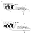
- FIGS. 12A and 12B show the measurement of power distribution in the vicinity of the speaker 10 of the GSM (registered trademark) mobile phone 100 in which the antenna device shown in FIGS. 8A and 8B is mounted inside the housing. It is a result.
- a display 33, a keypad 32, and a speaker 10 are provided on the operation surface side of the housing.
- FIG. 11 shows the measurement system.
- the speaker 10 and the coordinates that are separated from each other by ⁇ 1.67 cm in the vertical and horizontal directions with respect to the speaker 10 are indicated by using symbols a, b, c, 1, 2, and 3.
- the coordinates of the speaker 10 are (b, 2).
- the direction of a ⁇ b ⁇ c and the direction of 1 ⁇ 2 ⁇ 3 are orthogonal to each other.
- the GSM (registered trademark) mobile phone 100 receives an electric field at a point 1 cm away from the surface of the GSM (registered trademark) mobile phone 100 with an electric field probe, and measures the level with a spectrum analyzer.
- the GSM (registered trademark) mobile phone 100 is set in a state in which a telephone call is made to the base station simulator.
- the spectrum analyzer used is R3671 from ADVANTEST, and the resolution bandwidth (RBW) and video bandwidth (VBW) are set to 1 MHz.
- the electric field probe uses a coaxial cable (semi-rigid cable) processed, and the shape of the tip is connected to a conductor that extends 3 mm in each of the xyz triaxial directions after the center conductor protrudes about 2 mm. It has a different shape. This is for picking up electric field components in the triaxial direction.
- the graph (average value) in Table 1 and FIG. 12A is a measurement result of the GSM (registered trademark) mobile phone 100 in which only the plate-like inverted F-type antenna 11 is mounted.
- the graph (average value) of FIG. 12B is the measurement result of the GSM (registered trademark) mobile phone 100 in which both the plate-like inverted F-type antenna 11 and the inverted F-type antenna 18 are mounted.
- Tables 1 and 2 show the power level (dBm) at each coordinate, and details are as follows. Note that the average value of the power level at each coordinate in the case of Table 1 is ⁇ 18.6 dBm, and the average value of the power level at each coordinate in the case of Table 2 is ⁇ 20.4 dBm.
- the level (power level) of the speaker 10 and the average level in the vicinity including the speaker 10 are lowered. It can be seen that the electromagnetic field strength in the vicinity can be reduced.
- the example of the mobile phone has been described, as a wireless communication device to which the present invention can be applied, it is also possible to apply to a cordless phone slave unit and a tablet terminal.
- the first antenna device in the present embodiment is an antenna device having a plurality of antennas, and includes a first antenna having a first ground terminal, a second antenna having a second ground terminal, One antenna is connected via the first ground terminal, the second antenna is connected via the second ground terminal, and the first conductor is connected to the first ground terminal via the first ground terminal.
- phase shifter that controls a phase difference between the second current output from the second antenna to the ground conductor via the second ground terminal, and the phase shifter includes: The current and the second current To have a destructive component, to control the phase difference between the first and second currents.
- the electromagnetic field intensity accompanying the current flowing in the first antenna and the second antenna can be efficiently reduced.
- the second antenna device further includes a printed circuit board having a first surface and a second surface that is the back side of the first surface, and the first antenna and the second antenna are the first antenna and the second antenna.
- the ground conductor is provided on the second surface.
- the ground conductor in which the first current and the second current are canceled is provided on the surface where the first antenna and the second antenna are not provided, the space for the ground conductor can be increased. Current and the second current can be effectively canceled out.
- the ground conductor is a ground pattern that covers the second surface.
- the ground conductor can be formed on the entire second surface as a ground pattern, the first current and the second current can be canceled out more efficiently.
- the phase shifter controls the phase difference between the first current and the second current to be approximately 180 degrees.
- the component that cancels the first current and the second current can be made as large as possible, the electromagnetic field intensity associated with the current flowing through the first antenna and the second antenna can be more efficiently reduced. can do.
- the fifth antenna device further includes a power distributor that distributes the power of the current flowing through the first antenna and the power of the current flowing through the second antenna substantially equally.
- the component that cancels the first current and the second current can be made as large as possible, the electromagnetic field intensity associated with the current flowing through the first antenna and the second antenna can be more efficiently reduced. can do.
- the first antenna uses the first frequency corresponding to the first current
- the second antenna corresponds to the second current
- the first frequency is used.
- the first current and the second current flow at the same frequency, the first current and the second current can be efficiently canceled out.
- the seventh antenna device in the present embodiment is a wireless communication device that performs wireless communication, an antenna device having a plurality of antennas, a first antenna having a first ground terminal, and a second antenna device.
- a second antenna having a ground terminal, a ground conductor connected to the first antenna via the first ground terminal, and a second conductor connected to the second antenna via the second ground terminal;
- To the first antenna through the first ground terminal, or from the first antenna to the ground conductor through the first ground terminal, and from the ground conductor to the second A phase shifter that controls a phase difference between the second current that is input to the second antenna via the ground terminal or that is output from the second antenna to the ground conductor via the second ground terminal; , Output audio And a phase shifter between the first current and the second current so that the first current and the second current cancel each other on or near the speaker. Control the phase difference.
- the component that cancels the first current and the second current can be made as large as possible, the electromagnetic field intensity associated with the current flowing through the first antenna and the second antenna can be more efficiently reduced. can do. Therefore, the influence of the electromagnetic field intensity on the speaker can be suppressed.
- the present invention is useful for an antenna device, a wireless communication device, and the like mounted on a portable wireless terminal such as a cellular phone that can reduce the electromagnetic field intensity near the human head.
Landscapes
- Engineering & Computer Science (AREA)
- Computer Networks & Wireless Communication (AREA)
- Signal Processing (AREA)
- Support Of Aerials (AREA)
- Variable-Direction Aerials And Aerial Arrays (AREA)
- Details Of Aerials (AREA)
- Telephone Set Structure (AREA)
Abstract
Description
(実施の形態1)
図3(a),(b)は、本発明の1実施の形態に係るアンテナ装置を示す図である。図1(a)~(c)と同一部品には同一番号を付している。図3(a)において符号1は端末機本体のプリント基板、符号2はプリント基板1の左端に設けた第1の逆L型アンテナであり、符号3はプリント基板左端において、給電点から放射素子の伸びる方向が、第1の逆L型アンテナと対向するように設けられ、第1の逆L型アンテナ2と同一周波数で動作する第2の逆L型アンテナである。図3(b)は図3(a)の側面図である。
図5(a),(b),(c)は、本発明の1実施の形態に係るアンテナ装置を示す図である。図1(a)~(c)と同一部品には同一番号を付している。
図8(a),(b)は、本発明の1実施の形態に係るアンテナ装置を示す図であり、GSM(登録商標)に利用可能な携帯電話に搭載されたアンテナ装置を示している。なお、アンテナ装置を示すため、筐体は図示していない。無線通信装置の一例として、アンテナ装置を実装した携帯電話については後述する。なお、「端末機」は無線通信装置の一例である。


本出願は、2011年1月26日出願の日本特許出願No.2011-013622に基づくものであり、その内容はここに参照として取り込まれる。
2 逆L型アンテナ
3 逆L型アンテナ
4 送受信回路
5 電力分配器
6 マイクロストリップ線路
7 位相器
8 マイクロストリップ線路
9 マイクロストリップ線路
10 スピーカ
11 板状逆F型アンテナ
12 板状逆F型アンテナの接地部
13 板状逆F型アンテナの給電部
14 逆L型アンテナ
15 帯域阻止フィルタ
16 筐体
17 キーパッド
18 逆F型アンテナ
19 逆F型アンテナの給電部
20 逆F型アンテナの接地部
21 送受信モジュール
22 電力分配器
23 帯域阻止フィルタ
24 位相器
25 マイクロストリップ線路
26 マイクロストリップ線路
27 マイクロストリップ線路
28 グランドパターン
100 GSM(登録商標)携帯電話
Claims (7)
- 複数のアンテナを有するアンテナ装置であって、
第1の接地端子を有する第1のアンテナと、
第2の接地端子を有する第2のアンテナと、
前記第1のアンテナが前記第1の接地端子を介して接続され、前記第2のアンテナが前記第2の接地端子を介して接続されたグランド導体と、
前記グランド導体から前記第1の接地端子を介して前記第1のアンテナに入力される、または前記第1のアンテナから前記第1の接地端子を介して前記グランド導体に出力される第1の電流と、前記グランド導体から前記第2の接地端子を介して前記第2のアンテナに入力される、または前記第2アンテナから前記第2の接地端子を介して前記グランド導体に出力される第2の電流と、の間の位相差を制御する位相器と、
を備え、
前記位相器は、前記第1の電流および前記第2の電流が互いに打ち消しあう成分を有するように、前記第1の電流および前記第2の電流間の位相差を制御するアンテナ装置。 - 更に、第1の面と、前記第1の面の裏側である第2の面と、有するプリント基板を備え、
前記第1のアンテナおよび前記第2のアンテナは前記第1の面に設けられ、
前記グランド導体は前記第2の面に設けられている、
請求項1記載のアンテナ装置。 - 前記グランド導体は、前記第2の面を覆うグランドパターンである、
請求項2記載のアンテナ装置。 - 前記位相器は、前記第1の電流および前記第2の電流間の位相差を、略180度になるように制御する、
請求項1ないし3いずれか1項に記載のアンテナ装置。 - 更に、前記第1のアンテナを流れる電流の電力と、前記第2のアンテナを流れる電流の電力と、を略等しく分配する電力分配器を備える、
請求項1ないし4いずれか1項に記載のアンテナ装置。 - 前記第1のアンテナは、前記第1の電流に対応する第1の周波数を用い、
前記第2のアンテナは、前記第2の電流に対応しかつ前記第1の周波数と同一の第2の周波数を用いる、
請求項1ないし4いずれか1項に記載のアンテナ装置。 - 無線で通信を行う無線通信装置であって、
複数のアンテナを有するアンテナ装置であって、
第1の接地端子を有する第1のアンテナと、
第2の接地端子を有する第2のアンテナと、
前記第1のアンテナが前記第1の接地端子を介して接続され、前記第2のアンテナが前記第2の接地端子を介して接続されたグランド導体と、
前記グランド導体から前記第1の接地端子を介して前記第1のアンテナに入力される、または前記第1のアンテナから前記第1の接地端子を介して前記グランド導体に出力される第1の電流と、前記グランド導体から前記第2の接地端子を介して前記第2のアンテナに入力される、または前記第2アンテナから前記第2の接地端子を介して前記グランド導体に出力される第2の電流と、の間の位相差を制御する位相器と、
音声を出力するスピーカと、
を備え、
前記位相器は、前記スピーカ上またはスピーカ近傍において、前記第1の電流および前記第2の電流が互いに打ち消しあう成分を有するように、前記第1の電流および前記第2の電流間の位相差を制御する無線通信装置。
Priority Applications (2)
| Application Number | Priority Date | Filing Date | Title |
|---|---|---|---|
| US13/981,906 US9184509B2 (en) | 2011-01-26 | 2012-01-26 | Antenna device and wireless communication apparatus |
| JP2012553126A JP5288668B2 (ja) | 2011-01-26 | 2012-01-26 | アンテナ装置および無線通信装置 |
Applications Claiming Priority (2)
| Application Number | Priority Date | Filing Date | Title |
|---|---|---|---|
| JP2011-013622 | 2011-01-26 | ||
| JP2011013622 | 2011-01-26 |
Publications (1)
| Publication Number | Publication Date |
|---|---|
| WO2012102047A1 true WO2012102047A1 (ja) | 2012-08-02 |
Family
ID=46580622
Family Applications (1)
| Application Number | Title | Priority Date | Filing Date |
|---|---|---|---|
| PCT/JP2012/000499 Ceased WO2012102047A1 (ja) | 2011-01-26 | 2012-01-26 | アンテナ装置および無線通信装置 |
Country Status (3)
| Country | Link |
|---|---|
| US (1) | US9184509B2 (ja) |
| JP (1) | JP5288668B2 (ja) |
| WO (1) | WO2012102047A1 (ja) |
Families Citing this family (8)
| Publication number | Priority date | Publication date | Assignee | Title |
|---|---|---|---|---|
| CN104599431B (zh) | 2004-11-12 | 2018-03-27 | 爱克斯崔里斯科技有限公司 | 微粒探测器,系统与方法 |
| KR20160019437A (ko) * | 2013-06-14 | 2016-02-19 | 르네사스 일렉트로닉스 가부시키가이샤 | 통신 제어 장치 및 실장 기판 |
| CN104157976A (zh) * | 2014-07-29 | 2014-11-19 | 深圳市中兴物联科技有限公司 | 天线装置和通信终端 |
| US10051388B2 (en) | 2016-09-21 | 2018-08-14 | Starkey Laboratories, Inc. | Radio frequency antenna for an in-the-ear hearing device |
| JP2020036187A (ja) * | 2018-08-30 | 2020-03-05 | レノボ・シンガポール・プライベート・リミテッド | アンテナ装置及び電子機器 |
| WO2022098172A1 (ko) | 2020-11-06 | 2022-05-12 | 삼성전자 주식회사 | 신호 보정을 위한 안테나 구조 및 방법 |
| CN115426424B (zh) * | 2022-08-31 | 2024-12-17 | 维沃移动通信有限公司 | 电子设备 |
| CN119542741B (zh) * | 2023-08-28 | 2025-10-17 | Oppo广东移动通信有限公司 | 电子设备 |
Citations (3)
| Publication number | Priority date | Publication date | Assignee | Title |
|---|---|---|---|---|
| JP2002152115A (ja) * | 2000-11-13 | 2002-05-24 | Samsung Yokohama Research Institute Co Ltd | 携帯端末機 |
| JP2006050324A (ja) * | 2004-08-05 | 2006-02-16 | Matsushita Electric Ind Co Ltd | 携帯無線機 |
| JP2008072486A (ja) * | 2006-09-14 | 2008-03-27 | Sharp Corp | 携帯無線機用アンテナ及び携帯無線機 |
Family Cites Families (4)
| Publication number | Priority date | Publication date | Assignee | Title |
|---|---|---|---|---|
| JP2001119238A (ja) * | 1999-10-18 | 2001-04-27 | Sony Corp | アンテナ装置及び携帯無線機 |
| KR100446506B1 (ko) | 2000-11-13 | 2004-09-04 | 삼성전자주식회사 | 휴대 단말기 |
| JPWO2007029741A1 (ja) * | 2005-09-09 | 2009-03-19 | パナソニック株式会社 | 無線機用アンテナ装置及び携帯無線機 |
| JP2010187336A (ja) | 2009-02-13 | 2010-08-26 | Furukawa Electric Co Ltd:The | 車載用複合アンテナ |
-
2012
- 2012-01-26 WO PCT/JP2012/000499 patent/WO2012102047A1/ja not_active Ceased
- 2012-01-26 JP JP2012553126A patent/JP5288668B2/ja not_active Expired - Fee Related
- 2012-01-26 US US13/981,906 patent/US9184509B2/en not_active Expired - Fee Related
Patent Citations (3)
| Publication number | Priority date | Publication date | Assignee | Title |
|---|---|---|---|---|
| JP2002152115A (ja) * | 2000-11-13 | 2002-05-24 | Samsung Yokohama Research Institute Co Ltd | 携帯端末機 |
| JP2006050324A (ja) * | 2004-08-05 | 2006-02-16 | Matsushita Electric Ind Co Ltd | 携帯無線機 |
| JP2008072486A (ja) * | 2006-09-14 | 2008-03-27 | Sharp Corp | 携帯無線機用アンテナ及び携帯無線機 |
Also Published As
| Publication number | Publication date |
|---|---|
| JPWO2012102047A1 (ja) | 2014-06-30 |
| US20140152515A9 (en) | 2014-06-05 |
| JP5288668B2 (ja) | 2013-09-11 |
| US9184509B2 (en) | 2015-11-10 |
| US20130307738A1 (en) | 2013-11-21 |
Similar Documents
| Publication | Publication Date | Title |
|---|---|---|
| JP5288668B2 (ja) | アンテナ装置および無線通信装置 | |
| US7911405B2 (en) | Multi-band low profile antenna with low band differential mode | |
| JP4132669B2 (ja) | 無給電放射素子を有するデュアル・バンド・ダイバーシチ・アンテナ | |
| US8044863B2 (en) | Low profile, folded antenna assembly for handheld communication devices | |
| CN102804487B (zh) | 包括环状天线的用于无线通信的装置 | |
| US11355853B2 (en) | Antenna structure and wireless communication device using the same | |
| CN102157778B (zh) | 实现sar控制的方法和装置 | |
| CN105609969A (zh) | 通信终端 | |
| KR20020027636A (ko) | 안테나 장치 및 휴대용 무선 통신 장치 | |
| KR20140119928A (ko) | 전도성 테두리를 이용한 다중 대역 안테나를 포함하는 단말기 | |
| KR20070122101A (ko) | 휴대 단말기 | |
| WO2021203939A1 (zh) | 一种电子设备 | |
| JP6687243B2 (ja) | 無線通信装置 | |
| CN205509020U (zh) | 通信终端 | |
| CN106033842A (zh) | 天线及电子设备 | |
| CN104466357A (zh) | 一种天线装置及终端 | |
| US9450287B2 (en) | Broadband antenna and wireless communication device employing same | |
| JP2002152353A (ja) | 携帯端末機 | |
| CN102420884A (zh) | 天线布置改良的金属面壳移动终端 | |
| WO2017113270A1 (zh) | 天线装置和终端 | |
| TWI508375B (zh) | 天線模組 | |
| US20060139214A1 (en) | Antenna | |
| TWI571002B (zh) | 天線裝置及應用其之通訊裝置 | |
| CN202585708U (zh) | 天线布置改良的金属面壳移动终端 | |
| CN211126056U (zh) | 一种天线组件及电子设备 |
Legal Events
| Date | Code | Title | Description |
|---|---|---|---|
| 121 | Ep: the epo has been informed by wipo that ep was designated in this application |
Ref document number: 12739852 Country of ref document: EP Kind code of ref document: A1 |
|
| WWE | Wipo information: entry into national phase |
Ref document number: 2012553126 Country of ref document: JP |
|
| WWE | Wipo information: entry into national phase |
Ref document number: 13981906 Country of ref document: US |
|
| NENP | Non-entry into the national phase |
Ref country code: DE |
|
| 122 | Ep: pct application non-entry in european phase |
Ref document number: 12739852 Country of ref document: EP Kind code of ref document: A1 |