WO2012102152A1 - 貼り合わせ用パネル、表示ユニット及び表示装置 - Google Patents
貼り合わせ用パネル、表示ユニット及び表示装置 Download PDFInfo
- Publication number
- WO2012102152A1 WO2012102152A1 PCT/JP2012/050988 JP2012050988W WO2012102152A1 WO 2012102152 A1 WO2012102152 A1 WO 2012102152A1 JP 2012050988 W JP2012050988 W JP 2012050988W WO 2012102152 A1 WO2012102152 A1 WO 2012102152A1
- Authority
- WO
- WIPO (PCT)
- Prior art keywords
- edge
- panel
- substrate
- display unit
- display
- Prior art date
- Legal status (The legal status is an assumption and is not a legal conclusion. Google has not performed a legal analysis and makes no representation as to the accuracy of the status listed.)
- Ceased
Links
Images











Classifications
-
- G—PHYSICS
- G02—OPTICS
- G02F—OPTICAL DEVICES OR ARRANGEMENTS FOR THE CONTROL OF LIGHT BY MODIFICATION OF THE OPTICAL PROPERTIES OF THE MEDIA OF THE ELEMENTS INVOLVED THEREIN; NON-LINEAR OPTICS; FREQUENCY-CHANGING OF LIGHT; OPTICAL LOGIC ELEMENTS; OPTICAL ANALOGUE/DIGITAL CONVERTERS
- G02F1/00—Devices or arrangements for the control of the intensity, colour, phase, polarisation or direction of light arriving from an independent light source, e.g. switching, gating or modulating; Non-linear optics
- G02F1/01—Devices or arrangements for the control of the intensity, colour, phase, polarisation or direction of light arriving from an independent light source, e.g. switching, gating or modulating; Non-linear optics for the control of the intensity, phase, polarisation or colour
- G02F1/13—Devices or arrangements for the control of the intensity, colour, phase, polarisation or direction of light arriving from an independent light source, e.g. switching, gating or modulating; Non-linear optics for the control of the intensity, phase, polarisation or colour based on liquid crystals, e.g. single liquid crystal display cells
- G02F1/133—Constructional arrangements; Operation of liquid crystal cells; Circuit arrangements
- G02F1/1333—Constructional arrangements; Manufacturing methods
-
- G—PHYSICS
- G06—COMPUTING OR CALCULATING; COUNTING
- G06F—ELECTRIC DIGITAL DATA PROCESSING
- G06F3/00—Input arrangements for transferring data to be processed into a form capable of being handled by the computer; Output arrangements for transferring data from processing unit to output unit, e.g. interface arrangements
- G06F3/01—Input arrangements or combined input and output arrangements for interaction between user and computer
- G06F3/03—Arrangements for converting the position or the displacement of a member into a coded form
- G06F3/041—Digitisers, e.g. for touch screens or touch pads, characterised by the transducing means
-
- B—PERFORMING OPERATIONS; TRANSPORTING
- B32—LAYERED PRODUCTS
- B32B—LAYERED PRODUCTS, i.e. PRODUCTS BUILT-UP OF STRATA OF FLAT OR NON-FLAT, e.g. CELLULAR OR HONEYCOMB, FORM
- B32B2457/00—Electrical equipment
- B32B2457/20—Displays, e.g. liquid crystal displays, plasma displays
-
- B—PERFORMING OPERATIONS; TRANSPORTING
- B32—LAYERED PRODUCTS
- B32B—LAYERED PRODUCTS, i.e. PRODUCTS BUILT-UP OF STRATA OF FLAT OR NON-FLAT, e.g. CELLULAR OR HONEYCOMB, FORM
- B32B37/00—Methods or apparatus for laminating, e.g. by curing or by ultrasonic bonding
- B32B37/12—Methods or apparatus for laminating, e.g. by curing or by ultrasonic bonding characterised by using adhesives
-
- G—PHYSICS
- G02—OPTICS
- G02F—OPTICAL DEVICES OR ARRANGEMENTS FOR THE CONTROL OF LIGHT BY MODIFICATION OF THE OPTICAL PROPERTIES OF THE MEDIA OF THE ELEMENTS INVOLVED THEREIN; NON-LINEAR OPTICS; FREQUENCY-CHANGING OF LIGHT; OPTICAL LOGIC ELEMENTS; OPTICAL ANALOGUE/DIGITAL CONVERTERS
- G02F1/00—Devices or arrangements for the control of the intensity, colour, phase, polarisation or direction of light arriving from an independent light source, e.g. switching, gating or modulating; Non-linear optics
- G02F1/01—Devices or arrangements for the control of the intensity, colour, phase, polarisation or direction of light arriving from an independent light source, e.g. switching, gating or modulating; Non-linear optics for the control of the intensity, phase, polarisation or colour
- G02F1/13—Devices or arrangements for the control of the intensity, colour, phase, polarisation or direction of light arriving from an independent light source, e.g. switching, gating or modulating; Non-linear optics for the control of the intensity, phase, polarisation or colour based on liquid crystals, e.g. single liquid crystal display cells
- G02F1/133—Constructional arrangements; Operation of liquid crystal cells; Circuit arrangements
- G02F1/1333—Constructional arrangements; Manufacturing methods
- G02F1/133351—Manufacturing of individual cells out of a plurality of cells, e.g. by dicing
-
- G—PHYSICS
- G02—OPTICS
- G02F—OPTICAL DEVICES OR ARRANGEMENTS FOR THE CONTROL OF LIGHT BY MODIFICATION OF THE OPTICAL PROPERTIES OF THE MEDIA OF THE ELEMENTS INVOLVED THEREIN; NON-LINEAR OPTICS; FREQUENCY-CHANGING OF LIGHT; OPTICAL LOGIC ELEMENTS; OPTICAL ANALOGUE/DIGITAL CONVERTERS
- G02F1/00—Devices or arrangements for the control of the intensity, colour, phase, polarisation or direction of light arriving from an independent light source, e.g. switching, gating or modulating; Non-linear optics
- G02F1/01—Devices or arrangements for the control of the intensity, colour, phase, polarisation or direction of light arriving from an independent light source, e.g. switching, gating or modulating; Non-linear optics for the control of the intensity, phase, polarisation or colour
- G02F1/13—Devices or arrangements for the control of the intensity, colour, phase, polarisation or direction of light arriving from an independent light source, e.g. switching, gating or modulating; Non-linear optics for the control of the intensity, phase, polarisation or colour based on liquid crystals, e.g. single liquid crystal display cells
- G02F1/133—Constructional arrangements; Operation of liquid crystal cells; Circuit arrangements
- G02F1/1333—Constructional arrangements; Manufacturing methods
- G02F1/133368—Cells having two substrates with different characteristics, e.g. different thickness or material
-
- G—PHYSICS
- G02—OPTICS
- G02F—OPTICAL DEVICES OR ARRANGEMENTS FOR THE CONTROL OF LIGHT BY MODIFICATION OF THE OPTICAL PROPERTIES OF THE MEDIA OF THE ELEMENTS INVOLVED THEREIN; NON-LINEAR OPTICS; FREQUENCY-CHANGING OF LIGHT; OPTICAL LOGIC ELEMENTS; OPTICAL ANALOGUE/DIGITAL CONVERTERS
- G02F1/00—Devices or arrangements for the control of the intensity, colour, phase, polarisation or direction of light arriving from an independent light source, e.g. switching, gating or modulating; Non-linear optics
- G02F1/01—Devices or arrangements for the control of the intensity, colour, phase, polarisation or direction of light arriving from an independent light source, e.g. switching, gating or modulating; Non-linear optics for the control of the intensity, phase, polarisation or colour
- G02F1/13—Devices or arrangements for the control of the intensity, colour, phase, polarisation or direction of light arriving from an independent light source, e.g. switching, gating or modulating; Non-linear optics for the control of the intensity, phase, polarisation or colour based on liquid crystals, e.g. single liquid crystal display cells
- G02F1/133—Constructional arrangements; Operation of liquid crystal cells; Circuit arrangements
- G02F1/1333—Constructional arrangements; Manufacturing methods
- G02F1/13338—Input devices, e.g. touch panels
-
- G—PHYSICS
- G02—OPTICS
- G02F—OPTICAL DEVICES OR ARRANGEMENTS FOR THE CONTROL OF LIGHT BY MODIFICATION OF THE OPTICAL PROPERTIES OF THE MEDIA OF THE ELEMENTS INVOLVED THEREIN; NON-LINEAR OPTICS; FREQUENCY-CHANGING OF LIGHT; OPTICAL LOGIC ELEMENTS; OPTICAL ANALOGUE/DIGITAL CONVERTERS
- G02F1/00—Devices or arrangements for the control of the intensity, colour, phase, polarisation or direction of light arriving from an independent light source, e.g. switching, gating or modulating; Non-linear optics
- G02F1/01—Devices or arrangements for the control of the intensity, colour, phase, polarisation or direction of light arriving from an independent light source, e.g. switching, gating or modulating; Non-linear optics for the control of the intensity, phase, polarisation or colour
- G02F1/13—Devices or arrangements for the control of the intensity, colour, phase, polarisation or direction of light arriving from an independent light source, e.g. switching, gating or modulating; Non-linear optics for the control of the intensity, phase, polarisation or colour based on liquid crystals, e.g. single liquid crystal display cells
- G02F1/133—Constructional arrangements; Operation of liquid crystal cells; Circuit arrangements
- G02F1/1333—Constructional arrangements; Manufacturing methods
- G02F1/1347—Arrangement of liquid crystal layers or cells in which the final condition of one light beam is achieved by the addition of the effects of two or more layers or cells
-
- G—PHYSICS
- G02—OPTICS
- G02F—OPTICAL DEVICES OR ARRANGEMENTS FOR THE CONTROL OF LIGHT BY MODIFICATION OF THE OPTICAL PROPERTIES OF THE MEDIA OF THE ELEMENTS INVOLVED THEREIN; NON-LINEAR OPTICS; FREQUENCY-CHANGING OF LIGHT; OPTICAL LOGIC ELEMENTS; OPTICAL ANALOGUE/DIGITAL CONVERTERS
- G02F2201/00—Constructional arrangements not provided for in groups G02F1/00 - G02F7/00
- G02F2201/12—Constructional arrangements not provided for in groups G02F1/00 - G02F7/00 electrode
- G02F2201/124—Constructional arrangements not provided for in groups G02F1/00 - G02F7/00 electrode interdigital
-
- G—PHYSICS
- G02—OPTICS
- G02F—OPTICAL DEVICES OR ARRANGEMENTS FOR THE CONTROL OF LIGHT BY MODIFICATION OF THE OPTICAL PROPERTIES OF THE MEDIA OF THE ELEMENTS INVOLVED THEREIN; NON-LINEAR OPTICS; FREQUENCY-CHANGING OF LIGHT; OPTICAL LOGIC ELEMENTS; OPTICAL ANALOGUE/DIGITAL CONVERTERS
- G02F2201/00—Constructional arrangements not provided for in groups G02F1/00 - G02F7/00
- G02F2201/50—Protective arrangements
- G02F2201/503—Arrangements improving the resistance to shock
-
- G—PHYSICS
- G02—OPTICS
- G02F—OPTICAL DEVICES OR ARRANGEMENTS FOR THE CONTROL OF LIGHT BY MODIFICATION OF THE OPTICAL PROPERTIES OF THE MEDIA OF THE ELEMENTS INVOLVED THEREIN; NON-LINEAR OPTICS; FREQUENCY-CHANGING OF LIGHT; OPTICAL LOGIC ELEMENTS; OPTICAL ANALOGUE/DIGITAL CONVERTERS
- G02F2202/00—Materials and properties
- G02F2202/28—Adhesive materials or arrangements
-
- G—PHYSICS
- G06—COMPUTING OR CALCULATING; COUNTING
- G06F—ELECTRIC DIGITAL DATA PROCESSING
- G06F2203/00—Indexing scheme relating to G06F3/00 - G06F3/048
- G06F2203/041—Indexing scheme relating to G06F3/041 - G06F3/045
- G06F2203/04103—Manufacturing, i.e. details related to manufacturing processes specially suited for touch sensitive devices
Definitions
- the present invention relates to a bonding panel, a display unit, and a display device for bonding to a target panel with an adhesive.
- a display device that not only displays a flat image but also implements various functions by arranging a functional panel on the surface of the display panel.
- a functional panel having a parallax barrier function on the surface of the display panel, a function of switching and displaying a 2D (planar) image and a 3D (stereoscopic) image is realized, or a single display screen is used.
- a dual view display function for displaying different images depending on the viewing direction.
- Such a functional panel is generally attached to the surface of the display panel with an adhesive.
- the display apparatus which has a functional panel is comprised.
- the adhesive may protrude from between the display panel and the functional panel. If this adhesive protrudes too much, the outer shape becomes large, and when a display panel to which a functional panel is attached is incorporated into a module or product, cracks or misalignment may occur.
- Patent Document 1 discloses a display device capable of dual view display by attaching a parallax barrier substrate to a liquid crystal display panel via an adhesive.
- FIG. 20 is a cross-sectional view showing the configuration of the display device of Patent Document 1.
- the liquid crystal display device 500 includes a liquid crystal display panel 510 that performs image display, and a parallax barrier substrate 520 disposed on the front side of the liquid crystal display panel 510 with an adhesive resin layer 518 interposed therebetween. .
- the parallax barrier substrate 520 includes a glass substrate 521 and a transmission control unit 522 that controls an image that can be viewed according to the viewing directions Z1 and Z2.
- the transmission control unit 522 has a plurality of translucent slits provided so as to extend linearly in parallel to each other, and a light shielding unit provided between the translucent slits.
- the parallax barrier substrate 520 is formed with a notch 520 a that is partly cut out in the thickness direction on the liquid crystal display panel 510 side of the peripheral portion disposed so as to overlap the liquid crystal display panel 510.
- the notch 520 a is configured by the inclined side surface of the parallax barrier substrate 520 and is formed over the entire periphery of the peripheral edge of the parallax barrier substrate 520.
- the notch 520a is formed by chamfering the glass substrate 521 by polishing, etching, or the like.
- the liquid crystal display device 500 is provided with the notch 520a at the peripheral edge of the parallax barrier substrate 520.
- the adhesive resin material that becomes the adhesive resin layer 518 pushed out between the liquid crystal display panel 510 and the parallax barrier substrate 520 is converted into the parallax barrier. It enters into the notch of the substrate 520. For this reason, the adhesive resin layer 518 obtained by curing the adhesive resin material can be prevented from protruding from between the liquid crystal display panel 510 and the parallax barrier substrate 520.
- the parallax barrier substrate 520 includes the single glass substrate 521 and the transmission control unit 522, the thickness is relatively thin. For this reason, even if the notch part 520a is provided in the parallax barrier substrate 520 having a relatively small thickness, the volume of the space formed between the notch part 520a and the liquid crystal display panel 510 does not increase so much.
- the effect of suppressing the protrusion of the adhesive resin layer 518 when the liquid crystal display panel 510 and the parallax barrier substrate 520 are bonded together is insufficient.
- the present invention has been made to solve the above-mentioned problems, and its purpose is to effectively prevent the occurrence of a defective outer shape.
- a bonding panel is a bonding panel that includes first and second substrates disposed opposite to each other, and is bonded to a target panel by an adhesive,
- the first substrate that is far from the first substrate includes first and second edges facing each other, and the second substrate that is closer to the target panel is a third edge located inside the first edge in plan view. And a fourth edge located inside the second edge in plan view.
- a step is formed by the first edge and the third edge, and a step is formed by the second edge and the fourth edge.
- the pressed adhesive has a step between the first edge and the third edge, and the fourth edge and the above. Since it becomes possible to enter the step with the second edge, it is possible to more effectively prevent the appearance defect.
- the laminating panel of the present invention is a laminating panel that includes first and second substrates disposed opposite to each other, and is bonded to the target panel by an adhesive, and the first substrate that is farther from the target panel is
- the second substrate including the first and second edges facing each other and closer to the target panel has a third edge located inside the first edge in plan view, and a second edge in plan view. And a fourth edge located inside thereof.
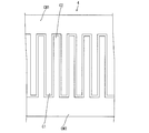
- FIG. 3 is a plan view illustrating a configuration of SEG electrodes of the SEG substrate according to Embodiment 1.
- FIG. 3 is a plan view illustrating a configuration of a COM electrode disposed on the COM substrate according to the first embodiment.
- FIG. 4 is an enlarged view of a region X in FIG. 3.
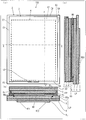
- A) is a top view showing the structure of the display unit of Embodiment 1,
- (b) is AA 'arrow sectional drawing of (a),
- (c) is B of (a).
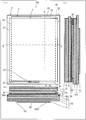
- (A) is a top view showing the structure of the display unit of the modification 1 of Embodiment 1,
- (b) is the EE 'sectional view taken on the line (a)
- (c) is (a)
- FIG. (A) is a top view showing the structure of the display unit of the modification 1 of Embodiment 1,
- (b) is the EE 'sectional view taken on the line (a)
- (c) is (a) FIG.
- FIG. (A) is a top view showing the structure of the display unit of the modification 2 of Embodiment 1, (b) is GG 'sectional view taken on the line of (a), (c) is (a).
- FIG. (A) is a top view showing the structure of the display unit of the modification 2 of Embodiment 1, (b) is GG 'sectional view taken on the line of (a), (c) is (a).
- FIG. (A) is a top view showing the structure of the display unit of the modification 3 of Embodiment 1, (b) is the II 'sectional view taken on the line of (a), (c) is (a). It is JJ 'line sectional drawing of.
- FIG. (A) is a top view showing the structure of the display unit of the modification 3 of Embodiment 1, (b) is the II 'sectional view taken on the line of (a), (c) is (a). It is JJ 'line sectional drawing of.
- (A) is a top view showing the structure of the display unit of Embodiment 2
- (b) is KK 'line sectional drawing of (a)
- (c) is LL of (a).
- FIG. (A) is a top view showing the structure of the display unit which concerns on Embodiment 2
- (b) is KK 'arrow sectional drawing of (a)
- (c) is (a). It is LL 'sectional view taken on the line.
- FIG. (A) is a top view showing the structure of the display unit of Embodiment 3, (b) is MM 'sectional view taken on the line of (a), (c) is NN of (a).
- FIG. (A) is a top view showing the structure of the display unit of Embodiment 3, (b) is MM 'sectional view taken on the line of (a), (c) is NN of (a).
- FIG. (A) is a top view showing the structure of the display unit of the modification 1 of Embodiment 3, (b) is OO 'line sectional drawing of (a), (c) is (a).
- FIG. 1 is a top view showing the structure of the display unit of the modification 1 of Embodiment 3
- (b) is OO 'line sectional drawing of (a)
- (c) is (a).
- FIG. It is sectional drawing showing the structure of the conventional display apparatus.
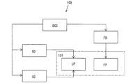
- FIG. 2 is a block diagram showing the configuration of the display device 100.
- the display device 100 includes a display unit 101, a source driver SD, a gate driver GD, a function panel driver FD, and a display control circuit DCC.
- the display unit 101 includes a display panel LP and a function panel FP.
- the display unit 101 is a display unit capable of switching between 2D (planar image) display and 3D (stereoscopic image).
- the display panel LP is a display panel for image display, for example, a liquid crystal panel.
- the function panel FP is provided with an additional function on the display panel LP by being attached to the display panel LP via an adhesive.
- the function panel FP is a parallax barrier switch panel.
- the display unit 101 can realize switching of 3D (stereoscopic) display mode to be valid or invalid.
- the 3D display mode refers to giving a specific viewing angle to each of the right-eye image and the left-eye image of the display panel LP, and allowing the observer to visually recognize only the image corresponding to each eye. In this mode, the stereoscopic image is visually recognized.
- the functional panel FP is a panel capable of forming a slit-like barrier (parallax barrier) for controlling the viewing angle.
- the display control circuit DCC is for performing overall drive control of the display device 100.
- the display control circuit DCC generates a display image signal to be displayed on the display panel LP, or a function panel.
- a signal for driving control of the FP is generated.
- the display control circuit DCC generates a source signal and a gate signal as display image signals. Then, the display control circuit DCC outputs a source signal to the source driver SD and outputs a gate signal to the gate driver GD. Accordingly, the source driver SD outputs a source signal to a plurality of source lines arranged on the active substrate of the display panel LP, and the gate driver GD outputs a plurality of gates arranged on the active substrate of the display panel LP. A gate signal is output to the wiring. Thereby, an image is displayed on the image display part of the display panel LP.
- the display control circuit DCC when the display control circuit DCC generates a signal for driving control of the function panel FP, the signal is output to the function panel driver FD.
- the function panel driver FD controls driving of the function panel FP by outputting a signal for driving control of the function panel FP to the function panel FP.
- the signal for controlling the driving of the function panel FP is a signal synchronized with an image to be displayed on the display panel LP when the display unit 101 performs 3D display.
- the source driver SD, the gate driver GD, the function panel driver FD, and the display control circuit DCC are generally used for display devices capable of switching between display of 2D images and 3D images. Things can be used.
- the source driver SD and the gate driver GD may be provided directly on the display panel LP, or may be provided on a printed board (not shown) connected to the display panel LP.
- the display device 100 may include a backlight (not shown).
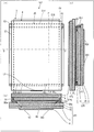
- Display unit 101 The configuration of the display unit 101 will be described with reference to (a) to (c) of FIG.
- FIG. 1A is a plan view showing the configuration of the display unit 101 according to the present embodiment
- FIG. 1B is a cross-sectional view taken along line AA ′ in FIG. 1A
- FIG. It is BB 'sectional view taken on the line of (a).
- the display unit 101 includes an adhesive BO, a function panel FP, and a display panel LP for image display.
- the functional panel FP and the display panel LP are pasted through an adhesive BO.
- the function panel FP is provided on the viewing side from the display panel LP.
- the adhesive BO is in a liquid state and is applied to one of the function panel FP or the display panel LP, and after the other is bonded, the function BO FP and the display panel LP are cured by heat or light. It is to be fixed.
- the adhesive BO is made of, for example, a general thermosetting or photocurable transparent acrylic material.
- the thickness of the adhesive BO disposed between the polarizing plate 5 disposed on the surface of the display panel LP and the functional panel FP is about 0.05 mmt.
- the display panel LP includes an active substrate 2, a counter substrate 1, and polarizing plates 5 and 6.
- the display panel LP is a liquid crystal panel in which an active substrate 2 and a counter substrate 1 are arranged to face each other via liquid crystal (not shown).
- the active substrate 2 includes a plurality of source wirings arranged on a glass substrate and a plurality of gate wirings intersecting with the source wirings.
- the active substrate 2 includes a TFT element for driving a liquid crystal disposed in a region partitioned by a source wiring and a gate wiring.
- a pixel electrode connected to the TFT element is formed in a region of the active substrate 2 partitioned by the source wiring and the gate wiring.
- the active substrate 2 has a thickness of about 0.2 mmt.
- the counter substrate 1 includes a glass substrate, a color filter, and a common electrode facing the pixel electrode.
- the color filter is disposed on the back surface (the surface facing the active substrate 2) of the glass substrate.
- the color filter includes, for example, a filter that transmits red light, green light, and blue light.
- the counter substrate 1 is provided with any one of filters that transmit red light, green light, and blue light for each region facing the region partitioned by the signal wiring of the active substrate 2 and the gate wiring. .
- the color filter may be provided with a filter that transmits yellow light.
- a configuration without a color filter may be used.
- the counter substrate 1 has a thickness of about 0.3 mmt.
- the polarizing plate 5 is disposed on the surface of the display panel LP (the surface of the counter substrate 1 and the surface facing the functional panel FP), and the polarizing plate 6 is disposed on the back surface of the display panel LP (the back surface of the active substrate 2).
- the material of the polarizing plates 5 and 6 can be the same as the material used for the polarizing plate of a general liquid crystal panel, such as polyimide.
- the thicknesses of the polarizing plates 5 and 6 are each about 0.13 mmt.
- the functional panel FP is disposed on the image display unit side of the display panel LP via the adhesive BO.
- FIG. 3A is a plan view showing the configuration of the functional panel FP
- FIG. 3B is a cross-sectional view taken along the line CC ′ in FIG. 3A
- FIG. 3C is a DD ′ in FIG. It is line sectional drawing.
- the functional panel FP is a panel that is bonded to the display panel (target panel) LP with the adhesive BO.
- the function panel FP is arranged on the viewing side of the display unit 101.
- the functional panel (bonding panel) FP includes an SEG substrate (second substrate) 3 and a COM substrate (first substrate) 4 and a polarizing plate 7 which are disposed to face each other. Furthermore, the functional panel FP includes a liquid crystal (not shown) and an alignment film.
- the COM substrate 4 is a substrate that is farther from the display panel LP, and the SEG substrate 3 is a substrate that is closer to the display panel LP.
- the liquid crystal between the SEG substrate 3 and the COM substrate 4 is sandwiched between the SEG substrate 3 and the COM substrate 4.
- the alignment film is subjected to a rubbing process and is disposed on the opposing surfaces of the SEG substrate 3 and the COM substrate 4 that sandwich the liquid crystal.
- a spacer is disposed between the SEG substrate 3 and the COM substrate 4 in order to maintain a cell gap (gap between the SEG substrate 3 and the COM substrate 4) of the functional panel FP.
- the spacer for example, plastic beads (PB), column spacers, or the like can be used.
- PB plastic beads
- the functional panel FP for example, a cell gap of about 6.5 ⁇ m is formed using a black fixed type PB.
- the SEG substrate 3 and the COM substrate 4 are each about 0.25 mmt.
- the SEG substrate 3 has edges E3, E4, E6, and E8 that are side surfaces of the substrate in the order of left, right, bottom, and top in the order of left, right, bottom, and top in FIG. 1 (a) and FIG. 3 (a). .
- the edge (third edge) E3 and the edge (fourth edge) E4 face each other on the surface of the SEG substrate 3.
- the edge E (sixth edge) 6 and the edge (eighth edge) E8 face each other on the surface of the SEG substrate 3.
- edge E3 and the edge E4 are arranged in parallel, and the edge E6 and the edge E8 are arranged in parallel.
- the COM substrate 4 has edges E1, E2, E5, and E7 which are side surfaces of the substrate in the order of left, right, bottom, and top in the order of FIG. 1 (a) and FIG. 3 (a). .
- the edge (first edge) E1 and the edge (second edge) E2 face each other on the surface of the COM substrate 4.
- the edge E (fifth edge) 5 and the edge (seventh edge) E7 face each other on the surface of the COM substrate 4.
- edge E1 and the edge E2 are arranged in parallel, and the edge E5 and the edge E7 are arranged in parallel.
- edges E1 and E3, the edges E2 and E4, the edges E5 and E6, and the edges E7 and E8 are edges arranged along each.
- the functional panel FP includes the edge E1 along the edge E1 and the edge E1, the edge E4 along the edge E2 and the edge E2, the edge E6 along the edge E5 and the edge E5, and the edge E8 along the edge E7 and the edge E7. Have four edges.
- An inlet LE for liquid crystal injection is arranged on the edge E6.
- a method for injecting liquid crystal into the functional panel FP a general liquid crystal injection method can be used. After the SEG substrate 3 and the COM substrate 4 are bonded together via a seal, liquid crystal is injected between the SEG substrate 3 and the COM substrate 4 from the injection port LE by a vacuum injection method.
- the SEG substrate 3 and the COM substrate 4 are provided with comb-like electrodes for controlling the parallax barrier and trunk wires connected to the comb-like electrodes.
- a specific configuration of the comb-like electrode and the trunk wiring will be described later.
- the SEG substrate 3 is provided with a terminal portion TA for externally connecting the trunk wiring.
- the terminal part TA is connected to the trunk wiring.
- the terminal part TA is arranged in the vicinity of one edge E8 of the SEG substrate 3.
- An FPC (not shown) is connected to the terminal portion TA, and a signal for driving control of the function panel FP is input from the function panel driver FD via the connected FPC.
- the side (edge E8) forming the terminal portion TA is the same as the side where the terminal portion (not shown) is formed in the display panel LP to be bonded.
- a source driver SD, a gate driver GD, and a printed board are connected to the terminal portion of the display panel LP.
- the edge E8 of the four edges is located outside the edge E7 of the COM substrate 4 when viewed in plan.
- edges E3, E6, and E4 of the SEG substrate 3 other than the edge E8 are located on the inner side (image display unit side) of the corresponding edges E1, E5, and E2 of the COM substrate 4, respectively.
- the COM substrate 4 that is far from the display panel LP includes the edge E1 and the edge E2 that face each other, and the SEG substrate 3 that is closer to the display panel LP is at the edge E1 in plan view. And an edge E3 located on the inner side along the edge E2 along the edge E2 in plan view.
- the COM substrate 4 includes an edge E1 and an edge E5 that is one side surface adjacent to the edge E2, and the SEG substrate 3 includes an edge E7 that is positioned along the edge E5 in plan view. Including.
- a step D1 is formed by the edges E1 and E3
- a step D2 is formed by the edges E2 and E4
- a step D3 is formed by the edges E5 and E6.
- the pressed adhesive BO has a level difference D1 between the edge E1 and the edge E3 and a level difference between the edge E4 and the edge E2.
- D2 enters each of the steps D3 between the edge E7 and the edge E5.
- the function panel FP includes a COM substrate 4 and an SEG substrate 3 which are two substrates. For this reason, at least a distance corresponding to the thickness of the SEG substrate 3 can be provided between the COM substrate 4 and the display panel LP.
- the functional panel FP the protrusion of the adhesive to the outside can be surely suppressed as compared with the case where the adhesive is made of one substrate, and the outer shape defect can be efficiently prevented. it can.
- the functional panel FP may be provided with steps D1, D2, and D3. These steps D1, D2, and D3 are formed in a process of dividing the functional panel FP individually from a mother glass in which a plurality of functional panels FP are arranged. Can be formed. Therefore, it is not necessary to add a chamfering process for providing the notch portion 520a in the parallax barrier substrate 520 as in the technique of Patent Document 1 described with reference to FIG. 20, and it is possible to prevent an increase in manufacturing cost. it can.
- the steps D1, D2, and D3 can be formed in a process of dividing the functional panel FP individually from a mother glass in which a plurality of functional panels FP are arranged. Therefore, an increase in manufacturing cost can be suppressed.
- the step D1 between the edge E1 and the edge E3 (distance between the edges E1 and E3), and the step D2 between the edge E2 and the edge E4 (distance between the edges E2 and E4) are 0.2 mm, respectively.
- the step D3 (the distance between the edges E5 and E6) between the edge E5 and the edge E6 is 0.05 mm.
- the functional panel FP only needs to have at least one of the steps D1, D2, and D3.
- the adhesive BO is poured into any of the steps D1, D2, and D3 to prevent the appearance defect. An effect can be obtained.
- the adhesive BO is applied to each of the steps D1, D2, and D3. The effect of preventing the appearance defect can be obtained.
- each distance is 0.05 mm or more. It is preferable.
- the edge E1, E3, the edge E2, E4, the edge E5, Steps D1, D2, and D3 can be formed between E6.
- the upper limit of the distances D1, D2, D3 between the edges E1, E3, between the edges E2, E4, and between the edges E5, E6 is determined by the adhesive BO and the outside of the edges E3, E6, E4 of the SEG substrate 3.
- the larger one is desirable from the viewpoint of firmly fixing the functional panel FP by bringing it into contact with the back surface of the COM substrate 4 (the surface facing the display panel LP).
- the edges E3, E4, and E6 are set to 0. 0 from the image display unit of the display panel LP when viewed in plan. It is desirable that it be outside by 05 mm or more.
- the positions of the edges E3, E4, and E6 on the function panel FP need to be appropriately determined in consideration of a wiring region formed on the SEG substrate 3 and a bonding seal region (described later). Details will be described later.
- the edge E8 is located outside the edge E6 of the COM substrate 4.
- a step is formed in the portion of the display panel LP facing the edge E8.
- the edge of the counter substrate 1 is formed inside the edge of the active matrix substrate 2 to form a step.
- the source driver SD and the gate driver GD are arranged at this step portion, or a printed board is connected. Even if the adhesive BO flows out from the edge E8 side, it enters the stepped portion of the display panel LP, so that there is no appearance defect.
- the inlet LE is formed at the edge E6. Therefore, the step D3 between the edge E6 and the edge E5 corresponding to the edge E6 is a step between the edges E1 and E3 on the other side (the left and right sides in FIG. 1 (a) and FIG. 3 (a)). It is smaller than D1 and the step D2 between the edges E2 and E4. As an example, the steps D1 and D2 are 0.2 mm, and the step D3 is 0.05 mm. Thereby, the fall of productivity in the sealing process of injection port LE can be prevented.
- the display panel LP has an edge E21 located on the outside along the edge E1 in a plan view and an edge E22 located on the outside along the edge E2 in a plan view.
- the four edges of the polarizing plate 5 are located inside the edges E3, E6, E4, and E8 of the SEG substrate 3 when viewed in plan.
- the polarizing plate 5 includes an edge 5E1 located inside the edge E3 in plan view, an edge 5E2 located inside the edge E4 in plan view, and an edge 5E3 located inside the edge E6 in plan view. And an edge 5E4 located inside the edge E8 in plan view.
- the adhesive BO can be brought into contact not only with the polarizing plate 5 but also with the counter substrate 1 outside the edges 5E1, 5E2, 5E3, and 5E4 in a plan view.
- the display panel LP can be fixed.
- the adhesive BO is opposed.
- the substrate 1 can also be brought into contact, and the functional panel FP and the display panel LP can be more firmly fixed.
- the polarizing plate 5 only needs to be disposed between the counter substrate 1 and the SEG substrate 3, and is disposed not on the surface of the counter substrate 1 but on the back surface of the SEG substrate 3 (surface facing the display panel LP). It may be.
- the adhesive BO has a protruding portion BOa that protrudes outside the edges E3, E6, and E4 when the display unit 101 is viewed in plan.
- the protruding portion BOa of the adhesive BO is located on the surface of the display panel LP and does not protrude outside the display panel LP. In other words, since the display unit 101 has the steps D1, D2, and D3, the protrusion BO of the adhesive BO can be prevented from protruding outside the display panel LP.
- the protruding portion BOa of the adhesive BO is in contact with the COM substrate 4 at steps D1, D2, and D3. Thereby, the functional panel FP and the display panel LP can be more firmly fixed, and the display unit 101 having high resistance to impact can be obtained.
- the protruding portion BOa of the adhesive BO only protrudes outside of at least one of the edges E3, E6, and E4 in a plan view, and the protruding portion only needs to be in contact with the back surface of the COM substrate 4.
- the adhesive BO may have the configuration shown in FIG.
- FIG. 7A is a plan view showing the configuration of the display unit 101 according to the present embodiment
- FIG. 7B is a cross-sectional view taken along line AA ′ in FIG. 7A
- FIG. It is BB 'sectional view taken on the line of (a).
- the protruding portion BOa of the adhesive BO may not be in contact with the COM substrate 4 at steps D1, D2, and D3.
- the distance between the counter substrate 1 and the COM substrate 4 is larger than the distance between the polarizing plate 5 and the SEG substrate 3. .
- the protruding portion BOa of the adhesive BO comes into contact with the back surface of the COM substrate 4 of the steps D1, D2, and D3, the shrinkage amount of both end portions (including the protruding portion BOa) of the adhesive BO of the adhesive BO.
- the function panel FP or the display panel LP bends due to the difference from the shrinkage amount of other parts, and the display quality of the display unit 101 is lowered.
- the shrinkage amount of both ends of the adhesive BO (including the protruding portion BOa) is reduced to other portions. Even if it is different from the shrinkage amount of the substrate, the influence can be bonded so as not to affect the distance between the counter substrate 1 and the COM substrate 4, so that the functional panel FP or the display panel LP is less bent, and the display unit 101 is reduced. Decrease in display quality can be suppressed.
- FIG. 4 is a plan view showing the configuration of the SEG electrode of the SEG substrate 3.
- FIG. 5 is a plan view illustrating the configuration of the COM electrode disposed on the COM substrate 4.
- FIG. 6 is an enlarged view of a region X in FIG.
- the SEG substrate 3 includes a glass substrate, SEG electrodes S1 and S2 and trunk lines SM1 and SM2 formed on the glass substrate.
- the SEG substrate 3 includes a SEG electrode (comb portion of the third comb-shaped electrode) S1 and a third comb-shaped electrode composed of a stem wiring (trunk portion of the third comb-shaped electrode) SM1, and a SEG electrode (first comb).
- the fourth comb-like electrode is composed of a comb-tooth portion of the four comb-like electrode) S2 and a trunk wiring (trunk portion of the fourth comb-like electrode) SM2.
- the SEG electrode (comb portion of the third comb-shaped electrode) S1 and the SEG electrode (comb portion of the fourth comb-shaped electrode) S2 are formed to mesh with each other.
- the SEG electrodes S1 and S2 have a comb-like shape in which a plurality of linear wirings extending in a linear shape are arranged in parallel, and each linear wiring is arranged alternately (so as to mesh with each other). Thus, different signals can be supplied to each.
- the trunk wiring (the trunk of the third comb-like electrode) SM1 bundles one end of the SEG electrode S1 (the right end of the SEG electrode S1 in FIG. 4). That is, the trunk line SM1 connects one end of the SEG electrode S1, and the extending direction is the direction in which the SEG electrodes S1 are arranged.
- the trunk wiring (the trunk portion of the fourth comb-like electrode) SM2 bundles one end portion of the SEG electrode S2 (the left end portion of the SEG electrode S2 in FIG. 4). That is, the trunk line SM2 connects one end of the SEG electrode S2, and the extending direction is the direction in which the SEG electrodes S2 are arranged.
- trunk lines SM1 and SM2 are used for the SEG electrodes S1 and S2 on the upper side (upper half) of FIG. 4 and the SEG electrodes S1 on the lower side (lower half) of FIG. 4 according to the number of SEG electrodes S1 and S2 to be bundled. -You may divide like S2 use and it is not necessary to divide.
- the COM substrate 4 includes a glass substrate, COM electrodes C1 and C2, and trunk wires CM1 and CM2 formed on the glass substrate.
- the COM substrate 4 includes a first comb-shaped electrode composed of a COM electrode (comb portion of the first comb-shaped electrode) C1 and a trunk wiring (trunk portion of the first comb-shaped electrode) CM1, and a COM electrode (first electrode).
- the second comb-like electrode is composed of a comb-tooth portion C2 of two comb-tooth electrodes and a trunk wiring (trunk portion of the second comb-tooth electrode) CM2.
- the COM electrode (comb tooth portion of the first comb electrode) C1 and the COM electrode (comb tooth portion of the second comb electrode) C2 are formed on the COM substrate 4 so as to mesh with each other.
- Each of the COM electrodes C1 and C2 has a comb-teeth shape in which a plurality of linear wirings extending in parallel are arranged in parallel, and each linear wiring is arranged alternately (so as to mesh with each other). Thus, different signals can be supplied to each.
- the trunk wiring CM1 (the trunk of the first comb electrode) bundles one end of the COM electrode C1 (the upper end of the COM electrode C1 in FIG. 5). That is, the trunk wiring CM1 connects between one end portions of the COM electrode C1, and the extending direction is the direction in which the COM electrodes C1 are arranged.
- the trunk wiring (the trunk of the second comb electrode) CM2 bundles one end of the COM electrode C2 (the lower end of the COM electrode C2 in FIG. 5). That is, the main wiring CM2 connects one end of the COM electrode C2, and the direction in which the COM electrodes C2 are arranged is the extending direction.
- a signal is supplied from the SEG substrate 3 to the COM electrodes C1 and C2 through a common transition as in the well-known technique of the liquid crystal panel.
- the SEG substrate 3 is formed so that the SEG electrodes S1 and S2 are engaged with each other
- the COM substrate 4 is formed so that the COM electrodes C1 and C2 are engaged with each other. Therefore, the SEG electrode S1 and the SEG electrode are formed.
- the functional panel FP can function as a parallax barrier panel.
- the extending direction of the COM electrode C1 and the COM electrode C2 and the extending direction of the SEG electrode S1 and the SEG electrode S2 are orthogonal to each other. That is, the extending directions of the COM electrodes C1 and C2 and the SEG electrodes S1 and S2 are different by 90 degrees.
- the display device 100 when the display unit 101 is arranged in the direction in which the extending direction of the COM electrode C1 and the COM electrode C2 is the vertical direction (first direction), a potential difference is generated between the COM electrodes C1 and C2.
- a parallax barrier By generating the parallax barrier between the SEG electrodes S1 and S2, a parallax barrier whose vertical direction is the extension direction can be formed on the functional panel FP, and 3D image display can be performed on the display unit 101.
- the display device 100 when the display unit 101 is arranged in a direction (second direction) in which the extending direction of the SEG electrode S1 and the SEG electrode S2 is the vertical direction, a potential difference is generated between the SEG electrode S1 and the SEG electrode S2. And the parallax barrier whose vertical direction is the extension direction can be formed on the functional panel FP as in the first direction by setting the constant potential between the COM electrodes C1 and C2. 101 can display a 3D image.
- the display device 100 with high versatility can be obtained.
- Such a functional panel FP makes it possible to realize a display device 100 that can display a 3D image regardless of whether the display device 100 is used in the vertical direction or in the horizontal direction.
- the trunk lines CM1 and CM2 are used for the COM electrodes C1 and C2 on the right side (right half) of FIG. 5 and the COM electrodes C1 and C2 on the left side (left half) of FIG. 5 according to the number of COM electrodes C1 and C2 to be bundled. As in the case of C2, it may be divided or may not be divided.
- the electrodes of the functional panel FP it is not always necessary to provide the comb-like SEG electrodes S1 and S2 and the COM electrodes C1 and C2 on the SEG substrate 3 and the COM substrate 4, respectively.
- the COM electrodes C1 and C2 may be solid electrodes (planar electrodes that are not patterned in a comb shape),
- the SEG electrodes S1 and S2 may be only one of the SEG electrode S1 and the SEG electrode S2.
- the trunk wirings CM1 and CM2 are not formed on the COM substrate 4, the amount of division of the edges E3, E7, and E4 of the SEG substrate 3 for forming the steps D1, D2, and D3 can be increased. . Thereby, since more adhesive agent BO can be made to flow into level
- trunk lines SM1 and SM2 and the trunk lines CM1 and CM2 are arranged near the edges E1 and E3 and the edges E2 and E4 of the function panel FP.
- the trunk wiring CM1 and the trunk wiring CM2 are formed so as not to overlap (do not overlap) the trunk wiring SM1 and the trunk wiring SM2 when viewed in plan.
- the edge E4 (edge LS in FIG. 6) of the SEG substrate 3 is positioned on the inner side than the edge E2 (edge LC in FIG. 6) of the COM substrate 4. Therefore, the trunk wirings CM1, CM2, SM1, and SM2 are formed so that the trunk wirings SM1 and SM2 are located on the inner side of the trunk wirings CM1 and CM2 when viewed in plan. Thereby, in the function panel FP, it is possible to reduce a load caused by parasitic capacitance or the like between the trunk lines CM1 and CM2 and the trunk lines SM1 and SM2.
- a seal (not shown) is disposed in the vicinity of the trunk wirings CM1 and CM2 and the trunk wirings SM1 and SM2, and the SEG substrate 3 and the COM substrate 4 are bonded together by the seals.
- the seal may include a conductive material for conducting the COM electrode and the SEG substrate.
- the trunk wiring CM1 and the trunk wiring CM2 are respectively connected to the trunk wiring SM1 and the trunk wiring. When superposed on SM2, poor conduction may occur through the seal containing the conductive material.
- each of the trunk wiring CM1 and the trunk wiring CM2 is formed so as not to overlap the trunk wiring SM1 and the trunk wiring SM2, thereby preventing a conduction failure that occurs through the seal.
- the COM electrodes C1 and C2 and the trunk wirings CM1 and CM2 are formed so as not to protrude outward from the edges E3 and E4 in plan view. This prevents the COM electrodes C1 and C2 and the trunk wirings CM1 and CM2 from being exposed, and suppresses the occurrence of defects due to electrolytic corrosion or static electricity.
- edge E4 of the SEG substrate 3 and the edge of the trunk wirings CM1 and CM2 arranged in the vicinity of the edge E2 of the COM substrate 4 coincide.
- the edge LS of the SEG substrate 3 and the edge of the trunk wiring CM1 coincide with each other in plan view.
- the position where the edge E4 (edge LS in FIG. 6) of the SEG substrate 3 is provided is a position where the trunk wires CM1 and CM2 of the COM substrate 4 are not exposed. It is possible to suppress the occurrence of defects due to.
- the position where the edge E4 is provided is preferably on the inner side from the viewpoint of securing a space for stopping the adhesive BO. However, if the edge E4 is positioned too much on the inner side, the formation area of the main wirings CM1 and CM2 and the bonded seal area cannot be secured. Therefore, the position where the edge E4 is provided is appropriately set in consideration of the signal delay of the function panel FP.
- FIG. 3 The upper right part of FIG. 3 has been described with reference to FIG. 6. However, the edge E1 of the upper left COM board 4, the edge E3 of the SEG board 3, the trunk lines CM1 and CM2, and the trunk lines SM1 and SM2 in FIG. The positional relationship of is also the same.
- the function panel FP does not necessarily have to be a parallax barrier switch panel.
- FIG. 8A is a plan view showing the configuration of the display unit 102 of Modification 1 of Embodiment 1
- FIG. 8B is a cross-sectional view taken along the line EE ′ of FIG. ) Is a sectional view taken along line FF ′ in FIG.
- the display unit 102 has a function panel FP2 instead of the function panel FP that the display unit 101 had.
- the functional panel FP2 has a configuration in which the SEG substrate 3 and the COM substrate 4 are reversed in the functional panel FP.
- the functional panel FP2 is a panel that includes an SEG substrate (first substrate) 3 and a COM substrate (second substrate) 4 that are disposed to face each other and is bonded to the display panel LP with an adhesive BO.
- the SEG substrate 3 is a substrate far from the display panel LP, and includes an edge (first edge) E3 and an edge (second edge) E4 facing each other. Further, the SEG substrate 3 is an edge different from the edges E3 and E4, and includes an edge (fifth edge) E6 and an edge E8 facing each other.
- the COM substrate 4 is a substrate that is closer to the display panel LP.
- the edge (third edge) E1 that is positioned along the edge E3 in plan view and the edge in plan view.
- an edge (fourth edge) E2 located along the inner side of E4.
- the COM substrate 4 is an edge different from the edges E1 and E2, and includes an edge (sixth edge) E5 and an edge E7 facing each other.
- the edge E5 is an edge located inside the edge E6 in plan view. In the vicinity of the edge E8, a terminal portion TA not shown in FIGS. 8A to 8C is disposed.
- the edge E8 is an edge located on the outer side along the edge E7 in plan view.
- the display unit 102 having the functional panel FP2 similarly to the above-described display unit 101, it is possible to prevent the appearance defect caused by the adhesive BO being formed outside the display panel LP.
- edges E1 and E2 of the COM substrate 4 are located on the inner side of the edges E3 and E4 to the extent that the trunk lines SM1 and SM2 of the SEG substrate 3 are not exposed. As a result, the risk of occurrence of defects due to electrolytic corrosion or static electricity of the main wirings SM1 and SM2 is suppressed.
- the adhesive BO has a protruding portion BOa that protrudes outside the edge E1, the edge E5, and the edge E2 when the display unit 102 is viewed in plan view. Yes.
- the protruding portion BOa of the adhesive BO is in contact with the SEG substrate 3 at steps D1, D2, and D3. Thereby, the function panel FP2 and the display panel LP can be more firmly fixed, and the display unit 102 having high resistance to impact can be obtained.
- the protruding portion BOa of the adhesive BO only protrudes to the outside of at least one of the edges E1, E5, and E2 in a plan view, and the protruding portion may be in contact with the back surface of the SEG substrate 3.
- the adhesive BO may have the structure shown in FIGS. 9A to 9C.
- FIG. 9A is a plan view showing the configuration of the display unit 102 according to the present embodiment
- FIG. 9B is a cross-sectional view taken along the line EE ′ of FIG. 9A
- FIG. ) Is a cross-sectional view taken along line FF ′.
- the protruding portion BOa of the adhesive BO may not be in contact with the SEG substrate 3 at the steps D1, D2, and D3.
- FIG. 10A is a plan view illustrating a configuration of the display unit 103 according to the second modification of the first embodiment
- FIG. 10B is a cross-sectional view taken along the line GG ′ in FIG.
- FIG. 3 is a cross-sectional view taken along the line HH ′ in FIG.
- the display unit 103 has a display panel LP2 instead of the display panel LP that the display unit 101 had.
- the display unit 101 includes a functional panel FP and a display panel LP2 that are bonded together with an adhesive BO.
- the display panel LP2 includes a polarizing plate 52 instead of the polarizing plate 5 included in the display panel LP.
- the polarizing plate 52 is provided on the counter substrate 1 so as to face the SEG substrate (second substrate) 3 through the adhesive BO.
- the polarizing plate 52 includes an edge 52E1 located outside the edge (third edge) E3 in plan view, and an edge 52E2 located outside the edge (fourth edge) E4 in plan view.
- the polarizing plate 52 is disposed between the back surface of the COM substrate 4 at the steps D1 and D2 and the counter substrate 1, the protruding portion BOa of the adhesive BO is at the steps D1 and D2 and the COM substrate 4 Easier to contact with. For this reason, the function panel FP and the display panel LP2 can be more securely and firmly fixed, and the display unit 103 having high resistance to impact can be obtained.
- the adhesive BO of the display unit 103 may have the configuration of (a) to (c) of FIG.
- FIG. 11A is a plan view showing the configuration of the display unit 103 according to the present embodiment
- FIG. 11B is a cross-sectional view taken along line GG ′ in FIG. 11A
- the protruding portion BOa of the adhesive BO may not be in contact with the COM substrate 4 at the steps D1, D2, and D3.
- FIG. 12A is a plan view showing the configuration of the display unit 104 according to the third modification of the first embodiment
- FIG. 12B is a cross-sectional view taken along the line II ′ in FIG. ) Is a cross-sectional view taken along line JJ ′ of FIG.
- the display unit 104 has a function panel FP3 instead of the function panel FP that the display unit 101 had.
- the display unit 104 includes a functional panel FP3 bonded with an adhesive BO and a display panel LP.
- the function panel FP3 includes an SEG substrate 33 instead of the SEG substrate 3 included in the function panel FP, and includes a COM substrate 43 instead of the COM substrate 4.
- the SEG substrate 33 is different in that it is thicker than the SEG substrate 3.
- Other configurations of the SEG substrate 33 are the same as those of the SEG substrate 3.
- the COM substrate 43 is different in that it is thinner than the COM substrate 4.
- Other configurations of the COM substrate 43 are the same as those of the COM substrate 4.
- the SEG substrate 33 is thicker than the COM substrate 4.
- the thickness of the SEG substrate 33 is 0.33 mmt
- the thickness of the COM substrate 4 is 0.2 mmt.
- the total thickness of the function panel FP3 is the same as that of the function panel FP.
- the area where the protruding portion BOa of the adhesive BO contacts the edges E3, E7, and E4 increases. For this reason, the protruding portion BOa of the adhesive BO does not easily protrude outside the display panel LP, and the outer shape defect can be prevented more reliably.
- the protruding portion BOa of the adhesive BO is in contact with the COM substrate 4 at steps D1, D2, and D3.
- the SEG substrate 33 which is a substrate closer to the display panel LP, is thicker than the COM substrate 43, which is a far substrate, so that the edges E3, E6, E4 and the protruding portion BOa of the adhesive BO
- the function panel FP3 and the display panel LP can be fixed more firmly, and the display unit 104 having high resistance to impact can be obtained.
- the protruding portion BOa of the adhesive BO only protrudes to the outside of at least one of the edges E1, E5, and E2 in a plan view, and the protruding portion may be in contact with the back surface of the COM substrate 43.
- the adhesive BO of the display unit 104 may have the configuration shown in FIGS.
- FIG. 13A is a plan view showing the configuration of the display unit 104 according to this embodiment
- FIG. 13B is a cross-sectional view taken along the line II ′ of FIG. 13A
- FIG. It is a JJ 'line sectional view of).
- the protruding portion BOa of the adhesive BO may not be in contact with the COM substrate 43 at the steps D1, D2, and D3.
- the shrinkage amount of both ends of the adhesive BO (including the protruding portion BOa) Even if it is different from the shrinkage amount, the influence can be bonded so as not to affect the distance between the counter substrate 1 and the COM substrate 4, so that the bending of the functional panel FP 3 or the display panel LP is reduced, and the display unit 104 A decrease in display quality can be suppressed.
- the display unit 104 since the SEG substrate 33, which is a substrate closer to the display panel LP, is thicker than the COM substrate 43, which is a far substrate, the protruding portion BOa of the adhesive BO has steps D1 and D2. Since it is difficult to come into contact with the COM substrate 43 in the D3 portion, the display unit 104 in which the functional panel FP3 or the display panel LP is not easily bent can be obtained.
- FIG. 14A is a plan view illustrating the configuration of the display unit 105 according to the second embodiment
- FIG. 14B is a cross-sectional view taken along the line KK ′ in FIG. 14A
- FIG. It is LL 'sectional view taken on the line.
- the display panel LP is provided closer to the viewing side than the function panel FP.
- the adhesive BO is disposed on the back surface of the active substrate 2 so as to cover the polarizing plate 6 disposed on the back surface of the active substrate 2.
- the display panel LP and the functional panel FP are bonded to each other through the adhesive BO.
- the functional panel FP includes an SEG substrate (first substrate) 3 and a COM substrate (second substrate) 4 which are disposed to face each other, and is bonded to the display panel LP with an adhesive BO.
- the SEG substrate 3 is a substrate farther from the display panel LP, and includes an edge (first edge) E3 and an edge (second edge) E4 facing each other. Further, the SEG substrate 3 is an edge different from the edges E3 and E4, and includes an edge (fifth edge) E6 and an edge E8 facing each other.
- the COM substrate 4 is a substrate that is closer to the display panel LP.
- the edge (third edge) E1 that is positioned along the edge E3 in plan view and the edge in plan view.
- an edge (fourth edge) E2 located along the inner side of E4.
- the COM substrate 4 is an edge different from the edges E1 and E2, and includes an edge (sixth edge) E5 and an edge E7 facing each other.
- the edge E5 is an edge located inside the edge E6 in plan view. In the vicinity of the edge E8, a terminal portion TA not shown in FIGS. 14A to 14C is arranged.
- the edge E8 is an edge located on the outer side along the edge E7 in plan view.
- the step D1 is formed by the edge E3 and the edge E1
- the step D2 is formed by the edge E4 and the edge E2
- the step D3 is formed by the edge E6 and the edge E5.
- the pressed adhesive BO enters each of the step D1, the step D2, and the step D3.
- the adhesive BO can be prevented from protruding to the outside of the display panel LP, and the appearance defect of the display unit 105 can be prevented.
- the display unit 105 by providing the display panel LP on the viewing side with respect to the function panel FP, a panel having a touch panel function can be further arranged on the viewing side of the display unit 105. Thereby, the display unit 105 with a touch panel function can be obtained. That is, a panel for adding a function can be arranged on the display unit 105, and a high-function display unit 105 can be obtained.
- the polarizing plate 6 includes an edge 6E1 located inside the edge E1 in plan view, an edge 6E2 located inside the edge E2 in plan view, an edge 6E3 located inside the edge E5 in plan view, And an edge 6E4 located inside the edge E7 in plan view.
- the adhesive BO can be brought into contact not only with the polarizing plate 5 but also with the active substrate 2 outside the edges 6E1, 6E2, 6E3, and 6E4 in a plan view.
- the display panel LP can be fixed.
- the adhesive BO has a protruding portion BOa that protrudes outside the edges E1, E5, and E2 when the display unit 101 is viewed in plan.
- the protruding portion BOa of the adhesive BO is located on the back surface of the display panel LP and does not protrude outside the display panel LP.
- the display unit 105 since the display unit 105 has the steps D1, D2, and D3, the protruding portion BOa of the adhesive BO can be prevented from protruding outside the display panel LP.
- the protruding portion BOa of the adhesive BO is in contact with the SEG substrate 3 at steps D1, D2, and D3. Thereby, the function panel FP and the display panel LP can be more firmly fixed, and the display unit 105 having high resistance to impact can be obtained.
- the protruding portion BOa of the adhesive BO only protrudes to the outside of at least one of the edges E1, E5, and E2 in a plan view, and the protruding portion may be in contact with the surface of the SEG substrate 3.
- the adhesive BO may have the configuration shown in FIG.
- FIG. 15A is a plan view showing the configuration of the display unit 105 according to this embodiment
- FIG. 15B is a sectional view taken along the line KK ′ in FIG. 15A
- FIG. It is LL 'sectional view taken on the line of (a).
- the protruding portion BOa of the adhesive BO may not be in contact with the SEG substrate 3 at the steps D1, D2, and D3.
- the contraction amount of both ends (including the protruding portion BOa) of the adhesive BO is contracted by other portions. Even if the amount is different from the amount, the influence can be bonded so that the distance between the active substrate 2 and the SEG substrate 3 is not affected. Therefore, the deflection of the functional panel FP or the display panel LP is reduced, and the display of the display unit 105 is reduced. Degradation can be suppressed.
- the display unit 105 described in the second embodiment can be implemented with variations similar to the first to third modifications described in the first embodiment.
- FIG. 16A is a plan view showing the configuration of the display unit 106 according to the third embodiment
- FIG. 16B is a cross-sectional view taken along line MM ′ in FIG. 16A
- FIG. FIG. 16B is a cross-sectional view taken along line MM ′ in FIG. 16A
- FIG. FIG. 16B is a plan view showing the configuration of the display unit 106 according to the third embodiment
- the display unit 106 includes an adhesive BO, a functional panel FP4 and a display unit LP4 bonded together through the adhesive BO.
- the step between the edges of the substrate is provided not in the function panel FP4 but in the display unit LP4.
- the functional panel FP4 is provided with a polarizing plate 7, a COM substrate 4, and an SEG substrate 34 in order from the viewing side.
- the SEG substrate 34 is different from the SEG substrate 3 in that the edges other than the edge where the terminal portion TA is arranged in the vicinity are the same as the edges of the COM substrate 4 when viewed in plan.
- Other configurations of the SEG substrate 34 are the same as those of the SEG substrate 3.
- the display panel (bonding panel) LP4 includes an active substrate (first substrate) 12 and a counter substrate (second substrate) 14 that are arranged to face each other, and is bonded to the functional panel (target panel) FP4 by an adhesive BO. Yes.
- the display panel LP4 is provided with a polarizing plate 5, an opposing substrate 14, an active substrate 12, and a polarizing plate 6 in this order from the viewing side.
- the adhesive BO covers the surface of the polarizing plate 5, and the back surface of the SEG substrate 34 and the surface of the polarizing plate 5 are arranged to face each other through the adhesive BO.
- the active substrate 12 is a substrate far from the function panel FP4, and includes an edge (first edge) E9 and an edge (second edge) E10 facing each other. Further, the active substrate 12 is an edge different from the edges E9 and E10, and includes an edge (fifth edge) E13 and an edge E14 facing each other.
- the counter substrate 14 is a substrate that is closer to the functional panel FP4, and has an edge (third edge) E11 positioned inside along the edge E9 in plan view and an inside along the edge E10 in plan view. And a positioned edge (fourth edge) E12. Further, the counter substrate 14 is an edge different from the edges E11 and E12, and includes an edge (sixth edge) E15 and an edge E16 facing each other.
- the counter substrate 14 is different from the counter substrate 1 in that the distance between the edges E11 and E12 is shorter than the distance between the edges E9 and E10 of the active substrate 12. Other configurations of the counter substrate 14 are the same as those of the counter substrate 1.
- a step D11 is formed by the edges E9 and E11
- a step D12 is formed by the edges E10 and E12
- a step D13 is formed by the edges E13 and E15.
- the display panel LP4 and the functional panel FP4 are bonded to each other through the adhesive BO, the pressed adhesive BO enters each of the steps D11, D12, and D13. For this reason, according to the display panel LP4, it is possible to suppress the adhesive BO from protruding to the outside of the functional panel FP4, and it is possible to prevent the appearance defect of the display unit 106.
- the four edges of the polarizing plate 5 are located inside the edges E11, E13, E12, and E16 of the counter substrate 14, respectively.
- the polarizing plate 5 includes an edge 5E1 located inside the edge E11 in plan view, an edge 5E2 located inside the edge E13 in plan view, and an edge 5E3 located inside the edge E12 in plan view. And an edge 5E4 located inside the edge E16 in plan view.
- the adhesive BO can be brought into contact with not only the polarizing plate 5 but also the counter substrate 14 outside the edges 5E1, 5E2, 5E3, and 5E4 in plan view.
- the display panel LP can be fixed.
- the adhesive BO has a protruding portion BOa that protrudes outside the edges E11, E12, and E13 when the display unit 106 is viewed in plan. Yes.
- the protruding portion BOa of the adhesive BO is in contact with the active substrate 12 at steps D11, D12, and D13. Thereby, the function panel FP4 and the display panel LP4 can be more firmly fixed, and the display unit 106 having high resistance to impact can be obtained.
- the protruding portion BOa of the adhesive BO only protrudes to the outside of at least one of the edges E11, E12, and E13 in a plan view, and the protruding portion may be in contact with the surface of the active substrate 12.
- the adhesive BO may have the structure shown in FIGS. 17 (a) to (c).
- FIG. 17A is a plan view showing the configuration of the display unit 106 according to the present embodiment
- FIG. 17B is a cross-sectional view taken along line MM ′ in FIG. 17A
- FIG. ) Is a sectional view taken along line NN ′.
- the protruding portion BOa of the adhesive BO may not be in contact with the active substrate 12 at the steps D11, D12, and D13.
- the contraction amount of both ends of the adhesive BO (including the protruding portion BOa) is contracted to the other portions. Even if the amount is different from the amount, it is possible to perform bonding that does not affect the distance between the active substrate 12 and the SEG substrate 34. Therefore, the deflection of the functional panel FP4 or the display panel LP4 is reduced, and the display quality of the display unit 106 is reduced. Can be suppressed.
- FIG. 18A is a plan view illustrating a configuration of the display unit 107 according to the first modification of the third embodiment
- FIG. 18B is a cross-sectional view taken along the line OO ′ in FIG. 18A
- FIG. FIG. 3 is a cross-sectional view taken along the line PP ′ in FIG.
- the display unit 107 includes an adhesive BO, a functional panel FP5 and a display unit LP5 bonded together through the adhesive BO.
- the display unit 107 is different from the display unit 106 in that the horizontal length of the display panel LP is longer than the horizontal length of the function panel FP5.
- the functional panel FP5 is provided with a polarizing plate 7, a COM substrate 4, and an SEG substrate 35 in order from the viewing side.
- the SEG substrate 35 differs from the SEG substrate 34 in that the length between the edges in the horizontal direction is shorter than the COM substrate 4 when viewed in plan.
- Other configurations of the SEG substrate 35 are the same as those of the SEG substrate 34.
- the functional panel (bonding panel, target panel) FP5 includes the COM substrate 4 (first substrate) and the SEG substrate (second substrate) 35 which are arranged to face each other, and the display panel LP5 (target panel, pasting) is bonded with an adhesive BO. To the panel for alignment).
- a polarizing plate 5 In the display panel LP5, a polarizing plate 5, a counter substrate 15, an active substrate 25, and a polarizing plate 6 are arranged in this order from the viewing side.
- the counter substrate 15 and the active substrate 25 are different from the counter substrate 14 and the active substrate 2 in that the distance between the lateral edges is longer than that of the function panel FP5.
- Other configurations of the counter substrate 15 and the active substrate 25 are the same as those of the counter substrate 14 and the active substrate 2.
- the display panel (bonding panel, target panel) LP5 includes a counter substrate (first substrate) 15 and an active substrate (second substrate) 25 arranged to face each other, and a functional panel FP5 (target panel, paste) by an adhesive BO. To the panel for alignment).
- the adhesive BO covers the surface of the polarizing plate 5, and the back surface of the SEG substrate 35 and the surface of the polarizing plate 5 are arranged to face each other through the adhesive BO.
- the active substrate 25 is a substrate far from the function panel FP5, and includes an edge (first edge) E13 and an edge (second edge) E14 facing each other. Further, the active substrate 25 is an edge different from the edges E13 and E14, and includes each of the edges facing each other.
- the counter substrate 15 is a substrate that is closer to the function panel FP5, and has an edge (third edge) E15 located inside along the edge E13 in plan view and an edge E14 along the edge E14 in plan view. And a positioned edge (fourth edge) E16. Further, the counter substrate 15 is an edge different from the edges E15 and E16, and includes respective edges facing each other.
- the counter substrate 15 is different from the counter substrate 14 in that the distance between the edges different from the edges E15 and E16 is longer than the edges E1 and E2 of the function panel FP5.
- Other configurations of the counter substrate 15 are the same as those of the counter substrate 14.
- the active substrate 25 is different from the active substrate 2 in that the distance between the edges different from the edges E13 and E14 is longer than the edges E1 and E2 of the function panel FP5.
- Other configurations of the active substrate 25 are the same as those of the active substrate 2.
- the step D13 is formed by the edge E13 and the edge E15
- the step D14 is formed by the edge E14 and the edge E16.
- the adhesive BO enters each of the steps D13 and D14.
- the adhesive BO can be prevented from protruding to the outside of the functional panel FP5, and the appearance defect of the display unit 106 can be prevented.
- the COM substrate 4 is a substrate far from the display panel LP5, and includes an edge (first edge) E1 and an edge (second edge) E2 that face each other. Further, the COM substrate 4 is an edge different from the edges E1 and E2, and includes each edge facing each other.
- the SEG substrate 35 is a substrate that is closer to the display panel LP5, and has an edge (third edge) E3 positioned inside the edge E1 along the plane E1 in plan view and an edge E2 along the edge E2 in the plan view. And a positioned edge (fourth edge) E4. Further, the SEG substrate 35 is an edge different from the edges E3 and E4 and includes respective edges facing each other.
- the SEG substrate 35 is different from the SEG substrate 34 in that the distance between the edges E3 and E4 is shorter than the edges E1 and E2. Other configurations of the SEG substrate 35 are the same as those of the SEG substrate 34.
- a step D1 is formed by the edge E1 and the edge E3
- a step D2 is formed by the edge E2 and the edge E4.
- the adhesive BO enters the steps D1 and D2.
- the adhesive BO can be prevented from protruding to the outside of the display panel LP5, and the appearance defect of the display unit 106 can be prevented.
- the display unit 106 has the four steps D1, D2, D13, and D14, the effect of suppressing the appearance defect is high.
- the adhesive BO has a protruding portion BOa that protrudes outside the edges E3, E4, E15, and E16 when the display unit 107 is viewed in plan view. Have.
- the protruding portion BOa of the adhesive BO is in contact with the SEG substrate 3 and the counter substrate 15 at the steps D1 and D2, and is in contact with the active substrate 25 and the COM substrate 4 at the steps D13 and D14.
- the function panel FP5 and the display panel LP5 can be more firmly fixed, and the display unit 107 having high resistance to impact can be obtained.
- the protruding portion BOa of the adhesive BO protrudes outside at least one of the edge E3, the edge E4, the edge E15, and the edge E16 in a plan view, and the protruding portion is the surface of the active substrate 25 or the COM substrate. 4 may be in contact with the back surface.
- the adhesive BO may have the structure shown in FIGS. 19 (a) to 19 (c).
- FIG. 19A is a plan view showing the configuration of the display unit 107 according to this embodiment
- FIG. 19B is a cross-sectional view taken along the line OO ′ in FIG. 19A
- FIG. I is a cross-sectional view taken along the line PP ′ of FIG.
- the protruding portion BOa of the adhesive BO is not in contact with the COM substrate 4 at the steps D1 and D2, and is not in contact with the active substrate 25 at the steps D13 and D14. There may be.
- both end portions (including the protruding portion BOa) of the adhesive BO Even if the amount of contraction is different from the amount of contraction of other parts, it is possible to perform bonding that does not affect the distance between the active substrate 25 and the SEG substrate 35 or the distance between the counter substrate 15 and the COM substrate 4.
- the bending of the function panel FP5 or the display panel LP5 is reduced, and the deterioration of the display quality of the display unit 107 can be suppressed.
- the display unit 107 can be obtained regardless of which area is large between the function panel FP5 and the display panel LP5.
- the panel having the larger area does not perform step separation as a space for contacting the adhesive BO, and thus can prevent an increase in the risk of external defect (breaking chipping). .
- a bonding panel is a bonding panel that includes first and second substrates disposed opposite to each other, and is bonded to a target panel by an adhesive,
- the first substrate that is far from the first substrate includes first and second edges facing each other, and the second substrate that is closer to the target panel is a third edge located inside the first edge in plan view. And a fourth edge located inside the second edge in plan view.
- a step is formed by the first edge and the third edge, and a step is formed by the second edge and the fourth edge.
- the pressed adhesive has a step between the first edge and the third edge, and the fourth edge and the above. Since it becomes possible to enter the step with the second edge, it is possible to more effectively prevent the appearance defect.
- the target panel is a display panel
- the bonding panel adds a function to the display panel.
- the bonding panel is preferably a display panel.
- the second substrate is preferably thicker than the first substrate.
- the target panel can be more firmly bonded and the resistance to impact can be improved. it can.
- the first substrate includes a fifth edge
- the second substrate includes a sixth edge located inside the first edge along the fifth edge in plan view.
- the first substrate includes a seventh edge
- the second substrate includes an eighth edge along the seventh edge in plan view, and the vicinity of the seventh edge of the first substrate or the eighth edge of the second substrate. It is preferable that a terminal portion is provided in the vicinity. Accordingly, a signal can be input from the outside to the first substrate or the second substrate via the terminal portion.
- the display unit of the present invention includes the target panel and the bonding panel bonded to the target panel with the adhesive, and one of the target panel and the bonding panel is a display panel. Preferably there is.
- the adhesive includes a protruding portion that protrudes outside at least one of the third and fourth edges in a plan view.
- the protruding portion may be configured to contact the first substrate.
- the protruding portion may be configured not to contact the first substrate. In this case, bending of the target panel or the bonding panel can be suppressed.
- the target panel includes an edge positioned on the outside along the first edge in plan view and an edge positioned on the outside along the second edge in plan view.
- the target panel is a display panel
- the bonding panel is a functional panel that adds a function to the display panel. According to the above configuration, a display unit having a function added to the display panel can be obtained.
- the bonding panel is a display panel
- the target panel is a function panel that adds a function to the display panel.
- the target panel is provided with a polarizing plate facing the second substrate through an adhesive, and the polarizing plate has an edge located inside the third edge in a plan view and a plan view. And an edge located inside the fourth edge.
- the said adhesive agent can be made to contact not only the said polarizing plate but the said target panel, the said target panel and the said panel for bonding can be fixed more firmly.
- the target panel is provided with a polarizing plate facing the second substrate through an adhesive, and the polarizing plate has an edge positioned on the outer side along the third edge in a plan view, and a plan view. And an edge located outside the fourth edge.
- the polarizing plate is provided between the target panel and the back surface of the first substrate at the step between the first edge and the third edge and the step between the second edge and the fourth edge. It is arranged. Therefore, the protruding portion of the adhesive is likely to come into contact with the first substrate at the step between the first edge and the third edge and the step between the second edge and the fourth edge.
- the target panel and the laminating panel can be firmly and firmly fixed, and a display unit having high resistance to impact can be obtained.
- the bonding panel is provided on the viewing side with respect to the target panel.
- the display unit can be obtained by the above configuration.
- the target panel is provided on the viewing side with respect to the bonding panel.
- a panel for adding a function to the target panel can be further arranged on the viewing side of the target panel, and a high-performance display unit can be obtained.
- the first and second comb electrodes are formed to mesh with the first substrate, and the third and fourth comb electrodes are formed to mesh with the second substrate.
- the bonding is performed by generating a potential difference between the first comb-shaped electrode and the second comb-shaped electrode, or between the third comb-shaped electrode and the fourth comb-shaped electrode.
- the panel can function as a parallax barrier panel.
- the extending direction of the comb teeth of the first and second comb electrodes intersects with the extending direction of the comb teeth of the third and fourth comb electrodes. According to the above configuration, since the parallax barrier can be formed in any of the extending directions of the first and second comb electrodes or the extending directions of the third and fourth comb electrodes, the versatility is high. A display unit can be obtained.
- the trunk portion of the first comb electrode and the trunk portion of the second comb electrode do not overlap the trunk portion of the third comb electrode and the trunk portion of the fourth comb electrode, respectively. Thereby, the load between the trunk part of the first comb electrode and the trunk part of the second comb electrode, and the trunk part of the third comb electrode and the fourth comb electrode can be reduced.
- each of the first comb-shaped electrode and the second comb-shaped electrode is formed so as not to protrude outward from the third and fourth edges in plan view.
- the outer edge of a part of the trunk portion of the first comb electrode coincides with a part of the third or fourth edge.
- a transistor and a pixel electrode connected to the transistor are formed on the first substrate, and a common electrode facing the pixel electrode is formed on the second substrate.
- the display device of the present invention preferably includes the display unit. Thereby, the external appearance defect can be suppressed and a display device can be obtained.
- the target panel is a liquid crystal panel.
- a display apparatus can be comprised.
- the present invention can be used in a bonding panel, a display unit, and a display device for obtaining a desired function by bonding a plurality of panels with an adhesive.
Landscapes
- Engineering & Computer Science (AREA)
- Physics & Mathematics (AREA)
- General Engineering & Computer Science (AREA)
- Theoretical Computer Science (AREA)
- General Physics & Mathematics (AREA)
- Nonlinear Science (AREA)
- Human Computer Interaction (AREA)
- Mathematical Physics (AREA)
- Chemical & Material Sciences (AREA)
- Crystallography & Structural Chemistry (AREA)
- Optics & Photonics (AREA)
- Devices For Indicating Variable Information By Combining Individual Elements (AREA)
Abstract
機能パネル(FP)は、対向配置されたCOM基板(4)およびSEG基板(3)を備え、接着剤(BO)によって表示パネル(LP)に貼り合わされ、表示パネル(LP)から遠い方となるCOM基板(4)は、向かい合うエッジ(E1・E2)を含み、表示パネル(LP)に近い方となるSEG基板(3)は、平面視でエッジ(E1)に沿ってその内側に位置するエッジ(E3)と、平面視でエッジ(E2)に沿ってその内側に位置するエッジ(E4)とを含む。これにより、外形不良の発生を効果的に防止する。
Description
本発明は、対象パネルに接着剤によって貼り合せるための貼り合わせ用パネル、表示ユニット及び表示装置に関する。
近年、画像の表示装置として、単に平面な画像を表示するだけでなく、表示パネルの表面に機能性パネルを配することで、さまざまな機能を実現する表示装置が開発されている。
例えば、表示パネルの表面に、視差バリア機能を有する機能性パネルを配することで、2D(平面)画像と3D(立体)画像とを切り換えて表示する機能を実現したり、一つの表示画面で、視認する方向によって異なる画像を表示するデュアルビュー表示を行う機能を実現したりすることができる。
このような機能性パネルは、一般的に、表示パネルの表面に、接着剤によって貼り付けられる。これにより、機能性パネルを有する表示装置が構成される。
しかし、機能性パネルと、表示パネルとを接着剤により貼り合せると、当該接着剤が、表示パネルと、機能性パネルとの間からはみ出す場合がある。この接着剤のはみ出しが多いと、外形が大きくなり、機能性パネルを貼り付けた表示パネルをモジュールや製品に組み込む際、割れ欠けが生じたり、位置ずれが生じたりする。
このため、表示パネルの外形を修正するため、はみ出した接着剤は削る必要があり、製造コストが増大する。
特許文献1には、液晶表示パネルに、接着剤を介して視差バリア基板を貼り付けることで、デュアルビュー表示可能な表示装置が開示されている。
図20は、特許文献1の表示装置の構成を表す断面図である。図20に示すように、液晶表示装置500は、画像表示を行う液晶表示パネル510と、接着樹脂層518を介して液晶表示パネル510の前面側に配置された視差バリア基板520とを備えている。
視差バリア基板520は、ガラス基板521と、観察する方向Z1、Z2によって、視認可能になる画像を制御する透過制御部522とを有している。透過制御部522は、互いに平行に線状に延びるように設けられた複数の透光性スリットと、当該透光性スリットの間に設けられた遮光部とを有している。
視差バリア基板520には、液晶表示パネル510に重なるように配された周縁部の液晶表示パネル510側に厚み方向に一部切り欠いた切欠部520aが形成されている。切欠部520aは、視差バリア基板520の傾斜した側面によって構成されており、視差バリア基板520の周縁部の全周に亘って形成されている。この切欠部520aは、ガラス基板521を研磨することによる面取りを行ったり、エッチング等を行ったりすることで形成される。
このように、液晶表示装置500は、視差バリア基板520の周縁部に切欠部520aを設けている。これにより、液晶表示パネル510に、視差バリア基板520を貼り合わせたとき、液晶表示パネル510と、視差バリア基板520との間から押し出された、接着樹脂層518となる接着樹脂材料が、視差バリア基板520の切欠部に入り込む。このため、接着樹脂材料を硬化させた接着樹脂層518が、液晶表時パネル510と、視差バリア基板520との間からはみ出して形成されることを防止することができる。
しかし、視差バリア基板520は、一枚のガラス基板521と、透過制御部522とから構成されているので、厚さが比較的薄い。このため、厚さが比較的薄い視差バリア基板520に切欠部520aを設けたとしても、切欠部520aと、液晶表示パネル510との間に形成される空間の体積はさほど増加しない。
このため、液晶表示装置500の構成では、液晶表示パネル510と、視差バリア基板520との貼り合わせの際の、接着樹脂層518のはみ出しの抑制効果が不十分である。
本発明は、上記の問題点を解決するためになされたもので、その目的は、外形不良の発生を効果的に防止することである。
上記の課題を解決するために、本発明の貼り合わせ用パネルは、対向配置された第1および第2基板を備え、接着剤によって対象パネルに貼り合わされる貼り合わせ用パネルであって、対象パネルから遠い方となる第1基板は、向かい合う第1および第2エッジを含み、対象パネルに近い方となる第2基板は、平面視で上記第1エッジに沿ってその内側に位置する第3エッジと、平面視で上記第2エッジに沿ってその内側に位置する第4エッジとを含むことを特徴としている。
上記構成によると、上記第1エッジと上記第3エッジとによって段差が形成され、第2エッジと上記第4エッジとによって段差が形成される。これにより、上記貼り合わせ用パネルを、上記接着剤を介して対象パネルに貼り合せる際、押圧された接着剤が、上記第1エッジと上記第3エッジとの段差、及び上記第4エッジと上記第2エッジとの段差に入り込むことが可能となるため、外形不良をより効果的に防止することができる。
本発明の貼り合わせ用パネルは、対向配置された第1および第2基板を備え、接着剤によって対象パネルに貼り合わされる貼り合わせ用パネルであり、対象パネルから遠い方となる第1基板は、向かい合う第1および第2エッジを含み、対象パネルに近い方となる第2基板は、平面視で上記第1エッジに沿ってその内側に位置する第3エッジと、平面視で上記第2エッジに沿ってその内側に位置する第4エッジとを含む。
これにより、外形不良の発生を効果的に防止する効果を奏する。
〔実施の形態1〕
以下、本発明の実施の形態について、詳細に説明する。
以下、本発明の実施の形態について、詳細に説明する。
(表示装置100の構成)
まず、図2を用いて、本実施の形態に係る表示装置100の構成について説明する。
まず、図2を用いて、本実施の形態に係る表示装置100の構成について説明する。
図2は、表示装置100の構成を表すブロック図である。
表示装置100は、表示ユニット101と、ソースドライバSDと、ゲートドライバGDと、機能パネル用ドライバFDと、表示制御回路DCCとを備えている。表示ユニット101は、表示パネルLPと、機能パネルFPとを備えている。
本実施の形態では、表示ユニット101は、2D(平面画像)表示と、3D(立体画像)との切り替えが可能な表示ユニットである。
表示パネルLPは、画像表示用の表示パネルであり、例えば、液晶パネルである。機能パネルFPは、接着剤を介して表示パネルLPに貼り合わすことで、表示パネルLPに追加機能を持たせるものである。
本実施の形態では、機能パネルFPは、視差バリア用のスイッチパネルである。機能パネルFPを、接着剤を介して表示パネルLPに貼り合すことで、表示ユニット101は、3D(立体)表示モードの有効又は無効の切り替えを実現することができる。
ここで、3D表示モードとは、表示パネルLPの右目用の像と、左目用の像とのそれぞれに特定の視野角を与え、観察者に、それぞれの目に対応する像のみを視認させることで、立体画像を視認させるモードである。
機能パネルFPは、視野角の制御のために、スリット状のバリア(視差バリア)の形成が可能なパネルである。
なお、表示パネルLP、及び機能パネルFPの具体的な構成については後述する。
表示制御回路DCCは、表示装置100の全体的な駆動制御を行うためのものであり、特に、表示制御回路DCCは、表示パネルLPに表示させるための表示画像用信号を生成したり、機能パネルFPの駆動制御用の信号を生成したりする。
表示制御回路DCCは、表示画像用信号として、ソース用信号と、ゲート用信号とを生成する。そして、表示制御回路DCCは、ソース用信号をソースドライバSDへ出力し、ゲート用信号をゲートドライバGDへ出力する。これにより、ソースドライバSDは、表示パネルLPのアクティブ基板に配されている複数のソース配線へソース用信号を出力し、ゲートドライバGDは、表示パネルLPのアクティブ基板に配されている複数のゲート配線へゲート用信号を出力する。これにより、表示パネルLPの画像表示部に、画像が表示される。
また、表示制御回路DCCは、機能パネルFPの駆動制御用の信号を生成すると、機能パネル用ドライバFDへ出力する。これにより、機能パネル用ドライバFDは、機能パネルFPの駆動制御用の信号を機能パネルFPに出力することで、機能パネルFPの駆動を制御する。機能パネルFPの駆動制御用の信号としては、表示ユニット101で3D表示を行う場合に表示パネルLPに表示させる画像と同期した信号である。
なお、ソースドライバSDと、ゲートドライバGDと、機能パネル用ドライバFDと、表示制御回路DCCとしては、一般的に、2D画像と3D画像との表示の切り替えが可能な表示装置に用いられているものを使用することができる。
また、ソースドライバSDとゲートドライバGDは、表示パネルLP上に直接設けられてもよいし、表示パネルLPに接続した、図示しないプリント基板上に設けてもよい。
さらに、表示装置100は、図示しないバックライトを備えていてもよい。
(表示ユニット101)
図1の(a)~(c)を用いて、表示ユニット101の構成について説明する。
図1の(a)~(c)を用いて、表示ユニット101の構成について説明する。
図1の(a)は、本実施の形態に係る表示ユニット101の構成を表す平面図であり、(b)は(a)のA‐A’線矢視断面図であり、(c)は(a)のB‐B’線矢視断面図である。
表示ユニット101は、接着剤BOと、機能パネルFPと、画像表示用の表示パネルLPとを備えている。機能パネルFPと、表示パネルLPとは、接着剤BOを介して貼りあわされている。機能パネルFPは、表示パネルLPより視認側に設けられている。
接着剤BOは、液体状で、機能パネルFP、又は表示パネルLPの一方に塗布され、他方を貼り合わせた後、熱又は光によって硬化されることで、機能パネルFPと、表示パネルLPとを固定するものである。接着剤BOは、例えば、一般的な熱硬化または光硬化型の透明なアクリル系材料からなる。
一例として、表示パネルLPの表面に配された偏光板5と、機能パネルFPと間に配された接着剤BOの厚さは0.05mmt程度である。
表示パネルLPは、アクティブ基板2と、対向基板1と、偏光板5・6とを備えている。表示パネルLPは、液晶(不図示)を介してアクティブ基板2と、対向基板1とが対向配置されている液晶パネルである。
アクティブ基板2は、ガラス基板上に配された複数のソース配線と、当該ソース配線と交差している複数のゲート配線とを備えている。また、アクティブ基板2は、ソース配線と、ゲート配線とで区画されている領域内に配された、液晶の駆動用のTFT素子を備えている。さらに、アクティブ基板2の、ソース配線とゲート配線とで区画されている領域内には、TFT素子と接続する画素電極が形成されている。一例として、アクティブ基板2は、厚さが0.2mmt程度である。
対向基板1は、ガラス基板と、カラーフィルタと、上記画素電極と対向する共通電極とを備えている。カラーフィルタは、上記ガラス基板の裏面(アクティブ基板2との対向面)側に配されている。カラーフィルタは、例えば、赤色光、緑色光、青色光を透過するフィルタを有している。対向基板1には、アクティブ基板2の信号配線と、ゲート配線とによって区画されている領域と対向する領域毎に、赤色光、緑色光、青色光を透過するフィルタの何れかが配されている。
なお、カラーフィルタは、前述の3種類に加えて、黄色光を透過するフィルタを配してもよいし、モノクロ表示装置の場合は、カラーフィルタが無い構成でもよい。一例として、対向基板1は厚さが0.3mmt程度である。
偏光板5は、表示パネルLPの表面(対向基板1の表面、機能パネルFPとの対向面)に配されており、偏光板6は、表示パネルLPの裏面(アクティブ基板2の裏面)に配されている。偏光板5・6の材料は、ポリイミドなど、一般的な液晶パネルの偏光板に用いられている材料と同様のものを用いることができる。一例として、偏光板5・6の厚さは、それぞれ0.13mmt程度である。
機能パネルFPは、接着剤BOを介して、表示パネルLPの画像表示部側に配されている。
(機能性パネルの構成)
次に、図1の(a)~(c)、及び図3の(a)~(c)を用いて、機能パネルFPの構成について説明する。
次に、図1の(a)~(c)、及び図3の(a)~(c)を用いて、機能パネルFPの構成について説明する。
図3の(a)は、機能パネルFPの構成を表す平面図であり、(b)は(a)のC‐C’線断面図であり、(c)は(a)のD‐D’線断面図である。
機能パネルFPは、接着剤BOによって表示パネル(対象パネル)LPに貼り合わされるパネルである。機能パネルFPは、表示ユニット101の視認側に配されている。
機能パネル(貼り合わせ用パネル)FPは、対向配置されたSEG基板(第2基板)3及びCOM基板(第1基板)4と、偏光板7とを備えている。さらに、機能パネルFPは、図示しない液晶と、配向膜とを備えている。
COM基板4は表示パネルLPから遠い方となる基板であり、SEG基板3は表示パネルLPに近い方となる基板である。
SEG基板3と、COM基板4との間の上記液晶は、SEG基板3と、COM基板4とによって狭持されている。そして、上記配向膜は、ラビング処理が施されており、上記液晶を狭持するSEG基板3及びCOM基板4のそれぞれの対向面に配されている。
SEG基板3と、COM基板4との間には、機能パネルFPのセルギャップ(SEG基板3とCOM基板4とのギャップ)保持のために、スペーサが配されている。当該スぺーサとしては、一例として、プラスチックビーズ(PB)や柱スペーサ等を用いることができる。機能パネルFPでは、例えば、黒色の固着タイプのPBを用いて、およそ6.5um程度のセルギャップを形成している。
SEG基板3と、COM基板4とは、一例として、それぞれ0.25mmt程度である。
SEG基板3は、図1の(a)、図3の(a)の紙面向かって左、右、下、上の順に、基板の側面であるエッジE3、E4、E6、E8を有している。エッジ(第3エッジ)E3と、エッジ(第4エッジ)E4とは、SEG基板3面上で向かい合っている。また、エッジE(第6エッジ)6と、エッジ(第8エッジ)E8とは、SEG基板3面上で向かい合っている。
換言すると、エッジE3とエッジE4とは平行に配されており、エッジE6とエッジE8とは平行に配されている。
COM基板4は、図1の(a)、図3の(a)の紙面向かって左、右、下、上の順に、基板の側面であるエッジE1、E2、E5、E7を有している。エッジ(第1エッジ)E1と、エッジ(第2エッジ)E2とは、COM基板4面上で向かい合っている。また、エッジE(第5エッジ)5と、エッジ(第7エッジ)E7とは、COM基板4面上で向かい合っている。
換言すると、エッジE1とエッジE2とは平行に配されており、エッジE5とエッジE7とは平行に配されている。
エッジE1及びE3、エッジE2及びE4、エッジE5及びE6、エッジE7及びE8は、それぞれ沿って配されているエッジである。
換言すると、機能パネルFPは、エッジE1及びエッジE1に沿うエッジE3と、エッジE2及びエッジE2に沿うエッジE4と、エッジE5及びエッジE5に沿うエッジE6と、エッジE7及びエッジE7に沿うエッジE8とからなる4つのエッジを有している。
エッジE6には、液晶注入用の注入口LEが配されている。機能パネルFP内への液晶の注入方法は、一般的な液晶注入方法を用いることができる。SEG基板3と、COM基板4とをシールを介して貼り合わせたあと、注入口LEから、真空注入法にて液晶を、SEG基板3と、COM基板4との間に注入する。
SEG基板3、COM基板4には、後述するように、視差バリア制御用の櫛歯状の電極と、当該櫛歯状の電極と接続されている幹配線とが配されている。櫛歯状の電極や幹配線の具体的な構成の説明は後述する。
SEG基板3には、上記幹配線を外部接続するための端子部TAが設けられている。端子部TAと、上記幹配線とは接続されている。
端子部TAは、SEG基板3の一方のエッジE8の近傍に配されている。端子部TAにFPC(不図示)を接続し、当該接続したFPCを介して、機能パネル用ドライバFDから機能パネルFPの駆動制御用の信号が入力されてくる。
なお、端子部TAを形成する辺(エッジE8)は、貼り合わせ対象である表示パネルLPにおける、図示しない端子部が形成された辺と同じである。表示パネルLPの端子部には、例えば、ソースドライバSD、ゲートドライバGDやプリント基板が接続される。このように、表示パネルLPの端子部と、機能パネルFPの端子部TAとを同じ側の辺に設けることで、表示制御回路DCCと各パネル(機能パネルFP及び表示パネルLP)間の配線を短くすることができる。
SEG基板3は、端子部TAを設けているので、平面視したとき、4つのエッジのうち、エッジE8は、COM基板4のエッジE7より外側に位置する。
SEG基板3のうちエッジE8以外の他の3辺のエッジE3・E6・E4は、COM基板4の、それぞれ対応するエッジE1・E5・E2より内側(画像表示部側)に位置する。
このように、機能パネルFPは、表示パネルLPから遠い方となるCOM基板4は、向かい合うエッジE1及びエッジE2を含み、表示パネルLPに近い方となるSEG基板3は、平面視でエッジE1に沿ってその内側に位置するエッジE3と、平面視でエッジE2に沿ってその内側に位置するエッジE4とを含む。
さらに、機能パネルFPでは、COM基板4はエッジE1及びエッジE2と隣接する一方の側面であるエッジE5を含み、SEG基板3は、平面視でエッジE5に沿ってその内側に位置するエッジE7を含む。
このため、エッジE1とエッジE3とによって段差D1が形成され、エッジE2とエッジE4とによって段差D2が形成され、エッジE5とエッジE6とによって段差D3が形成される。
これにより、接着剤BOを介して、機能パネルFPと、表示パネルLPとを貼り合せる際、押圧された接着剤BOが、エッジE1とエッジE3との段差D1、エッジE4とエッジE2との段差D2、エッジE7とエッジE5との段差D3のそれぞれに入り込む。このため、機能パネルFPによると、接着剤BOが、表示パネルLPの外側にはみ出すことを抑制することができ、表示ユニット101の外形不良を防止することができる。
さらに、機能パネルFPは、2つの基板であるCOM基板4及びSEG基板3を備えている。このため、少なくともSEG基板3の厚さ分の距離を、COM基板4と表示パネルLPとの間に設けることができる。
これにより、接着剤BOを介して、機能パネルFPと、表示パネルLPとを貼り合せる際、段差D1・段差D2・段差D3部分に、十分に接着剤BOを流し込むための空間を設けることができる。
このため、機能パネルFPによると、1つの基板から構成されている場合と比べて、確実に、上記接着剤の外側へのはみ出しを抑制することができ、外形不良を効率的に防止することができる。
また、段差D1・D2・D3を設けるための加工が容易なので、不良品発生を抑制し、製造コスト増大を防止することができる。
さらに、機能パネルFPに段差D1・D2・D3を設ければよく、これらの段差D1・D2・D3は、機能パネルFPを複数個配置したマザーガラスから、機能パネルFPを個別に分割する工程において、形成することができる。そのため、図20を用いて説明した特許文献1の技術のような、視差バリア基板520に切欠部520aを設けるための面取り工程を追加する必要がなく、製造コスト増大がすることを防止することができる。
また、特許文献1の技術のような、薄い視差バリア基板520に切欠部520aを形成することは加工が困難なので、不良品が増大することとなり製造コスト増大の原因となる。
一方、表示ユニット101によると、上述したように、段差D1・D2・D3は、機能パネルFPを複数個配置したマザーガラスから、機能パネルFPを個別に分割する工程で形成することができ、困難な加工を要しないので、製造コスト増大を抑制することができる。
一例として、エッジE1とエッジE3との段差D1(エッジE1・E3間の距離)、エッジE2とエッジE4との段差D2(エッジE2・E4間の距離)は、それぞれ、0.2mmであり、エッジE5とエッジE6との段差D3(エッジE5・E6間の距離)は0.05mmである。
なお、機能パネルFPには、少なくとも段差D1・D2・D3のいずれかが形成されていればよく、これにより、接着剤BOを、段差D1・D2・D3の何れかに流し込み、外形不良の防止効果を得ることができる。
また、少なくとも、エッジE1・E3間、エッジE2・E4間、エッジE5・E6間に少しでも段差D1・D2・D3が形成されていれば、接着剤BOを、段差D1・D2・D3のそれぞれに流し込み、外形不良の防止効果を得ることができる。
しかし、確実に、エッジE1・E3間、エッジE2・E4間、エッジE5・E6間のそれぞれに段差D1・D2・D3のそれぞれを形成するために、それぞれの距離は、0.05mm以上であることが好ましい。これにより、COM基板4、SEG基板3のそれぞれをマザーガラスから分断する際の分断精度(加工精度)を考慮しても、確実に、エッジE1・E3間、エッジE2・E4間、エッジE5・E6間のそれぞれに段差D1・D2・D3を形成することができる。
エッジE1・E3間、エッジE2・E4間、エッジE5・E6間のそれぞれの段差D1・D2・D3の距離の上限は、接着剤BOを、SEG基板3のエッジE3・E6・E4の外側のCOM基板4の裏面(表示パネルLPとの対向面)と接触させることで、機能パネルFPを強固に固定するという点からは、大きい方が望ましい。
しかし、機能パネルFPと、表示パネルLPとの貼り合わせ精度を考慮し、正確に互いを貼り合せるため、エッジE3・E4・E6は、平面視したとき、表示パネルLPの画像表示部より0.05mm以上外側であることが望ましい。
さらに、機能パネルFPにおける、エッジE3・E4・E6の位置は、SEG基板3に形成する配線領域や、貼り合わせのシール領域(後述する)とを考慮して適宜決定する必要がある。詳細は後述する。
上述したように、SEG基板3に端子部TAを設けているので、エッジE8は、COM基板4のエッジE6より外側に位置する。
ここで、エッジE8に対向する表示パネルLPの部分には段差が形成されている。具体的には、アクティブマトリクス基板2のエッジの内側に、対向基板1のエッジが形成されており、段差を形成している。この段差部分に、例えば、ソースドライバSDやゲートドライバGDを配置したり、プリント基板を接続したりする。エッジE8側から、接着剤BOが流れ出したとしても、この表示パネルLPの段差部分に入り込むため、外形不良は生じない。
機能パネルFPでは、注入口LEがエッジE6に形成されている。このため、エッジE6と、エッジE6と対応するエッジE5との段差D3は、他の辺(図1の(a)、図3(a)の左右の辺)でのエッジE1・E3間の段差D1や、エッジE2・E4間の段差D2より小さくなっている。一例として、段差D1・D2は0.2mmであり、段差D3は0.05mmである。これにより、注入口LEの封止工程での生産性の低下を防止することができる。
また、表示パネルLPは、平面視でエッジE1に沿ってその外側に位置するエッジE21と、平面視でエッジE2に沿ってその外側に位置するエッジE22とを有している。
これにより、接着剤BOが表示パネルLPの外側に流れ難くなるので、さらに、外形不良の発生を抑制することができる。
機能パネルFPでは、平面視したとき、偏光板5の4つのエッジは、SEG基板3のエッジE3・E6・E4・E8のそれぞれより内側に位置している。
すなわち、偏光板5は、平面視でエッジE3よりも内側に位置するエッジ5E1と、平面視でエッジE4よりも内側に位置するエッジ5E2と、平面視でエッジE6よりも内側に位置するエッジ5E3と、平面視でエッジE8よりも内側に位置するエッジ5E4とを含む。
これにより、接着剤BOを、偏光板5だけでなく、平面視で、エッジ5E1・5E2・5E3・5E4の外側の対向基板1にも接触させることができるので、より強固に、機能パネルFPと、表示パネルLPとを固定することができる。
なお、偏光板5のエッジ5E1・5E2・5E3・5E4のうち少なくとも一つが、SEG基板3のエッジE3・E6・E4・E8の何れかより内側に位置していれば、接着剤BOを、対向基板1にも接触させることができ、機能パネルFPと、表示パネルLPとをより強固に固定することができる。
なお、偏光板5は、対向基板1とSEG基板3との間に配されていればよく、対向基板1の表面ではなく、SEG基板3の裏面(表示パネルLPとの対向面)に配されていてもよい。
図1の(a)~(c)に示すように、接着剤BOは、表示ユニット101を平面視したとき、エッジE3・エッジE6・エッジE4の外側にはみ出すはみ出し部分BOaを有している。この接着剤BOのはみ出し部分BOaは、表示パネルLPの表面上に位置し、表示パネルLPの外側へはみ出さない。換言すると、表示ユニット101は、段差D1・D2・D3を有しているので、接着剤BOのはみ出し部分BOaの表示パネルLPの外側へはみ出しを防止することができる。
接着剤BOのはみ出し部分BOaは、段差D1・D2・D3で、COM基板4と接触している。これにより、より強固に機能パネルFPと、表示パネルLPとを固定することができ、衝撃に対する耐性が高い表示ユニット101を得ることができる。
なお、接着剤BOのはみ出し部分BOaは、平面視で、エッジE3・E6・E4のうち、少なくともいずれか一つの外側にはみ出し、当該はみ出し部分がCOM基板4の裏面と接触していればよい。
また、接着剤BOは図7の構成であってもよい。
図7の(a)は、本実施の形態に係る表示ユニット101の構成を表す平面図であり、(b)は(a)のA‐A’線矢視断面図であり、(c)は(a)のB‐B’線矢視断面図である。
図7の(a)~(c)に示すように、接着剤BOのはみ出し部分BOaは、段差D1・D2・D3で、COM基板4と接触していなくてもよい。
図7の(a)~(c)に示すように、表示ユニット101は、偏光板5と、SEG基板3との距離と比べて、対向基板1と、COM基板4との距離の方が大きい。このため、接着剤BOのはみ出し部分BOaが段差D1・D2・D3部分のCOM基板4の裏面と接触すると、接着剤BOのうち、接着剤BOの両端部分(はみ出し部分BOa含む)の収縮量とその他の部分の収縮量との違いに影響され、機能パネルFP又は表示パネルLPに撓みが生じ、表示ユニット101の表示品位が低下する。
一方、接着剤BOのはみ出し部分BOaを、段差D1・D2・D3部分のCOM基板4と接触しないようにすることで、接着剤BOの両端部分(はみ出し部分BOa含む)の収縮量がその他の部分の収縮量と違っていても、その影響が、対向基板1とCOM基板4との距離に影響しにくい接着が可能となるため、機能パネルFP又は表示パネルLPの撓みが少なくなり、表示ユニット101の表示品位の低下を抑制することができる。
(SEG電極・COM電極)
次に、図4~6を用いて、SEG基板3、COM基板4のそれぞれに配されている電極構造について説明する。
次に、図4~6を用いて、SEG基板3、COM基板4のそれぞれに配されている電極構造について説明する。
図4は、SEG基板3のSEG電極の構成を表す平面図である。図5は、COM基板4に配されたCOM電極の構成を表す平面図である。図6は、図3の領域Xの拡大図である。
図4に示すように、SEG基板3は、ガラス基板と、当該ガラス基板上に形成されたSEG電極S1・S2、幹配線SM1・SM2とを備えている。
すなわち、SEG基板3は、SEG電極(第3櫛歯状電極の櫛歯部)S1と幹配線(第3櫛歯状電極の幹部)SM1とからなる第3櫛状電極、及びSEG電極(第4櫛歯状電極の櫛歯部)S2と幹配線(第4櫛歯状電極の幹部)SM2とからなる第4櫛状電極を有している。
SEG基板3に、SEG電極(第3櫛歯状電極の櫛歯部)S1及びSEG電極(第4櫛歯状電極の櫛歯部)S2は、互いに噛み合うように形成されている。
すなわち、SEG電極S1・S2は、線状に延びる線状配線が複数平行に配されて、それぞれの線状配線が互い違いに(互いに噛み合うように)配された櫛歯状をしており、外部から、それぞれに異なる信号を供給することができる。
幹配線(第3櫛歯状電極の幹部)SM1は、SEG電極S1の一方の端部(図4ではSEG電極S1の右側の端部)を束ねている。すなわち、幹配線SM1は、SEG電極S1の一方の端部間を接続しており、SEG電極S1が並ぶ方向が延伸方向となっている。
幹配線(第4櫛歯状電極の幹部)SM2は、SEG電極S2の一方の端部(図4ではSEG電極S2の左側の端部)を束ねている。すなわち、幹配線SM2は、SEG電極S2の一方の端部間を接続しており、SEG電極S2が並ぶ方向が延伸方向となっている。
さらに、幹配線SM1・SM2は、束ねるSEG電極S1・S2の数に応じて、図4の紙面上側(上半分)のSEG電極S1・S2用と、紙面下側(下半分)のSEG電極S1・S2用とのように、分割してもよいし、分割しなくてもよい。
図5に示すように、COM基板4は、ガラス基板と、当該ガラス基板上に形成されたCOM電極C1・C2、幹配線CM1・CM2とを備えている。
すなわち、COM基板4は、COM電極(第1櫛歯状電極の櫛歯部)C1と幹配線(第1櫛歯状電極の幹部)CM1とからなる第1櫛状電極、及びCOM電極(第2櫛歯状電極の櫛歯部)C2と幹配線(第2櫛歯状電極の幹部)CM2とからなる第2櫛状電極を有している。
COM基板4に、COM電極(第1櫛状電極の櫛歯部)C1及びCOM電極(第2櫛状電極の櫛歯部)C2は、互いに噛み合うように形成されている。
COM電極C1・C2のそれぞれは、線状に延びる線状配線が複数平行に配されて、それぞれの線状配線が互い違いに(互いに噛み合うように)配された櫛歯状をしており、外部から、それぞれに異なる信号を供給することができる。
幹配線CM1(第1櫛状電極の幹部)は、COM電極C1の一方の端部(図5ではCOM電極C1の上側の端部)を束ねている。すなわち、幹配線CM1は、COM電極C1の一方の端部間を接続しており、COM電極C1が並ぶ方向が延伸方向となっている。
幹配線(第2櫛状電極の幹部)CM2は、COM電極C2の一方の端部(図5ではCOM電極C2の下側の端部)を束ねている。すなわち、幹配線CM2は、COM電極C2の一方の端部間を接続しており、COM電極C2が並ぶ方向が延伸方向となっている。
COM電極C1・C2には、液晶パネルの周知技術と同様に、コモン転移を介して、SEG基板3から信号が供給される。
このように、SEG基板3に、SEG電極S1・S2が互いに噛み合うように形成され、COM基板4に、COM電極C1・C2が互いに噛み合うように形成されているので、SEG電極S1と、SEG電極S2との間、又はCOM電極C1と、COM電極C2との間に電位差を生じさせることで、機能パネルFPを、視差バリア用パネルとして機能させることができる。
また、図6に示すように、平面視したとき、COM電極C1及びCOM電極C2の延伸方向と、SEG電極S1及びSEG電極S2の延伸方向とは直交している。すなわち、COM電極C1・C2と、SEG電極S1・S2とは、延伸方向が90度異なっている。
これにより、表示装置100のうち、表示ユニット101を、COM電極C1及びCOM電極C2の延伸方向が鉛直方向となる方向(第1の方向)に配した場合、COM電極C1・C2間に電位差を生じさせ、SEG電極S1・S2間を一定電位とすることで、機能パネルFPに鉛直方向が延伸方向となる視差バリアを形成することができ、表示ユニット101に3D画像表示を行うことができる。
一方、表示装置100のうち、表示ユニット101を、SEG電極S1及びSEG電極S2の延伸方向が鉛直方向となる方向(第2の方向)に配した場合、SEG電極S1及びSEG電極S2間に電位差を生じさせ、COM電極C1・C2間を一定電位とすることで、第1の方向の場合と同様に、機能パネルFPに鉛直方向が延伸方向となる視差バリアを形成することができ、表示ユニット101に3D画像表示を行うことができる。
このように、表示ユニット101が第1及び第2の方向の何れであっても、3D画像表示が可能なので、汎用性が高い表示装置100を得ることができる。
このように、本実施の形態では、適宜、SEG電極S1・S2及びCOM電極C1・C2に、視差バリア制御用の信号を供給することで、視差バリアの有効無効だけでなく、縦方向(第1の方向)と、当該縦方向から90°回転させた横方向(第2の方向)との両方の視差バリアを切り替えることができる。
このような機能パネルFPによって、表示装置100を、縦方向で使用しても、横方向で使用しても、3D画像表示が得られる表示装置100を実現することができる。
なお、幹配線CM1・CM2は、束ねるCOM電極C1・C2の数に応じて、図5の紙面右側(右半分)のCOM電極C1・C2用と、紙面左側(左半分)のCOM電極C1・C2用とのように、分割してもよいし、分割しなくてもよい。
また、機能パネルFPの電極としては、必ずしも、SEG基板3・COM基板4のそれぞれに、櫛歯状のSEG電極S1・S2、COM電極C1・C2を設ける必要はない。
一方向(第1の方向又は第2の方向の何れか)の視差バリアを得るだけの構成では、COM電極C1・C2は、ベタ電極(櫛歯状にパターニングされていない平面電極)でよく、SEG電極S1・S2も、SEG電極S1又はSEG電極S2の何れか一方の電極だけでよい。
この場合、COM基板4には幹配線CM1・CM2が形成されていないため、段差D1・D2・D3を形成するためのSEG基板3のエッジE3・E7・E4の分断量を大きくすることができる。これにより、さらに、多くの接着剤BOを、段差D1・D2・D3に流入させることができるので、より確実に、外形不良の防止をすることができる。
ここで、機能パネルFPのエッジE1・E3と、エッジE2・E4の近傍には、幹配線SM1・SM2と、幹配線CM1・CM2とが配されている。
機能パネルFPでは、平面視したとき、幹配線CM1と幹配線CM2それぞれは、幹配線SM1及び幹配線SM2に重ならない(オーバーラップしない)ように形成されている。
機能パネルFPでは、COM基板4のエッジE2(図6のエッジLC)より、SEG基板3のエッジE4(図6のエッジLS)の方が、内側に位置する。このため、平面視したとき、幹配線CM1・CM2より、幹配線SM1・SM2の方が内側に位置するように、幹配線CM1・CM2・SM1・SM2を形成する。これにより、機能パネルFPでは、幹配線CM1・CM2と、幹配線SM1・SM2との間の、寄生容量などによる負荷を軽減することができる。
さらに、幹配線CM1・CM2と、幹配線SM1・SM2との近傍には、図示しないシールが配されており、当該シールによって、SEG基板3とCOM基板4とは貼り合わされている。上記シールには、コモン転移において、COM電極とSEG基板とを導通させるための導電性材料が含まれている場合があり、幹配線CM1と幹配線CM2とのそれぞれを、幹配線SM1及び幹配線SM2と重ねると、上記導電性材料が含まれているシールを介して導通不良が発生する場合がある。
そこで、上記のように、幹配線CM1と幹配線CM2それぞれは、幹配線SM1及び幹配線SM2に重ならないように形成することで、上記シールを介して発生する導通不良を防止することができる。
さらに、COM電極C1・C2及び幹配線CM1・CM2それぞれが、平面視でエッジE3およびエッジE4よりも外側にはみ出さないように形成されている。これにより、COM電極C1・C2及び幹配線CM1・CM2が露出することを防止し、電食や静電気による不良発生を抑制している。
また、SEG基板3のエッジE4と、COM基板4のエッジE2の近傍に配された幹配線CM1・CM2のエッジとは一致する。
図6では、平面視で、SEG基板3のエッジLSと、幹配線CM1のエッジとが一致している。このように、SEG基板3のエッジE4(図6のエッジLS)を設ける位置を、COM基板4の幹配線CM1・CM2が露出しない位置とすることで、幹配線CM1・CM2の電食や静電気による不良発生を抑制することができる。
エッジE4を設ける位置は、接着剤BOを止めるスペースを確保する点からは、なるべく内側が望ましい。しかしエッジE4が内側に位置しすぎると、幹配線CM1・CM2の形成領域や貼り合わせシール領域が確保できなくなる。そのため、機能パネルFPの信号遅延などを考慮して、エッジE4を設ける位置を適宜設定する。
なお、図3の右上部について、図6を用いて説明したが、図3の左上部のCOM基板4のエッジE1、SEG基板3のエッジE3、幹配線CM1・CM2および、幹配線SM1・SM2の位置関係も同様である。
なお、機能パネルFPは、必ずしも視差バリア用スイッチパネルでなくともよく、その他に、高視野角‐狭視野角(ベールビュー)の切り替えパネルや、正面1方向‐左右2方向(デュアルビュー)の切り替えパネルや、タッチパネルであってもよい。
(変形例1)
次に、図8の(a)~(c)を用いて、表示ユニット101の第1の変形例について説明する。
次に、図8の(a)~(c)を用いて、表示ユニット101の第1の変形例について説明する。
図8の(a)は、本実施の形態1の変形例1の表示ユニット102の構成を表す平面図であり、(b)は(a)のE‐E’線断面図であり、(c)は(a)のF‐F’線断面図である。
表示ユニット102は、表示ユニット101が有していた機能パネルFPに替えて、機能パネルFP2を有している。
機能パネルFP2は、機能パネルFPのうち、SEG基板3と、COM基板4とを逆にした構成である。
機能パネルFP2は、対向配置されたSEG基板(第1基板)3およびCOM基板(第2基板)4を備え、接着剤BOによって表示パネルLPに貼り合わされるパネルである。
機能パネルFP2では、SEG基板3は、表示パネルLPから遠い方となる基板であり、向かい合うエッジ(第1エッジ)E3及びエッジ(第2エッジ)E4を含む。さらに、SEG基板3は、エッジE3・E4とは異なるエッジであり、互いに向かい合うエッジ(第5エッジ)E6及びエッジE8を含む。
また、機能パネルFP2では、COM基板4は、表示パネルLPに近い方となる基板であり、平面視でエッジE3に沿ってその内側に位置するエッジ(第3エッジ)E1と、平面視でエッジE4に沿ってその内側に位置するエッジ(第4エッジ)E2とを含む。さらに、COM基板4は、エッジE1・E2とは異なるエッジであり、互いに向かい合うエッジ(第6エッジ)E5及びエッジE7とを含む。
エッジE5は、平面視でエッジE6に沿ってその内側に位置するエッジである。エッジE8の近傍には、図8の(a)~(c)には図示しない端子部TAが配されている。エッジE8は、平面視でエッジE7に沿ってその外側に位置するエッジである。
このように機能パネルFP2を有する表示ユニット102によると、上述した表示ユニット101と同様に、接着剤BOが表示パネルLPの外側に形成されることで生じる外形不良を防止することができる。
また、COM基板4のエッジE1・エッジE2は、SEG基板3の幹配線SM1・SM2が露出しない程度、エッジE3・E4より内側に位置している。これにより、幹配線SM1・SM2の電食や静電気による不良が発生するリスクを抑制している。
また、図8の(a)~(c)に示すように、接着剤BOは、表示ユニット102を平面視したとき、エッジE1・エッジE5・エッジE2の外側にはみ出すはみ出し部分BOaを有している。
接着剤BOのはみ出し部分BOaは、段差D1・D2・D3で、SEG基板3と接触している。これにより、より強固に機能パネルFP2と、表示パネルLPとを固定することができ、衝撃に対する耐性が高い表示ユニット102を得ることができる。
なお、接着剤BOのはみ出し部分BOaは、平面視で、エッジE1・E5・E2のうち、少なくともいずれか一つの外側にはみ出し、当該はみ出し部分がSEG基板3の裏面と接触していればよい。
また、接着剤BOは図9の(a)~(c)の構成であってもよい。
図9の(a)は、本実施の形態に係る表示ユニット102の構成を表す平面図であり、(b)は(a)のE‐E’線断面図であり、(c)は(a)のF‐F’線断面図である。
図9に示すように、接着剤BOのはみ出し部分BOaは、段差D1・D2・D3で、SEG基板3と接触していなくてもよい。
接着剤BOのはみ出し部分BOaを、段差D1・D2・D3部分のSEG基板3と接触しないようにすることで、接着剤BOの両端部分(はみ出し部分BOa含む)の収縮量とがその他の部分の収縮量と違っていても、その影響が、対向基板1とSEG基板3の距離に影響しにくい接着が可能となるため、機能パネルFP又は表示パネルLPの撓みが少なくなり、表示ユニット102の表示品位の低下を抑制することができる。
(変形例2)
次に、図10の(a)~(c)、図11の(a)~(c)を用いて、表示ユニット101の第2の変形例について説明する。
次に、図10の(a)~(c)、図11の(a)~(c)を用いて、表示ユニット101の第2の変形例について説明する。
図10(a)は、本実施の形態1の変形例2の表示ユニット103の構成を表す平面図であり、(b)は(a)のG‐G’線断面図であり、(c)は(a)のH‐H’線断面図である。
表示ユニット103は、表示ユニット101が有していた表示パネルLPに替えて、表示パネルLP2を有している。
すなわち、表示ユニット101は、接着剤BOを介して貼り合わされている機能パネルFPと、表示パネルLP2とを備えている。
表示パネルLP2は、表示パネルLPが有している偏光板5に替えて、偏光板52を有している。
偏光板52は、接着剤BOを介してSEG基板(第2基板)3と対向するように、対向基板1に設けられている。偏光板52は、平面視でエッジ(第3エッジ)E3よりも外側に位置するエッジ52E1と、平面視でエッジ(第4エッジ)E4よりも外側に位置するエッジ52E2とを含む。
これにより、段差D1・D2のCOM基板4の裏面と、対向基板1との間に偏光板52が配されているので、接着剤BOのはみ出し部分BOaが、段差D1・D2で、COM基板4と接触しやすくなる。このため、機能パネルFPと、表示パネルLP2とを、より確実に強固に固定することができ、衝撃に対する耐性が高い表示ユニット103を得ることができる。
また、表示ユニット103の接着剤BOは図11の(a)~(c)の構成であってもよい。
図11の(a)は、本実施の形態に係る表示ユニット103の構成を表す平面図であり、(b)は(a)のG‐G’線断面図であり、(c)は(a)のH‐H’線断面図である。
図11に示すように、接着剤BOのはみ出し部分BOaは、段差D1・D2・D3で、COM基板4と接触していなくてもよい。
この場合、接着剤BOの両端部分(はみ出し部分BOa含む)の収縮量がその他の部分の収縮量と違っていても、その影響が、対向基板1とCOM基板4との距離に影響しにくい接着が可能となるため、機能パネルFP2又は表示パネルLPの撓みが少なくなり、表示ユニット102の表示品位の低下を抑制することができる。
(変形例3)
次に、図12の(a)~(c)、図13の(a)~(c)を用いて、表示ユニット101の第3の変形例について説明する。
次に、図12の(a)~(c)、図13の(a)~(c)を用いて、表示ユニット101の第3の変形例について説明する。
図12の(a)は、本実施の形態1の変形例3の表示ユニット104の構成を表す平面図であり、(b)は(a)のI‐I’線断面図であり、(c)は(a)のJ‐J’線断面図である。
表示ユニット104は、表示ユニット101が有していた機能パネルFPに替えて、機能パネルFP3を有している。すなわち、表示ユニット104は、接着剤BOを介して貼り合わされている機能パネルFP3と、表示パネルLPとを備えている。
機能パネルFP3は、機能パネルFPが有しているSEG基板3に替えてSEG基板33を備え、COM基板4に替えてCOM基板43を備えている。
SEG基板33は、SEG基板3より厚い点で相違する。SEG基板33の他の構成は、SEG基板3と同様である。
COM基板43はCOM基板4より厚みが薄い点で相違する。COM基板43の他の構成はCOM基板4と同様である。
SEG基板33は、COM基板4よりも厚く、一例として、SEG基板33の厚みは0.33mmtであり、COM基板4の厚みは0.2mmtである。
機能パネルFP3としてトータルの厚みは、機能パネルFPと同様である。
このように、表示パネルLPと近い側の基板であるSEG基板33を厚くすることで、接着剤BOのはみ出し部BOaが、エッジE3・E7・E4と接触する面積が大きくなる。このため、さらに、接着剤BOのはみ出し部BOaが、表示パネルLPの外側へはみ出し難くなり、より確実に、外形不良を防止することができる。
また、図12の(a)~(c)に示すように、接着剤BOのはみ出し部分BOaは、段差D1・D2・D3で、COM基板4と接触している。特に、表示ユニット104では、表示パネルLPと近い側の基板であるSEG基板33が、遠い側の基板であるCOM基板43より厚いので、エッジE3・E6・E4と、接着剤BOのはみ出し部分BOaとの接触面積も大きく、さらに、より強固に、機能パネルFP3と、表示パネルLPとを固定することができ、衝撃に対する耐性が高い表示ユニット104を得ることができる。
なお、接着剤BOのはみ出し部分BOaは、平面視で、エッジE1・E5・E2のうち、少なくともいずれか一つの外側にはみ出し、当該はみ出し部分がCOM基板43の裏面と接触していればよい。
また、表示ユニット104の接着剤BOは図13の(a)~(c)の構成であってもよい。
図13の(a)は、本実施の形態に係る表示ユニット104の構成を表す平面図であり、(b)は(a)のI‐I’線断面図であり、(c)は(a)のJ‐J’線断面図である。
図13に示すように、接着剤BOのはみ出し部分BOaは、段差D1・D2・D3で、COM基板43と接触していなくてもよい。
接着剤BOのはみ出し部分BOaを、段差D1・D2・D3部分のCOM基板43と接触しないようにすることで、接着剤BOの両端部分(はみ出し部分BOa含む)の収縮量とがその他の部分の収縮量と違っていても、その影響が、対向基板1とCOM基板4との距離に影響しにくい接着が可能となるため、機能パネルFP3又は表示パネルLPの撓みが少なくなり、表示ユニット104の表示品位の低下を抑制することができる。
さらに、特に、表示ユニット104では、表示パネルLPと近い側の基板であるSEG基板33が、遠い側の基板であるCOM基板43より厚いので、接着剤BOのはみ出し部分BOaが、段差D1・D2・D3部分のCOM基板43と接触し難いので、機能パネルFP3又は表示パネルLPが撓み難い表示ユニット104を得ることができる。
〔実施の形態2〕
次に、図14の(a)~(c)、図15の(a)~(c)を用いて、本発明の第2の実施の形態について説明する。なお、説明の便宜上、前記実施の形態1にて説明した図面と同じ機能を有する部材については、同じ符号を付記し、その説明を省略する。
次に、図14の(a)~(c)、図15の(a)~(c)を用いて、本発明の第2の実施の形態について説明する。なお、説明の便宜上、前記実施の形態1にて説明した図面と同じ機能を有する部材については、同じ符号を付記し、その説明を省略する。
図14の(a)は、実施の形態2の表示ユニット105の構成を表す平面図であり、(b)は(a)のK‐K’線断面図であり、(c)は(a)のL‐L’線断面図である。
表示ユニット105では、表示パネルLPが機能パネルFPよりも視認側に設けられている。
接着剤BOは、アクティブ基板2の裏面に配された偏光板6を覆って、アクティブ基板2の裏面に配されている。そして、表示ユニット105は、接着剤BOを介して、表示パネルLPと、機能パネルFPとが貼り合わされている。
機能パネルFPは、対向配置されたSEG基板(第1基板)3およびCOM基板(第2基板)4を備え、接着剤BOによって表示パネルLPに貼り合わされている。
機能パネルFPでは、SEG基板3は、表示パネルLPから遠い方となる基板であり、向かい合うエッジ(第1エッジ)E3及びエッジ(第2エッジ)E4を含む。さらに、SEG基板3は、エッジE3・E4とは異なるエッジであり、互いに向かい合うエッジ(第5エッジ)E6及びエッジE8を含む。
また、機能パネルFP2では、COM基板4は、表示パネルLPに近い方となる基板であり、平面視でエッジE3に沿ってその内側に位置するエッジ(第3エッジ)E1と、平面視でエッジE4に沿ってその内側に位置するエッジ(第4エッジ)E2とを含む。さらに、COM基板4は、エッジE1・E2とは異なるエッジであり、互いに向かい合うエッジ(第6エッジ)E5及びエッジE7を含む。
エッジE5は、平面視でエッジE6に沿ってその内側に位置するエッジである。エッジE8の近傍には、図14の(a)~(c)には図示しない端子部TAが配されている。エッジE8は、平面視でエッジE7に沿ってその外側に位置するエッジである。
このように、機能パネルFPによると、エッジE3とエッジE1とによって段差D1が形成され、エッジE4とエッジE2とによって段差D2が形成され、エッジE6とエッジE5とによって段差D3が形成される。
このため、接着剤BOを介して、機能パネルFPと、表示パネルLPとを貼り合せる際、押圧された接着剤BOが、段差D1・段差D2・段差D3のそれぞれに入り込む。このため、機能パネルFPによると、接着剤BOが、表示パネルLPの外側にはみ出すことを抑制することができ、表示ユニット105の外形不良を防止することができる。
表示ユニット105のように、表示パネルLPを機能パネルFPよりも視認側に設けることで、表示ユニット105の視認側に、さらに、タッチパネル機能を有するパネル等を配することができる。これにより、タッチパネル機能付きの表示ユニット105を得ることができる。すなわち、さらに、表示ユニット105に機能を付加するパネルを配することができ、高機能の表示ユニット105を得ることができる。
偏光板6は、平面視でエッジE1よりも内側に位置するエッジ6E1と、平面視でエッジE2よりも内側に位置するエッジ6E2と、平面視でエッジE5よりも内側に位置するエッジ6E3と、平面視でエッジE7よりも内側に位置するエッジ6E4とを含む。
これにより、接着剤BOを、偏光板5だけでなく、平面視で、エッジ6E1・6E2・6E3・6E4の外側のアクティブ基板2にも接触させることができるので、より強固に、機能パネルFPと、表示パネルLPとを固定することができる。
図14の(a)~(c)に示すように、接着剤BOは、表示ユニット101を平面視したとき、エッジE1・エッジE5・エッジE2の外側にはみ出すはみ出し部分BOaを有している。この接着剤BOのはみ出し部分BOaは、表示パネルLPの裏面に位置し、表示パネルLPの外側へはみ出さない。換言すると、表示ユニット105は、段差D1・D2・D3を有しているので、接着剤BOのはみ出し部分BOaの表示パネルLPの外側へはみ出しを防止することができる。
接着剤BOのはみ出し部分BOaは、段差D1・D2・D3で、SEG基板3と接触している。これにより、より強固に機能パネルFPと、表示パネルLPとを固定することができ、衝撃に対する耐性が高い表示ユニット105を得ることができる。
なお、接着剤BOのはみ出し部分BOaは、平面視で、エッジE1・E5・E2のうち、少なくともいずれか一つの外側にはみ出し、当該はみ出し部分がSEG基板3の表面と接触していればよい。
また、接着剤BOは図15の構成であってもよい。
図15の(a)は、本実施の形態に係る表示ユニット105の構成を表す平面図であり、(b)は(a)のK‐K’線矢視断面図であり、(c)は(a)のL‐L’線断面図である。
図15に示すように、接着剤BOのはみ出し部分BOaは、段差D1・D2・D3で、SEG基板3と接触していなくてもよい。
接着剤BOのはみ出し部分BOaを、段差D1・D2・D3部分のSEG基板3と接触しないようにすることで、接着剤BOの両端部分(はみ出し部分BOa含む)の収縮量がその他の部分の収縮量と違っていても、その影響が、アクティブ基板2とSEG基板3との距離に影響しにくい接着が可能となるため、機能パネルFP又は表示パネルLPの撓みが少なくなり、表示ユニット105の表示品位の低下を抑制することができる。
なお、実施の形態2で説明した表示ユニット105でも、実施の形態1で説明した変形例1~3と同様のバリエーションの実施が可能である。
〔実施の形態3〕
次に、図16の(a)~(c)、図17の(a)~(c)を用いて、本発明の第3の実施の形態について説明する。なお、説明の便宜上、前記実施の形態1、2にて説明した図面と同じ機能を有する部材については、同じ符号を付記し、その説明を省略する。
次に、図16の(a)~(c)、図17の(a)~(c)を用いて、本発明の第3の実施の形態について説明する。なお、説明の便宜上、前記実施の形態1、2にて説明した図面と同じ機能を有する部材については、同じ符号を付記し、その説明を省略する。
図16の(a)は、実施の形態3の表示ユニット106の構成を表す平面図であり、(b)は(a)のM‐M’線断面図であり、(c)は(a)のN‐N’線断面図である。
表示ユニット106は、接着剤BOと、接着剤BOを介して貼り合わされた機能パネルFP4及び表示ユニットLP4を有している。表示ユニット106では、基板のエッジ間の段差が、機能パネルFP4ではなく、表示ユニットLP4に設けられている。
機能パネルFP4は、視認側から順に、偏光板7、COM基板4、SEG基板34が配されている。SEG基板34は、平面視したとき、端子部TAが近傍に配されているエッジ以外のエッジは、COM基板4のエッジと同じである点でSEG基板3と相違する。SEG基板34の他の構成は、SEG基板3と同様である。
表示パネル(貼り合わせ用パネル)LP4は、対向配置されたアクティブ基板(第1基板)12及び対向基板(第2基板)14を備え、接着剤BOによって機能パネル(対象パネル)FP4に貼り合わされている。
表示パネルLP4は、視認側から順に、偏光板5、対向基板14、アクティブ基板12、偏光板6が配されている。
接着剤BOは、偏光板5の表面を覆っており、接着剤BOを介して、SEG基板34の裏面と偏光板5の表面とが対向配置されている。
アクティブ基板12は、機能パネルFP4から遠い方となる基板であり、向かい合うエッジ(第1エッジ)E9及びエッジ(第2エッジ)E10を含む。さらに、アクティブ基板12は、エッジE9・E10とは異なるエッジであり、互いに向かい合うエッジ(第5エッジ)E13及びエッジE14を含む。
対向基板14は、機能パネルFP4に近い方となる基板であり、平面視でエッジE9に沿ってその内側に位置するエッジ(第3エッジ)E11と、平面視でエッジE10に沿ってその内側に位置するエッジ(第4エッジ)E12とを含む。さらに、対向基板14は、エッジE11・E12とは異なるエッジであり、互いに向かい合うエッジ(第6エッジ)E15及びエッジE16とを含む。
対向基板14は、エッジE11・E12間の距離が、アクティブ基板12のエッジE9・E10間の距離より短い点で、対向基板1と相違する。対向基板14の他の構成は、対向基板1と同様である。
このため、表示パネルLP4では、エッジE9とエッジE11とによって段差D11が形成され、エッジE10とエッジE12とによって段差D12が形成され、エッジE13とエッジE15とによって段差D13が形成される。
これにより、接着剤BOを介して、表示パネルLP4と、機能パネルFP4とを貼り合せる際、押圧された接着剤BOが、段差D11、段差D12、段差D13のそれぞれに入り込む。このため、表示パネルLP4によると、接着剤BOが、機能パネルFP4の外側にはみ出すことを抑制することができ、表示ユニット106の外形不良を防止することができる。
表示ユニット106では、平面視したとき、偏光板5の4つのエッジは、対向基板14のエッジE11・E13・E12・E16のそれぞれより内側に位置している。
すなわち、偏光板5は、平面視でエッジE11よりも内側に位置するエッジ5E1と、平面視でエッジE13よりも内側に位置するエッジ5E2と、平面視でエッジE12よりも内側に位置するエッジ5E3と、平面視でエッジE16よりも内側に位置するエッジ5E4とを含む。
これにより、接着剤BOを、偏光板5だけでなく、平面視で、エッジ5E1・5E2・5E3・5E4の外側の対向基板14にも接触させることができるので、より強固に、機能パネルFPと、表示パネルLPとを固定することができる。
また、図16の(a)~(c)に示すように、接着剤BOは、表示ユニット106を平面視したとき、エッジE11・エッジE12・エッジE13の外側にはみ出すはみ出し部分BOaを有している。
接着剤BOのはみ出し部分BOaは、段差D11・D12・D13で、アクティブ基板12と接触している。これにより、より強固に機能パネルFP4と、表示パネルLP4とを固定することができ、衝撃に対する耐性が高い表示ユニット106を得ることができる。
なお、接着剤BOのはみ出し部分BOaは、平面視で、エッジE11・E12・E13のうち、少なくともいずれか一つの外側にはみ出し、当該はみ出し部分がアクティブ基板12の表面と接触していればよい。
また、接着剤BOは図17の(a)~(c)の構成であってもよい。
図17の(a)は、本実施の形態に係る表示ユニット106の構成を表す平面図であり、(b)は(a)のM‐M’線断面図であり、(c)は(a)のN‐N’線断面図である。
図17に示すように、接着剤BOのはみ出し部分BOaは、段差D11・D12・D13で、アクティブ基板12と接触していなくてもよい。
接着剤BOのはみ出し部分BOaを、段差D11・D12・D13部分のアクティブ基板2と接触しないようにすることで、接着剤BOの両端部分(はみ出し部分BOa含む)の収縮量がその他の部分の収縮量と違っていても、その影響が、アクティブ基板12とSEG基板34の距離に影響しにくい接着が可能となるため、機能パネルFP4又は表示パネルLP4の撓みが少なくなり、表示ユニット106の表示品位の低下を抑制することができる。
(変形例1)
次に、図18の(a)~(c)、図19の(a)~(c)を用いて、本発明の第3の実施の形態の変形例について説明する。なお、説明の便宜上、前記実施の形態1、2にて説明した図面と同じ機能を有する部材については、同じ符号を付記し、その説明を省略する。
次に、図18の(a)~(c)、図19の(a)~(c)を用いて、本発明の第3の実施の形態の変形例について説明する。なお、説明の便宜上、前記実施の形態1、2にて説明した図面と同じ機能を有する部材については、同じ符号を付記し、その説明を省略する。
図18の(a)は、実施の形態3の変形例1の表示ユニット107の構成を表す平面図であり、(b)は(a)のO‐O’線断面図であり、(c)は(a)のP‐P’線断面図である。
表示ユニット107は、接着剤BOと、接着剤BOを介して貼り合わされた機能パネルFP5及び表示ユニットLP5を有している。表示ユニット107では、機能パネルFP5の横方向の長さより、表示パネルLPの横方向の長さの方が長い点で、表示ユニット106と相違する。
機能パネルFP5は、視認側から順に、偏光板7、COM基板4、SEG基板35が配されている。SEG基板35は、平面視したとき、横方向のエッジ間の長さがCOM基板4より短い点でSEG基板34と相違する。SEG基板35の他の構成はSEG基板34と同様である。
機能パネル(貼り合わせ用パネル、対象パネル)FP5は、対向配置されたCOM基板4(第1基板)及びSEG基板(第2基板)35を備え、接着剤BOによって表示パネルLP5(対象パネル、貼り合わせ用パネル)に貼り合わされている。
表示パネルLP5は、視認側から順に、偏光板5、対向基板15、アクティブ基板25、偏光板6が配されている。対向基板15及びアクティブ基板25は、横方向のエッジ間の距離が、機能パネルFP5より長い点で、対向基板14、アクティブ基板2と相違する。対向基板15及びアクティブ基板25の他の構成は、対向基板14及びアクティブ基板2と同様である。
表示パネル(貼り合わせ用パネル、対象パネル)LP5は、対向配置された対向基板(第1基板)15及びアクティブ基板(第2基板)25を備え、接着剤BOによって機能パネルFP5(対象パネル、貼り合わせ用パネル)に貼り合わされている。
接着剤BOは、偏光板5の表面を覆っており、接着剤BOを介して、SEG基板35の裏面と偏光板5の表面とが対向配置されている。
アクティブ基板25は、機能パネルFP5から遠い方となる基板であり、向かい合うエッジ(第1エッジ)E13及びエッジ(第2エッジ)E14を含む。さらに、アクティブ基板25は、エッジE13・E14とは異なるエッジであり、互いに向かい合うエッジのそれぞれを含む。
対向基板15は、機能パネルFP5に近い方となる基板であり、平面視でエッジE13に沿ってその内側に位置するエッジ(第3エッジ)E15と、平面視でエッジE14に沿ってその内側に位置するエッジ(第4エッジ)E16とを含む。さらに、対向基板15は、エッジE15・E16とは異なるエッジであり、互いに向かい合うそれぞれのエッジを含む。
対向基板15は、エッジE15・E16とは異なるエッジ間の距離が、機能パネルFP5のエッジE1・E2より長い点で、対向基板14と相違する。対向基板15の他の構成は対向基板14と同様である。
また、アクティブ基板25は、エッジE13・E14とは異なるエッジ間の距離が、機能パネルFP5のエッジE1・E2より長い点で、アクティブ基板2と相違する。アクティブ基板25の他の構成はアクティブ基板2と同様である。
このため、表示パネルLP5では、エッジE13とエッジE15とによって段差D13が形成され、エッジE14とエッジE16とによって段差D14が形成される。
これにより、接着剤BOを介して、表示パネルLP5と、機能パネルFP5とを貼り合せる際、押圧された接着剤BOが、段差D13、段差D14のそれぞれに入り込む。このため、表示パネルLP5によると、接着剤BOが、機能パネルFP5の外側にはみ出すことを抑制することができ、表示ユニット106の外形不良を防止することができる。
また、COM基板4は、表示パネルLP5から遠い方となる基板であり、向かい合うエッジ(第1エッジ)E1及びエッジ(第2エッジ)E2を含む。さらに、COM基板4は、エッジE1・E2とは異なるエッジであり、互いに向かい合うエッジのそれぞれを含む。
SEG基板35は、表示パネルLP5に近い方となる基板であり、平面視でエッジE1に沿ってその内側に位置するエッジ(第3エッジ)E3と、平面視でエッジE2に沿ってその内側に位置するエッジ(第4エッジ)E4とを含む。さらに、SEG基板35は、エッジE3・E4とは異なるエッジであり、互いに向かい合うそれぞれのエッジを含む。
SEG基板35は、エッジE3・E4間の距離が、エッジE1・E2より短い点でSEG基板34と相違する。SEG基板35の他の構成はSEG基板34と同様である。
機能パネルFP5では、エッジE1とエッジE3とによって段差D1が形成され、エッジE2とエッジE4とによって段差D2が形成される。
これにより、接着剤BOを介して、表示パネルLP5と、機能パネルFP5とを貼り合せる際、押圧された接着剤BOが、段差D1、段差D2のそれぞれに入り込む。このため、機能パネルFPによると、接着剤BOが、表示パネルLP5の外側にはみ出すことを抑制することができ、表示ユニット106の外形不良を防止することができる。
上述したように、表示ユニット106では、4箇所の段差D1・D2・D13・D14を有するので外形不良の抑制効果が高い。
また、図18の(a)~(c)に示すように、接着剤BOは、表示ユニット107を平面視したとき、エッジE3・エッジE4・エッジE15・エッジE16の外側にはみ出すはみ出し部分BOaを有している。
接着剤BOのはみ出し部分BOaは、段差D1・D2でSEG基板3及び対向基板15と接触していると共に、段差D13・D14で、アクティブ基板25及びCOM基板4と接触している。これにより、より強固に機能パネルFP5と、表示パネルLP5とを固定することができ、衝撃に対する耐性が高い表示ユニット107を得ることができる。
なお、接着剤BOのはみ出し部分BOaは、平面視で、エッジE3・エッジE4・エッジE15・エッジE16のうち、少なくともいずれか一つの外側にはみ出し、当該はみ出し部分がアクティブ基板25の表面又はCOM基板4の裏面と接触していればよい。
また、接着剤BOは図19の(a)~(c)の構成であってもよい。
図19の(a)は、本実施の形態に係る表示ユニット107の構成を表す平面図であり、(b)は(a)のO‐O’線断面図であり、(c)は(a)のP‐P’線断面図である。
図19に示すように、接着剤BOのはみ出し部分BOaは、段差D1・D2で、COM基板4と接触しておらず、また、段差D13・D14で、アクティブ基板25と接触していない構成であってもよい。
接着剤BOのはみ出し部分BOaを、段差D1・D2部分でCOM基板4、及び段差D3・D14でアクティブ基板25と接触しないようにすることで、接着剤BOの両端部分(はみ出し部分BOa含む)の収縮量がその他の部分の収縮量と違っていても、その影響が、アクティブ基板25とSEG基板35の距離や、対向基板15とCOM基板4の距離に影響しにくい接着が可能となるため、機能パネルFP5又は表示パネルLP5の撓みが少なくなり、表示ユニット107の表示品位の低下を抑制することができる。
このように、機能パネルFP5と、表示パネルLP5とで、どちらの面積が大きくても、表示ユニット107を得ることができる。機能パネルFP5と、表示パネルLP5とで、面積が大きいほうのパネルは、接着剤BOを接触させるスペースとしての段差分断を行わないので、外形不良(割れ欠け)のリスク増大を防止することができる。
本発明は上述した各実施形態に限定されるものではなく、請求項に示した範囲で種々の変更が可能であり、異なる実施形態にそれぞれ開示された技術的手段を適宜組み合わせて得られる実施形態についても本発明の技術的範囲に含まれる。
上記の課題を解決するために、本発明の貼り合わせ用パネルは、対向配置された第1および第2基板を備え、接着剤によって対象パネルに貼り合わされる貼り合わせ用パネルであって、対象パネルから遠い方となる第1基板は、向かい合う第1および第2エッジを含み、対象パネルに近い方となる第2基板は、平面視で上記第1エッジに沿ってその内側に位置する第3エッジと、平面視で上記第2エッジに沿ってその内側に位置する第4エッジとを含むことを特徴としている。
上記構成によると、上記第1エッジと上記第3エッジとによって段差が形成され、第2エッジと上記第4エッジとによって段差が形成される。これにより、上記貼り合わせ用パネルを、上記接着剤を介して対象パネルに貼り合せる際、押圧された接着剤が、上記第1エッジと上記第3エッジとの段差、及び上記第4エッジと上記第2エッジとの段差に入り込むことが可能となるため、外形不良をより効果的に防止することができる。
また、上記対象パネルは表示パネルであり、上記貼り合わせ用パネルは、該表示パネルに機能を追加することが好ましい。または、上記貼り合わせ用パネルは、表示パネルであることが好ましい。
また、上記第2基板は第1基板よりも厚いことが好ましい。
これにより、上記第2基板の第3エッジ及び第4エッジに接着剤を接触させることができるので、より強固に、上記対象パネルとを貼り合わされることができ、衝撃に対する耐性を向上させることができる。
また、上記第1基板は第5エッジを含み、上記第2基板は、平面視で上記第5エッジに沿ってその内側に位置する第6エッジを含むことが好ましい。
上記構成によると上記第5エッジと上記第6エッジとによって、さらに段差が形成されるので、より確実に、上記接着剤の外側へのはみ出しを抑制し、外形不良を防止することができる。
また、上記第1基板は第7エッジを含み、上記第2基板は、平面視で上記第7エッジに沿う第8エッジを含み、第1基板の第7エッジ近傍または第2基板の第8エッジ近傍に端子部が設けられていることが好ましい。これにより、端子部を介して、上記第1基板または第2基板に外部から信号を入力することができる。
また、本発明の表示ユニットは、上記対象パネルと、上記接着剤によって該対象パネルに貼り合わされた上記貼り合わせ用パネルとを備え、上記対象パネルおよび貼り合わせ用パネルのいずれか一方が表示パネルであることが好ましい。
上記構成により、上記接着剤の外側へのはみ出しを抑制され、外形不良の発生を抑制された表示パネルを得ることができる。
また、上記接着剤は、平面視で上記第3および第4エッジの少なくとも一方の外側にはみ出すはみ出し部分を含むことが好ましい。上記構成により、接着剤により、上記対象パネルと、上記貼り合わせ用パネルとが貼り合わされた表示ユニットを得ることができる。
また、上記はみ出し部分は第1基板に接触する構成とすることもできる。
また、上記はみ出し部分は第1基板に接触しない構成とすることもできる。この場合、対象パネルまたは貼り合わせ用パネルの撓みを抑制することができる。
また、上記対象パネルは、平面視で上記第1エッジに沿ってその外側に位置するエッジと、平面視で上記第2エッジに沿ってその外側に位置するエッジとを含むことが好ましい。
これにより、接着剤が上記対象パネルの外側に流れ難くなるので、さらに、外形不良の発生を抑制することができる。
また、上記対象パネルは表示パネルであり、上記貼り合わせ用パネルは、表示パネルに機能を付加する機能パネルであることが好ましい。上記構成によると、表示パネルに、機能が付加された表示ユニットを得ることができる。
また、上記貼り合わせ用パネルは表示パネルであり、上記対象パネルは、表示パネルに機能を付加する機能パネルである。
また、上記対象パネルには、接着剤を介して第2基板と対向する偏光板が設けられ、該偏光板は、平面視で上記第3エッジに沿ってその内側に位置するエッジと、平面視で上記第4エッジに沿ってその内側に位置するエッジとを含むことが好ましい。
上記構成によると、上記接着剤を、上記偏光板だけでなく、上記対象パネルにも接触させることができるので、より強固に、上記対象パネルと、上記貼り合わせ用パネルとを固定することができる。
また、上記対象パネルには、接着剤を介して第2基板と対向する偏光板が設けられ、該偏光板は、平面視で上記第3エッジに沿ってその外側に位置するエッジと、平面視で上記第4エッジに沿ってその外側に位置するエッジとを含むことが好ましい。
上記構成によると、上記第1エッジと上記第3エッジとの段差及び上記第2エッジと上記第4エッジとの段差での第1基板の裏面と、対象パネルとの間に、上記偏光板が配されている。このため、上記接着剤のはみ出し部分が、上記第1エッジと上記第3エッジとの段差及び上記第2エッジと上記第4エッジとの段差で、上記第1基板と接触しやすくなる。
このため、上記対象パネルと、上記貼り合わせ用パネルとを、より確実に強固に固定することができ、衝撃に対する耐性が高い表示ユニットを得ることができる。
また、上記貼り合わせ用パネルが対象パネルよりも視認側に設けられていることが好ましい。上記構成により上記表示ユニットを得ることができる。
また、上記対象パネルが貼り合わせ用パネルよりも視認側に設けられていることが好ましい。上記構成により、上記対象パネルの視認側に、さらに、当該対象パネルに機能を付加するパネルを配することができ、高機能の表示ユニットを得ることができる。
また、第1基板に第1および第2櫛状電極が噛み合うように形成され、第2基板に第3および第4櫛状電極が噛み合うように形成されていることが好ましい。上記構成により、上記第1櫛状電極と、第2櫛状電極との間、又は、上記第3櫛状電極と、第4櫛状電極との間に電位差を生じさせることで、上記貼り合わせ用パネルを、視差バリア用パネルとして機能させることができる。
また、第1および第2櫛状電極の櫛歯部の延伸方向と、第3および第4櫛状電極の櫛歯部の延伸方向とが交差することが好ましい。上記構成によると、第1および第2櫛状電極の延伸方向、又は第3および第4櫛状電極の延伸方向の何れの方向にも、視差バリアを形成することができるので、汎用性が高い表示ユニットを得ることができる。
また、第1櫛状電極の幹部と第2櫛状電極の幹部それぞれが、第3櫛状電極の幹部および第4櫛状電極の幹部に重ならないことが好ましい。これにより、第1櫛状電極の幹部と第2櫛状電極の幹部それぞれと、第3櫛状電極の幹部および第4櫛状電極それぞれとの間の負荷を軽減することができる。
また、第1櫛状電極と第2櫛状電極それぞれが、平面視で第3および第4エッジよりも外側にはみ出さないように形成されていることが好ましい。上記構成により、第1櫛状電極と第2櫛状電極それぞれが露出することを防止し、電食や静電気による不良発生を抑制することができる。
また、第1櫛状電極の幹部の一部については、その外側のエッジが第3または第4エッジの一部と一致することが好ましい。上記構成により、第1櫛状電極の幹部の露出を防止し、電食や静電気による不良発生を抑制することができる。
また、第1基板にトランジスタとこれに接続する画素電極とが形成され、第2基板に上記画素電極と対向する共通電極が形成されていることが好ましい。
また、本発明の表示装置は、上記表示ユニットを備えることが好ましい。これにより、外形不良を抑制して表示装置を得ることができる。
また、対象パネルが液晶パネルであることが好ましい。これにより、表示装置を構成することができる。
本発明は、複数のパネルを、接着剤によって貼り合せることで、所望の機能を得るための貼り合わせ用パネル、表示ユニット及び表示装置に利用することができる。
1 対向基板
2 アクティブ基板
3 SEG基板
4 COM基板
5・6・7 偏光板
5E1・5E2・5E3・5E4 エッジ
6E1・6E2・6E3・6E4 エッジ
10・101・102・103・104・105・106・107 表示ユニット
12 アクティブ基板
100 表示装置
BO 接着剤
BOa 出し部分
C1・C2 COM電極
CM1・CM2・SM1・SM2 幹配線
D1・D2・D3 段差
E1・E2・E3・E5・E6・E7・E8 エッジ
FP 機能パネル
LP 表示パネル
S1 SEG電極
S1・S2 SEG電極
SM1・SM2 幹配線
2 アクティブ基板
3 SEG基板
4 COM基板
5・6・7 偏光板
5E1・5E2・5E3・5E4 エッジ
6E1・6E2・6E3・6E4 エッジ
10・101・102・103・104・105・106・107 表示ユニット
12 アクティブ基板
100 表示装置
BO 接着剤
BOa 出し部分
C1・C2 COM電極
CM1・CM2・SM1・SM2 幹配線
D1・D2・D3 段差
E1・E2・E3・E5・E6・E7・E8 エッジ
FP 機能パネル
LP 表示パネル
S1 SEG電極
S1・S2 SEG電極
SM1・SM2 幹配線
Claims (25)
- 対向配置された第1および第2基板を備え、接着剤によって対象パネルに貼り合わされる貼り合わせ用パネルであって、
対象パネルから遠い方となる第1基板は、向かい合う第1および第2エッジを含み、
対象パネルに近い方となる第2基板は、平面視で上記第1エッジに沿ってその内側に位置する第3エッジと、平面視で上記第2エッジに沿ってその内側に位置する第4エッジとを含む貼り合わせ用パネル。 - 上記対象パネルは表示パネルであり、該表示パネルに機能を追加する請求項1記載の貼り合わせ用パネル。
- 表示パネルである請求項1記載の貼り合わせ用パネル。
- 第2基板は第1基板よりも厚い請求項1記載の貼り合わせ用パネル。
- 上記第1基板は第5エッジを含み、
上記第2基板は、平面視で上記第5エッジに沿ってその内側に位置する第6エッジを含む請求項1記載の貼り合わせ用パネル。 - 上記第1基板は第7エッジを含み、上記第2基板は、平面視で上記第7エッジに沿う第8エッジを含み、第1基板の第7エッジ近傍または第2基板の第8エッジ近傍に端子部が設けられている請求項1記載の貼り合わせ用パネル。
- 対象パネルと、接着剤によって該対象パネルに貼り合わされた請求項1に記載の貼り合わせ用パネルとを備え、上記対象パネルおよび貼り合わせ用パネルのいずれか一方が表示パネルである表示ユニット。
- 上記接着剤は、平面視で上記第3および第4エッジの少なくとも一方の外側にはみ出すはみ出し部分を含む請求項7記載の表示ユニット。
- 上記はみ出し部分は第1基板に接触している請求項8記載の表示ユニット。
- 上記はみ出し部分は第1基板に接触していない請求項8記載の表示ユニット。
- 上記対象パネルは、平面視で上記第1エッジに沿ってその外側に位置するエッジと、平面視で上記第2エッジに沿ってその外側に位置するエッジとを含む請求項7記載の表示ユニット。
- 上記対象パネルは表示パネルであり、上記貼り合わせ用パネルは、表示パネルに機能を付加する機能パネルである請求項7記載の表示ユニット。
- 上記貼り合わせ用パネルは表示パネルであり、上記対象パネルは、表示パネルに機能を付加する機能パネルである請求項7記載の表示ユニット。
- 上記対象パネルには、接着剤を介して第2基板と対向する偏光板が設けられ、該偏光板は、平面視で上記第3エッジに沿ってその内側に位置するエッジと、平面視で上記第4エッジに沿ってその内側に位置するエッジとを含む請求項12記載の表示ユニット。
- 上記対象パネルには、接着剤を介して第2基板と対向する偏光板が設けられ、該偏光板は、平面視で上記第3エッジに沿ってその外側に位置するエッジと、平面視で上記第4エッジに沿ってその外側に位置するエッジとを含む請求項12記載の表示ユニット。
- 上記貼り合わせ用パネルが対象パネルよりも視認側に設けられている請求項12記載の表示ユニット。
- 上記対象パネルが貼り合わせ用パネルよりも視認側に設けられている請求項12記載の表示ユニット。
- 第1基板に第1および第2櫛状電極が噛み合うように形成され、第2基板に第3および第4櫛状電極が噛み合うように形成されている請求項12記載の表示ユニット。
- 第1および第2櫛状電極の櫛歯部の延伸方向と、第3および第4櫛状電極の櫛歯部の延伸方向とが交差する請求項18記載の表示ユニット。
- 第1櫛状電極の幹部と第2櫛状電極の幹部それぞれが、第3櫛状電極の幹部および第4櫛状電極の幹部に重ならない請求項18記載の表示ユニット。
- 第1櫛状電極と第2櫛状電極それぞれが、平面視で第3および第4エッジよりも外側にはみ出さないように形成されている請求項18記載の表示ユニット。
- 第1櫛状電極の幹部の一部については、その外側のエッジが第3または第4エッジの一部と一致する請求項21記載の表示ユニット。
- 第1基板にトランジスタとこれに接続する画素電極とが形成され、第2基板に上記画素電極と対向する共通電極が形成されている請求項13記載の表示ユニット。
- 請求項7~23のいずれか1項に記載の表示ユニットを備える表示装置。
- 上記対象パネルおよび貼り合わせ用パネルが液晶パネルである請求項24記載の表示装置。
Priority Applications (1)
| Application Number | Priority Date | Filing Date | Title |
|---|---|---|---|
| US13/981,532 US20130335684A1 (en) | 2011-01-25 | 2012-01-18 | Bonding panel, display unit, and display device |
Applications Claiming Priority (2)
| Application Number | Priority Date | Filing Date | Title |
|---|---|---|---|
| JP2011-013037 | 2011-01-25 | ||
| JP2011013037 | 2011-01-25 |
Publications (1)
| Publication Number | Publication Date |
|---|---|
| WO2012102152A1 true WO2012102152A1 (ja) | 2012-08-02 |
Family
ID=46580724
Family Applications (1)
| Application Number | Title | Priority Date | Filing Date |
|---|---|---|---|
| PCT/JP2012/050988 Ceased WO2012102152A1 (ja) | 2011-01-25 | 2012-01-18 | 貼り合わせ用パネル、表示ユニット及び表示装置 |
Country Status (2)
| Country | Link |
|---|---|
| US (1) | US20130335684A1 (ja) |
| WO (1) | WO2012102152A1 (ja) |
Cited By (2)
| Publication number | Priority date | Publication date | Assignee | Title |
|---|---|---|---|---|
| TWI483035B (zh) * | 2012-10-01 | 2015-05-01 | Au Optronics Corp | 顯示面板 |
| JP2016058087A (ja) * | 2014-09-11 | 2016-04-21 | ティーピーケイ タッチ ソリューションズ(シアメン)インコーポレーテッド | タッチデバイス |
Families Citing this family (6)
| Publication number | Priority date | Publication date | Assignee | Title |
|---|---|---|---|---|
| CN103268176B (zh) * | 2012-12-11 | 2016-03-02 | 上海天马微电子有限公司 | 一种互感式电容触摸屏 |
| JP6171778B2 (ja) * | 2013-09-19 | 2017-08-02 | 三菱電機株式会社 | 表示装置 |
| US9280233B1 (en) * | 2014-12-23 | 2016-03-08 | Synaptics Incorporated | Routing for touch sensor electrodes |
| CN104597665B (zh) * | 2015-02-13 | 2017-12-26 | 厦门天马微电子有限公司 | 一种液晶显示面板及其制作方法 |
| CN106252418B (zh) * | 2016-09-22 | 2018-05-15 | 南京华东电子信息科技股份有限公司 | 一种薄膜晶体管 |
| US11223817B2 (en) * | 2018-11-12 | 2022-01-11 | Electronics And Telecommunications Research Institute | Dual stereoscopic image display apparatus and method |
Citations (1)
| Publication number | Priority date | Publication date | Assignee | Title |
|---|---|---|---|---|
| JP2000221288A (ja) * | 1999-01-29 | 2000-08-11 | Citizen Watch Co Ltd | 時 計 |
Family Cites Families (3)
| Publication number | Priority date | Publication date | Assignee | Title |
|---|---|---|---|---|
| US20050212984A1 (en) * | 2004-03-26 | 2005-09-29 | Yi-Chun Wu | Dual-mode display system for 2D and 3D viewing |
| US20100296027A1 (en) * | 2006-10-17 | 2010-11-25 | Tsutomu Matsuhira | Display device |
| JP5667752B2 (ja) * | 2009-08-20 | 2015-02-12 | 株式会社ジャパンディスプレイ | 立体映像表示装置 |
-
2012
- 2012-01-18 US US13/981,532 patent/US20130335684A1/en not_active Abandoned
- 2012-01-18 WO PCT/JP2012/050988 patent/WO2012102152A1/ja not_active Ceased
Patent Citations (1)
| Publication number | Priority date | Publication date | Assignee | Title |
|---|---|---|---|---|
| JP2000221288A (ja) * | 1999-01-29 | 2000-08-11 | Citizen Watch Co Ltd | 時 計 |
Cited By (2)
| Publication number | Priority date | Publication date | Assignee | Title |
|---|---|---|---|---|
| TWI483035B (zh) * | 2012-10-01 | 2015-05-01 | Au Optronics Corp | 顯示面板 |
| JP2016058087A (ja) * | 2014-09-11 | 2016-04-21 | ティーピーケイ タッチ ソリューションズ(シアメン)インコーポレーテッド | タッチデバイス |
Also Published As
| Publication number | Publication date |
|---|---|
| US20130335684A1 (en) | 2013-12-19 |
Similar Documents
| Publication | Publication Date | Title |
|---|---|---|
| WO2012102152A1 (ja) | 貼り合わせ用パネル、表示ユニット及び表示装置 | |
| JP5436193B2 (ja) | 表示装置、及びその製造方法 | |
| CN103270476B (zh) | 触摸面板及具备其的显示装置以及触摸面板的制造方法 | |
| US10690969B2 (en) | Liquid crystal display device and method of manufacturing the same | |
| US8891043B2 (en) | Liquid crystal display device and method of manufacturing the same | |
| JP2004302409A (ja) | 液晶表示パネル、および液晶表示装置 | |
| US9285625B2 (en) | Display device | |
| JP5555142B2 (ja) | 表示装置 | |
| WO2017022609A1 (ja) | 表示パネル | |
| JP5736895B2 (ja) | 横電界方式の液晶表示装置 | |
| JP5805404B2 (ja) | バリア液晶装置及び立体画像表示装置 | |
| KR20130063686A (ko) | 편광 액정 패널 및 이를 포함하는 표시 장치 | |
| JP6082113B2 (ja) | 表示パネル及び表示装置 | |
| WO2013065580A1 (ja) | 表示装置 | |
| US9507184B2 (en) | Display module and a display device for 2-dimensional and 3-dimensional displays | |
| JP5669492B2 (ja) | 3次元映像液晶表示装置 | |
| JP2012093530A (ja) | 表示装置 | |
| WO2013065612A1 (ja) | 機能パネル及び表示装置 | |
| JP5010238B2 (ja) | 電極基板 | |
| JP5778411B2 (ja) | 液晶表示装置とその製造方法 | |
| JP2013254159A (ja) | 液晶表示装置 | |
| JP2014115373A (ja) | 液晶表示装置 | |
| JP2013054098A (ja) | マルチプルビュー表示装置 | |
| JP2009098511A (ja) | 表示装置 | |
| KR20140127582A (ko) | 표시장치 및 이의 제조방법 |
Legal Events
| Date | Code | Title | Description |
|---|---|---|---|
| 121 | Ep: the epo has been informed by wipo that ep was designated in this application |
Ref document number: 12739673 Country of ref document: EP Kind code of ref document: A1 |
|
| NENP | Non-entry into the national phase |
Ref country code: DE |
|
| WWE | Wipo information: entry into national phase |
Ref document number: 13981532 Country of ref document: US |
|
| 122 | Ep: pct application non-entry in european phase |
Ref document number: 12739673 Country of ref document: EP Kind code of ref document: A1 |
|
| NENP | Non-entry into the national phase |
Ref country code: JP |