WO2012102236A1 - 表示装置 - Google Patents
表示装置 Download PDFInfo
- Publication number
- WO2012102236A1 WO2012102236A1 PCT/JP2012/051344 JP2012051344W WO2012102236A1 WO 2012102236 A1 WO2012102236 A1 WO 2012102236A1 JP 2012051344 W JP2012051344 W JP 2012051344W WO 2012102236 A1 WO2012102236 A1 WO 2012102236A1
- Authority
- WO
- WIPO (PCT)
- Prior art keywords
- scanning signal
- signal line
- auxiliary capacitance
- line
- potential
- Prior art date
- Legal status (The legal status is an assumption and is not a legal conclusion. Google has not performed a legal analysis and makes no representation as to the accuracy of the status listed.)
- Ceased
Links
Images









Classifications
-
- G—PHYSICS
- G09—EDUCATION; CRYPTOGRAPHY; DISPLAY; ADVERTISING; SEALS
- G09G—ARRANGEMENTS OR CIRCUITS FOR CONTROL OF INDICATING DEVICES USING STATIC MEANS TO PRESENT VARIABLE INFORMATION
- G09G3/00—Control arrangements or circuits, of interest only in connection with visual indicators other than cathode-ray tubes
- G09G3/20—Control arrangements or circuits, of interest only in connection with visual indicators other than cathode-ray tubes for presentation of an assembly of a number of characters, e.g. a page, by composing the assembly by combination of individual elements arranged in a matrix no fixed position being assigned to or needed to be assigned to the individual characters or partial characters
- G09G3/34—Control arrangements or circuits, of interest only in connection with visual indicators other than cathode-ray tubes for presentation of an assembly of a number of characters, e.g. a page, by composing the assembly by combination of individual elements arranged in a matrix no fixed position being assigned to or needed to be assigned to the individual characters or partial characters by control of light from an independent source
- G09G3/36—Control arrangements or circuits, of interest only in connection with visual indicators other than cathode-ray tubes for presentation of an assembly of a number of characters, e.g. a page, by composing the assembly by combination of individual elements arranged in a matrix no fixed position being assigned to or needed to be assigned to the individual characters or partial characters by control of light from an independent source using liquid crystals
- G09G3/3611—Control of matrices with row and column drivers
- G09G3/3674—Details of drivers for scan electrodes
- G09G3/3677—Details of drivers for scan electrodes suitable for active matrices only
-
- G—PHYSICS
- G09—EDUCATION; CRYPTOGRAPHY; DISPLAY; ADVERTISING; SEALS
- G09G—ARRANGEMENTS OR CIRCUITS FOR CONTROL OF INDICATING DEVICES USING STATIC MEANS TO PRESENT VARIABLE INFORMATION
- G09G3/00—Control arrangements or circuits, of interest only in connection with visual indicators other than cathode-ray tubes
- G09G3/20—Control arrangements or circuits, of interest only in connection with visual indicators other than cathode-ray tubes for presentation of an assembly of a number of characters, e.g. a page, by composing the assembly by combination of individual elements arranged in a matrix no fixed position being assigned to or needed to be assigned to the individual characters or partial characters
- G09G3/34—Control arrangements or circuits, of interest only in connection with visual indicators other than cathode-ray tubes for presentation of an assembly of a number of characters, e.g. a page, by composing the assembly by combination of individual elements arranged in a matrix no fixed position being assigned to or needed to be assigned to the individual characters or partial characters by control of light from an independent source
- G09G3/36—Control arrangements or circuits, of interest only in connection with visual indicators other than cathode-ray tubes for presentation of an assembly of a number of characters, e.g. a page, by composing the assembly by combination of individual elements arranged in a matrix no fixed position being assigned to or needed to be assigned to the individual characters or partial characters by control of light from an independent source using liquid crystals
- G09G3/3611—Control of matrices with row and column drivers
- G09G3/3648—Control of matrices with row and column drivers using an active matrix
- G09G3/3655—Details of drivers for counter electrodes, e.g. common electrodes for pixel capacitors or supplementary storage capacitors
-
- G—PHYSICS
- G09—EDUCATION; CRYPTOGRAPHY; DISPLAY; ADVERTISING; SEALS
- G09G—ARRANGEMENTS OR CIRCUITS FOR CONTROL OF INDICATING DEVICES USING STATIC MEANS TO PRESENT VARIABLE INFORMATION
- G09G3/00—Control arrangements or circuits, of interest only in connection with visual indicators other than cathode-ray tubes
- G09G3/20—Control arrangements or circuits, of interest only in connection with visual indicators other than cathode-ray tubes for presentation of an assembly of a number of characters, e.g. a page, by composing the assembly by combination of individual elements arranged in a matrix no fixed position being assigned to or needed to be assigned to the individual characters or partial characters
- G09G3/34—Control arrangements or circuits, of interest only in connection with visual indicators other than cathode-ray tubes for presentation of an assembly of a number of characters, e.g. a page, by composing the assembly by combination of individual elements arranged in a matrix no fixed position being assigned to or needed to be assigned to the individual characters or partial characters by control of light from an independent source
- G09G3/36—Control arrangements or circuits, of interest only in connection with visual indicators other than cathode-ray tubes for presentation of an assembly of a number of characters, e.g. a page, by composing the assembly by combination of individual elements arranged in a matrix no fixed position being assigned to or needed to be assigned to the individual characters or partial characters by control of light from an independent source using liquid crystals
- G09G3/3611—Control of matrices with row and column drivers
- G09G3/3614—Control of polarity reversal in general
-
- G—PHYSICS
- G09—EDUCATION; CRYPTOGRAPHY; DISPLAY; ADVERTISING; SEALS
- G09G—ARRANGEMENTS OR CIRCUITS FOR CONTROL OF INDICATING DEVICES USING STATIC MEANS TO PRESENT VARIABLE INFORMATION
- G09G3/00—Control arrangements or circuits, of interest only in connection with visual indicators other than cathode-ray tubes
- G09G3/20—Control arrangements or circuits, of interest only in connection with visual indicators other than cathode-ray tubes for presentation of an assembly of a number of characters, e.g. a page, by composing the assembly by combination of individual elements arranged in a matrix no fixed position being assigned to or needed to be assigned to the individual characters or partial characters
- G09G3/34—Control arrangements or circuits, of interest only in connection with visual indicators other than cathode-ray tubes for presentation of an assembly of a number of characters, e.g. a page, by composing the assembly by combination of individual elements arranged in a matrix no fixed position being assigned to or needed to be assigned to the individual characters or partial characters by control of light from an independent source
- G09G3/36—Control arrangements or circuits, of interest only in connection with visual indicators other than cathode-ray tubes for presentation of an assembly of a number of characters, e.g. a page, by composing the assembly by combination of individual elements arranged in a matrix no fixed position being assigned to or needed to be assigned to the individual characters or partial characters by control of light from an independent source using liquid crystals
- G09G3/3611—Control of matrices with row and column drivers
- G09G3/3648—Control of matrices with row and column drivers using an active matrix
-
- G—PHYSICS
- G09—EDUCATION; CRYPTOGRAPHY; DISPLAY; ADVERTISING; SEALS
- G09G—ARRANGEMENTS OR CIRCUITS FOR CONTROL OF INDICATING DEVICES USING STATIC MEANS TO PRESENT VARIABLE INFORMATION
- G09G2300/00—Aspects of the constitution of display devices
- G09G2300/04—Structural and physical details of display devices
- G09G2300/0421—Structural details of the set of electrodes
- G09G2300/0426—Layout of electrodes and connections
-
- G—PHYSICS
- G09—EDUCATION; CRYPTOGRAPHY; DISPLAY; ADVERTISING; SEALS
- G09G—ARRANGEMENTS OR CIRCUITS FOR CONTROL OF INDICATING DEVICES USING STATIC MEANS TO PRESENT VARIABLE INFORMATION
- G09G2310/00—Command of the display device
- G09G2310/08—Details of timing specific for flat panels, other than clock recovery
-
- G—PHYSICS
- G09—EDUCATION; CRYPTOGRAPHY; DISPLAY; ADVERTISING; SEALS
- G09G—ARRANGEMENTS OR CIRCUITS FOR CONTROL OF INDICATING DEVICES USING STATIC MEANS TO PRESENT VARIABLE INFORMATION
- G09G2320/00—Control of display operating conditions
- G09G2320/02—Improving the quality of display appearance
- G09G2320/0209—Crosstalk reduction, i.e. to reduce direct or indirect influences of signals directed to a certain pixel of the displayed image on other pixels of said image, inclusive of influences affecting pixels in different frames or fields or sub-images which constitute a same image, e.g. left and right images of a stereoscopic display
-
- G—PHYSICS
- G09—EDUCATION; CRYPTOGRAPHY; DISPLAY; ADVERTISING; SEALS
- G09G—ARRANGEMENTS OR CIRCUITS FOR CONTROL OF INDICATING DEVICES USING STATIC MEANS TO PRESENT VARIABLE INFORMATION
- G09G2330/00—Aspects of power supply; Aspects of display protection and defect management
- G09G2330/02—Details of power systems and of start or stop of display operation
- G09G2330/021—Power management, e.g. power saving
- G09G2330/023—Power management, e.g. power saving using energy recovery or conservation
Definitions
- the present invention relates to a display device, and more particularly to an active matrix display device using a switching element such as a thin film transistor.
- liquid crystal display devices such as liquid crystal display devices and organic EL display devices have become widespread.
- a liquid crystal display device in which a switching element such as a thin film transistor (TFT) is provided for each pixel circuit can obtain a display image with little crosstalk even when the number of pixels is increased. ing.
- TFT thin film transistor
- the auxiliary capacitance is formed by the pixel electrode and the auxiliary capacitance line, so that the pixel electrode generated when the data signal is written to the pixel electrode is formed.
- the potential fluctuation is transmitted to the auxiliary capacitance line through the auxiliary capacitance.
- the potential of the storage capacitor line fluctuates, and as a result, the pixel potential becomes a value different from the potential to be originally held.
- horizontal crosstalk (hereinafter referred to as “horizontal crosstalk”).
- Patent Document 4 is provided with auxiliary capacitance line driving circuits on both ends of the auxiliary capacitance line, and corresponds to the end of the selection period of each scanning signal line as described above.
- a display device that performs polarity inversion driving by changing the potential of the storage capacitor line is disclosed.
- the apparent impedance of the auxiliary capacitance line can be lowered by supplying the potential from both ends of the auxiliary capacitance line.
- Patent Document 5 discloses a display device in which each auxiliary capacitance line is provided with an auxiliary capacitance for voltage stabilization.
- Japanese Unexamined Patent Publication No. 2006-220947 Japanese Unexamined Patent Publication No. 2002-196358 Japanese Unexamined Patent Publication No. 2007-47220 Japanese Unexamined Patent Publication No. 2005-62395 Japanese Unexamined Patent Publication No. 2003-202592 Japanese Unexamined Patent Publication No. 8-234239 Japanese Unexamined Patent Publication No. 10-282524 Japanese Unexamined Patent Publication No. 2008-292787
- Patent Document 5 discloses an example in which an auxiliary capacitor for voltage stabilization is formed using a common auxiliary capacitor line. However, this also requires a wide area, and the aperture ratio decreases. End up.
- an object of the present invention is to provide a display device that can suppress lateral crosstalk with a simple configuration.
- a first aspect of the present invention is a display device, A plurality of data signal lines to which a plurality of data signals representing an image to be displayed are respectively applied; A plurality of scanning signal lines that intersect with the plurality of data signal lines and are selectively driven by applying a plurality of scanning signals, respectively; A plurality of pixel circuits arranged in a matrix corresponding to intersections of the plurality of data signal lines and the plurality of scanning signal lines; A plurality of auxiliary capacitance lines arranged along the plurality of scanning signal lines, respectively.
- An auxiliary capacitance line driving circuit for applying a plurality of auxiliary capacitance signals to drive the plurality of auxiliary capacitance lines independently of each other to the plurality of auxiliary capacitance lines;
- An output end side switching element provided on the output end side of each scanning signal line,
- Each pixel circuit A pixel switching element that is in a conductive state when a scanning signal line passing through a corresponding intersection is in a selected state and is in a blocked state when in a non-selected state;
- a common electrode provided in common to the plurality of pixel circuits;
- the auxiliary capacitance line driving circuit changes the potential of the auxiliary capacitance signal applied to the auxiliary capacitance line arranged along the scanning signal line after the scanning signal line is switched from the selected
- auxiliary capacitance lines connected to each other via the output terminal side switching elements are characterized in that, when the output terminal side switching elements are in a conductive state, the auxiliary capacitance signals applied to the auxiliary capacitance lines have the same potential.
- each output terminal side switching element is connected to the corresponding scanning signal line
- One of the conduction terminals of each output terminal side switching element is connected to the auxiliary capacitance line arranged along the corresponding scanning signal line
- the other of the conduction terminals of each output end side switching element is connected to the auxiliary capacitance line arranged along the preceding scanning signal line in the scanning direction of the plurality of scanning signal lines of the corresponding scanning signal line. It is characterized by.
- the scanning direction of the plurality of scanning signal lines can be switched between a first direction and a second direction that is opposite to the first direction.
- each output terminal side switching element is selectively connected to either the corresponding scanning signal line or the preceding scanning signal line in the first direction of the corresponding scanning signal line,
- One of the conduction terminals of each output terminal side switching element is connected to the auxiliary capacitance line arranged along the corresponding scanning signal line,
- the other of the conduction terminals of each output terminal side switching element is connected to an auxiliary capacitance line arranged along the preceding scanning signal line in the first direction of the corresponding scanning signal line.
- a sixth aspect of the present invention is the fifth aspect of the present invention, It further includes a changeover switch provided corresponding to each scanning signal line, One of the changeover terminals of each changeover switch is connected to the corresponding scanning signal line, The other of the changeover terminals of each changeover switch is connected to the preceding scan signal line in the first direction of the corresponding scan signal line, The common terminal of each changeover switch is connected to the control terminal of the output end side switching element provided on the output end side of the corresponding scanning signal line, Each changeover switch selects the one of the changeover terminals when the scanning direction of the plurality of scanning signal lines is the first direction, and selects the other of the changeover terminals when the scanning direction is the second direction. It is controlled.
- a seventh aspect of the present invention in the second aspect of the present invention, it further comprises an input end side switching element provided on the input end side of each scanning signal line, The auxiliary capacitance line arranged along the scanning signal line corresponding to the input end side switching element via each input end side switching element, and the preceding of the scanning signal line in the scanning direction of the plurality of scanning signal lines
- the storage capacitor lines arranged along the scanning signal lines are connected to each other on the input end side.
- the auxiliary capacitance line when a scanning signal line is selected, the auxiliary capacitance line is disposed along the scanning signal line, and is disposed along the preceding scanning signal line in the scanning direction of the scanning signal line. Therefore, the apparent impedance of the auxiliary capacitance line is reduced as compared with the conventional case. For this reason, the time until the potential of the auxiliary capacitance line changed at the time of writing the data signal returns to the original potential is shorter than that in the past. As a result, the pixel potential does not fluctuate due to the potential fluctuation of the storage capacitor line. In order to realize the present invention, it is only necessary to add an output end side switching element to the output end side of each scanning signal line. Therefore, lateral crosstalk can be suppressed with a simple configuration.
- the same effect as in the first aspect of the present invention can be achieved.
- the third aspect of the present invention there is no need to separately use a signal for controlling the output end side switching element. Thereby, an effect similar to that of the second aspect of the present invention can be achieved with a simpler configuration.
- the fifth aspect of the present invention there is no need to separately use a signal for controlling the output end side switching element. Thereby, an effect similar to that of the fourth aspect of the present invention can be achieved with a simpler configuration.
- the apparent impedance of the auxiliary capacitance line is sufficiently reduced as compared with the conventional case regardless of the position where the potential fluctuation of the auxiliary capacitance line occurs. Therefore, regardless of the position where the potential fluctuation of the auxiliary capacitance line occurs, the time until the potential of the auxiliary capacitance line changed at the time of writing the data signal returns to the original potential is sufficiently shorter than before.
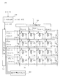
- FIG. 1 is a circuit diagram showing an electrical configuration of a liquid crystal display device according to a first embodiment of the present invention.
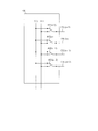
- FIG. 3 is a circuit diagram showing an electrical configuration of a storage capacitor line drive circuit in the first embodiment.
- (A) to (G) are voltage waveform diagrams for explaining the operation of the liquid crystal display device according to the first embodiment.
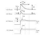
- FIG. 3A is a voltage waveform diagram of pixel potential obtained by enlarging a portion RB surrounded by a broken line in FIG.
- FIG. 5B is a voltage waveform diagram of the potential of the auxiliary capacitance line in the conventional liquid crystal display device in which a portion RA surrounded by a broken line in FIG.
- FIG. 3C is a voltage waveform diagram of the potential of the storage capacitor line in the first embodiment in which a portion RA surrounded by a broken line in FIG.
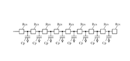
- FIG. 3 is an equivalent circuit diagram of the auxiliary capacitance line in the first embodiment.
- FIG. 3 is an equivalent circuit diagram of the auxiliary capacitance line in the first embodiment. It is a figure which shows the example which displayed the predetermined display pattern in the said 1st Embodiment.
- (A) to (D) are voltage waveform diagrams of portions corresponding to the scanning signal line GL (n) and the auxiliary capacitance line CSL (n) in the display image shown in FIG.
- (A) to (D) are voltage waveform diagrams of portions corresponding to the scanning signal line GL (p) and the auxiliary capacitance line CSL (p) in the display image shown in FIG.
- It is a circuit diagram which shows the electrical constitution of the liquid crystal display device which concerns on the 2nd Embodiment of this invention. It is a circuit diagram which shows the electrical constitution of the liquid crystal display device which concerns on the 3rd Embodiment of this invention. It is a circuit diagram which shows the electrical constitution of the liquid crystal display device which concerns on the 4th Embodiment of this invention. It is an equivalent circuit diagram of the auxiliary capacitance line in the fourth embodiment. It is a circuit diagram which shows the electrical constitution of the liquid crystal display device which concerns on the basic examination of this invention.
- FIG. 16A is a voltage waveform diagram of the potential of the auxiliary capacitance line obtained by enlarging a portion RA surrounded by a broken line in FIG.
- FIG. 16B is a voltage waveform diagram of pixel potential obtained by enlarging a portion RB surrounded by a broken line in FIG.
- FIG. 16A is a voltage waveform diagram of the potential of the auxiliary capacitance line obtained by enlarging a portion RA surrounded by a broken line in FIG.
- FIG. 16B is a voltage waveform diagram of pixel potential obtained by enlarging a portion RB surrounded by a broken line in FIG. (A) to (D) are voltage waveform diagrams for explaining the operation of the liquid crystal display device according to the basic examination according to the magnitude of the potential fluctuation amount ⁇ V. It is a figure which shows the example which displayed the predetermined display pattern in the liquid crystal display device which concerns on the said basic examination.
- FIG. (A) to (D) are voltage waveform diagrams of portions corresponding to the scanning signal line GL (n) and the auxiliary capacitance line CSL (n) in the display image shown in FIG. (A) to (D) are voltage waveform diagrams of portions corresponding to the scanning signal line GL (p) and the auxiliary capacitance line CSL (p) in the display image shown in FIG.
- FIG. 14 is a circuit diagram showing an electrical configuration of a conventional liquid crystal display device in which polarity inversion driving is performed by changing the potential of the corresponding auxiliary capacitance line after the end of the selection period of each scanning signal line.
- the conventional liquid crystal display device 690 includes a display panel 190, a data signal line driving circuit 200, a scanning signal line driving circuit 300, an auxiliary capacitance line driving circuit 400, and a display control circuit 500.
- the display panel 190 is composed of a pair of electrode substrates that sandwich a liquid crystal layer, and a polarizing plate is attached to the outer surface of each electrode substrate.
- One of the pair of electrode substrates is an active matrix substrate called a TFT (Thin Film Transistor) substrate.
- TFT substrate a plurality of data signal lines DL (1) to DL (M) (hereinafter referred to as “data signal lines DL” when not distinguished from each other) and a plurality of scans on an insulating substrate such as a glass substrate.
- the signal lines GL (1) to GL (N) are formed in a lattice shape so as to intersect with each other, and further, a plurality of scanning signal lines GL (1) to GL (N) (hereinafter referred to as “A plurality of auxiliary capacitance lines CSL (1) to CSL (N) (hereinafter referred to as “auxiliary capacitance line CSL” when they are not distinguished from each other). ”) Is formed.
- FIG. 14 shows only 16 pixel circuits, but in reality, N ⁇ M pixel circuits are formed on the display panel 190.
- the other of the pair of electrode substrates is called a counter substrate, and a counter electrode and an alignment film are sequentially stacked over an entire surface on an insulating substrate such as glass.
- the plurality of data signal lines DL (1) to DL (M), the plurality of scanning signal lines GL (1) to GL (N), and the plurality of auxiliary capacitance lines CSL (1) to CSL (N) are respectively data signal lines. It is driven by the drive circuit 200, the scanning signal line drive circuit 300, and the auxiliary capacitance line drive circuit 400.
- FIG. 15 is a circuit diagram showing an electrical configuration of the pixel circuit P (n, m).
- Each pixel circuit P (n, m) corresponds to one of intersections of the plurality of data signal lines DL (1) to DL (M) and the plurality of scanning signal lines GL (1) to GL (N). Is provided.
- Each pixel circuit P (n, m) has a source electrode connected to the data signal line DL (m) passing through the corresponding intersection and a gate electrode connected to the scanning signal line GL (n) passing through the corresponding intersection.
- the pixel TFT 101 and the pixel electrode connected to the drain electrode of the pixel TFT 101 are included.
- a liquid crystal capacitor Clc is formed by the pixel electrode and the counter electrode, and an auxiliary capacitor Ccs is formed by the pixel electrode and the auxiliary capacitor line CSL (n).
- the display control circuit 500 receives display data DAT and a timing control signal TS from the outside, and displays an analog image signal AV, a data start pulse signal SSP, a data clock as signals for causing the display panel 190 to display an image represented by the display data DAT.
- a signal SCK, a gate start pulse signal GSP, and a gate clock signal GCK are output.
- the data signal line driving circuit 200 receives the analog image signal AV, the data start pulse signal SSP, and the data clock signal SCK output from the display control circuit 500, and generates an analog image based on the data start pulse signal SSP and the data clock signal SCK.
- the signal AV is sequentially applied to each data signal line DL.
- the data signal line driving circuit 200 is driven by a so-called dot sequential driving method.
- the data signal line driving circuit 200 is not limited to the point sequential driving method, and the data signal line DL is grouped into a set including a predetermined number of data signal lines DL, and is shared by the predetermined number of data signal lines DL.
- the output buffer may be driven by a so-called SSD (Source Shared Driving) method, which is a method of driving each set by time-dividing a predetermined number of data signals corresponding to each set.
- the data signal line driving circuit 200 receives the digital image signal DV instead of the analog image signal AV, serial-parallel converts the digital image signal DV, and then generates a data signal by performing digital-analog conversion. .
- the scanning signal line driving circuit 300 sequentially supplies the plurality of scanning signal lines GL (1) to GL (N) by one horizontal scanning period. Then, an active scanning signal (voltage that makes the pixel TFT 101 included in the pixel circuit conductive) is applied to the selected scanning signal line.
- the auxiliary capacitance line driving circuit 400 outputs an auxiliary capacitance signal (predetermined low potential VL or predetermined high potential VH) that serves as a bias of a voltage to be applied to the liquid crystal layer of the display panel 190 to a plurality of auxiliary capacitance lines CSL (1) to Applied independently to CSL (N).
- auxiliary capacitance signal predetermined low potential VL or predetermined high potential VH
- the potential applied to the storage capacitor line is not limited to the two types of the low potential VL and the high potential VH. That is, three or more kinds of potentials may be used.
- the counter electrode is supplied with a potential Vcom serving as a reference for a voltage to be applied to the liquid crystal layer of the display panel 190 by a counter electrode driving circuit (not shown).
- a plurality of data signals are respectively applied to the plurality of data signal lines DL (1) to DL (M), and a plurality of scanning signals are applied to the plurality of scanning signal lines GL (1) to GL (N).
- the display panel 190 displays an image represented by the display data DAT by controlling the light transmittance of the liquid crystal layer by this applied voltage.
- the pixel circuits P (n, 1) to P (n) connected to the scanning signal line GL (n). , M) the pixel TFT 101 becomes conductive.
- a positive potential VdA as a data signal is applied to the pixel electrode from the data signal line DL (m), and the pixel capacitance is charged.
- the pixel potential Vd (n, m) is held at VdA (FIG. 16E).
- the scanning signal line GL (n) is in a non-selected state and the pixel TFT 101 connected to the scanning signal line GL (n) is cut off, the charge accumulated in the pixel capacitor is held as it is.
- the potential of the storage capacitor line CSL (n) is a predetermined low potential VL.
- the potential of the auxiliary capacitance line CSL (n) changes to a predetermined high potential VH.
- the high potential VH is applied to the storage capacitor line CSL (n), and the bias voltage ⁇ VlcP is applied to the pixel potential Vd (n, m).
- Vdpre (n, m) Vdpre (n, m) ⁇ Vdat (1)
- Vdpre (n, m) represents a pixel potential determined by changing the potential of the auxiliary capacitance line CSL (n) after the selection period of the scanning signal line GL (n) in the previous frame
- Vdat represents the next frame. Represents the voltage of the data signal to be written.
- the potential fluctuations of the pixel potentials Vd (n, 1) to Vd (n, m ⁇ 1) and Vd (n, m + 1) to Vd (n, M) are actually detected. Although affected, the illustration and description are omitted for convenience. Further, when the pixel TFT 101 is turned on by selecting the scanning signal line GL (n), the pixel potential Vd (n, n) is also influenced by the parasitic capacitance of the data signal lines DL (1) to (M). m) varies, but illustration and description thereof are omitted for convenience.
- the auxiliary capacitance line CSL (n) can be expressed by an equivalent circuit composed of a wiring resistance Rcs and a parasitic capacitance Cp.
- the auxiliary capacitance line CSL (n) in which the potential fluctuation ⁇ V has occurred attempts to return to the initial potential by charging / discharging the charge held in the parasitic capacitance Cp.
- the potential difference between the potential of the auxiliary capacitance line CSL (n) in which the potential variation ⁇ V has occurred and the initial potential from the time when the potential variation ⁇ V has occurred in the auxiliary capacitance line CSL (n) is a predetermined minute potential difference.
- the time until the point of time when ⁇ ( ⁇ 0 V) is referred to as “return time Tret”.
- the return time Tret depends on the resistance value of the wiring resistance Rcs, the capacitance value of the parasitic capacitance Cp, and the potential fluctuation amount ⁇ V. That is, when the potential fluctuation amount ⁇ V is considered to be constant, the return time Tret becomes longer as the time constant determined by the resistance value of the wiring resistance Rcs and the capacitance value of the parasitic capacitance Cp is larger.
- the auxiliary capacitance line drive circuit 400 requires a selection switch.
- the impedance of the auxiliary capacitance line CSL (n) further increases. Therefore, in the method of performing polarity inversion driving by changing the potential of the corresponding auxiliary capacitance line after the selection period of each scanning signal line is finished, the time constant is particularly large and the return time Tret is long.
- FIGS. 18A and 18B show the potential of the auxiliary capacitance line CSL (n) obtained by enlarging the portion RA surrounded by the broken line in FIG. 16C when Twrt> Tret, and FIG. It is a voltage waveform diagram of the pixel potential Vd (n, m) obtained by enlarging a portion RB surrounded by a broken line in E).
- Twrt represents a writing period of the pixel potential Vd (n, m).
- the potential of the auxiliary capacitance line CSL (n) is restored within the writing period Twrt of the pixel potential Vd (n, m). In this case, the pixel potential Vd (n, m) is not affected by the potential fluctuation of the storage capacitor line CSL (n).
- FIGS. 19A and 19B show the potential of the auxiliary capacitance line CSL (n) obtained by enlarging the portion RA surrounded by the broken line in FIG. 16C when Twrt ⁇ Tret, and FIG. It is a voltage waveform diagram of the pixel potential Vd (n, m) obtained by enlarging a portion RB surrounded by a broken line in E).
- the potential of the auxiliary capacitance line CSL (n) does not return within the writing period Twrt of the pixel potential Vd (n, m).
- FIG. 20A and 20C are voltage waveform diagrams (in the case where the potential fluctuation amount ⁇ V is large) in which the portions RA and RB surrounded by the broken line in FIG. 16 are enlarged.
- FIG. 20B and FIG. 20D are voltage waveform diagrams (in the case where the voltage fluctuation amount ⁇ V is small), respectively, in which the portion RA and RB enlarged by the broken line in FIG.
- the above-described influence of the residual voltage ⁇ Vcs received by the pixel potential Vd (n, m) is particularly noticeable in a display pattern including a gray background portion and a white central portion as shown in FIG.
- a gray background portion is represented by thin line hatching
- a blackened portion described later is represented by thick line hatching.
- the size of each pixel is non-uniform for convenience of explanation.
- a downward arrow and a right arrow in FIG. 21 represent a vertical scanning direction and a horizontal scanning direction in image display, respectively. All the pixels corresponding to the scanning signal line GL (n) and the auxiliary capacitance line CSL (n) are gray, and display unevenness does not occur.
- the pixels corresponding to the scanning signal line GL (p) and the auxiliary capacitance line CSL (p) are gray or white, and the pixel corresponding to the data signal line DL (m + 2) should be gray, so that horizontal crosstalk occurs. Doing so makes it dark.
- the lateral crosstalk will be further described with reference to FIGS. 21, 22A to 22D, and FIGS. 23A to 23D.
- FIGS. 22A to 22D are voltage waveform diagrams of the pixel potentials Vd (n, m) to Vd (n, m + 2) and the auxiliary capacitor line CSL (n) in FIG. 21, respectively.
- Vd (n, m) to Vd (n, m + 2) shown in FIGS. 22A to 22C potential fluctuations of the auxiliary capacitance line CSL (n) before each writing period Twrt.
- ⁇ V is omitted for convenience (the same applies to FIGS. 8A to 8C described later).
- FIG. 8A to 8C described later.
- the pixel potentials Vd (n, 1) to Vd (n, m ⁇ 1) and Vd (n, m + 3) to Vd (n, m ) Is omitted for convenience (the same applies to FIG. 8D described later). Since the pixels corresponding to the pixel potentials Vd (n, m) to Vd (n, m + 2) are all gray, the write potentials of the pixel potentials Vd (n, m) to Vd (n, m + 2) are the same VdA. . For this reason, the potential fluctuation amount ⁇ V in the auxiliary capacitance line CSL (n) generated when writing each pixel potential is uniform. Therefore, horizontal crosstalk does not occur in the pixels corresponding to the scanning signal line GL (n) and the auxiliary capacitance line CSL (n).
- FIGS. 23A to 23D are voltage waveform diagrams of the pixel potentials Vd (p, m) to Vd (p, m + 2) and the auxiliary capacitor line CSL (p) in FIG. 21, respectively.
- Vd (p, m) to Vd (p, m + 2) shown in FIGS. 23A to 23C potential fluctuations of the auxiliary capacitance line CSL (n) before each writing period Twrt.
- ⁇ V is omitted for convenience (the same applies to FIGS. 9A to 9C described later).
- the pixel potentials Vd (p, 1) to Vd (p, m-1) and Vd (p, m + 3) to Vd (p, m ) Is omitted for convenience (the same applies to FIG. 9D described later).
- Pixels corresponding to the pixel potentials Vd (p, m) and Vd (p, m + 2) are gray, and pixels corresponding to the pixel potential Vd (p, m + 1) are white.
- the writing potential of Vd (p, m) and Vd (p, m + 2) is VdA
- the writing potential of the pixel potential Vd (p, m + 1) is VdB (> VdA).
- the potential fluctuation amount ⁇ V in the auxiliary capacitance line CSL (p) generated when the pixel potentials Vd (p, m) and Vd (p, m + 2) are written is small, and the auxiliary capacitance generated when the pixel potential Vd (p, m + 1) is written.
- the potential fluctuation amount ⁇ V in the line CSL (p) is large.
- the pixel potential Vd (p, m + 2) becomes VdA ⁇ Vd, which is a value different from the potential VdA that should be originally held, and the corresponding pixel becomes darker than the gray that should be originally displayed.
- the pixel potential Vd (p, m + 1) corresponding to white display also has a value different from the potential VdB that should be originally held and becomes darker than the original.
- Patent Document 5 discloses an example in which an auxiliary capacitor for voltage stabilization is formed using a common auxiliary capacitor line. However, this also requires a wide area, and the aperture ratio decreases. End up.
- FIG. 1 is a circuit diagram showing an electrical configuration of the liquid crystal display device according to the first embodiment of the present invention. Note that, among the constituent elements of this embodiment, the same elements as those of the conventional liquid crystal display device 690 are denoted by the same reference numerals and description thereof is omitted.
- the liquid crystal display device 600 according to this embodiment includes a display panel 100, a data signal line driving circuit 200, a scanning signal line driving circuit 300, an auxiliary capacitance line driving circuit 400, and a display control circuit 500. ing.
- any or all of the data signal line driving circuit 200, the scanning signal line driving circuit 300, the auxiliary capacitance line driving circuit 400, and the display control circuit 500 are mounted on the TFT substrate of the display panel 100 as an IC (Integrated Circuit), for example. Has been.
- any or all of the data signal line driving circuit 200, the scanning signal line driving circuit 300, and the storage capacitor line driving circuit 400 may be formed integrally with the display panel 100.
- the scanning signal line driver circuit 300 receives the gate start pulse GSP and the gate clock signal GCK from the display control circuit 500, and performs a plurality of scans in each frame period (each vertical scanning period) for displaying a display image on the display panel 100.
- the signal lines GL (1) to GL (N) are sequentially selected for each horizontal scanning period, and an active scanning signal (a voltage for bringing the pixel TFT 101 included in the pixel circuit into a conductive state) is applied to the selected scanning signal line.
- scanning is performed in ascending order of the numbers of the scanning signal lines GL. That is, the scanning signal lines are selected in the order of GL (1) ⁇ GL (2) ⁇ ... ⁇ GL (N). In this specification, such a scanning direction is referred to as a “first direction”.
- the auxiliary capacitance line driving circuit 400 outputs an auxiliary capacitance signal (predetermined low potential VL or predetermined high potential VH) serving as a bias of a voltage to be applied to the liquid crystal layer of the display panel 100 to a plurality of auxiliary capacitance lines CSL (1) ⁇ Applied independently to CSL (N). Specifically, as shown in FIG. 2, the auxiliary capacitance line driving circuit 400 switches the potential to be applied to the auxiliary capacitance lines CSL (1) to CSL (N) between the low potential VL and the high potential VH. Switches 402 (1) to 402 (N) are included.
- the display panel 100 includes an output end side as an output end side switching element provided on the output end side of the scanning signal lines GL (1) to GL (N) in the display panel 190 provided in the conventional liquid crystal display device 690.
- TFTs 12 (1) to 12 (N) (hereinafter referred to as “output end side TFT 12” when these are not distinguished) are added.
- the storage capacitor lines CSL adjacent to each other are connected to each other on the output end side via the output end side TFT 12.
- the auxiliary capacitance lines CSL (n ⁇ 1) and CSL (n) are connected to each other on the output end side via the output end side TFT 12 (n).
- the gate electrode as the control terminal of each output terminal side TFT 12 is connected to the corresponding scanning signal line GL, and the source electrode as one of the conduction terminals of each output terminal side TFT 12 is disposed along the corresponding scanning signal line GL.
- the drain electrode as the other of the conduction terminals of each output terminal side TFT 12 is connected to the auxiliary capacitance line CSL and the auxiliary capacitance line CSL arranged along the preceding scanning signal line in the first direction of the corresponding scanning signal line GL. It is connected to the.
- the gate electrode of the output end side TFT 12 (n) is connected to the scanning signal line GL (n)
- the source electrode is connected to the auxiliary capacitance line CSL (n) arranged along the scanning signal line GL (n).
- the drain electrode is connected to the auxiliary capacitance line CSL (n ⁇ 1) disposed along the preceding scanning signal line GL (n ⁇ 1) in the first direction of the scanning signal line GL (n).
- the source electrode and the drain electrode of the corresponding output terminal side TFT 12 are interchanged depending on the potential of each auxiliary capacitance line CSL, but in the following description, along the scanning signal line GL to which the gate electrode of the output terminal side TFT 12 is connected.
- the terminal connected to the arranged auxiliary capacitance line CSL is a source electrode, and the side connected to the auxiliary capacitance line CSL arranged along the preceding scanning signal line GL in the scanning direction of the scanning signal line GL. These terminals are used as drain electrodes.
- Each output end side TFT 12 is controlled so as to be in a conductive state when the scanning signal line GL connected to the gate electrode is in a selected state and into a blocked state when it is in a non-selected state.
- the output end side TFT 12 (n) is controlled so as to be in a conductive state if the scanning signal line GL (n) connected to the gate electrode is in a selected state and in a blocked state if it is in a non-selected state.
- 3A to 3G respectively show the potential of the scanning signal line GL (n ⁇ 1) and the scanning signal line in the first frame period TF1 and the second frame period TF2, which are two consecutive frame periods.
- the polarity based on the counter electrode potential Vcom of the data signal to be applied to the data signal lines DL (1) to DL (m) is set to one horizontal.
- Vcom a 1H inversion driving method in which inversion is performed every period is employed and display is performed in a normally black mode.
- Vcom 0, it is not limited to this.
- FIG. 4A to 4C show the pixel potential Vd (n, m) obtained by enlarging the portion RB surrounded by the broken line in FIG. 3G and the portion RA surrounded by the broken line in FIG.
- the potential of the storage capacitor line CSL ′ (n) in the enlarged conventional liquid crystal display device and the potential of the storage capacitor line CSL (n) in this embodiment in which the portion RA surrounded by the broken line in FIG. It is a voltage waveform diagram.
- the pixel circuits P (n, 1) to P (n) connected to the scanning signal line GL (n). , M) the pixel TFT 101 becomes conductive.
- the output end side TFT 12 (n) becomes conductive.
- the storage capacitor line CSL (n ⁇ 1) disposed along the preceding scanning signal line GL (n ⁇ 1) in the direction is connected.
- the auxiliary capacitance lines CSL (n ⁇ 1) to CSL (n + 1) at this time are expressed by an equivalent circuit including the wiring resistance Rcs and the parasitic capacitance Cp shown in FIG.
- the potentials applied to the storage capacitor line CSL (n ⁇ 1) and the storage capacitor line CSL (n) are both low potential VL, and the potential applied to the storage capacitor line CSL (n + 1) is a high potential. VH.
- the auxiliary capacitance lines CSL (n ⁇ 1) and CSL (n) are connected to each other via the output end side TFT 12 (n) (on-resistance RAon) that has become conductive.
- the pixel electrode In the writing period for the pixel circuit P (n, m), the pixel electrode is charged with a positive potential VdA as a data signal from the data signal line DL (m) to the pixel electrode.
- VdA positive potential
- the potential fluctuation of the pixel potential Vd (n, m) generated when the data signal is written to the pixel electrode is transmitted to the auxiliary capacitance line CSL (n) through the parasitic capacitance Cdc.
- a potential fluctuation ⁇ V occurs in the storage capacitor line CSL (n) (a portion RA surrounded by a broken line in FIG. 3E). As shown in FIGS.
- the potential fluctuation ⁇ V occurs when the pixel potential Vd (n, m) changes in polarity. Has occurred (indicated by a straight line in the figure).
- the potential fluctuations of the pixel potentials Vd (n, 1) to Vd (n, m ⁇ 1) and Vd (n, m + 1) to Vd (n, M) are actually detected. Although affected, the illustration and description are omitted for convenience.
- the pixel potential Vd (n, n) is also influenced by the parasitic capacitance of the data signal lines DL (1) to (M). m) varies, but illustration and description thereof are omitted for convenience.
- PA a portion near the output end indicated by PA in FIG. 5 (hereinafter simply referred to as “PA”).
- PA potential fluctuation
- the final charge / discharge destination for convergence of the potential fluctuation ⁇ V generated in PA is only in the direction in which the potential changeover switch 402 (n) is connected.
- the auxiliary capacitance lines CSL (n) and CSL (n ⁇ 1) are connected via the output end side TFT 12 (n).
- the final charge / discharge destination for convergence of the potential fluctuation ⁇ V generated in PA is the direction in which the potential changeover switch 402 (n) is connected and the potential changeover switch 402 (n ⁇ 1).
- the impedance viewed from the PA is apparently reduced to about half of the conventional one (the time constant is about half).
- the apparent impedance reduction rate decreases with increasing distance from the PA in the direction in which the potential changeover switch 402 (n) is connected.
- the “impedance reduction rate” means a ratio of the impedance in the present embodiment reduced with respect to the impedance in the conventional liquid crystal display device.
- the residual voltage ⁇ Vcs which is the difference between the potential of the auxiliary capacitance line CSL (n) at the end of the writing period Twrt and the original potential of the auxiliary capacitance line CSL (n) does not occur, so the pixel potential Vd (n, m) Holds the potential VdA that should originally be held (FIGS. 3G and 4A).
- 3G is applied to the portion of the liquid crystal layer sandwiched between the pixel electrode and the counter electrode, and the charge is held until the pixel TFT 101 becomes conductive again.
- a large voltage can be applied to the liquid crystal layer with a small data signal amplitude, so that power consumption can be reduced.
- the pixel circuits P (n + 1,1) to P (n + 1, M) connected to the scanning signal line GL (n + 1) The pixel TFT 101 becomes conductive. At this time, the output end side TFT 12 (n + 1) is in a conductive state.
- the storage capacitor line CSL (n) disposed along the preceding scanning signal line GL (n) in the direction is connected.
- the auxiliary capacitance lines CSL (n ⁇ 1) to CSL (n + 1) at this time are expressed by an equivalent circuit including the wiring resistance Rcs and the parasitic capacitance Cp shown in FIG.
- the potential applied to the auxiliary capacitance line CSL (n ⁇ 1) is the low potential VL
- the potentials applied to the auxiliary capacitance lines CSL (n) and CSL (n + 1) are both the high potential VH.
- the auxiliary capacitance lines CSL (n) and CSL (n + 1) are connected to each other via the output end side TFT 12 (n + 1) (ON resistance Ron) that is turned on.
- the impedance viewed from the PB is apparently about half that of the conventional one, as in the above-described PA. Since the subsequent operation is the same as that described above, the description thereof is omitted.
- FIG. 7 is a diagram illustrating a display pattern similar to the display pattern including the gray background portion and the white center portion illustrated in FIG. 21 in the present embodiment.
- the gray background portion is indicated by hatching.
- the size of each pixel is not uniform for convenience of explanation.
- a downward arrow and a right arrow in FIG. 7 represent a vertical scanning direction and a horizontal scanning direction in image display, respectively.
- FIG. 8A to 8D are voltage waveform diagrams of the pixel potentials Vd (n, m) to Vd (n, m + 2) and the auxiliary capacitance line CSL (n) in FIG. 7, respectively. Since the pixels corresponding to the pixel potentials Vd (n, m) to Vd (n, m + 2) are all gray, the write potentials of the pixel potentials Vd (n, m) to Vd (n, m + 2) are the same VdA. . For this reason, the amount of potential fluctuation in the auxiliary capacitance line CSL (n) generated when writing each pixel potential is uniform.
- FIGS. 9A to 9D are voltage waveform diagrams of the potentials of the pixel potentials Vd (p, m) to Vd (p, m + 2) and the auxiliary capacitance line CSL (p) in FIG. 7, respectively.
- Pixels corresponding to the pixel potentials Vd (p, m) and Vd (p, m + 2) are gray, and pixels corresponding to the pixel potential Vd (p, m + 1) are white.
- the writing potential of Vd (p, m) and Vd (p, m + 2) is VdA
- the writing potential of the pixel potential Vd (p, m + 1) is VdB (> VdA).
- the potential fluctuation amount ⁇ V in the auxiliary capacitance line CSL (p) generated when the pixel potentials Vd (p, m) and Vd (p, m + 2) are written is small, and the auxiliary capacitance generated when the pixel potential Vd (p, m + 1) is written.
- the potential fluctuation amount ⁇ V in the line CSL (p) is large.
- the apparent impedance of the storage capacitor line CSL is reduced as described above. Therefore, unlike the conventional liquid crystal display device 690, even if the potential of the auxiliary capacitor CSL (p) greatly fluctuates when the potential Vd (p, m + 1) is written, the potential before the pixel potential Vd (p, m + 2) is written.
- the changed potential returns to the original potential, and the potential of the auxiliary capacitance line CSL (p) at the start of writing of the pixel potential Vd (p, m + 2) does not occur. Therefore, the potential fluctuation of the auxiliary capacitance line CSL (p) that occurs when the pixel potential Vd (p, m + 2) is written is also eliminated during the writing period, so that the residual voltage ⁇ Vcs does not occur. As a result, the pixel potential Vd (p, m + 2) is held at VdA, which is the original writing potential, so that the pixel corresponding to the pixel potential Vd (p, m + 2) is the same gray as the color to be originally displayed and is blackish Don't be. As described above, in the display pattern displayed on the liquid crystal display device 600 according to the present embodiment, the horizontal crosstalk does not occur unlike the display pattern displayed on the conventional liquid crystal display device.
- the scanning signal line GL (n) is selected along the scanning signal line GL (n) when the scanning signal line GL (n) is selected.
- the auxiliary capacitance line CSL (n) arranged is connected to the CSL (n ⁇ 1) arranged along the preceding scanning signal line GL (n ⁇ 1) in the scanning direction of the scanning signal line GL (n).
- the apparent impedance of the auxiliary capacitance line CSL (n) is reduced as compared with the conventional case.
- the time Tret until the potential of the storage capacitor line CSL (n) that has fluctuated at the time of writing the data signal returns to the original potential is shorter than before.
- the pixel potential Vd (n, m) does not vary due to the potential variation of the auxiliary capacitance line CSL (n).
- a dummy auxiliary capacitance line CSL (0) may be provided in front of the auxiliary capacitance line CSL (1) in order to sufficiently suppress potential fluctuations in the auxiliary capacitance line CSL (1).
- the drain electrode of the output end side TFT 12 (1) is connected to the auxiliary capacitance line CSL (0).
- FIG. 10 is a circuit diagram showing an electrical configuration of a liquid crystal display device 610 according to the second embodiment of the present invention.
- the liquid crystal display device 610 according to the present embodiment includes the display panel 110 instead of the display panel 100, and has the same configuration as the liquid crystal display device 600 according to the first embodiment except for the scanning direction of the scanning signal lines GL. It is.
- the same elements as those of the first embodiment are denoted by the same reference numerals and description thereof is omitted.
- scanning is performed in ascending order of the numbers of the scanning signal lines GL.
- scanning is performed in descending order of the numbers of the scanning signal lines GL. That is, the scanning signal line GL is selected in the order of GL (N) ⁇ GL (N ⁇ 1) ⁇ ... ⁇ GL (1).
- the scanning direction opposite to the first direction is referred to as a “second direction”.
- the display panel 110 in the present embodiment is different from the display panel 100 in the first embodiment in the connection method of the output terminal side TFTs 12. That is, the gate electrode as the control terminal of each output terminal side TFT 12 is connected to the corresponding scanning signal line GL, and the source electrode as one of the conduction terminals of each output terminal side TFT 12 is arranged along the corresponding scanning signal line GL.
- the drain electrode as the other conductive terminal of each output terminal side TFT 12 is connected to the auxiliary capacitance line CSL, and the auxiliary capacitance line arranged along the preceding scanning signal line in the second direction of the corresponding scanning signal line Connected to CSL.
- the gate electrode of the output end side TFT 12 (n) is connected to the scanning signal line GL (n), and the source electrode is connected to the auxiliary capacitance line CSL (n) arranged along the scanning signal line GL (n).
- the drain electrode is connected to the preceding scanning signal line GL (n + 1) in the second direction of the scanning signal line GL (n).
- the direction of the current flowing through the output end side TFT 12 (n) is opposite to that in the first embodiment. Therefore, the source electrode and the drain electrode are reversed in this embodiment and the first embodiment. It has become.
- each output-end TFT 12 is controlled so as to be in a conductive state if the scanning signal line GL connected to the gate electrode is in a selected state, and in a blocked state if it is in a non-selected state.
- the output end side TFT 12 (n) is controlled so as to be in a conductive state if the scanning signal line GL (n) connected to the gate electrode is in a selected state and in a blocked state if it is in a non-selected state.
- the operation of the liquid crystal display device 610 according to the present embodiment is the same as that of the first embodiment except that the scanning direction is the second direction, and a description thereof will be omitted.
- a dummy auxiliary capacitance line CSL (N + 1) may be provided at the subsequent stage of the auxiliary capacitance line CSL (N) in order to sufficiently suppress the potential fluctuation in the auxiliary capacitance line CSL (N).
- the drain electrode of the output end side TFT (N) is connected to the auxiliary capacitance line CSL (N + 1).
- FIG. 11 is a circuit diagram showing an electrical configuration of a liquid crystal display device 620 according to the third embodiment of the present invention.
- the liquid crystal display device 620 according to this embodiment includes a scanning signal line driving circuit 310 capable of bidirectional scanning instead of the scanning signal line driving circuit 300, and an auxiliary capacitance line driving instead of the auxiliary capacitance line driving circuit 400.
- the configuration is the same as that of the liquid crystal display device 600 according to the first embodiment except that the circuit 410 is provided and the display panel 120 is provided instead of the display panel 100.
- the same elements as those of the first embodiment are denoted by the same reference numerals and description thereof is omitted.
- the scanning signal line drive circuit 310 in the present embodiment is configured to be able to switch the scanning direction of the scanning signal line GL between the first direction and the second direction. This switching is performed based on a scanning direction control signal UD given from the outside. For example, when a predetermined high potential UDH is applied as the scanning direction control signal UD, the scanning direction is the first direction, and when a predetermined low potential UDL is applied as the scanning direction control signal UD, the scanning direction is the second direction.
- FIG. 11 shows an example when the high potential UDH is given as the scanning direction control signal UD (when the scanning direction is the first direction).
- the auxiliary capacitance line driving circuit 410 provides the auxiliary capacitance signals to be given to the auxiliary capacitance lines CSL (1) to CSL (N) in accordance with the scanning direction (first direction or second direction) of the scanning signal line GL.
- the order in which the potentials of these are changed can be switched. This switching is performed based on a scanning direction control signal UD given from the outside, similarly to switching of the scanning direction in the scanning signal line driving circuit 310.
- the display panel 120 includes scanning signal line switching provided corresponding to the scanning signal lines GL (1) to GL (N) in addition to the components included in the display panel 100 according to the first embodiment. It further includes switches 22 (1) to 22 (N) (hereinafter referred to as “scanning signal line switch 22” when these are not distinguished).
- the switching terminal NA as one of the switching terminals of each scanning signal line switch 22 is connected to the corresponding scanning signal line GL, and the switching terminal NB as the other of the switching terminals is in the first direction of the corresponding scanning signal line GL.
- the common terminal NC is connected to a gate electrode as a control terminal of each output terminal side TFT 12.
- the switching terminal NA of the scanning signal line switch 22 (n) is connected to the corresponding scanning signal line GL (n), and the switching terminal NB is the preceding scanning signal line in the first direction of the scanning signal line GL (n).
- the common terminal NC is connected to the gate electrode of the output end side TFT 12 (n).
- Each scanning signal line change-over switch 22 is controlled by a scanning direction control signal UD.
- each scanning signal line change-over switch 22 is controlled to select the switching terminal NA.
- the scanning signal line changeover switch 22 (n) selects the switching terminal NA
- the gate electrode of the output terminal side TFT 12 (n) is connected to the corresponding scanning signal line GL (n)
- the output terminal Of the input / output terminals of the side TFT 12 (n) is the source electrode
- the side connected to the auxiliary capacitance line CSL (n ⁇ 1) is the drain electrode.
- each scanning signal line change-over switch 22 is controlled to select the switching terminal NB.
- each scanning signal line changeover switch 22 selects the switching terminal NB, whereby the gate electrode of the output terminal side TFT 12 (n) is connected to the corresponding scanning signal line GL (n ⁇ 1), and the output terminal Of the input / output terminals of the side TFT 12 (n), the side connected to the auxiliary capacitance line CSL (n) is the drain electrode, and the side connected to the auxiliary capacitance line CSL (n ⁇ 1) is the source electrode.
- the output end side TFT 12 (n ⁇ 1) corresponding to the scanning signal line GL (n) corresponds to the output end side TFT 12 (n) in the second embodiment.
- the connection of the output terminal side TFTs 12 is the same as that in the second embodiment.
- the operation of the liquid crystal display device 620 according to the present embodiment is the same as that of the liquid crystal display device 600 according to the first embodiment when the high potential UDH is applied as the scanning direction control signal UD, and the scanning direction control signal UD.
- the operation is the same as that of the liquid crystal display device 610 according to the second embodiment.
- a dummy storage capacitor line CSL (0) may be provided before the line CSL (1).
- the drain electrode of the output end side TFT 12 (1) is connected to the auxiliary capacitance line CSL (0).
- FIG. 12 is a circuit diagram showing an electrical configuration of a liquid crystal display device 630 according to the fourth embodiment of the present invention.
- the liquid crystal display device 630 according to the present embodiment has the same configuration as the liquid crystal display device 600 according to the first embodiment, except that the display panel 130 is provided instead of the display panel 100.
- the same elements as those of the first embodiment are denoted by the same reference numerals and description thereof is omitted.
- the display panel 130 according to the present embodiment has an input end side as an input end side switching element provided on the display panel 100 according to the first embodiment in correspondence with the scanning signal lines GL (1) to GL (N). TFTs 14 (1) to 14 (N) (hereinafter referred to as “input end side TFT 14” when these are not distinguished) are added.
- the storage capacitor lines CSL adjacent to each other are connected to each other on the input end side via the input end side TFT 14.
- the auxiliary capacitance lines CSL (n ⁇ 1) and CSL (n) are connected on the input end side via the input end side TFT 14 (n).
- the adjacent auxiliary capacitance lines CSL are connected to each other not only through the output end side TFT 12 but also through the input end side TFT 14.
- the gate electrode as the control terminal of each input end side TFT 14 is connected to the corresponding scanning signal line GL, and the source electrode as one of the conduction terminals of each input end side TFT 14 is arranged along the corresponding scanning signal line GL.
- the drain electrode as the other end of each input end side TFT 14 connected to the auxiliary capacitance line CSL is connected to the auxiliary capacitance line CSL arranged along the preceding scanning signal line in the first direction of the corresponding scanning signal line GL.
- the gate electrode of the input end side TFT 14 (n) is connected to the scanning signal line GL (n)
- the source electrode is connected to the auxiliary capacitance line CSL (n) arranged along the scanning signal line GL (n).
- the drain electrode is connected to the auxiliary capacitance line CSL (n ⁇ 1) disposed along the preceding scanning signal line GL (n ⁇ 1) in the first direction of the scanning signal line GL (n).
- Each input terminal side TFT 14 is controlled so as to be in a conductive state when the scanning signal line GL connected to the gate electrode is in a selected state and into a blocked state when it is in a non-selected state.
- the input end side TFT 14 (n) is controlled so as to be in a conductive state if the scanning signal line GL (n) connected to the gate electrode is in a selected state, and in a blocked state if it is in a non-selected state.
- auxiliary capacitance line CSL (n) arranged along the scanning signal line GL (n) in the selected state and the scanning signal
- the storage capacitor line CSL (n ⁇ 1) arranged along the preceding scanning signal line GL (n ⁇ 1) in the first direction of the line GL (n) is connected.
- the auxiliary capacitance lines CSL (n ⁇ 1) to CSL (n + 1) at this time are expressed by an equivalent circuit including the wiring resistance Rcs and the parasitic capacitance Cp shown in FIG.
- auxiliary capacitance lines CSL (n ⁇ 1) and CSL (n) are connected to each other through the output end side TFT 12 (n) (on resistance RAon) and the input end side TFT 14 (n) (on resistance RBon) that are turned on. Are connected to each other.
- the final charging / discharging destination for converging the potential fluctuation ⁇ V generated in the PA is in two directions, so that the impedance viewed from the PA apparently becomes about half of the conventional one.
- the apparent impedance reduction rate decreases as the distance from the PA increases in the direction in which the potential changeover switch 402 (n) is connected.
- PC PC in FIG. 13
- the auxiliary capacitance lines CSL (n ⁇ 1) and CSL (n) are connected via the input end side TFT 14 (n) (ON resistance RBon), so that only the impedance viewed from the PA is obtained.
- the impedance viewed from the PC is apparently about half that of the conventional one (the time constant is about half).
- the apparent impedance between the PC and the PA is also reduced as compared with the first embodiment.
- the apparent impedance of the auxiliary capacitance line CSL (n) is sufficiently reduced as compared with the conventional case regardless of the position where the potential fluctuation ⁇ V of the auxiliary capacitance line CSL (n) occurs. For this reason, the time Tret until the potential of the auxiliary capacitance line CSL (n) changed at the time of writing the data signal returns to the original potential regardless of the position where the potential change ⁇ V of the auxiliary capacitance line CSL (n) occurs is conventionally. Is also sufficiently short.
- a dummy auxiliary capacitance line CSL (0) may be provided in front of the auxiliary capacitance line CSL (1) in order to sufficiently suppress potential fluctuations in the auxiliary capacitance line CSL (1).
- the drain electrode of the output end side TFT 12 (1) and the drain electrode of the input end side TFT 14 (1) are connected to the auxiliary capacitance line CSL (0).
- Each output end side TFT 12 and each input end side TFT 14 are preferably formed integrally on the TFT substrate of the display panel 100. In each of the above embodiments, each output end side TFT 12 and each input end side TFT 14 are controlled by the potential of the corresponding scanning signal line GL. However, the present invention is not limited to this. Also good.
- Input end side TFTs 14 (1) to 14 (N) may be added to the liquid crystal display device according to the second embodiment or the third embodiment. Thereby, lateral crosstalk can be more reliably suppressed.
- the low potential VH and the high potential VH are used, but three or more types may be used.
- the scanning signal line GL is in the selected state, it is desirable that the potentials of the two auxiliary capacitance lines CSL connected via the output end side TFT 12 or the input end side TFT 14 in the conductive state are the same potential.
- the present invention can be applied to an active matrix display device using a switching element such as a thin film transistor.
Landscapes
- Engineering & Computer Science (AREA)
- Chemical & Material Sciences (AREA)
- Crystallography & Structural Chemistry (AREA)
- Physics & Mathematics (AREA)
- Computer Hardware Design (AREA)
- General Physics & Mathematics (AREA)
- Theoretical Computer Science (AREA)
- Power Engineering (AREA)
- Control Of Indicators Other Than Cathode Ray Tubes (AREA)
Abstract
簡易な構成で横クロストークを抑制できる表示装置を提供する。 液晶表示装置(600)の備える表示パネル(100)は、走査信号線(GL)の出力端側に設けられた走出力端側TFT(12)を含んでいる。出力端側TFT(12)を介して、互いに隣接する補助容量線(CSL)が接続されている。走査信号線(GL)が選択状態となると、対応する出力端側TFT(12)が導通状態となることにより補助容量線(CSL)とその先行の補助容量線(CSL)とが接続される。このとき、補助容量線(CSL)で電位変動が生じた位置から見たインピーダンスが見かけ上従来よりも低減される。そのため、データ信号の書き込み時に変動した補助容量線(CSL)の電位が本来の電位に復帰するまでの時間Tretが従来よりも短くなる。
Description
本発明は、表示装置に関し、特に、薄膜トランジスタ等のスイッチング素子を用いたアクティブマトリクス型の表示装置に関する。
近年、液晶表示装置および有機EL表示装置等のアクティブマトリクス型表示装置が広く普及している。特に、薄膜トランジスタ(Thin Film Transistor:TFT)等のスイッチング素子が画素回路毎に設けられた液晶表示装置は、画素数が増大してもクロストークの少ない表示画像を得ることができるため、注目を集めている。
このようなアクティブマトリクス型の液晶表示装置に関して、従来から低消費電力化が求められている。この低消費電力化を図る方法の1つとして、各走査信号線の選択期間終了後に対応する補助容量線の電位を変化させることにより極性反転駆動を行う方法が知られている。このような駆動方法によれば、小さなデータ信号振幅で液晶層に大きな電圧を加えることができるので、消費電力を低減することができる。このような駆動方法は、例えば、特許文献1~3に開示されている。
しかし、補助容量線の電位を変化させることにより極性反転駆動を行う液晶表示装置では画素電極と補助容量線とによって補助容量が形成されるので、データ信号を画素電極に書き込む際に生じる画素電極の電位変動が、補助容量を介して補助容量線に伝達されてしまう。これにより、補助容量線の電位が変動し、その結果、画素電位が本来保持されるべき電位と異なる値となってしまう。そのため、各走査信号線の選択期間終了後に対応する補助容量線の電位を変化させることにより極性反転駆動を行う方法を用いた従来の液晶表示装置では、横方向のクロストーク(以下、「横クロストーク」という)が生じ、表示品位が低下するという問題があった。
このような横クロストークを解消する方法として、特許文献4には、補助容量線の両端側にそれぞれ補助容量線駆動回路が設けられ、上述のように各走査信号線の選択期間終了後に対応する補助容量線の電位を変化させることにより極性反転駆動を行う表示装置が開示されている。このように、補助容量線の両端側から電位を供給することにより、補助容量線の見かけ上のインピーダンスを下げることができる。これにより、補助容量線の電位が変動した場合でもその変動を抑制することができる。また、特許文献5には、各補助容量線に電圧安定化用の補助容量が設けられた表示装置が開示されている。この電圧安定化用の補助容量により、各補助容量に混入するノイズを吸収することができる。これにより、補助容量線の電位変動を抑制することができる。その他、本願発明に関連した表示品位の低下を抑制する手段などは、例えば特許文献6~8に開示されている。
しかし、上記特許文献4に記載の表示装置の構成では、補助容量線の両端側に補助容量線駆動回路が必要となるので回路規模が大きくなる。そのため、狭額縁化が困難であると共に、消費電力が増大してしまう。また、補助容量線の両端側から電位を供給するので、補助容量電位の振幅が増大することにより消費電力が増大してしまうおそれがある。このため、補助容量線の両端側からの電位供給のタイミングを合わせる必要がある。
また、上記特許文献5に記載の表示装置の構成では、上述の効果を十分に得るためには大容量の電圧安定化用の補助容量が必要となる。そのため、電圧安定化用の補助容量を設けるための広い領域が必要となり、開口率が低下してしまう。なお、上記特許文献5には、共通補助容量線を利用して電圧安定化用の補助容量を形成する例が開示されているが、これによってもなお広い領域が必要となり、開口率が低下してしまう。
そこで、本発明は、簡易な構成で横クロストークを抑制できる表示装置を提供することを目的とする。
本発明の第1の局面は、表示装置であって、
表示すべき画像を表す複数のデータ信号がそれぞれ印加される複数のデータ信号線と、
前記複数のデータ信号線と交差し、複数の走査信号がそれぞれ印加されることにより選択的に駆動される走査信号線と、
前記複数のデータ信号線と前記複数の走査信号線との交差点にそれぞれ対応してマトリクス状に配置された複数の画素回路と、
前記複数の走査信号線にそれぞれ沿って配置された複数の補助容量線と、
前記複数の補助容量線を互いに独立して駆動するための複数の補助容量信号を前記複数の補助容量線にそれぞれ印加する補助容量線駆動回路と、
各走査信号線の出力端側に設けられた出力端側スイッチング素子とを備え、
各画素回路は、
対応する交差点を通過する走査信号線が選択状態のときに導通状態、非選択状態のときに遮断状態となる画素スイッチング素子と、
対応する交差点を通過するデータ信号線に前記画素スイッチング素子を介して接続された画素電極と、
前記複数の画素回路に共通的に設けられた共通電極と、
前記画素電極と前記対応する交差点を通過する走査信号線に沿って配置された補助容量線との間に形成される補助容量とを含み、
前記補助容量線駆動回路は、前記走査信号線が選択状態から非選択状態に切り替えられた後に、当該走査信号線に沿って配置された補助容量線に印加する補助容量信号の電位を変化させ、
各出力端側スイッチング素子を介して、当該出力端側スイッチング素子に対応する走査信号線に沿って配置された補助容量線と、当該走査信号線の、前記複数の走査信号線の走査方向における先行の走査信号線に沿って配置された補助容量線とが出力端側で互いに接続され、
各出力端側スイッチング素子は、所定の信号に応じて、当該出力端側スイッチング素子に対応する走査信号線が選択状態のときに導通状態、非選択状態のときに遮断状態となるように制御されることを特徴とする。
表示すべき画像を表す複数のデータ信号がそれぞれ印加される複数のデータ信号線と、
前記複数のデータ信号線と交差し、複数の走査信号がそれぞれ印加されることにより選択的に駆動される走査信号線と、
前記複数のデータ信号線と前記複数の走査信号線との交差点にそれぞれ対応してマトリクス状に配置された複数の画素回路と、
前記複数の走査信号線にそれぞれ沿って配置された複数の補助容量線と、
前記複数の補助容量線を互いに独立して駆動するための複数の補助容量信号を前記複数の補助容量線にそれぞれ印加する補助容量線駆動回路と、
各走査信号線の出力端側に設けられた出力端側スイッチング素子とを備え、
各画素回路は、
対応する交差点を通過する走査信号線が選択状態のときに導通状態、非選択状態のときに遮断状態となる画素スイッチング素子と、
対応する交差点を通過するデータ信号線に前記画素スイッチング素子を介して接続された画素電極と、
前記複数の画素回路に共通的に設けられた共通電極と、
前記画素電極と前記対応する交差点を通過する走査信号線に沿って配置された補助容量線との間に形成される補助容量とを含み、
前記補助容量線駆動回路は、前記走査信号線が選択状態から非選択状態に切り替えられた後に、当該走査信号線に沿って配置された補助容量線に印加する補助容量信号の電位を変化させ、
各出力端側スイッチング素子を介して、当該出力端側スイッチング素子に対応する走査信号線に沿って配置された補助容量線と、当該走査信号線の、前記複数の走査信号線の走査方向における先行の走査信号線に沿って配置された補助容量線とが出力端側で互いに接続され、
各出力端側スイッチング素子は、所定の信号に応じて、当該出力端側スイッチング素子に対応する走査信号線が選択状態のときに導通状態、非選択状態のときに遮断状態となるように制御されることを特徴とする。
本発明の第2の局面は、本発明の第1の局面において、
前記複数のデータ信号の極性は1水平期間毎に反転し、
各出力端側スイッチング素子を介して互いに接続された補助容量線は、当該出力端側スイッチング素子が導通状態のとき、それぞれに印加されている補助容量信号が同電位であることを特徴とする。
前記複数のデータ信号の極性は1水平期間毎に反転し、
各出力端側スイッチング素子を介して互いに接続された補助容量線は、当該出力端側スイッチング素子が導通状態のとき、それぞれに印加されている補助容量信号が同電位であることを特徴とする。
本発明の第3の局面は、本発明の第2の局面において、
各出力端側スイッチング素子の制御端子は対応する走査信号線に接続され、
各出力端側スイッチング素子の導通端子の一方は、対応する走査信号線に沿って配置された補助容量線に接続され、
各出力端側スイッチング素子の導通端子の他方は、対応する走査信号線の、前記複数の走査信号線の走査方向における先行の走査信号線に沿って配置された補助容量線に接続されていることを特徴とする。
各出力端側スイッチング素子の制御端子は対応する走査信号線に接続され、
各出力端側スイッチング素子の導通端子の一方は、対応する走査信号線に沿って配置された補助容量線に接続され、
各出力端側スイッチング素子の導通端子の他方は、対応する走査信号線の、前記複数の走査信号線の走査方向における先行の走査信号線に沿って配置された補助容量線に接続されていることを特徴とする。
本発明の第4の局面は、本発明の第2の局面において、
前記複数の走査信号線の走査方向は、第1方向と、前記第1方向と反対の方向である第2方向とで切替可能であることを特徴とする。
前記複数の走査信号線の走査方向は、第1方向と、前記第1方向と反対の方向である第2方向とで切替可能であることを特徴とする。
本発明の第5の局面は、本発明の第4の局面において、
各出力端側スイッチング素子の制御端子は、対応する走査信号線、または当該対応する走査信号線の前記第1方向における先行の走査信号線のいずれかに選択的に接続され、
各出力端側スイッチング素子の導通端子の一方は、対応する走査信号線に沿っては配置された補助容量線に接続され、
各出力端側スイッチング素子の導通端子の他方は、対応する走査信号線の前記第1方向における先行の走査信号線に沿って配置された補助容量線に接続されていることを特徴とする。
各出力端側スイッチング素子の制御端子は、対応する走査信号線、または当該対応する走査信号線の前記第1方向における先行の走査信号線のいずれかに選択的に接続され、
各出力端側スイッチング素子の導通端子の一方は、対応する走査信号線に沿っては配置された補助容量線に接続され、
各出力端側スイッチング素子の導通端子の他方は、対応する走査信号線の前記第1方向における先行の走査信号線に沿って配置された補助容量線に接続されていることを特徴とする。
本発明の第6の局面は、本発明の第5の局面において、
各走査信号線に対応して設けられた切替スイッチをさらに備え、
各切替スイッチの切替端子の一方は、対応する走査信号線に接続され、
各切替スイッチの切替端子の他方は、対応する走査信号線の前記第1方向における先行の走査信号線に接続され、
各切替スイッチの共通端子は、対応する走査信号線の出力端側に設けられた出力端側スイッチング素子の制御端子に接続され、
各切替スイッチは、前記複数の走査信号線の走査方向が前記第1方向であれば前記切替端子の前記一方を選択し、前記第2方向であれば前記切替端子の前記他方を選択するように制御されることを特徴とする。
各走査信号線に対応して設けられた切替スイッチをさらに備え、
各切替スイッチの切替端子の一方は、対応する走査信号線に接続され、
各切替スイッチの切替端子の他方は、対応する走査信号線の前記第1方向における先行の走査信号線に接続され、
各切替スイッチの共通端子は、対応する走査信号線の出力端側に設けられた出力端側スイッチング素子の制御端子に接続され、
各切替スイッチは、前記複数の走査信号線の走査方向が前記第1方向であれば前記切替端子の前記一方を選択し、前記第2方向であれば前記切替端子の前記他方を選択するように制御されることを特徴とする。
本発明の第7の局面は、本発明の第2の局面において、
各走査信号線の入力端側に設けられた入力端側スイッチング素子をさらに備え、
各入力端側スイッチング素子を介して、当該入力端側スイッチング素子に対応する走査信号線に沿って配置された補助容量線と、当該走査信号線の、前記複数の走査信号線の走査方向における先行の走査信号線に沿って配置された補助容量線とが入力端側で互いに接続されていることを特徴とする。
各走査信号線の入力端側に設けられた入力端側スイッチング素子をさらに備え、
各入力端側スイッチング素子を介して、当該入力端側スイッチング素子に対応する走査信号線に沿って配置された補助容量線と、当該走査信号線の、前記複数の走査信号線の走査方向における先行の走査信号線に沿って配置された補助容量線とが入力端側で互いに接続されていることを特徴とする。
本発明の第1の局面によれば、走査信号線の選択時に、当該走査信号線に沿って配置された補助容量線と、当該走査信号線の走査方向における先行の走査信号線に沿って配置された補助容量線とが接続されるので、補助容量線の見かけ上のインピーダンスが従来よりも低減される。そのため、データ信号の書き込み時に変動した補助容量線の電位が本来の電位に復帰するまでの時間が従来よりも短くなる。これにより、補助容量線の電位変動に起因する画素電位の変動が生じない。また、本発明を実現するには、各走査信号線の出力端側に出力端側スイッチング素子を追加するだけでよい。したがって、簡易な構成で横クロストークを抑制することができる。
本発明の第2の局面によれば、複数のデータ信号の極性を1水平期間毎に反転させて駆動を行う場合において、本発明の第1の局面と同様の効果を奏することができる。
本発明の第3の局面によれば、出力端側スイッチング素子を制御するための信号を別途用いる必要がない。これにより、さらに簡易な構成で本発明の第2の局面と同様の効果を奏することができる。
本発明の第4の局面によれば、走査信号線の走査方向が切替可能である場合に、本発明の第2の局面と同様の効果を奏することができる。
本発明の第5の局面によれば、出力端側スイッチング素子を制御するための信号を別途用いる必要がない。これにより、さらに簡易な構成で本発明の第4の局面と同様の効果を奏することができる。
本発明の第6の局面によれば、各走査信号線に対応して切替スイッチを設けることにより、本発明の第5の局面と同様の効果を奏することができる。
本発明の第7の局面によれば、補助容量線の電位変動が生じる位置に関わらず、補助容量線の見かけ上のインピーダンスが従来よりも十分に低減される。そのため、補助容量線の電位変動が生じる位置に関わらず、データ信号の書き込み時に変動した補助容量線の電位が本来の電位に復帰するまでの時間が従来よりも十分短くなる。また、本実施形態を実現するには、各走査信号線の入力端側に入力端側スイッチング素子を本発明の第2の局面において追加するだけでよい。これにより、簡易な構成で横クロストークをより確実に抑制することができる。
<0.基礎検討>
本発明の実施形態について説明する前に、上記課題を解決すべく本願発明者によりなされた基礎検討について説明する。
本発明の実施形態について説明する前に、上記課題を解決すべく本願発明者によりなされた基礎検討について説明する。
<0.1 従来の液晶表示装置の構成>
図14は、各走査信号線の選択期間終了後に対応する補助容量線の電位を変化させることにより極性反転駆動が行われる従来の液晶表示装置の電気的構成を示す回路図である。図14に示すように、従来の液晶表示装置690は、表示パネル190、データ信号線駆動回路200、走査信号線駆動回路300、補助容量線駆動回路400、および表示制御回路500を備えている。
図14は、各走査信号線の選択期間終了後に対応する補助容量線の電位を変化させることにより極性反転駆動が行われる従来の液晶表示装置の電気的構成を示す回路図である。図14に示すように、従来の液晶表示装置690は、表示パネル190、データ信号線駆動回路200、走査信号線駆動回路300、補助容量線駆動回路400、および表示制御回路500を備えている。
表示パネル190は、液晶層を挟持する1対の電極基板からなり、各電極基板の外表面には偏光板が貼り付けられている。上記1対の電極基板の一方はTFT(Thin Film Transistor)基板と呼ばれるアクティブマトリクス型の基板である。このTFT基板では、ガラス基板等の絶縁性基板上に、複数のデータ信号線DL(1)~DL(M)(以下、これらを区別しない場合に「データ信号線DL」という)と複数の走査信号線GL(1)~GL(N)とが互いに交差するように格子状に形成され、さらに、複数の走査信号線GL(1)~GL(N)(以下、これらを区別しない場合に「走査信号線GL」という)に沿ってそれぞれ配置されると共に、互いに独立に駆動可能な複数の補助容量線CSL(1)~CSL(N)(以下、これらを区別しない場合に「補助容量線CSL」という)が形成されている。また、複数のデータ信号線DL(1)~DL(M)と複数の走査信号線GL(1)~GL(N)との交差点にそれぞれ対応して複数の画素回路P(n,m)がマトリクス状に形成されている(n=1~N、m=1~M)。なお、図示の便宜上、図14には16個の画素回路のみを示しているが、実際には、N×M個の画素回路が表示パネル190に形成されている。上記1対の電極基板の他方は対向基板と呼ばれ、ガラス等の絶縁性基板上に、全面にわたって対向電極、配向膜が順次積層されている。複数のデータ信号線DL(1)~DL(M)、複数の走査信号線GL(1)~GL(N)、および複数の補助容量線CSL(1)~CSL(N)はそれぞれデータ信号線駆動回路200、走査信号線駆動回路300、および補助容量線駆動回路400によって駆動される。
図15は、画素回路P(n,m)の電気的構成を示す回路図である。各画素回路P(n,m)は、複数のデータ信号線DL(1)~DL(M)と複数の走査信号線GL(1)~GL(N)との交差点のいずれか1つに対応して設けられている。また、各画素回路P(n,m)は、対応交差点を通過するデータ信号線DL(m)にソース電極が接続されると共に対応交差点を通過する走査信号線GL(n)にゲート電極が接続された画素TFT101と、画素TFT101のドレイン電極に接続された画素電極とを含んでいる。画素電極と対向電極とによって液晶容量Clcが形成され、画素電極と補助容量線CSL(n)とによって補助容量Ccsが形成されている。
表示制御回路500は、外部から表示データDATおよびタイミング制御信号TSを受け取り、表示パネル190に表示データDATの表す画像を表示させるための信号として、アナログ画像信号AV、データスタートパルス信号SSP、データクロック信号SCK、ゲートスタートパルス信号GSP、およびゲートクロック信号GCKを出力する。
データ信号線駆動回路200は、表示制御回路500から出力されたアナログ画像信号AV、データスタートパルス信号SSPおよびデータクロック信号SCKを受け取り、データスタートパルス信号SSPおよびデータクロック信号SCKに基づいて、アナログ画像信号AVを各データ信号線DLに順次に印加する。このように、このデータ信号線駆動回路200では、いわゆる点順次駆動方式で駆動が行われる。なお、点順次駆動方式に限らず、データ信号線駆動回路200では、複数のデータ信号線DLを所定数のデータ信号線DLからなる組にグループ化し、当該所定数のデータ信号線DLに共通の出力バッファによって、各組に対応する所定数のデータ信号を時分割することにより当該各組を駆動する方式である、いわゆるSSD(Source Shared Driving)方式で駆動が行われていてもよい。この場合、データ信号線駆動回路200は、アナログ画像信号AVに代えてデジタル画像信号DVを受け取り、このデジタル画像信号DVをシリアル-パラレル変換した後、デジタル-アナログ変換することによりデータ信号を生成する。
走査信号線駆動回路300は、表示パネル190に画像を表示するための各フレーム期間(各垂直走査期間)において、複数の走査信号線GL(1)~GL(N)を1水平走査期間ずつ順次選択し、選択した走査信号線にアクティブな走査信号(画素回路に含まれる画素TFT101を導通状態にさせる電圧)を印加する。
補助容量線駆動回路400は、表示パネル190の液晶層に印加すべき電圧のバイアスとなる補助容量信号(所定の低電位VLまたは所定の高電位VH)を複数の補助容量線CSL(1)~CSL(N)に独立に印加する。なお、補助容量線に印加する電位は低電位VLおよび高電位VHの2種類に限らない。すなわち、3種類以上の電位を用いてもよい。
対向電極には、図示しない対向電極駆動回路により、表示パネル190の液晶層に印加すべき電圧の基準となる電位Vcomが与えられる。
上述のように、複数のデータ信号線DL(1)~DL(M)には複数のデータ信号がそれぞれ印加され、複数の走査信号線GL(1)~GL(N)には複数の走査信号がそれぞれ印加されることにより、表示パネル190における各画素回路における画素電極には、対向電極電位Vcomを基準として、表示すべき画素の画素値に応じた電圧が画素TFT101を介して与えられ、各画素回路内の液晶容量Clcおよび補助容量Ccsからなる画素容量に保持される。これにより、液晶層には、各画素電極と対向電極との電位差に相当する電圧が印加される。表示パネル190は、この印加電圧によって液晶層の光透過率を制御することにより、表示データDATの表す画像を表示する。
<0.2 従来の液晶表示装置の動作>
図16(A)~図16(E)はそれぞれ、連続する2つのフレーム期間である第1フレーム期間TF1および第2フレーム期間TF2における、走査信号線GL(n)の電位、走査信号線GL(n+1)の電位、補助容量線CSL(n)の電位、補助容量線CSL(n+1)の電位、および画素電極の電位(以下、「画素電位」という)Vd(n,m)の電圧波形を示す図である。ここでは、データ信号線DL(1)~DL(m)に印加すべきデータ信号の対向電極電位Vcomを基準とする極性を1水平期間毎に反転させて駆動する1H反転駆動方式が採用され、かつ、ノーマリーブラックモードにより表示を行う場合を例に挙げて説明する。なお、Vcom=0とするが、これに限られない。
図16(A)~図16(E)はそれぞれ、連続する2つのフレーム期間である第1フレーム期間TF1および第2フレーム期間TF2における、走査信号線GL(n)の電位、走査信号線GL(n+1)の電位、補助容量線CSL(n)の電位、補助容量線CSL(n+1)の電位、および画素電極の電位(以下、「画素電位」という)Vd(n,m)の電圧波形を示す図である。ここでは、データ信号線DL(1)~DL(m)に印加すべきデータ信号の対向電極電位Vcomを基準とする極性を1水平期間毎に反転させて駆動する1H反転駆動方式が採用され、かつ、ノーマリーブラックモードにより表示を行う場合を例に挙げて説明する。なお、Vcom=0とするが、これに限られない。
第1フレーム期間TF1において、走査信号線GL(n)が選択状態になると(図16(A))、走査信号線GL(n)に接続された画素回路P(n,1)~P(n,M)内の画素TFT101が導通状態になる。画素回路P(n,m)に対する書き込み期間において、データ信号線DL(m)からデータ信号としての正電位VdAが画素電極に与えられ、画素容量が充電される。その結果、画素電位Vd(n,m)がVdAに保持される(図16(E))。次に、走査信号線GL(n)が非選択状態になり、走査信号線GL(n)に接続された画素TFT101が遮断状態になると、画素容量に蓄積された電荷はそのまま保持される。この間、補助容量線CSL(n)の電位は所定の低電位VLとなっている。その後、補助容量線CSL(n)の電位が所定の高電位VHに変化する。その後、次フレームまでの期間、補助容量線CSL(n)には上記高電位VHが与えられ、画素電位Vd(n,m)にバイアス電圧ΔVlcPが加わることとなる。その結果、液晶層のうち画素電極と対向電極とに挟持された部分には、図16(E)に示す電圧VlcPが印加され、画素TFT101が再び導通状態になるまでの期間、電荷が保持される。次フレームである第2フレーム期間TF2では、第1フレーム期間TF1と同様の動作が行われる(ただし、極性が反転している)。このような動作により、小さなデータ信号振幅で液晶層に大きな電圧を加えることができるので、消費電力を低減することができる。
<0.3 考察>
しかし、上述のように画素電極と補助容量線CSL(n)とによって補助容量Ccsが形成されているので、データ信号を画素電極に書き込む際に生じる画素電位Vd(n,m)の電位変動が、補助容量Ccsを介して補助容量線CSL(n)に伝達されてしまう。このときに生じる補助容量線CSL(n)の電位変動量ΔV(以下、「電位変動ΔV」ともいう)は、近似的に下記の式(1)で表される。
ΔV=Vdpre(n,m)-Vdat…(1)
ここで、Vdpre(n,m)は前フレームにおいて走査信号線GL(n)の選択期間終了後に補助容量線CSL(n)の電位を変化させて確定された画素電位を表し、Vdatは次フレームで書き込むデータ信号の電圧を表す。
しかし、上述のように画素電極と補助容量線CSL(n)とによって補助容量Ccsが形成されているので、データ信号を画素電極に書き込む際に生じる画素電位Vd(n,m)の電位変動が、補助容量Ccsを介して補助容量線CSL(n)に伝達されてしまう。このときに生じる補助容量線CSL(n)の電位変動量ΔV(以下、「電位変動ΔV」ともいう)は、近似的に下記の式(1)で表される。
ΔV=Vdpre(n,m)-Vdat…(1)
ここで、Vdpre(n,m)は前フレームにおいて走査信号線GL(n)の選択期間終了後に補助容量線CSL(n)の電位を変化させて確定された画素電位を表し、Vdatは次フレームで書き込むデータ信号の電圧を表す。
図16(C)に示すように、補助容量線CSL(n)では、画素電位Vd(n,m)の極性が負から正に変化したときおよび正から負に変化したときに、電位変動ΔVが生じている(図中では、直線で示している)。同様に、図16(D)に示すように、補助容量線CSL(n+1)でも、画素電位Vd(n+1,m)の極性が変化したとき(図示しない)に、電位変動ΔVが生じている(図中では、直線で示している)。なお、例えば補助容量線CSL(n)では、実際には画素電位Vd(n,1)~Vd(n,m-1)およびVd(n,m+1)~Vd(n,M)の電位変動の影響も受けるが、便宜上その図示および説明を省略する。また、走査信号線GL(n)の選択状態となることにより画素TFT101が導通状態となるときに、データ信号線DL(1)~(M)の寄生容量の影響によっても画素電位Vd(n,m)が変動するが、便宜上その図示および説明を省略する。
図17に示すように、補助容量線CSL(n)は配線抵抗Rcsおよび寄生容量Cpからなる等価回路で表すことができる。電位変動ΔVを生じた補助容量線CSL(n)は、寄生容量Cpに保持された電荷を充放電することにより初期の電位に復帰しようとする。本明細書では、補助容量線CSL(n)で電位変動ΔVが生じた時点から、電位変動ΔVが生じた補助容量線CSL(n)の電位と上記初期の電位との電位差が所定の微少電位差Δε(≒0V)になる時点までの時間を、「復帰時間Tret」という。復帰時間Tretは、配線抵抗Rcsの抵抗値、寄生容量Cpの容量値、および電位変動量ΔVに依存する。すなわち、電位変動量ΔVを一定と考える場合、配線抵抗Rcsの抵抗値と寄生容量Cpの容量値とによって定まる時定数が大きいほど、復帰時間Tretは長くなる。上述のように、補助容量線CSL(n)の電位を低電位VLと高電位VHとで切り替えるためには、補助容量線駆動回路400に選択スイッチが必要であるため、補助容量線駆動回路400から見た補助容量線CSL(n)のインピーダンスがさらに上昇する。そのため、各走査信号線の選択期間終了後に対応する補助容量線の電位を変化させることにより極性反転駆動を行う方法では特に時定数が大きくなり、復帰時間Tretが長くなる。
図18(A)および図18(B)はそれぞれ、Twrt>Tretである場合の、図16(C)において破線で囲んだ部分RAを拡大した補助容量線CSL(n)の電位および図16(E)において破線で囲んだ部分RBを拡大した画素電位Vd(n,m)の電圧波形図である。ここで、Twrtは画素電位Vd(n,m)の書き込み期間を表す。図18(A)および図18(B)に示す波形は、画素電位Vd(n,m)の書き込み期間Twrt内に補助容量線CSL(n)の電位が復帰する。この場合、画素電位Vd(n,m)は補助容量線CSL(n)の電位変動の影響を受けない。
図19(A)および図19(B)はそれぞれ、Twrt<Tretである場合の、図16(C)において破線で囲んだ部分RAを拡大した補助容量線CSL(n)の電位および図16(E)において破線で囲んだ部分RBを拡大した画素電位Vd(n,m)の電圧波形図である。画素電位図19(A)および図19(B)に示す波形は、画素電位Vd(n,m)の書き込み期間Twrt内に補助容量線CSL(n)の電位が復帰しない。この場合、書き込み期間Twrt終了時点の補助容量線CSL(n)の電位と本来の補助容量線CSL(n)の電位との差である残存電圧ΔVcsに比例した変動量ΔVd(ΔVd<ΔVcs)だけ、画素電位Vd(n,m)が変動する。すなわち、画素電位Vd(n,m)はVdA-ΔVdとなり、本来保持されるべき電位VdAとは異なる値となる。これが、横クロストークの原因となる。
また、配線抵抗Rcsの抵抗値および寄生容量Cpの容量値を一定と考える場合、画素電位Vd(n,m)が影響を受けるか否かは補助容量線CSL(n)の電位変動量ΔVの大きさによって決まる。図20(A)および図20(C)はそれぞれ、図16において破線で囲んだ部分RAおよびRBを拡大した電圧波形図(電位変動量ΔVが大きい場合)である。一方、図20(B)および図20(D)はそれぞれ、図12において破線で囲んだ部分RAおよびRB拡大した電圧波形図(電圧変動量ΔVが小さい場合)である。電位変動量ΔVが小さい場合にはTwrt>Tretとなるので、画素電位Vd(n,m)が電位変動量ΔVの影響をほとんど受けない(図20(B)、図20(D))。一方、電位変動量ΔVが大きい場合にはTwrt<Tretとなるので、残存電圧ΔVcsが生じることにより画素電位Vd(n,m)が本来保持されるべき電位VdAとは異なる値となる。これは、上述のように横クロストークの原因となる。
以上に示した、画素電位Vd(n,m)が受ける残存電圧ΔVcsによる影響は、特に、図21に示すような、灰色の背景部分および白色の中央部分からなる表示パターンにおいて顕著となる。なお、図21では、灰色の背景部分を細線のハッチングで表し、後述の黒っぽくなる部分を太線のハッチングで表している。また、図21では、説明の便宜上各画素の大きさを不均一としている。さらに、図21中の下向きの矢印および右向きの矢印は、それぞれ画像表示における垂直走査方向および水平走査方向を表している。走査信号線GL(n)および補助容量線CSL(n)に対応する画素は、全て灰色であり、表示ムラを生じていない。一方、走査信号線GL(p)および補助容量線CSL(p)に対応する画素は灰色または白色であり、データ信号線DL(m+2)対応する画素が灰色となるべきところ、横クロストークが発生することにより黒っぽくなっている。ここで、図21、図22(A)~図22(D)、および図23(A)~図23(D)を参照しつつ、横クロストークについてさらに説明する。
図22(A)~図22(D)はそれぞれ、図21における画素電位Vd(n,m)~Vd(n,m+2)、および補助容量線CSL(n)の電位の電圧波形図である。なお、図22(A)~図22(C)にそれぞれ示す画素電位Vd(n,m)~Vd(n,m+2)では、それぞれの書き込み期間Twrt以前の補助容量線CSL(n)の電位変動ΔVによる影響を、便宜上省略している(後述の図8(A)~図8(C)でも同様)。また、図22(D)に示す補助容量線CSL(n)の電位では、画素電位Vd(n,1)~Vd(n,m-1)およびVd(n,m+3)~Vd(n,m)による影響を、便宜上省略している(後述の図8(D)でも同様)。画素電位Vd(n,m)~Vd(n,m+2)に対応する画素はすべて灰色であるため、画素電位Vd(n,m)~Vd(n,m+2)の書き込み電位は同一のVdAとなる。そのため、各画素電位の書き込み時に生じる補助容量線CSL(n)における電位変動量ΔVは均一である。そのため、走査信号線GL(n)および補助容量線CSL(n)に対応する画素では、横クロストークが生じない。
図23(A)~図23(D)はそれぞれ、図21における画素電位Vd(p,m)~Vd(p,m+2)、および補助容量線CSL(p)の電位の電圧波形図である。なお、図23(A)~図23(C)にそれぞれ示す画素電位Vd(p,m)~Vd(p,m+2)では、それぞれの書き込み期間Twrt以前の補助容量線CSL(n)の電位変動ΔVによる影響を、便宜上省略している(後述の図9(A)~図9(C)でも同様)。また、図23(D)に示す補助容量線CSL(p)の電位では、画素電位Vd(p,1)~Vd(p,m-1)およびVd(p,m+3)~Vd(p,m)による影響を、便宜上省略している(後述の図9(D)でも同様)。画素電位Vd(p,m)およびVd(p,m+2)に対応する画素は灰色であり、画素電位Vd(p,m+1)に対応する画素は白色である。Vd(p,m)およびVd(p,m+2)の書き込み電位はVdAであり、画素電位Vd(p,m+1)の書き込み電位はVdB(>VdA)である。そのため、画素電位Vd(p,m)およびVd(p,m+2)の書き込み時に生じる補助容量線CSL(p)における電位変動量ΔVは小さく、画素電位Vd(p,m+1)の書き込み時に生じる補助容量線CSL(p)における電位変動量ΔVは大きい。画素電位Vd(p,m+1)の書き込み時に生じた大きく変動した補助容量電位CSL(p)の電位が画素電位Vd(p,m+2)の書き込み完了前に本来の電位に復帰しない場合、画素電位Vd(p,m+2)の書き込み開始時における補助容量線CSL(p)の電位にずれが生じる(図中の実線がずれを生じた電位、破線が理想の電位を示す)。このような補助容量線CSL(p)の電位のずれの影響により、画素電位Vd(p,m+2)の書き込み期間内に補助容量CSL(p)の電位が本来の電位に復帰せずに残存電圧ΔVcsが生じる。その結果、画素電位Vd(p,m+2)はVdA-ΔVdとなり、本来保持されるべき電位VdAとは異なる値となり、対応する画素が本来表示すべき灰色より黒っぽくなってしまう。なお、白表示に対応する画素電位Vd(p,m+1)についても、本来保持されるべき電位VdBと異なる値となり、本来より黒っぽくなる。
以上説明した横クロストークを解消するために上記特許文献4に記載の表示装置の構成を採用した場合、上述のように、補助容量線の両端側に補助容量線駆動回路が必要となるので回路規模が大きくなる。そのため、狭額縁化が困難であると共に、消費電力が増大してしまう。また、補助容量線の両端側から電位を供給するので、補助容量電位の振幅が増大することにより消費電力が増大してしまうおそれがある。このため、補助容量線の両端側からの電位供給のタイミングを合わせる必要がある。
また、上記特許文献5に記載の表示装置の構成を採用した場合、上述のように、補助容量線の電位変動を抑制する効果を十分に得るためには大容量の電圧安定化用の補助容量が必要となる。そのため、電圧安定化用の補助容量を設けるための広い領域が必要となり、開口率が低下してしまう。なお、上記特許文献5には、共通補助容量線を利用して電圧安定化用の補助容量を形成する例が開示されているが、これによってもなお広い領域が必要となり、開口率が低下してしまう。
以上の基礎検討に基づき本願発明者によりなされた本発明の実施形態について、以下、添付図面を参照しながら説明する。
<1.第1の実施形態>
<1.1 液晶表示装置の構成>
図1は、本発明の第1の実施形態に係る液晶表示装置の電気的構成を示す回路図である。なお、本実施形態の構成要素のうち上記従来の液晶表示装置690と同一の要素については、同一の参照符号を付して説明を省略する。図1に示すように、本実施形態に係る液晶表示装置600は、表示パネル100、データ信号線駆動回路200、走査信号線駆動回路300、補助容量線駆動回路400、および表示制御回路500を備えている。データ信号線駆動回路200、走査信号線駆動回路300、補助容量線駆動回路400、および表示制御回路500のいずれかまたは全部は、例えば、表示パネル100のTFT基板上にIC(Integrated Circuit)として実装されている。また、データ信号線駆動回路200、走査信号線駆動回路300、および補助容量線駆動回路400のいずれかまたは全部が表示パネル100と一体的に形成されていてもよい。
<1.第1の実施形態>
<1.1 液晶表示装置の構成>
図1は、本発明の第1の実施形態に係る液晶表示装置の電気的構成を示す回路図である。なお、本実施形態の構成要素のうち上記従来の液晶表示装置690と同一の要素については、同一の参照符号を付して説明を省略する。図1に示すように、本実施形態に係る液晶表示装置600は、表示パネル100、データ信号線駆動回路200、走査信号線駆動回路300、補助容量線駆動回路400、および表示制御回路500を備えている。データ信号線駆動回路200、走査信号線駆動回路300、補助容量線駆動回路400、および表示制御回路500のいずれかまたは全部は、例えば、表示パネル100のTFT基板上にIC(Integrated Circuit)として実装されている。また、データ信号線駆動回路200、走査信号線駆動回路300、および補助容量線駆動回路400のいずれかまたは全部が表示パネル100と一体的に形成されていてもよい。
走査信号線駆動回路300は、表示制御回路500からゲートスタートパルスGSPおよびゲートクロック信号GCKを受け取り、表示パネル100に表示画像を表示するための各フレーム期間(各垂直走査期間)において、複数の走査信号線GL(1)~GL(N)を1水平走査期間ずつ順次選択し、選択した走査信号線にアクティブな走査信号(画素回路に含まれる画素TFT101を導通状態にさせる電圧)を印加する。本実施形態では、走査信号線GLの番号の昇順に走査が行われる。すなわち、走査信号線がGL(1)→GL(2)→…→GL(N)の順に選択される。本明細書では、このような走査方向を「第1方向」という。
補助容量線駆動回路400は、表示パネル100の液晶層に印加すべき電圧のバイアスとなる補助容量信号(所定の低電位VLまたは所定の高電位VH)を複数の補助容量線CSL(1)~CSL(N)に独立に印加する。詳細には、補助容量線駆動回路400は、図2に示すように、補助容量線CSL(1)~CSL(N)に印加すべき電位を、低電位VLと高電位VHとで切り替える電位切替スイッチ402(1)~402(N)を含んでいる。
<1.2 表示パネルの構成>
表示パネル100は、上記従来の液晶表示装置690が備える表示パネル190に、走査信号線GL(1)~GL(N)の出力端側にそれぞれ設けられた出力端側スイッチング素子としての出力端側TFT12(1)~12(N)(以下、これらを区別しない場合に「出力端側TFT12」という)を追加したものである。この出力端側TFT12を介して、互いに隣接する補助容量線CSLが出力端側で互いに接続されている。例えば、出力端側TFT12(n)を介して、補助容量線CSL(n-1)とCSL(n)とが出力端側で互いに接続されている。
表示パネル100は、上記従来の液晶表示装置690が備える表示パネル190に、走査信号線GL(1)~GL(N)の出力端側にそれぞれ設けられた出力端側スイッチング素子としての出力端側TFT12(1)~12(N)(以下、これらを区別しない場合に「出力端側TFT12」という)を追加したものである。この出力端側TFT12を介して、互いに隣接する補助容量線CSLが出力端側で互いに接続されている。例えば、出力端側TFT12(n)を介して、補助容量線CSL(n-1)とCSL(n)とが出力端側で互いに接続されている。
各出力端側TFT12の制御端子としてのゲート電極は対応する走査信号線GLに接続され、各出力端側TFT12の導通端子の一方としてのソース電極は対応する走査信号線GLに沿って配置された補助容量線CSLに接続され、各出力端側TFT12の導通端子の他方としてのドレイン電極は、対応する走査信号線GLの第1方向における先行の走査信号線に沿って配置された補助容量線CSLに接続されている。例えば、出力端側TFT12(n)のゲート電極は走査信号線GL(n)に接続され、ソース電極は走査信号線GL(n)に沿って配置された補助容量線CSL(n)に接続され、ドレイン電極は走査信号線GL(n)の第1方向における先行の走査信号線GL(n-1)に沿って配置された補助容量線CSL(n-1)に接続されている。なお、各補助容量線CSLの電位によって対応する出力端側TFT12のソース電極とドレイン電極とが入れ替わるが、以下の説明では、出力端側TFT12のゲート電極が接続された走査信号線GLに沿って配置された補助容量線CSLに接続されている側の端子をソース電極、当該走査信号線GLの走査方向における先行の走査信号線GLに沿って配置された補助容量線CSLに接続されている側の端子をドレイン電極とする。
各出力端側TFT12は、ゲート電極に接続された走査信号線GLが選択状態であれば導通状態、非選択状態であれば遮断状態となるように制御される。例えば、出力端側TFT12(n)は、ゲート電極に接続された走査信号線GL(n)が選択状態であれば導通状態、非選択状態であれば遮断状態となるように制御される。
<1.3 動作>
図3(A)~図3(G)、図4(A)~図4(C)、図5、および図6を参照しつつ、本実施形態に係る液晶表示装置600の動作を説明する。
図3(A)~図3(G)、図4(A)~図4(C)、図5、および図6を参照しつつ、本実施形態に係る液晶表示装置600の動作を説明する。
図3(A)~図3(G)はそれぞれ、連続する2つのフレーム期間である第1フレーム期間TF1および第2フレーム期間TF2における、走査信号線GL(n-1)の電位、走査信号線GL(n)の電位、走査信号線GL(n+1)の電位、補助容量線CSL(n-1)の電位、補助容量線CSL(n)の電位、補助容量線CSL(n+1)の電位、および画素電位Vd(n,m)の電圧波形図である。ここで、本実施形態については、上記従来の液晶表示装置と同様に、データ信号線DL(1)~DL(m)に印加すべきデータ信号の対向電極電位Vcomを基準とする極性を1水平期間毎に反転させて駆動する1H反転駆動方式が採用され、かつ、ノーマリーブラックモードにより表示を行う場合を例に挙げて説明する。なお、Vcom=0とするが、これに限られない。
図4(A)~図4(C)は、図3(G)において破線で囲んだ部分RBを拡大した画素電位Vd(n,m)、図3(E)の破線で囲んだ部分RAを拡大した従来の液晶表示装置における補助容量線CSL’(n)の電位、および、図3(E)の破線で囲んだ部分RAを拡大した本実施形態における補助容量線CSL(n)の電位の電圧波形図である。
第1フレーム期間TF1において、走査信号線GL(n)が選択状態となると(図3(B))、走査信号線GL(n)に接続された画素回路P(n,1)~P(n,M)内の画素TFT101が導通状態になる。このとき、出力端側TFT12(n)が導通状態となる。出力端側TFT12(n)が導通状態となることにより、選択状態の走査信号線GL(n)に沿って配置された補助容量線CSL(n)と、走査信号線GL(n)の第1方向における先行の走査信号線GL(n-1)に沿って配置された補助容量線CSL(n-1)とが接続される。このときの補助容量線CSL(n-1)~CSL(n+1)は、図5に示す、配線抵抗Rcsおよび寄生容量Cpからなる等価回路で表される。このとき、補助容量線CSL(n-1)および補助容量線CSL(n)に与えられている電位は共に低電位VLであり、補助容量線CSL(n+1)に与えられている電位は高電位VHである。補助容量線CSL(n-1)とCSL(n)とは、導通状態となった出力端側TFT12(n)(オン抵抗RAon)を介して互いに接続されている。
画素回路P(n,m)に対する書き込み期間において、データ信号線DL(m)からデータ信号としての正電位VdAが画素電極に与えられ、画素容量が充電される。上記基礎検討でも述べたとおり、データ信号を画素電極に書き込む際に生じる画素電位Vd(n,m)の電位変動が寄生容量Cdcを介して補助容量線CSL(n)に伝達されてしまうので、補助容量線CSL(n)に電位変動ΔVが生じる(図3(E)において破線で囲んだ部分RA)。なお、図3(D)~図3(F)にそれぞれ示すように、補助容量線CSL(n-1)~CSL(n+1)では、画素電位Vd(n,m)の極性変化時に電位変動ΔVが生じている(図中では、直線で示している)。なお、例えば補助容量線CSL(n)では、実際には画素電位Vd(n,1)~Vd(n,m-1)およびVd(n,m+1)~Vd(n,M)の電位変動の影響も受けるが、便宜上その図示および説明を省略する。また、走査信号線GL(n)の選択状態となることにより画素TFT101が導通状態となるときに、データ信号線DL(1)~(M)の寄生容量の影響によっても画素電位Vd(n,m)が変動するが、便宜上その図示および説明を省略する。
ここで、図5においてPAで示した出力端寄りの部分(以下、単に「PA」という)に注目する。PAで電位変動ΔVが生じると、PAの周囲の寄生容量Cp間で充放電が起こる。従来の液晶表示装置では、PAで生じた電位変動ΔVが収束するための最終的な充放電先は、電位切替スイッチ402(n)が接続されている方向にしかなかった。しかし、本実施形態では、補助容量線CSL(n)とCSL(n-1)とが出力端側TFT12(n)を介して接続されている。そのため、PAで生じた電位変動ΔVが収束するための最終的な充放電先が、電位切替スイッチ402(n)が接続されている方向および電位切替スイッチ402(n-1)が接続されている方向の2つとなる。すなわち、PAから見たインピーダンスが、見かけ上従来の約半分に低減される(時定数が約半分となる)。なお、PAから電位切替スイッチ402(n)が接続されている方向に離れるにつれて、見かけ上のインピーダンスの低減率は低くなる。ここで、「インピーダンスの低減率」とは、従来の液晶表示装置におけるインピーダンスに対して、本実施形態におけるインピーダンスが低減された割合を意味する。
データ信号の書き込み時に電位変動ΔVが生じた場合、従来の液晶表示装置ではデータ信号の書き込み期間Twrt以内に補助容量線CSL’(n)の電位が復帰しないのに対し(図4(B))、本実施形態では時定数が約半分となることにより復帰時間Tretが約半分となるので、同じ大きさの電位変動ΔVが生じたとしても、書き込み期間Twrt以内に補助容量線CSL(n)の電位が復帰する(図4(C))。したがって、書き込み期間Twrt終了時点の補助容量線CSL(n)の電位と本来の補助容量線CSL(n)の電位との差である残存電圧ΔVcsが生じないので、画素電位Vd(n,m)には本来保持されるべき電位VdAが保持される(図3(G)、図4(A))。
次に、走査信号線GL(n)が非選択状態になり、走査信号線GL(n)に接続された画素TFT101が遮断状態になると、画素容量に蓄積された電荷はそのまま保持される。この間、補助容量線CSL(n)の電位は低電位VLとなっている。その後、補助容量線CSL(n)の電位が高電位VHに変化する。その後、次フレームまでの期間、補助容量線CSL(n)には高電位VHが与えられ、画素電位Vd(n,m)にバイアス電圧ΔVlcPが加わることとなる。その結果、液晶層のうち画素電極と対向電極とに挟持された部分には、図3(G)に示す電圧VlcPが印加され、画素TFT101が再び導通状態になるまでの期間、電荷が保持される。このような動作により、小さなデータ信号振幅で液晶層に大きな電圧を加えることができるので、消費電力を低減することができる。
同様に、走査信号線GL(n+1)が選択状態となると(図3(C))、走査信号線GL(n+1)に接続された画素回路P(n+1,1)~P(n+1,M)内の画素TFT101が導通状態になる。このとき、出力端側TFT12(n+1)が導通状態となる。出力端側TFT12(n+1)が導通状態となることにより、選択状態の走査信号線GL(n+1)に沿って配置された補助容量線CSL(n+1)と、走査信号線GL(n+1)の第1方向における先行の走査信号線GL(n)に沿って位配置された補助容量線CSL(n)とが接続される。このときの補助容量線CSL(n-1)~CSL(n+1)は、図6に示す、配線抵抗Rcsおよび寄生容量Cpからなる等価回路で表される。このとき、補助容量線CSL(n-1)に与えられている電位は低電位VLであり、補助容量線CSL(n)およびCSL(n+1)に与えられている電位は共に高電位VHである。補助容量線CSL(n)とCSL(n+1)とは、導通状態となった出力端側TFT12(n+1)(オン抵抗Ron)を介して接続されている。図6においてPBで示した出力端寄りの部分についても、上述のPAと同様に、PBから見たインピーダンスが、見かけ上従来の約半分となる。その後の動作は上述の説明と同様であるので、その説明を省略する。
ここで、図7~図9を参照しつつ、本実施形態において横クロストークが抑制される様子を説明する。図7は、本実施形態において、図21に示す灰色の背景部分および白色の中央部分からなる表示パターンと同様の表示パターンを表示した様子を示す図である。なお、図7では、灰色の背景部分をハッチングで表している。また、図7では、説明の便宜上各画素の大きさを不均一としている。さらに、図7中の下向きの矢印および右向きの矢印は、それぞれ画像表示における垂直走査方向および水平走査方向を表している。
図8(A)~図8(D)はそれぞれ、図7における画素電位Vd(n,m)~Vd(n,m+2)、および補助容量線CSL(n)の電位の電圧波形図である。画素電位Vd(n,m)~Vd(n,m+2)に対応する画素はすべて灰色であるため、画素電位Vd(n,m)~Vd(n,m+2)の書き込み電位は同一のVdAとなる。そのため、各画素電位の書き込み時に生じる補助容量線CSL(n)における電位変動量は均一である。そのため、走査信号線GL(n)および補助容量線CSL(n)に対応する画素では、横クロストークが生じない。このように、同一色(灰色)の画素が連続する場合は、従来の液晶表示装置と同様の表示となる。
図9(A)~図9(D)はそれぞれ、図7における画素電位Vd(p,m)~Vd(p,m+2)、および補助容量線CSL(p)の電位の電圧波形図である。画素電位Vd(p,m)およびVd(p,m+2)に対応する画素は灰色であり、画素電位Vd(p,m+1)に対応する画素は白色である。Vd(p,m)およびVd(p,m+2)の書き込み電位はVdAであり、画素電位Vd(p,m+1)の書き込み電位はVdB(>VdA)である。そのため、画素電位Vd(p,m)およびVd(p,m+2)の書き込み時に生じる補助容量線CSL(p)における電位変動量ΔVは小さく、画素電位Vd(p,m+1)の書き込み時に生じる補助容量線CSL(p)における電位変動量ΔVは大きい。しかし、本実施形態では、上述のように補助容量線CSLの見かけ上のインピーダンスが低減される。そのため、従来の液晶表示装置690とは異なり、電位Vd(p,m+1)の書き込み時に補助容量CSL(p)の電位が大きく変動しても、画素電位Vd(p,m+2)の書き込み前にその変動した電位が本来の電位に復帰し、画素電位Vd(p,m+2)の書き込み開始時における補助容量線CSL(p)の電位にずれが生じない。したがって、画素電位Vd(p,m+2)の書き込み時に生じる補助容量線CSL(p)の電位変動も書き込み期間に解消されるので、残存電圧ΔVcsが生じない。その結果、画素電位Vd(p,m+2)は本来の書き込み電位であるVdAに保持されるので、画素電位Vd(p,m+2)に対応する画素は、本来表示すべき色と同じ灰色となり、黒っぽくならない。このように、本実施形態に係る液晶表示装置600で表示した表示パターンでは、従来の液晶表示装置で表示した表示パターンと異なり横クロストークが生じない。
<1.4 効果>
本実施形態によれば、走査信号線GLの走査方向が走査信号線GLの番号の昇順である場合に、走査信号線GL(n)の選択時に、当該走査信号線GL(n)に沿って配置された補助容量線CSL(n)と、当該走査信号線GL(n)の走査方向における先行の走査信号線GL(n-1)に沿って配置されたCSL(n-1)とが接続され、補助容量線CSL(n)の見かけ上のインピーダンスが従来よりも低減される。そのため、データ信号の書き込み時に変動した補助容量線CSL(n)の電位が本来の電位に復帰するまでの時間Tretが従来よりも短くなる。これにより、補助容量線CSL(n)の電位変動に起因する画素電位Vd(n,m)の変動が生じない。また、本実施形態を実現するには各走査信号線GLの出力端側に出力端側TFT12を追加するだけでよい。さらに、出力端側TFT12を制御するための信号を別途用いる必要がない。したがって、簡易な構成で横クロストークを抑制することができる。
本実施形態によれば、走査信号線GLの走査方向が走査信号線GLの番号の昇順である場合に、走査信号線GL(n)の選択時に、当該走査信号線GL(n)に沿って配置された補助容量線CSL(n)と、当該走査信号線GL(n)の走査方向における先行の走査信号線GL(n-1)に沿って配置されたCSL(n-1)とが接続され、補助容量線CSL(n)の見かけ上のインピーダンスが従来よりも低減される。そのため、データ信号の書き込み時に変動した補助容量線CSL(n)の電位が本来の電位に復帰するまでの時間Tretが従来よりも短くなる。これにより、補助容量線CSL(n)の電位変動に起因する画素電位Vd(n,m)の変動が生じない。また、本実施形態を実現するには各走査信号線GLの出力端側に出力端側TFT12を追加するだけでよい。さらに、出力端側TFT12を制御するための信号を別途用いる必要がない。したがって、簡易な構成で横クロストークを抑制することができる。
なお、補助容量線CSL(1)での電位変動を十分に抑制するために、補助容量線CSL(1)の前段にダミーの補助容量線CSL(0)を設けてもよい。この場合、補助容量線CSL(0)には、出力端側TFT12(1)のドレイン電極が接続される。
<2.第2の実施形態>
<2.1 液晶表示装置の構成>
図10は、本発明の第2の実施形態に係る液晶表示装置610の電気的構成を示す回路図である。本実施形態に係る液晶表示装置610は、表示パネル100に代えて表示パネル110を備えること、および走査信号線GLの走査方向を除き、第1の実施形態に係る液晶表示装置600と同様の構成である。本実施形態の構成要素のうち第1の実施形態と同一の要素については、同一の参照符号を付して説明を省略する。
<2.1 液晶表示装置の構成>
図10は、本発明の第2の実施形態に係る液晶表示装置610の電気的構成を示す回路図である。本実施形態に係る液晶表示装置610は、表示パネル100に代えて表示パネル110を備えること、および走査信号線GLの走査方向を除き、第1の実施形態に係る液晶表示装置600と同様の構成である。本実施形態の構成要素のうち第1の実施形態と同一の要素については、同一の参照符号を付して説明を省略する。
第1の実施形態では走査信号線GLの番号の昇順に走査が行われたが、本実施形態では、走査信号線GLの番号の降順に走査が行われる。すなわち、走査信号線GLがGL(N)→GL(N-1)→…→GL(1)の順に選択される。本明細書では、このような第1方向と反対の走査方向を「第2方向」という。
<2.2 表示パネルの構成>
本実施形態における表示パネル110は、各出力端側TFT12の接続方法が第1の実施形態における表示パネル100と異なる。すなわち、各出力端側TFT12の制御端子としてのゲート電極は対応する走査信号線GLに接続され、各出力端側TFT12の導通端子の一方としてのソース電極は対応する走査信号線GLに沿って配置された補助容量線CSLに接続され、各出力端側TFT12の導通端子の他方としてのドレイン電極は、対応する走査信号線の第2方向における先行の走査信号線に沿って配置された補助容量線CSLに接続されている。例えば、出力端側TFT12(n)のゲート電極は走査信号線GL(n)に接続され、ソース電極は走査信号線GL(n)に沿って配置された補助容量線CSL(n)に接続され、ドレイン電極は走査信号線GL(n)の第2方向における先行の走査信号線GL(n+1)に接続されている。なお、本実施形態において出力端側TFT12(n)を流れる電流の向きは第1の実施形態におけるものと逆になるので、本実施形態と第1の実施形態とではソース電極およびドレイン電極が逆になっている。
本実施形態における表示パネル110は、各出力端側TFT12の接続方法が第1の実施形態における表示パネル100と異なる。すなわち、各出力端側TFT12の制御端子としてのゲート電極は対応する走査信号線GLに接続され、各出力端側TFT12の導通端子の一方としてのソース電極は対応する走査信号線GLに沿って配置された補助容量線CSLに接続され、各出力端側TFT12の導通端子の他方としてのドレイン電極は、対応する走査信号線の第2方向における先行の走査信号線に沿って配置された補助容量線CSLに接続されている。例えば、出力端側TFT12(n)のゲート電極は走査信号線GL(n)に接続され、ソース電極は走査信号線GL(n)に沿って配置された補助容量線CSL(n)に接続され、ドレイン電極は走査信号線GL(n)の第2方向における先行の走査信号線GL(n+1)に接続されている。なお、本実施形態において出力端側TFT12(n)を流れる電流の向きは第1の実施形態におけるものと逆になるので、本実施形態と第1の実施形態とではソース電極およびドレイン電極が逆になっている。
各出力端側TFT12は、第1の実施形態と同様に、ゲート電極に接続された走査信号線GLが選択状態であれば導通状態、非選択状態であれば遮断状態となるように制御される。例えば、出力端側TFT12(n)は、ゲート電極に接続された走査信号線GL(n)が選択状態であれば導通状態、非選択状態であれば遮断状態となるように制御される。
なお、本実施形態に係る液晶表示装置610の動作は、走査方向が第2方向であること以外第1の実施形態と同様であるので説明を省略する。
<2.3 効果>
本実施形態によれば、走査信号線GLの走査方向が走査信号線GLの番号の降順である場合に、第1の実施形態と同様の効果を奏することができる。
本実施形態によれば、走査信号線GLの走査方向が走査信号線GLの番号の降順である場合に、第1の実施形態と同様の効果を奏することができる。
なお、補助容量線CSL(N)での電位変動を十分に抑制するために、補助容量線CSL(N)の後段にダミーの補助容量線CSL(N+1)を設けてもよい。この場合、補助容量線CSL(N+1)には、出力端側TFT(N)のドレイン電極が接続される。
<3.第3の実施形態>
<3.1 液晶表示装置の構成>
図11は、本発明の第3の実施形態に係る液晶表示装置620の電気的構成を示す回路図である。本実施形態に係る液晶表示装置620は、走査信号線駆動回路300に代えて双方向の走査が可能な走査信号線駆動回路310を備えること、補助容量線駆動回路400に代えて補助容量線駆動回路410を備えること、および表示パネル100に代えて表示パネル120を備えることを除き、第1の実施形態に係る液晶表示装置600と同様の構成である。本実施形態の構成要素のうち第1の実施形態と同一の要素については、同一の参照符号を付して説明を省略する。
<3.1 液晶表示装置の構成>
図11は、本発明の第3の実施形態に係る液晶表示装置620の電気的構成を示す回路図である。本実施形態に係る液晶表示装置620は、走査信号線駆動回路300に代えて双方向の走査が可能な走査信号線駆動回路310を備えること、補助容量線駆動回路400に代えて補助容量線駆動回路410を備えること、および表示パネル100に代えて表示パネル120を備えることを除き、第1の実施形態に係る液晶表示装置600と同様の構成である。本実施形態の構成要素のうち第1の実施形態と同一の要素については、同一の参照符号を付して説明を省略する。
本実施形態における走査信号線駆動回路310は、走査信号線GLの走査方向を第1方向と第2方向とで切替可能に構成されている。この切替は、外部から与えられる走査方向制御信号UDに基づいて行われる。例えば、走査方向制御信号UDとして所定の高電位UDHが与えられる場合走査方向が第1方向となり、走査方向制御信号UDとして所定の低電位UDLが与えられる場合走査方向が第2方向となる。なお、図11は、走査方向制御信号UDとして高電位UDHが与えられている場合(走査方向が第1方向の場合)の例を示している。
本実施形態における補助容量線駆動回路410は、走査信号線GLの走査方向(第1方または第2方向)に応じて、補助容量線CSL(1)~CSL(N)にそれぞれ与える補助容量信号の電位を変化させる順序を切替可能に構成されている。この切替は、走査信号線駆動回路310における走査方向の切替と同様に、外部から与えられる走査方向制御信号UDに基づいて行われる。
<3.2 表示パネルの構成>
本実施形態における表示パネル120は、第1の実施形態における表示パネル100の含む構成要素に加えて、走査信号線GL(1)~GL(N)にそれぞれ対応して設けられた走査信号線切替スイッチ22(1)~22(N)(以下、これらを区別しない場合に「走査信号線切替スイッチ22」という)をさらに含んでいる。各走査信号線切替スイッチ22の切替端子の一方としての切替端子NAは対応する走査信号線GLに接続され、切替端子の他方としての切替端子NBは、対応する走査信号線GLの第1方向における先行の走査信号線GLに接続され、共通端子NCは各出力端側TFT12の制御端子としてのゲート電極に接続されている。例えば、走査信号線切替スイッチ22(n)の切替端子NAは対応する走査信号線GL(n)に接続され、切替端子NBは走査信号線GL(n)の第1方向における先行の走査信号線GL(n-1)に接続され、共通端子NCは出力端側TFT12(n)のゲート電極に接続されている。各走査信号線切替スイッチ22は、走査方向制御信号UDにより制御される。
本実施形態における表示パネル120は、第1の実施形態における表示パネル100の含む構成要素に加えて、走査信号線GL(1)~GL(N)にそれぞれ対応して設けられた走査信号線切替スイッチ22(1)~22(N)(以下、これらを区別しない場合に「走査信号線切替スイッチ22」という)をさらに含んでいる。各走査信号線切替スイッチ22の切替端子の一方としての切替端子NAは対応する走査信号線GLに接続され、切替端子の他方としての切替端子NBは、対応する走査信号線GLの第1方向における先行の走査信号線GLに接続され、共通端子NCは各出力端側TFT12の制御端子としてのゲート電極に接続されている。例えば、走査信号線切替スイッチ22(n)の切替端子NAは対応する走査信号線GL(n)に接続され、切替端子NBは走査信号線GL(n)の第1方向における先行の走査信号線GL(n-1)に接続され、共通端子NCは出力端側TFT12(n)のゲート電極に接続されている。各走査信号線切替スイッチ22は、走査方向制御信号UDにより制御される。
走査方向制御信号UDとして高電位UDHが与えられる場合、各走査信号線切替スイッチ22は切替端子NAを選択するように制御される。この場合、走査信号線切替スイッチ22(n)が切替端子NAを選択することにより、出力端側TFT12(n)のゲート電極は対応する走査信号線GL(n)に接続され、また、出力端側TFT12(n)の入出力端子のうち、補助容量線CSL(n)に接続されている側がソース電極、補助容量線CSL(n-1)に接続されている側がドレイン電極となる。このように、走査方向制御信号UDとして高電位UDHが与えられる場合、各出力端側TFT12の接続が第1の実施形態におけるものと同様となる。
一方走査方向制御信号UDとして低電位UDLが与えられる場合、各走査信号線切替スイッチ22は切替端子NBを選択するように制御される。この場合、各走査信号線切替スイッチ22が切替端子NBを選択することにより、出力端側TFT12(n)のゲート電極は対応する走査信号線GL(n-1)に接続され、また、出力端側TFT12(n)の入出力端子のうち、補助容量線CSL(n)に接続されている側がドレイン電極、補助容量線CSL(n-1)に接続されている側がソース電極となる。走査信号線GL(n)に対応する出力端側TFT12(n-1)は、第2の実施形態における出力端側TFT12(n)に相当する。このように、走査方向制御信号UDとして低電位UDLが与えられる場合、各出力端側TFT12の接続が第2の実施形態におけるものと同様となる。
<3.3 動作>
本実施形態に係る液晶表示装置620の動作は、走査方向制御信号UDとして高電位UDHが与えられる場合には第1の実施形態に係る液晶表示装置600の動作と同様となり、走査方向制御信号UDとして低電位UDLが与えられる場合には第2の実施形態に係る液晶表示装置610の動作と同様となる。
本実施形態に係る液晶表示装置620の動作は、走査方向制御信号UDとして高電位UDHが与えられる場合には第1の実施形態に係る液晶表示装置600の動作と同様となり、走査方向制御信号UDとして低電位UDLが与えられる場合には第2の実施形態に係る液晶表示装置610の動作と同様となる。
<3.4 効果>
本実施形態によれば、走査信号線GLの走査方向が切替可能である場合に、第1の実施形態と同様の効果を奏することができる。
本実施形態によれば、走査信号線GLの走査方向が切替可能である場合に、第1の実施形態と同様の効果を奏することができる。
なお、走査方向制御信号UDとして高電位UDHが与えられている場合(走査方向が第1方向である場合)の補助容量線CSL(1)での電位変動を十分に抑制するために、補助容量線CSL(1)の前段にダミーの補助容量線CSL(0)を設けてもよい。この場合、補助容量線CSL(0)には、出力端側TFT12(1)のドレイン電極が接続される。
<4.第4の実施形態>
<4.1 液晶表示装置の構成>
図12は、本発明の第4の実施形態に係る液晶表示装置630の電気的構成を示す回路図である。本実施形態に係る液晶表示装置630は、表示パネル100に代えて表示パネル130を備えることを除き、第1の実施形態に係る液晶表示装置600と同様の構成である。本実施形態の構成要素のうち第1の実施形態と同一の要素については、同一の参照符号を付して説明を省略する。
<4.1 液晶表示装置の構成>
図12は、本発明の第4の実施形態に係る液晶表示装置630の電気的構成を示す回路図である。本実施形態に係る液晶表示装置630は、表示パネル100に代えて表示パネル130を備えることを除き、第1の実施形態に係る液晶表示装置600と同様の構成である。本実施形態の構成要素のうち第1の実施形態と同一の要素については、同一の参照符号を付して説明を省略する。
<4.2 表示パネルの構成>
本実施形態における表示パネル130は、第1の実施形態における表示パネル100に、走査信号線GL(1)~GL(N)にそれぞれ対応して設けられた入力端側スイッチング素子としての入力端側TFT14(1)~14(N)(以下、これらを区別しない場合に「入力端側TFT14」という)を追加したものである。この入力端側TFT14を介して、互いに隣接する補助容量線CSLが入力端側で互いに接続されている。例えば、入力端側TFT14(n)を介して、補助容量線CSL(n-1)とCSL(n)とが入力端側で接続されている。このように、本実施形態では、出力端側TFT12だけでなく入力端側TFT14をも介して、互いに隣接する補助容量線CSLが互いに接続されている。
本実施形態における表示パネル130は、第1の実施形態における表示パネル100に、走査信号線GL(1)~GL(N)にそれぞれ対応して設けられた入力端側スイッチング素子としての入力端側TFT14(1)~14(N)(以下、これらを区別しない場合に「入力端側TFT14」という)を追加したものである。この入力端側TFT14を介して、互いに隣接する補助容量線CSLが入力端側で互いに接続されている。例えば、入力端側TFT14(n)を介して、補助容量線CSL(n-1)とCSL(n)とが入力端側で接続されている。このように、本実施形態では、出力端側TFT12だけでなく入力端側TFT14をも介して、互いに隣接する補助容量線CSLが互いに接続されている。
各入力端側TFT14の制御端子としてのゲート電極は対応する走査信号線GLに接続され、各入力端側TFT14の導通端子の一方としてのソース電極は対応する走査信号線GLに沿って配置された補助容量線CSLに接続され、各入力端側TFT14の他端としてのドレイン電極は、対応する走査信号線GLの第1方向における先行の走査信号線に沿って配置された補助容量線CSLに接続されている。例えば、入力端側TFT14(n)のゲート電極は走査信号線GL(n)に接続され、ソース電極は走査信号線GL(n)に沿って配置された補助容量線CSL(n)に接続され、ドレイン電極は走査信号線GL(n)の第1方向における先行の走査信号線GL(n-1)に沿って配置された補助容量線CSL(n-1)に接続されている。
各入力端側TFT14は、ゲート電極に接続された走査信号線GLが選択状態であれば導通状態、非選択状態であれば遮断状態となるように制御される。例えば、入力端側TFT14(n)は、ゲート電極に接続された走査信号線GL(n)が選択状態であれば導通状態、非選択状態であれば遮断状態となるように制御される。
<4.3 動作>
走査信号線GL(n)が選択状態となり、走査信号線GL(n)に接続された画素TFT101が導通状態になると、データ信号線DL(m)からデータ信号としての正電位VdAが画素電極に与えられると共に、出力端側TFT12(n)および入力端側TFT14(n)が導通状態となる。出力端側TFT12(n)および入力端側TFT14(n)が導通状態となることにより、選択状態の走査信号線GL(n)に沿って配置された補助容量線CSL(n)と、走査信号線GL(n)の第1方向における先行の走査信号線GL(n-1)に沿って配置された補助容量線CSL(n-1)とが接続される。このときの補助容量線CSL(n-1)~CSL(n+1)は、図13に示す、配線抵抗Rcsおよび寄生容量Cpからなる等価回路で表される。補助容量線CSL(n-1)とCSL(n)とは、導通状態となった出力端側TFT12(n)(オン抵抗RAon)および入力端側TFT14(n)(オン抵抗RBon)を介して互いに接続されている。
走査信号線GL(n)が選択状態となり、走査信号線GL(n)に接続された画素TFT101が導通状態になると、データ信号線DL(m)からデータ信号としての正電位VdAが画素電極に与えられると共に、出力端側TFT12(n)および入力端側TFT14(n)が導通状態となる。出力端側TFT12(n)および入力端側TFT14(n)が導通状態となることにより、選択状態の走査信号線GL(n)に沿って配置された補助容量線CSL(n)と、走査信号線GL(n)の第1方向における先行の走査信号線GL(n-1)に沿って配置された補助容量線CSL(n-1)とが接続される。このときの補助容量線CSL(n-1)~CSL(n+1)は、図13に示す、配線抵抗Rcsおよび寄生容量Cpからなる等価回路で表される。補助容量線CSL(n-1)とCSL(n)とは、導通状態となった出力端側TFT12(n)(オン抵抗RAon)および入力端側TFT14(n)(オン抵抗RBon)を介して互いに接続されている。
第1の実施形態では、PAで生じた電位変動ΔVが収束するための最終的な充放電先を2方向となることにより、PAから見たインピーダンスが、見かけ上従来の約半分となる。しかし、上述のように、PAから電位切替スイッチ402(n)が接続されている方向に離れるにつれて、見かけ上のインピーダンスの低減率は低くなる。図13においてPCで示した入力端寄りの部分(以下、単に「PC」という)では、見かけ上のインピーダンスの低減率が特に低くなる。一方、本実施形態では、補助容量線CSL(n-1)とCSL(n)とが入力端側TFT14(n)(オン抵抗RBon)を介して接続されることにより、PAから見たインピーダンスのみならず、PCから見たインピーダンスについても見かけ上従来の約半分となる(時定数が約半分となる)。さらに、PCからPAまでの間での見かけ上のインピーダンスも、第1の実施形態より低減される。
<4.4 効果>
本実施形態によれば、補助容量線CSL(n)の電位変動ΔVが生じる位置に関わらず、補助容量線CSL(n)の見かけ上のインピーダンスが従来よりも十分に低減される。そのため、補助容量線CSL(n)の電位変動ΔVが生じる位置に関わらず、データ信号の書き込み時に変動した補助容量線CSL(n)の電位が本来の電位に復帰するまでの時間Tretが従来よりも十分短くなる。また、本実施形態を実現するには、各走査信号線GLの入力端側にTFTを第1の実施形態に追加するだけでよい。さらに、入力端側TFT14を制御するための信号を別途用いる必要がない。これにより、簡易な構成で横クロストークをより確実に抑制することができる。
本実施形態によれば、補助容量線CSL(n)の電位変動ΔVが生じる位置に関わらず、補助容量線CSL(n)の見かけ上のインピーダンスが従来よりも十分に低減される。そのため、補助容量線CSL(n)の電位変動ΔVが生じる位置に関わらず、データ信号の書き込み時に変動した補助容量線CSL(n)の電位が本来の電位に復帰するまでの時間Tretが従来よりも十分短くなる。また、本実施形態を実現するには、各走査信号線GLの入力端側にTFTを第1の実施形態に追加するだけでよい。さらに、入力端側TFT14を制御するための信号を別途用いる必要がない。これにより、簡易な構成で横クロストークをより確実に抑制することができる。
なお、補助容量線CSL(1)での電位変動を十分に抑制するために、補助容量線CSL(1)の前段にダミーの補助容量線CSL(0)を設けてもよい。この場合、補助容量線CSL(0)には、出力端側TFT12(1)のドレイン電極および入力端側TFT14(1)のドレイン電極が接続される。
<5.その他>
各出力端側TFT12および各入力端側TFT14は、表示パネル100のTFT基板上に一体的に形成されていることが望ましい。また、上記各実施形態では、各出力端側TFT12および各入力端側TFT14を対応する走査信号線GLの電位により制御しているが、これに限らず、他の信号により制御されるようにしてもよい。
各出力端側TFT12および各入力端側TFT14は、表示パネル100のTFT基板上に一体的に形成されていることが望ましい。また、上記各実施形態では、各出力端側TFT12および各入力端側TFT14を対応する走査信号線GLの電位により制御しているが、これに限らず、他の信号により制御されるようにしてもよい。
第2の実施形態または第3の実施形態に係る液晶表示装置に入力端側TFT14(1)~14(N)を追加してもよい。これにより、横クロストークをより確実に抑制することができる。
上記各実施形態においては、補助容量線に印加する電位として低電位VHおよび高電位VHの2種類を用いているが、3種類以上を用いてもよい。この場合、走査信号線GLが選択状態のときに、導通状態の出力端側TFT12または入力端側TFT14を介して接続される2つの補助容量線CSLの電位が互いに同電位であることが望ましい。
上述の説明では、ノーマリーブラックモードにより表示を行う例に挙げているが、ノーマリーホワイトモードにより表示を行う場合でも上記各実施形態と同様の効果が得られる。
その他、本発明の趣旨を逸脱しない範囲で種々変形して実施することができる。
以上より、本発明によれば、簡易な構成で横クロストークを抑制できる表示装置を提供することができる。
本発明は、薄膜トランジスタ等のスイッチング素子を用いたアクティブマトリクス型の表示装置に適用することができる。
12(1)~12(N)…出力端側TFT(出力端側スイッチング素子)
14(1)~14(N)…入力端側TFT(入力端側スイッチング素子)
22(1)~22(N)…走査信号線切替スイッチ
100、110、120、130、190…表示パネル
101…画素TFT(画素スイッチング素子)
200…データ信号線駆動回路
300、310…走査信号線駆動回路
400、410…補助容量線駆動回路
500…表示制御回路
600、610、620、630、690…液晶表示装置
CSL(1)~CSL(N)…補助容量線
DL(1)~DL(M)…データ信号線
GL(1)~GL(N)…走査信号線
14(1)~14(N)…入力端側TFT(入力端側スイッチング素子)
22(1)~22(N)…走査信号線切替スイッチ
100、110、120、130、190…表示パネル
101…画素TFT(画素スイッチング素子)
200…データ信号線駆動回路
300、310…走査信号線駆動回路
400、410…補助容量線駆動回路
500…表示制御回路
600、610、620、630、690…液晶表示装置
CSL(1)~CSL(N)…補助容量線
DL(1)~DL(M)…データ信号線
GL(1)~GL(N)…走査信号線
Claims (7)
- 表示すべき画像を表す複数のデータ信号がそれぞれ印加される複数のデータ信号線と、
前記複数のデータ信号線と交差し、複数の走査信号がそれぞれ印加されることにより選択的に駆動される走査信号線と、
前記複数のデータ信号線と前記複数の走査信号線との交差点にそれぞれ対応してマトリクス状に配置された複数の画素回路と、
前記複数の走査信号線にそれぞれ沿って配置された複数の補助容量線と、
前記複数の補助容量線を互いに独立して駆動するための複数の補助容量信号を前記複数の補助容量線にそれぞれ印加する補助容量線駆動回路と、
各走査信号線の出力端側に設けられた出力端側スイッチング素子とを備え、
各画素回路は、
対応する交差点を通過する走査信号線が選択状態のときに導通状態、非選択状態のときに遮断状態となる画素スイッチング素子と、
対応する交差点を通過するデータ信号線に前記画素スイッチング素子を介して接続された画素電極と、
前記複数の画素回路に共通的に設けられた共通電極と、
前記画素電極と前記対応する交差点を通過する走査信号線に沿って配置された補助容量線との間に形成される補助容量とを含み、
前記補助容量線駆動回路は、前記走査信号線が選択状態から非選択状態に切り替えられた後に、当該走査信号線に沿って配置された補助容量線に印加する補助容量信号の電位を変化させ、
各出力端側スイッチング素子を介して、当該出力端側スイッチング素子に対応する走査信号線に沿って配置された補助容量線と、当該走査信号線の、前記複数の走査信号線の走査方向における先行の走査信号線に沿って配置された補助容量線とが出力端側で互いに接続され、
各出力端側スイッチング素子は、所定の信号に応じて、当該出力端側スイッチング素子に対応する走査信号線が選択状態のときに導通状態、非選択状態のときに遮断状態となるように制御されることを特徴とする、表示装置。 - 前記複数のデータ信号の極性は1水平期間毎に反転し、
各出力端側スイッチング素子を介して互いに接続された補助容量線は、当該出力端側スイッチング素子が導通状態のとき、それぞれに印加されている補助容量信号が同電位であることを特徴とする、請求項1に記載の表示装置。 - 各出力端側スイッチング素子の制御端子は対応する走査信号線に接続され、
各出力端側スイッチング素子の導通端子の一方は、対応する走査信号線に沿って配置された補助容量線に接続され、
各出力端側スイッチング素子の導通端子の他方は、対応する走査信号線の、前記複数の走査信号線の走査方向における先行の走査信号線に沿って配置された補助容量線に接続されていることを特徴とする、請求項2に記載の表示装置。 - 前記複数の走査信号線の走査方向は、第1方向と、前記第1方向と反対の方向である第2方向とで切替可能であることを特徴とする、請求項2に記載の表示装置。
- 各出力端側スイッチング素子の制御端子は、対応する走査信号線、または当該対応する走査信号線の前記第1方向における先行の走査信号線のいずれかに選択的に接続され、
各出力端側スイッチング素子の導通端子の一方は、対応する走査信号線に沿っては配置された補助容量線に接続され、
各出力端側スイッチング素子の導通端子の他方は、対応する走査信号線の前記第1方向における先行の走査信号線に沿って配置された補助容量線に接続されていることを特徴とする、請求項4に記載の表示装置。 - 各走査信号線に対応して設けられた切替スイッチをさらに備え、
各切替スイッチの切替端子の一方は、対応する走査信号線に接続され、
各切替スイッチの切替端子の他方は、対応する走査信号線の前記第1方向における先行の走査信号線に接続され、
各切替スイッチの共通端子は、対応する走査信号線の出力端側に設けられた出力端側スイッチング素子の制御端子に接続され、
各切替スイッチは、前記複数の走査信号線の走査方向が前記第1方向であれば前記切替端子の前記一方を選択し、前記第2方向であれば前記切替端子の前記他方を選択するように制御されることを特徴とする、請求項5に記載の表示装置。 - 各走査信号線の入力端側に設けられた入力端側スイッチング素子をさらに備え、
各入力端側スイッチング素子を介して、当該入力端側スイッチング素子に対応する走査信号線に沿って配置された補助容量線と、当該走査信号線の、前記複数の走査信号線の走査方向における先行の走査信号線に沿って配置された補助容量線とが入力端側で互いに接続されていることを特徴とする、請求項2に記載の表示装置。
Priority Applications (1)
| Application Number | Priority Date | Filing Date | Title |
|---|---|---|---|
| US13/982,266 US20130314309A1 (en) | 2011-01-28 | 2012-01-23 | Display device |
Applications Claiming Priority (2)
| Application Number | Priority Date | Filing Date | Title |
|---|---|---|---|
| JP2011-015945 | 2011-01-28 | ||
| JP2011015945 | 2011-01-28 |
Publications (1)
| Publication Number | Publication Date |
|---|---|
| WO2012102236A1 true WO2012102236A1 (ja) | 2012-08-02 |
Family
ID=46580803
Family Applications (1)
| Application Number | Title | Priority Date | Filing Date |
|---|---|---|---|
| PCT/JP2012/051344 Ceased WO2012102236A1 (ja) | 2011-01-28 | 2012-01-23 | 表示装置 |
Country Status (2)
| Country | Link |
|---|---|
| US (1) | US20130314309A1 (ja) |
| WO (1) | WO2012102236A1 (ja) |
Citations (8)
| Publication number | Priority date | Publication date | Assignee | Title |
|---|---|---|---|---|
| JPH05204331A (ja) * | 1991-03-19 | 1993-08-13 | Hitachi Ltd | 液晶表示装置の駆動方法 |
| JP2004271971A (ja) * | 2003-03-10 | 2004-09-30 | Hitachi Displays Ltd | 液晶表示装置 |
| JP2005062395A (ja) * | 2003-08-11 | 2005-03-10 | Sony Corp | 表示装置及びその駆動方法 |
| JP2009104050A (ja) * | 2007-10-25 | 2009-05-14 | Toshiba Matsushita Display Technology Co Ltd | 液晶表示装置 |
| JP2009134063A (ja) * | 2007-11-30 | 2009-06-18 | Epson Imaging Devices Corp | 駆動装置、電気光学装置及び電子機器 |
| JP2009145639A (ja) * | 2007-12-14 | 2009-07-02 | Epson Imaging Devices Corp | 駆動装置、電気光学装置及び電子機器 |
| JP2009175278A (ja) * | 2008-01-22 | 2009-08-06 | Epson Imaging Devices Corp | 電気光学装置、駆動回路および電子機器 |
| JP2010091706A (ja) * | 2008-10-07 | 2010-04-22 | Epson Imaging Devices Corp | 液晶表示装置および電子機器 |
Family Cites Families (16)
| Publication number | Priority date | Publication date | Assignee | Title |
|---|---|---|---|---|
| WO2006098449A1 (ja) * | 2005-03-18 | 2006-09-21 | Sharp Kabushiki Kaisha | 液晶表示装置 |
| US7825885B2 (en) * | 2005-08-05 | 2010-11-02 | Sony Corporation | Display device |
| US8208081B2 (en) * | 2006-08-24 | 2012-06-26 | Sharp Kabushiki Kaisha | Liquid crystal display having pixel including multiple subpixels |
| TWI331741B (en) * | 2006-10-14 | 2010-10-11 | Au Optronics Corp | System and driving method for color sequencial liquid crystal display (lcd) |
| US8164562B2 (en) * | 2006-10-24 | 2012-04-24 | Samsung Electronics Co., Ltd. | Display device and driving method thereof |
| EP2093608A4 (en) * | 2006-12-26 | 2012-02-08 | Sharp Kk | LIQUID CRYSTAL SCREEN, LIQUID CRYSTAL DISPLAY ARRANGEMENT AND TV SET |
| EP2136247B1 (en) * | 2007-03-15 | 2014-07-02 | Sharp Kabushiki Kaisha | Liquid crystal display device |
| US20090073103A1 (en) * | 2007-09-14 | 2009-03-19 | Epson Imaging Devices Corporation | Liquid crystal display device and driving method thereof |
| KR20090036920A (ko) * | 2007-10-10 | 2009-04-15 | 삼성전자주식회사 | 표시기판, 이를 갖는 표시장치 및 그 구동방법 |
| KR100987589B1 (ko) * | 2007-10-31 | 2010-10-12 | 가시오게산키 가부시키가이샤 | 액정표시장치 및 그 구동방법 |
| TWI408647B (zh) * | 2008-01-04 | 2013-09-11 | Wintek Corp | 液晶顯示器及其畫素結構 |
| KR101595817B1 (ko) * | 2008-08-22 | 2016-02-22 | 삼성디스플레이 주식회사 | 액정 표시 장치 |
| CN102150192A (zh) * | 2008-10-15 | 2011-08-10 | 夏普株式会社 | 有源矩阵基板、显示面板、显示装置以及电子设备 |
| US8072409B2 (en) * | 2009-02-25 | 2011-12-06 | Au Optronics Corporation | LCD with common voltage driving circuits |
| TWI395033B (zh) * | 2009-03-17 | 2013-05-01 | Wintek Corp | 液晶顯示面板 |
| US20120229723A1 (en) * | 2009-11-30 | 2012-09-13 | Shohei Katsuta | Substrate for liquid crystal display device, liquid crystal display device, and method for driving liquid crystal display device |
-
2012
- 2012-01-23 WO PCT/JP2012/051344 patent/WO2012102236A1/ja not_active Ceased
- 2012-01-23 US US13/982,266 patent/US20130314309A1/en not_active Abandoned
Patent Citations (8)
| Publication number | Priority date | Publication date | Assignee | Title |
|---|---|---|---|---|
| JPH05204331A (ja) * | 1991-03-19 | 1993-08-13 | Hitachi Ltd | 液晶表示装置の駆動方法 |
| JP2004271971A (ja) * | 2003-03-10 | 2004-09-30 | Hitachi Displays Ltd | 液晶表示装置 |
| JP2005062395A (ja) * | 2003-08-11 | 2005-03-10 | Sony Corp | 表示装置及びその駆動方法 |
| JP2009104050A (ja) * | 2007-10-25 | 2009-05-14 | Toshiba Matsushita Display Technology Co Ltd | 液晶表示装置 |
| JP2009134063A (ja) * | 2007-11-30 | 2009-06-18 | Epson Imaging Devices Corp | 駆動装置、電気光学装置及び電子機器 |
| JP2009145639A (ja) * | 2007-12-14 | 2009-07-02 | Epson Imaging Devices Corp | 駆動装置、電気光学装置及び電子機器 |
| JP2009175278A (ja) * | 2008-01-22 | 2009-08-06 | Epson Imaging Devices Corp | 電気光学装置、駆動回路および電子機器 |
| JP2010091706A (ja) * | 2008-10-07 | 2010-04-22 | Epson Imaging Devices Corp | 液晶表示装置および電子機器 |
Also Published As
| Publication number | Publication date |
|---|---|
| US20130314309A1 (en) | 2013-11-28 |
Similar Documents
| Publication | Publication Date | Title |
|---|---|---|
| US9268419B2 (en) | Display panel and driving circuit thereof | |
| US6166714A (en) | Displaying device | |
| JP5303095B2 (ja) | 液晶表示装置の駆動方法 | |
| JP5089252B2 (ja) | 電気光学素子の駆動方法、画素回路、電気光学装置および電子機器 | |
| TWI397734B (zh) | 液晶顯示器及其驅動方法 | |
| US10163392B2 (en) | Active matrix display device and method for driving same | |
| JP4330059B2 (ja) | 液晶表示装置及びその駆動制御方法 | |
| JP5955098B2 (ja) | 液晶表示装置、データ線駆動回路、および液晶表示装置の駆動方法 | |
| WO1999049355A1 (en) | Liquid crystal display device | |
| CN101517628B (zh) | 显示装置以及该显示装置的驱动电路和驱动方法 | |
| US20070018923A1 (en) | Driving circuit, display device, and driving method for the display device | |
| WO2010143612A1 (ja) | 画素回路および表示装置 | |
| US20110267323A1 (en) | Electro-optical apparatus and electronics device | |
| CN102498509A (zh) | 像素电路和显示装置 | |
| JP4959728B2 (ja) | 表示装置ならびにその駆動回路および駆動方法 | |
| WO2012029365A1 (ja) | 画素回路及び表示装置 | |
| US7847775B2 (en) | Electro-optical device, method of driving electro-optical device, and electronic apparatus | |
| WO2012111551A1 (ja) | 表示装置 | |
| JP4428255B2 (ja) | 電気光学装置、駆動方法および電子機器 | |
| KR101457694B1 (ko) | 액정표시장치와 그 구동방법 | |
| KR101470624B1 (ko) | 액정표시장치 | |
| KR100412120B1 (ko) | 액정표시장치의 구동회로 및 그 구동방법 | |
| WO2012102236A1 (ja) | 表示装置 | |
| JP2010044295A (ja) | 電気光学装置、その駆動方法および電子機器 | |
| JP2016170443A (ja) | 液晶表示装置、データ線駆動回路、および液晶表示装置の駆動方法 |
Legal Events
| Date | Code | Title | Description |
|---|---|---|---|
| 121 | Ep: the epo has been informed by wipo that ep was designated in this application |
Ref document number: 12738781 Country of ref document: EP Kind code of ref document: A1 |
|
| WWE | Wipo information: entry into national phase |
Ref document number: 13982266 Country of ref document: US |
|
| NENP | Non-entry into the national phase |
Ref country code: DE |
|
| 122 | Ep: pct application non-entry in european phase |
Ref document number: 12738781 Country of ref document: EP Kind code of ref document: A1 |
|
| NENP | Non-entry into the national phase |
Ref country code: JP |