WO2012102261A1 - ジケトン構造含有有機基を含むシリコン含有レジスト下層膜形成組成物 - Google Patents
ジケトン構造含有有機基を含むシリコン含有レジスト下層膜形成組成物 Download PDFInfo
- Publication number
- WO2012102261A1 WO2012102261A1 PCT/JP2012/051419 JP2012051419W WO2012102261A1 WO 2012102261 A1 WO2012102261 A1 WO 2012102261A1 JP 2012051419 W JP2012051419 W JP 2012051419W WO 2012102261 A1 WO2012102261 A1 WO 2012102261A1
- Authority
- WO
- WIPO (PCT)
- Prior art keywords
- group
- formula
- underlayer film
- resist underlayer
- resist
- Prior art date
- Legal status (The legal status is an assumption and is not a legal conclusion. Google has not performed a legal analysis and makes no representation as to the accuracy of the status listed.)
- Ceased
Links
Classifications
-
- G—PHYSICS
- G03—PHOTOGRAPHY; CINEMATOGRAPHY; ANALOGOUS TECHNIQUES USING WAVES OTHER THAN OPTICAL WAVES; ELECTROGRAPHY; HOLOGRAPHY
- G03F—PHOTOMECHANICAL PRODUCTION OF TEXTURED OR PATTERNED SURFACES, e.g. FOR PRINTING, FOR PROCESSING OF SEMICONDUCTOR DEVICES; MATERIALS THEREFOR; ORIGINALS THEREFOR; APPARATUS SPECIALLY ADAPTED THEREFOR
- G03F7/00—Photomechanical, e.g. photolithographic, production of textured or patterned surfaces, e.g. printing surfaces; Materials therefor, e.g. comprising photoresists; Apparatus specially adapted therefor
- G03F7/004—Photosensitive materials
- G03F7/075—Silicon-containing compounds
- G03F7/0752—Silicon-containing compounds in non photosensitive layers or as additives, e.g. for dry lithography
-
- C—CHEMISTRY; METALLURGY
- C08—ORGANIC MACROMOLECULAR COMPOUNDS; THEIR PREPARATION OR CHEMICAL WORKING-UP; COMPOSITIONS BASED THEREON
- C08G—MACROMOLECULAR COMPOUNDS OBTAINED OTHERWISE THAN BY REACTIONS ONLY INVOLVING UNSATURATED CARBON-TO-CARBON BONDS
- C08G77/00—Macromolecular compounds obtained by reactions forming a linkage containing silicon with or without sulfur, nitrogen, oxygen or carbon in the main chain of the macromolecule
- C08G77/48—Macromolecular compounds obtained by reactions forming a linkage containing silicon with or without sulfur, nitrogen, oxygen or carbon in the main chain of the macromolecule in which at least two but not all the silicon atoms are connected by linkages other than oxygen atoms
-
- C—CHEMISTRY; METALLURGY
- C08—ORGANIC MACROMOLECULAR COMPOUNDS; THEIR PREPARATION OR CHEMICAL WORKING-UP; COMPOSITIONS BASED THEREON
- C08L—COMPOSITIONS OF MACROMOLECULAR COMPOUNDS
- C08L83/00—Compositions of macromolecular compounds obtained by reactions forming in the main chain of the macromolecule a linkage containing silicon with or without sulfur, nitrogen, oxygen or carbon only; Compositions of derivatives of such polymers
- C08L83/04—Polysiloxanes
- C08L83/06—Polysiloxanes containing silicon bound to oxygen-containing groups
-
- C—CHEMISTRY; METALLURGY
- C09—DYES; PAINTS; POLISHES; NATURAL RESINS; ADHESIVES; COMPOSITIONS NOT OTHERWISE PROVIDED FOR; APPLICATIONS OF MATERIALS NOT OTHERWISE PROVIDED FOR
- C09D—COATING COMPOSITIONS, e.g. PAINTS, VARNISHES OR LACQUERS; FILLING PASTES; CHEMICAL PAINT OR INK REMOVERS; INKS; CORRECTING FLUIDS; WOODSTAINS; PASTES OR SOLIDS FOR COLOURING OR PRINTING; USE OF MATERIALS THEREFOR
- C09D183/00—Coating compositions based on macromolecular compounds obtained by reactions forming in the main chain of the macromolecule a linkage containing silicon, with or without sulfur, nitrogen, oxygen, or carbon only; Coating compositions based on derivatives of such polymers
- C09D183/04—Polysiloxanes
- C09D183/06—Polysiloxanes containing silicon bound to oxygen-containing groups
-
- C—CHEMISTRY; METALLURGY
- C09—DYES; PAINTS; POLISHES; NATURAL RESINS; ADHESIVES; COMPOSITIONS NOT OTHERWISE PROVIDED FOR; APPLICATIONS OF MATERIALS NOT OTHERWISE PROVIDED FOR
- C09D—COATING COMPOSITIONS, e.g. PAINTS, VARNISHES OR LACQUERS; FILLING PASTES; CHEMICAL PAINT OR INK REMOVERS; INKS; CORRECTING FLUIDS; WOODSTAINS; PASTES OR SOLIDS FOR COLOURING OR PRINTING; USE OF MATERIALS THEREFOR
- C09D4/00—Coating compositions, e.g. paints, varnishes or lacquers, based on organic non-macromolecular compounds having at least one polymerisable carbon-to-carbon unsaturated bond ; Coating compositions, based on monomers of macromolecular compounds of groups C09D183/00 - C09D183/16
-
- G—PHYSICS
- G03—PHOTOGRAPHY; CINEMATOGRAPHY; ANALOGOUS TECHNIQUES USING WAVES OTHER THAN OPTICAL WAVES; ELECTROGRAPHY; HOLOGRAPHY
- G03F—PHOTOMECHANICAL PRODUCTION OF TEXTURED OR PATTERNED SURFACES, e.g. FOR PRINTING, FOR PROCESSING OF SEMICONDUCTOR DEVICES; MATERIALS THEREFOR; ORIGINALS THEREFOR; APPARATUS SPECIALLY ADAPTED THEREFOR
- G03F7/00—Photomechanical, e.g. photolithographic, production of textured or patterned surfaces, e.g. printing surfaces; Materials therefor, e.g. comprising photoresists; Apparatus specially adapted therefor
- G03F7/004—Photosensitive materials
- G03F7/075—Silicon-containing compounds
- G03F7/0755—Non-macromolecular compounds containing Si-O, Si-C or Si-N bonds
-
- G—PHYSICS
- G03—PHOTOGRAPHY; CINEMATOGRAPHY; ANALOGOUS TECHNIQUES USING WAVES OTHER THAN OPTICAL WAVES; ELECTROGRAPHY; HOLOGRAPHY
- G03F—PHOTOMECHANICAL PRODUCTION OF TEXTURED OR PATTERNED SURFACES, e.g. FOR PRINTING, FOR PROCESSING OF SEMICONDUCTOR DEVICES; MATERIALS THEREFOR; ORIGINALS THEREFOR; APPARATUS SPECIALLY ADAPTED THEREFOR
- G03F7/00—Photomechanical, e.g. photolithographic, production of textured or patterned surfaces, e.g. printing surfaces; Materials therefor, e.g. comprising photoresists; Apparatus specially adapted therefor
- G03F7/004—Photosensitive materials
- G03F7/075—Silicon-containing compounds
- G03F7/0757—Macromolecular compounds containing Si-O, Si-C or Si-N bonds
-
- G—PHYSICS
- G03—PHOTOGRAPHY; CINEMATOGRAPHY; ANALOGOUS TECHNIQUES USING WAVES OTHER THAN OPTICAL WAVES; ELECTROGRAPHY; HOLOGRAPHY
- G03F—PHOTOMECHANICAL PRODUCTION OF TEXTURED OR PATTERNED SURFACES, e.g. FOR PRINTING, FOR PROCESSING OF SEMICONDUCTOR DEVICES; MATERIALS THEREFOR; ORIGINALS THEREFOR; APPARATUS SPECIALLY ADAPTED THEREFOR
- G03F7/00—Photomechanical, e.g. photolithographic, production of textured or patterned surfaces, e.g. printing surfaces; Materials therefor, e.g. comprising photoresists; Apparatus specially adapted therefor
- G03F7/004—Photosensitive materials
- G03F7/09—Photosensitive materials characterised by structural details, e.g. supports, auxiliary layers
- G03F7/091—Photosensitive materials characterised by structural details, e.g. supports, auxiliary layers characterised by antireflection means or light filtering or absorbing means, e.g. anti-halation, contrast enhancement
-
- G—PHYSICS
- G03—PHOTOGRAPHY; CINEMATOGRAPHY; ANALOGOUS TECHNIQUES USING WAVES OTHER THAN OPTICAL WAVES; ELECTROGRAPHY; HOLOGRAPHY
- G03F—PHOTOMECHANICAL PRODUCTION OF TEXTURED OR PATTERNED SURFACES, e.g. FOR PRINTING, FOR PROCESSING OF SEMICONDUCTOR DEVICES; MATERIALS THEREFOR; ORIGINALS THEREFOR; APPARATUS SPECIALLY ADAPTED THEREFOR
- G03F7/00—Photomechanical, e.g. photolithographic, production of textured or patterned surfaces, e.g. printing surfaces; Materials therefor, e.g. comprising photoresists; Apparatus specially adapted therefor
- G03F7/004—Photosensitive materials
- G03F7/09—Photosensitive materials characterised by structural details, e.g. supports, auxiliary layers
- G03F7/094—Multilayer resist systems, e.g. planarising layers
-
- G—PHYSICS
- G03—PHOTOGRAPHY; CINEMATOGRAPHY; ANALOGOUS TECHNIQUES USING WAVES OTHER THAN OPTICAL WAVES; ELECTROGRAPHY; HOLOGRAPHY
- G03F—PHOTOMECHANICAL PRODUCTION OF TEXTURED OR PATTERNED SURFACES, e.g. FOR PRINTING, FOR PROCESSING OF SEMICONDUCTOR DEVICES; MATERIALS THEREFOR; ORIGINALS THEREFOR; APPARATUS SPECIALLY ADAPTED THEREFOR
- G03F7/00—Photomechanical, e.g. photolithographic, production of textured or patterned surfaces, e.g. printing surfaces; Materials therefor, e.g. comprising photoresists; Apparatus specially adapted therefor
- G03F7/004—Photosensitive materials
- G03F7/09—Photosensitive materials characterised by structural details, e.g. supports, auxiliary layers
- G03F7/11—Photosensitive materials characterised by structural details, e.g. supports, auxiliary layers having cover layers or intermediate layers, e.g. subbing layers
-
- G—PHYSICS
- G03—PHOTOGRAPHY; CINEMATOGRAPHY; ANALOGOUS TECHNIQUES USING WAVES OTHER THAN OPTICAL WAVES; ELECTROGRAPHY; HOLOGRAPHY
- G03F—PHOTOMECHANICAL PRODUCTION OF TEXTURED OR PATTERNED SURFACES, e.g. FOR PRINTING, FOR PROCESSING OF SEMICONDUCTOR DEVICES; MATERIALS THEREFOR; ORIGINALS THEREFOR; APPARATUS SPECIALLY ADAPTED THEREFOR
- G03F7/00—Photomechanical, e.g. photolithographic, production of textured or patterned surfaces, e.g. printing surfaces; Materials therefor, e.g. comprising photoresists; Apparatus specially adapted therefor
- G03F7/20—Exposure; Apparatus therefor
- G03F7/2041—Exposure; Apparatus therefor in the presence of a fluid, e.g. immersion; using fluid cooling means
-
- G—PHYSICS
- G03—PHOTOGRAPHY; CINEMATOGRAPHY; ANALOGOUS TECHNIQUES USING WAVES OTHER THAN OPTICAL WAVES; ELECTROGRAPHY; HOLOGRAPHY
- G03F—PHOTOMECHANICAL PRODUCTION OF TEXTURED OR PATTERNED SURFACES, e.g. FOR PRINTING, FOR PROCESSING OF SEMICONDUCTOR DEVICES; MATERIALS THEREFOR; ORIGINALS THEREFOR; APPARATUS SPECIALLY ADAPTED THEREFOR
- G03F7/00—Photomechanical, e.g. photolithographic, production of textured or patterned surfaces, e.g. printing surfaces; Materials therefor, e.g. comprising photoresists; Apparatus specially adapted therefor
- G03F7/26—Processing photosensitive materials; Apparatus therefor
- G03F7/30—Imagewise removal using liquid means
-
- G—PHYSICS
- G03—PHOTOGRAPHY; CINEMATOGRAPHY; ANALOGOUS TECHNIQUES USING WAVES OTHER THAN OPTICAL WAVES; ELECTROGRAPHY; HOLOGRAPHY
- G03F—PHOTOMECHANICAL PRODUCTION OF TEXTURED OR PATTERNED SURFACES, e.g. FOR PRINTING, FOR PROCESSING OF SEMICONDUCTOR DEVICES; MATERIALS THEREFOR; ORIGINALS THEREFOR; APPARATUS SPECIALLY ADAPTED THEREFOR
- G03F7/00—Photomechanical, e.g. photolithographic, production of textured or patterned surfaces, e.g. printing surfaces; Materials therefor, e.g. comprising photoresists; Apparatus specially adapted therefor
- G03F7/26—Processing photosensitive materials; Apparatus therefor
- G03F7/36—Imagewise removal not covered by groups G03F7/30 - G03F7/34, e.g. using gas streams, using plasma
-
- H—ELECTRICITY
- H10—SEMICONDUCTOR DEVICES; ELECTRIC SOLID-STATE DEVICES NOT OTHERWISE PROVIDED FOR
- H10P—GENERIC PROCESSES OR APPARATUS FOR THE MANUFACTURE OR TREATMENT OF DEVICES COVERED BY CLASS H10
- H10P50/00—Etching of wafers, substrates or parts of devices
- H10P50/69—Etching of wafers, substrates or parts of devices using masks for semiconductor materials
- H10P50/691—Etching of wafers, substrates or parts of devices using masks for semiconductor materials for Group V materials or Group III-V materials
- H10P50/692—Etching of wafers, substrates or parts of devices using masks for semiconductor materials for Group V materials or Group III-V materials characterised by their composition, e.g. multilayer masks or materials
-
- H—ELECTRICITY
- H10—SEMICONDUCTOR DEVICES; ELECTRIC SOLID-STATE DEVICES NOT OTHERWISE PROVIDED FOR
- H10P—GENERIC PROCESSES OR APPARATUS FOR THE MANUFACTURE OR TREATMENT OF DEVICES COVERED BY CLASS H10
- H10P50/00—Etching of wafers, substrates or parts of devices
- H10P50/69—Etching of wafers, substrates or parts of devices using masks for semiconductor materials
- H10P50/691—Etching of wafers, substrates or parts of devices using masks for semiconductor materials for Group V materials or Group III-V materials
- H10P50/693—Etching of wafers, substrates or parts of devices using masks for semiconductor materials for Group V materials or Group III-V materials characterised by their size, orientation, disposition, behaviour or shape, in horizontal or vertical plane
- H10P50/696—Process specially adapted to improve the resolution of the mask
-
- C—CHEMISTRY; METALLURGY
- C08—ORGANIC MACROMOLECULAR COMPOUNDS; THEIR PREPARATION OR CHEMICAL WORKING-UP; COMPOSITIONS BASED THEREON
- C08G—MACROMOLECULAR COMPOUNDS OBTAINED OTHERWISE THAN BY REACTIONS ONLY INVOLVING UNSATURATED CARBON-TO-CARBON BONDS
- C08G77/00—Macromolecular compounds obtained by reactions forming a linkage containing silicon with or without sulfur, nitrogen, oxygen or carbon in the main chain of the macromolecule
- C08G77/04—Polysiloxanes
- C08G77/14—Polysiloxanes containing silicon bound to oxygen-containing groups
-
- Y—GENERAL TAGGING OF NEW TECHNOLOGICAL DEVELOPMENTS; GENERAL TAGGING OF CROSS-SECTIONAL TECHNOLOGIES SPANNING OVER SEVERAL SECTIONS OF THE IPC; TECHNICAL SUBJECTS COVERED BY FORMER USPC CROSS-REFERENCE ART COLLECTIONS [XRACs] AND DIGESTS
- Y10—TECHNICAL SUBJECTS COVERED BY FORMER USPC
- Y10T—TECHNICAL SUBJECTS COVERED BY FORMER US CLASSIFICATION
- Y10T428/00—Stock material or miscellaneous articles
- Y10T428/31504—Composite [nonstructural laminate]
- Y10T428/31652—Of asbestos
- Y10T428/31663—As siloxane, silicone or silane
Definitions
- the present invention relates to a composition for forming a lower layer film between a substrate used for manufacturing a semiconductor device and a resist (for example, a photoresist or an electron beam resist). More particularly, the present invention relates to a resist underlayer film forming composition for lithography for forming an underlayer film used as a lower layer of a photoresist in a lithography process of manufacturing a semiconductor device. The present invention also relates to a method for forming a resist pattern using the underlayer film forming composition.
- microfabrication by lithography using a photoresist has been performed in the manufacture of semiconductor devices.
- the microfabrication is obtained by forming a thin film of photoresist on a semiconductor substrate such as a silicon wafer, irradiating it with an actinic ray such as ultraviolet rays through a mask pattern on which a semiconductor device pattern is drawn, and developing it.
- an actinic ray such as ultraviolet rays
- fine irregularities corresponding to the pattern are formed on the substrate surface by etching the substrate using the photoresist pattern as a protective film.
- a film known as a hard mask containing a metal element such as silicon or titanium is used (for example, see Patent Document 1).
- the rate of removal by dry etching largely depends on the type of gas used for dry etching. Then, by appropriately selecting the gas type, it is possible to remove the hard mask by dry etching without a significant decrease in the thickness of the photoresist.
- a resist underlayer film has been arranged between a semiconductor substrate and a photoresist in order to achieve various effects including an antireflection effect.
- compositions for resist underlayer films have been made.
- development of new materials for resist underlayer films is desired because of the variety of required characteristics.
- it describes about the application to the lithography process of the polysiloxane material obtained from the silane which has a diester structure containing an acid labile group (refer patent document 2).
- An object of the present invention is to provide a resist underlayer film forming composition for lithography that can be used for manufacturing a semiconductor device. Specifically, it is to provide a resist underlayer film forming composition for lithography for forming a resist underlayer film that can be used as a hard mask. Moreover, it is providing the resist underlayer film forming composition for lithography for forming the resist underlayer film which can be used as an antireflection film. Another object of the present invention is to provide a resist underlayer film for lithography that does not cause intermixing with the resist and has a higher dry etching rate than the resist, and a resist underlayer film forming composition for forming the underlayer film.
- the present invention includes a hydrolyzable organosilane, a hydrolyzate thereof, or a hydrolysis condensate thereof as a silane, and the silane is represented by the following formula (1): [Wherein R 3 represents formula (2), formula (3), or formula (4): (In each formula of Formula (2), Formula (3), and Formula (4), at least one of R 4 , R 5 , and R 6 is a single bond or bonded to a silicon atom as a linking group.
- R 4 when R 4 is not bonded to a silicon atom, R 4 is a hydrogen atom or an alkyl group, aryl group, aralkyl group, halogenated alkyl group, halogenated aryl group, halogenated aralkyl group, alkenyl.
- R 5 and R 6 are each independently a linear alkyl group, aryl group, aralkyl group, halogenated alkyl group, halogenated aryl group, halogenated aralkyl.
- R 4 , R 5, and R 6 is a group bonded to a silicon atom as a linking group
- the group bonded to the silicon atom is one hydrogen atom from the group defined above.
- R 6 in formula (3), R 5 in the formula (4), and if R 6 in the formula (4) is bonded to the silicon atom is not a single bond, bonded to a silicon atom as a linking group Represents a group.
- R 1 is independently an alkyl group, aryl group, aralkyl group, halogenated alkyl group, halogenated aryl group, halogenated aralkyl group, alkenyl group, or epoxy group, acryloyl group, methacryloyl group, mercapto group, amino group, or An organic group having a cyano group or a combination thereof is represented.
- R 2 each independently represents an alkoxy group, an acyloxy group, or a halogen atom.
- a represents an integer of 0 to 2
- b represents an integer of 1 to 3.
- each R 1 is independently an alkyl group, aryl group, aralkyl group, halogenated alkyl group, halogenated aryl group, halogenated aralkyl group, alkenyl group, or epoxy group, acryloyl group, methacryloyl group, mercapto group, An organic group having an alkoxyaryl group, an acyloxyaryl group or a cyano group, or a combination thereof, and a group bonded to a silicon atom by a Si—C bond, wherein each R 2 independently represents an alkoxy group, an acyloxy group A group or a halogen atom, a represents an integer of 0 to 3, and an organic silicon compound represented by formula (6): (Wherein R 1 represents an alkyl group, R
- composition according to the first aspect comprising at least one selected from the group consisting of hydrolysates thereof, and hydrolyzed condensates thereof,
- the composition according to the first aspect or the second aspect comprising a hydrolyzed condensate with a silicon compound as a polymer
- the hydrolyzable organosilane represented by the formula (1) has a pKa value of 8.00 to 20.00.
- composition As a fifth aspect, the composition according to any one of the first to fourth aspects, further comprising an acid as a hydrolysis catalyst, As a sixth aspect, the composition according to any one of the first aspect to the fifth aspect, further including water, As a seventh aspect, a resist underlayer film obtained by applying and baking the resist underlayer film forming composition according to any one of the first to sixth aspects on a semiconductor substrate, As an eighth aspect, a step of applying the resist underlayer film forming composition according to any one of the first to sixth aspects on a semiconductor substrate and baking to form a resist underlayer film, on the underlayer film A step of applying a resist film forming composition to form a resist film, a step of exposing the resist film, a step of developing the resist film after exposure to obtain a patterned resist film, a resist according to the patterned resist film A method for manufacturing a semiconductor device, comprising: etching a lower layer film to obtain a patterned resist lower layer film; and processing the semiconductor substrate according to the patterned resist film and the patterned resist lower
- the resist underlayer film forming composition of the present invention contains hydrolyzable organosilane, since the resist underlayer film formed from the composition has a polyorganosiloxane structure, it is sufficient for an oxygen-based dry etching gas. It has dry etching resistance and can be used as a hard mask when processing a substrate (or an organic underlayer film).
- the resist underlayer film formed from the resist underlayer film forming composition of the present invention can be used as an antireflection film, does not intermix with the resist, and has a higher dry etching rate than the resist film. is there.
- the resist underlayer film formed from the resist underlayer film forming composition of the present invention has a pattern in which an organic group incorporated in a polymer constituting the underlayer film has a specific value of acidity.
- the pattern shape of the resist film obtained by the process can be improved.
- a semiconductor device can be manufactured suitably by using the film formed from the said resist underlayer film forming composition as a resist underlayer film.
- a resist underlayer film is formed on a substrate by a coating method, or a resist underlayer film is formed thereon by an organic underlayer film on a substrate, and a resist film (for example, , Photoresist, electron beam resist). Then, a resist pattern is formed by exposure and development, and the resist underlayer film is dry-etched using the resist pattern to transfer the pattern, and the substrate is processed by the pattern, or the organic underlayer film is etched by pattern transfer. Then, the substrate is processed with the organic underlayer film. In forming a fine pattern, the resist film thickness tends to be thin in order to prevent pattern collapse.
- a resist film for example, Photoresist, electron beam resist
- the resist underlayer film (containing an inorganic silicon compound) of the present invention is coated on the substrate with or without an organic underlayer film, and a resist film (organic resist) is formed thereon. Film).
- the organic component film and the inorganic component film differ greatly in the dry etching rate depending on the selection of the etching gas.
- the organic component film has an oxygen-based gas and the dry etching rate increases.
- the inorganic component film has a halogen-containing gas. This increases the dry etching rate.
- a resist pattern is formed, and the resist underlayer film of the present invention existing under the resist pattern is dry-etched with a halogen-containing gas to transfer the pattern to the resist underlayer film, and the pattern transferred to the resist underlayer film contains halogen.
- Substrate processing is performed using gas.
- the organic underlayer film under the layer is dry-etched with an oxygen-based gas to transfer the pattern to the organic underlayer film, and the pattern-transferred organic underlayer film is halogen-containing. Substrate processing is performed using gas.
- the resist underlayer film functions as a hard mask, and hydrolyzable groups such as an alkoxy group, an acyloxy group, and a halogen atom in the structure of the above formula (1) are hydrolyzed or partially hydrolyzed, and thereafter
- a polysiloxane structure polymer is formed by condensation reaction of silanol groups.
- This polyorganosiloxane structure has a sufficient function as a hard mask.
- the polyorganosiloxane structure (intermediate film) is effective as a hard mask for etching an organic underlayer film existing underneath and processing (etching) a substrate. That is, it has sufficient dry etching resistance against oxygen dry etching gas of the organic underlayer film during substrate processing.
- the resist underlayer film of the present invention has an improvement in dry etching rate with respect to these upper layer resists and resistance to dry etching during substrate processing.
- the resist underlayer film by the resist underlayer film forming composition of the present invention is formed to contain a silane having a 1-3 diketone structure, an enol structure that is an isomer of the diketone structure, a 1-3 ketoester structure, and a 1-3 diester structure.
- the These are structures containing at least a 1-3 diketone and need to contain this structure.
- Such an organic group having at least a 1-3 diketone structure needs to be incorporated in the polymer, and is preferably contained as an organic group of a hydrolyzable silane in order to be incorporated in the polymer. By being incorporated in the polymer, it can be prevented from being burned out by firing in the process of forming the lower layer film.
- the present invention includes a hydrolyzable organosilane, a hydrolyzate thereof, or a hydrolyzed condensate thereof as a silane, and the formation of a resist underlayer film for lithography containing the hydrolyzable organosilane represented by the following formula (1) It is a composition.
- the proportion of the partial structure represented by the formula (2) with respect to silicon atoms in the entire silane is less than 50 mol%, such as 0.5 to 30 mol%, 0.5 to 25 mol%, 0.5 to 15 mol%, Alternatively, it can be contained in a proportion of 0.5 to 10 mol%.
- the resist underlayer film forming composition of the present invention contains a hydrolyzable organosilane represented by the formula (1), a hydrolyzate thereof, or a hydrolysis condensate thereof, and a solvent.
- a hydrolyzable organosilane represented by the formula (1) As optional components, acid, water, alcohol, curing catalyst, acid generator, other organic polymer, light-absorbing compound, surfactant and the like can be included.
- the solid content in the resist underlayer film forming composition of the present invention is, for example, 0.1 to 50% by mass, or 0.1 to 30% by mass, and 0.1 to 25% by mass. Here, the solid content is obtained by removing the solvent component from all components of the resist underlayer film forming composition.
- the proportion of hydrolyzable organosilane, its hydrolyzate, and its hydrolysis condensate in the solid content is 20% by mass or more, for example, 50 to 100% by mass, 60 to 100% by mass, 70 to 100% by mass. %.
- R 3 in Formula (1) is a group represented by Formula (2), Formula (3), or Formula (4).
- R 1 in formula (1) is each independently an alkyl group, aryl group, aralkyl group, halogenated alkyl group, halogenated aryl group, halogenated aralkyl group, alkenyl group, or epoxy group, acryloyl group, methacryloyl group, It represents an organic group having a mercapto group, an amino group or a cyano group, or a combination thereof.
- R 2 each independently represents an alkoxy group, an acyloxy group, or a halogen atom.
- a represents an integer of 0 to 2
- b represents an integer of 1 to 3.
- R 4 , R 5 , and R 6 are bonded to a silicon atom as a single bond or a linking group.
- R 4 is a hydrogen atom, or an alkyl group, an aryl group, an aralkyl group, a halogenated alkyl group, halogenated aryl group, a halogenated aralkyl group, an alkenyl group , or epoxy group, an acryloyl group, a methacryloyl group, a mercapto group, an amino group or an organic group having a cyano group, or a combination thereof, when R 5 and R 6 are not bonded to a silicon atom, and R 5 R 6 are each independently a straight-chain alkyl group, an aryl group, an aralkyl group, a halogenated alkyl group, halogenated
- linking group examples include an alkyl group, an aryl group, an aralkyl group, a halogenated alkyl group, a halogenated aryl group, a halogenated aralkyl group, an alkenyl group, an epoxy group, an acryloyl group, a methacryloyl group, a mercapto group, an amino group, or a cyano group.
- a divalent organic group corresponding to an organic group having a group or a combination thereof can be used.
- the alkyl group is a linear or branched alkyl group having 1 to 10 carbon atoms, such as a methyl group, an ethyl group, an n-propyl group, an i-propyl group, an n-butyl group, an i-butyl group, s-butyl, t-butyl, n-pentyl, 1-methyl-n-butyl, 2-methyl-n-butyl, 3-methyl-n-butyl, 1,1-dimethyl-n- Propyl, 1,2-dimethyl-n-propyl, 2,2-dimethyl-n-propyl, 1-ethyl-n-propyl, n-hexyl, 1-methyl-n-pentyl, 2- Methyl-n-pentyl group, 3-methyl-n-pentyl group, 4-methyl-n-pentyl group, 1,1-dimethyl-n-butyl group, 1,2-dimethyl-n-buty
- a cyclic alkyl group can also be used.
- a cyclic alkyl group having 1 to 10 carbon atoms a cyclopropyl group, a cyclobutyl group, a 1-methyl-cyclopropyl group, a 2-methyl-cyclopropyl group, a cyclopentyl group, 1-methyl-cyclobutyl group, 2-methyl-cyclobutyl group, 3-methyl-cyclobutyl group, 1,2-dimethyl-cyclopropyl group, 2,3-dimethyl-cyclopropyl group, 1-ethyl-cyclopropyl group, 2 -Ethyl-cyclopropyl group, cyclohexyl group, 1-methyl-cyclopentyl group, 2-methyl-cyclopentyl group, 3-methyl-cyclopentyl group, 1-ethyl-cyclobutyl group, 2-ethyl-cyclobutyl group, 3-ethyl-cyclobutyl Group, 1,2-d
- the straight chain alkyl group is an alkyl group having 1 to 10 carbon atoms, and examples thereof include a methyl group, an ethyl group, an n-propyl group, an n-butyl group, an n-pentyl group, and an n-hexyl group.
- aryl group examples include aryl groups having 6 to 20 carbon atoms, such as a phenyl group, o-methylphenyl group, m-methylphenyl group, p-methylphenyl group, o-chlorophenyl group, and m-chlorophenyl group.
- the alkenyl group is an alkenyl group having 2 to 10 carbon atoms.
- An aralkyl group is an alkyl group substituted with an aryl group, and examples thereof include alkyl having 1 to 10 carbon atoms substituted with phenyl, and specific examples include benzyl, ethylphenyl, propylphenyl, butyl A phenyl group etc. are mentioned. Moreover, the organic group which these halogen atoms, such as fluorine, chlorine, bromine, or iodine substituted, is mentioned.
- Examples of the organic group having an epoxy group include a glycidoxymethyl group, a glycidoxyethyl group, a glycidoxypropyl group, a glycidoxybutyl group, and an epoxycyclohexyl group.
- Examples of the organic group having an acryloyl group include an acryloylmethyl group, an acryloylethyl group, and an acryloylpropyl group.
- Examples of the organic group having a methacryloyl group include a methacryloylmethyl group, a methacryloylethyl group, and a methacryloylpropyl group.
- Examples of the organic group having a mercapto group include an ethyl mercapto group, a butyl mercapto group, a hexyl mercapto group, and an octyl mercapto group.
- Examples of the organic group having a cyano group include a cyanoethyl group and a cyanopropyl group.
- Examples of the organic group having a sulfonyl group include a methylsulfonyl group, an allylsulfonyl group, and a phenylsulfonyl group.
- alkoxy group in the formula (1) examples include an alkoxy group having 1 to 20 carbon atoms, specifically, an alkoxy group having a linear, branched, or cyclic alkyl moiety having 1 to 20 carbon atoms.
- the acyloxy group in the formula (1) is an acyloxy group having 2 to 20 carbon atoms, such as methylcarbonyloxy group, ethylcarbonyloxy group, n-propylcarbonyloxy group, i-propylcarbonyloxy group, n-butylcarbonyl.
- halogen atom in the formula (1) examples include fluorine, chlorine, bromine and iodine.
- hydrolyzable organosilane represented by the above formula (1) those having a pKa in the range of 8.00 to 20.00 or 8.00 to 13.00 can be used. When the pKa is 8.00 or less, the acidity is too high and the stability is low. Moreover, when pKa exceeds 20.00, a favorable resist pattern cannot be formed in a lithography process.
- the hydrolyzable organosilane represented by the above formula (1) is exemplified below as a structure represented by the formula (2).
- hydrolyzable organosilane represented by the above formula (1) those having a keto type as an isomer as an enol type can be used as the structure represented by the formula (2).
- the hydrolyzable organosilane represented by the above formula (1) is exemplified below as a structure represented by the formula (3).
- the hydrolyzable organosilane represented by the above formula (1) is exemplified below as a structure represented by the formula (4).
- At least one organosilicon compound selected from the group consisting of an organosilicon compound represented by formula (5) and an organosilicon compound represented by formula (6), and represented by the above formula (1) In combination with a hydrolyzable organosilane, a hydrolyzate thereof, or a hydrolyzate condensate thereof.
- the hydrolyzable condensate of the hydrolyzable organosilane represented by said Formula (1), or the hydrolyzable organosilane represented by Formula (1), and the organosilicon represented by Formula (5) Hydrolysis condensates with compounds can be used.
- the hydrolyzable organosilane represented by the formula (1) and the organosilicon compound represented by the formula (5) can be used in combination. That is, the hydrolyzable organosilane represented by formula (1), its hydrolyzate, or its hydrolysis condensate, and the organosilicon compound represented by formula (5), its hydrolyzate, or its hydrolysis A condensate can be used in combination.
- the ratio of the hydrolyzable organosilane represented by the above formula (1) to the organosilicon compound represented by the formula (5) can be used in a molar ratio of 1: 0 to 1: 200. .
- the molar ratio of the hydrolyzable organosilane represented by the formula (1) and the organosilicon compound represented by the formula (5) is 1: 199 to 1: 2.
- R 1 in the organosilicon compound represented by the formula (5) is independently an alkyl group, aryl group, aralkyl group, halogenated alkyl group, halogenated aryl group, halogenated aralkyl group, alkenyl group, or epoxy group.
- 2 represents an alkoxy group, an acyloxy group, or a halogen atom
- a represents an integer of 0 to 3.
- An alkyl group represented by R 1 and R 2 an aryl group, an aralkyl group, a halogenated alkyl group, a halogenated aryl group, a halogenated aralkyl group, an alkenyl group, or an epoxy group, an acryloyl group, a methacryloyl group, a mercapto group,
- Examples of the organic group having a sulfonamide group or cyano group, and further the alkoxy group, acyloxy group, or halogen atom contained in the hydrolyzable group include those described in the above formula (1).
- organosilicon compound represented by the formula (5) examples include tetramethoxysilane, tetrachlorosilane, tetraacetoxysilane, tetraethoxysilane, tetra n-propoxysilane, tetraisopropoxysilane, tetra n-butoxysilane, and tetraacetoxy.
- Silane methyltrimethoxysilane, methyltriethoxysilane, methyltrichlorosilane, methyltriacetoxysilane, methyltripropoxysilane, methyltriacetoxysilane, methyltributoxysilane, methyltripropoxysilane, methyltriamyloxysilane, methyltri Phenoxysilane, methyltribenzyloxysilane, methyltriphenethyloxysilane, glycidoxymethyltrimethoxysilane, glycidoxymethyltriethoxysilane, ⁇ -glycyl Doxyethyltrimethoxysilane, ⁇ -glycidoxyethyltriethoxysilane, ⁇ -glycidoxyethyltrimethoxysilane, ⁇ -glycidoxyethyltriethoxysilane, ⁇ -glycidoxypropyltrimethoxysilane, ⁇ -gly
- R 1 represents an alkyl group
- R 2 independently represents an alkoxy group, an acyloxy group, or a halogen atom
- Y represents an alkylene group or an arylene group
- b represents an integer of 0 or 1
- c represents an integer of 0 or 1.
- Formula (6) represents an organic silicon compound in which two silicon atoms are single-bonded when b represents 0, and an organic group in which two silicon atoms are bonded through an alkylene group or an arylene group when b represents 1. Represents a silicon compound.
- alkyl group, alkoxy group, acyloxy group, or halogen atom those exemplified in formula (1) can be used.
- the bivalent organic group corresponding to the said alkyl group and an aryl group can be illustrated.
- Specific examples of the hydrolytic condensate of the hydrolyzable organosilane represented by the formula (1) and the organosilicon compound represented by the formula (5) are exemplified below.
- Hydrolyzable condensate (polyorganosiloxane) of hydrolyzable organosilane represented by formula (1), or hydrolyzable organosilane represented by formula (1) and formula (5) and / or formula (6)
- a hydrolysis condensate (polyorganosiloxane) with an organosilicon compound represented by the formula a condensate having a weight average molecular weight of 1,000 to 1,000,000 or 1,000 to 100,000 can be obtained. These molecular weights are molecular weights obtained in terms of polystyrene by GPC analysis.
- GPC measurement conditions are, for example, GPC apparatus (trade name HLC-8220 GPC, manufactured by Tosoh Corporation), GPC column (trade names Shodex KF803L, KF802, KF801, Showa Denko), column temperature is 40 ° C., eluent (elution solvent) Is tetrahydrofuran, the flow rate (flow rate) is 1.0 ml / min, and the standard sample is polystyrene (manufactured by Showa Denko KK).
- hydrolysis of the alkoxysilyl group, the acyloxysilyl group, or the halogenated silyl group 0.5 to 100 mol, preferably 1 to 10 mol of water is used per mol of the hydrolyzable group. Further, 0.001 to 10 mol, preferably 0.001 to 1 mol of hydrolysis catalyst can be used per mol of hydrolyzable group.
- the reaction temperature for the hydrolysis and condensation is usually 20 to 80 ° C.
- Hydrolysis may be performed completely or partially. That is, a hydrolyzate or a monomer may remain in the hydrolysis condensate.
- a catalyst can be used in the hydrolysis and condensation. Examples of the hydrolysis catalyst include metal chelate compounds, organic acids, inorganic acids, organic bases, and inorganic bases.
- Examples of the metal chelate compound as the hydrolysis catalyst include triethoxy mono (acetylacetonato) titanium, tri-n-propoxy mono (acetylacetonato) titanium, tri-i-propoxy mono (acetylacetonato) titanium, tri -N-Butoxy mono (acetylacetonato) titanium, tri-sec-butoxy mono (acetylacetonato) titanium, tri-t-butoxy mono (acetylacetonato) titanium, diethoxy bis (acetylacetonato) titanium , Di-n-propoxy bis (acetylacetonato) titanium, di-i-propoxy bis (acetylacetonato) titanium, di-n-butoxy bis (acetylacetonato) titanium, di-sec-butoxy bis (Acetylacetonate) titanium, di-t Butoxy bis (acetylacetonato) titanium, monoethoxy tris (acetylacetonato) titanium
- Organic acids as hydrolysis catalysts are, for example, acetic acid, propionic acid, butanoic acid, pentanoic acid, hexanoic acid, heptanoic acid, octanoic acid, nonanoic acid, decanoic acid, oxalic acid, maleic acid, methylmalonic acid, adipic acid, sebacin Acid, gallic acid, butyric acid, meritic acid, arachidonic acid, mikimic acid, 2-ethylhexanoic acid, oleic acid, stearic acid, linoleic acid, linolenic acid, salicylic acid, benzoic acid, p-aminobenzoic acid, p-toluenesulfonic acid Benzenesulfonic acid, monochloroacetic acid, dichloroacetic acid, trichloroacetic acid, trifluoroacetic acid, formic acid, malonic acid, sulfonic acid
- Examples of the inorganic acid as the hydrolysis catalyst include hydrochloric acid, nitric acid, sulfuric acid, hydrofluoric acid, phosphoric acid and the like.
- Organic bases as hydrolysis catalysts include, for example, pyridine, pyrrole, piperazine, pyrrolidine, piperidine, picoline, trimethylamine, triethylamine, monoethanolamine, diethanolamine, dimethylmonoethanolamine, monomethyldiethanolamine, triethanolamine, diazabicyclooctane, diazine.
- Examples include zabicyclononane, diazabicycloundecene, and tetramethylammonium hydroxide.
- the inorganic base include ammonia, sodium hydroxide, potassium hydroxide, barium hydroxide, calcium hydroxide and the like. Of these catalysts, metal chelate compounds, organic acids, and inorganic acids are preferred, and these may be used alone or in combination of two or more.
- organic solvent used in the hydrolysis examples include n-pentane, i-pentane, n-hexane, i-hexane, n-heptane, i-heptane, 2,2,4-trimethylpentane, n-octane, i- Aliphatic hydrocarbon solvents such as octane, cyclohexane and methylcyclohexane; benzene, toluene, xylene, ethylbenzene, trimethylbenzene, methylethylbenzene, n-propyl benzene, i-propyl benzene, diethylbenzene, i-butylbenzene, triethylbenzene, di -Aromatic hydrocarbon solvents such as i-propyl benzene, n-amyl naphthalene, trimethylbenzene; methanol, ethanol, ethanol
- solvents can be used alone or in combination of two or more.
- acetone methyl ethyl ketone, methyl-n-propyl ketone, methyl-n-butyl ketone, diethyl ketone, methyl-i-butyl ketone, methyl-n-pentyl ketone, ethyl-n-butyl ketone, methyl-n-hexyl ketone, di- Ketone solvents such as i-butyl ketone, trimethylnonanone, cyclohexanone, methylcyclohexanone, 2,4-pentanedione, acetonylacetone, diacetone alcohol, acetophenone, fenchon (1,1,3-trimethyl-2-norbornene) Is preferable from the viewpoint of storage stability of the solution.
- the resist underlayer film forming composition of the present invention may contain a curing catalyst.
- the curing catalyst functions as a curing catalyst when a coating film containing polyorganosiloxane composed of a hydrolysis condensate is heated and cured.
- ammonium salts, phosphines, phosphonium salts, and sulfonium salts can be used.
- ammonium salt As the ammonium salt, the formula (D-1): (Wherein m is an integer represented by 2 to 11, n is an integer represented by 2 to 3, R 1 represents an alkyl group or an aryl group, and Y ⁇ represents an anion).
- the formula (D-7) (However, R 11 , R 12 , R 13 , and R 14 represent an alkyl group or an aryl group, P represents a phosphorus atom, Y ⁇ represents an anion, and R 11 , R 12 , R 13 , and R 14) Are each bonded to a phosphorus atom by a CP bond).
- sulfonium salt As the sulfonium salt, the formula (D-8): (However, R 15 , R 16 , and R 17 are alkyl groups or aryl groups, S is a sulfur atom, Y ⁇ is an anion, and R 15 , R 16 , and R 17 are C—S bonds, respectively. And a tertiary sulfonium salt represented by the following formula:
- the compound represented by the above formula (D-1) is a quaternary ammonium salt derived from an amine, m represents an integer of 2 to 11, and n represents an integer of 2 to 3.
- R 1 of this quaternary ammonium salt represents an alkyl group or aryl group having 1 to 18 carbon atoms, preferably 2 to 10 carbon atoms. Group, cyclohexyl group, cyclohexylmethyl group, dicyclopentadienyl group and the like.
- anion (Y ⁇ ) examples include halogen ions such as chlorine ion (Cl ⁇ ), bromine ion (Br ⁇ ), iodine ion (I ⁇ ), carboxylate (—COO ⁇ ), sulfonate (—SO 3 — ). And acid groups such as alcoholate (—O ⁇ ).
- the compound represented by the above formula (D-2) is a quaternary ammonium salt represented by R 2 R 3 R 4 R 5 N + Y — .
- R 2 , R 3 , R 4 and R 5 are an alkyl group or aryl group having 1 to 18 carbon atoms, or a silane compound bonded to a silicon atom by a Si—C bond.
- the anion (Y ⁇ ) include halogen ions such as chlorine ion (Cl ⁇ ), bromine ion (Br ⁇ ), iodine ion (I ⁇ ), carboxylate (—COO ⁇ ), sulfonate (—SO 3 ⁇ ).
- This quaternary ammonium salt can be obtained commercially, for example, tetramethylammonium acetate, tetrabutylammonium acetate, triethylbenzylammonium chloride, triethylbenzylammonium bromide, trioctylmethylammonium chloride, tributylbenzyl chloride. Examples include ammonium and trimethylbenzylammonium chloride.
- the compound represented by the above formula (D-3) is a quaternary ammonium salt derived from 1-substituted imidazole, R 6 and R 7 have 1 to 18 carbon atoms, and R 6 and R It is preferable that the total number of 7 carbon atoms is 7 or more.
- R 6 can be exemplified by a methyl group, ethyl group, propyl group, phenyl group, and benzyl group
- R 7 can be exemplified by a benzyl group, an octyl group, and an octadecyl group.
- Y ⁇ examples include halogen ions such as chlorine ion (Cl ⁇ ), bromine ion (Br ⁇ ), iodine ion (I ⁇ ), carboxylate (—COO ⁇ ), sulfonate (—SO 3 ⁇ ). And acid groups such as alcoholate (—O ⁇ ).
- This compound can be obtained as a commercial product.
- imidazole compounds such as 1-methylimidazole and 1-benzylimidazole are reacted with alkyl halides and aryl halides such as benzyl bromide and methyl bromide. Can be manufactured.
- the compound represented by the above formula (D-4) is a quaternary ammonium salt derived from pyridine
- R 8 is an alkyl group having 1 to 18 carbon atoms, preferably 4 to 18 carbon atoms, or Represents an aryl group, and examples thereof include a butyl group, an octyl group, a benzyl group, and a lauryl group.
- the anion (Y ⁇ ) include halogen ions such as chlorine ion (Cl ⁇ ), bromine ion (Br ⁇ ), iodine ion (I ⁇ ), carboxylate (—COO ⁇ ), sulfonate (—SO 3 ⁇ ).
- this compound can be obtained as a commercial product, it is produced, for example, by reacting pyridine with an alkyl halide such as lauryl chloride, benzyl chloride, benzyl bromide, methyl bromide, octyl bromide, or an aryl halide. I can do it. Examples of this compound include N-laurylpyridinium chloride and N-benzylpyridinium bromide.
- the compound represented by the above formula (D-5) is a quaternary ammonium salt derived from a substituted pyridine represented by picoline or the like, and R 9 has 1 to 18 carbon atoms, preferably 4 to 18 carbon atoms.
- R 10 represents an alkyl group having 1 to 18 carbon atoms or an aryl group. For example, in the case of quaternary ammonium derived from picoline, R 10 represents a methyl group.
- Y ⁇ examples include halogen ions such as chlorine ion (Cl ⁇ ), bromine ion (Br ⁇ ), iodine ion (I ⁇ ), carboxylate (—COO ⁇ ), sulfonate (—SO 3 ⁇ ). And acid groups such as alcoholate (—O ⁇ ).
- This compound can also be obtained as a commercial product. For example, a substituted pyridine such as picoline is reacted with an alkyl halide such as methyl bromide, octyl bromide, lauryl chloride, benzyl chloride, benzyl bromide, or aryl halide. Can be manufactured. Examples of this compound include N-benzylpicolinium chloride, N-benzylpicolinium bromide, N-laurylpicolinium chloride and the like.
- the compound represented by the above formula (D-6) is a tertiary ammonium salt derived from an amine, m represents an integer of 2 to 11, and n represents an integer of 2 to 3.
- the anion (Y ⁇ ) include halogen ions such as chlorine ion (Cl ⁇ ), bromine ion (Br ⁇ ), iodine ion (I ⁇ ), carboxylate (—COO ⁇ ), sulfonate (—SO 3 — ).
- acid groups such as alcoholate (—O ⁇ ). It can be produced by reacting an amine with a weak acid such as carboxylic acid or phenol. Examples of the carboxylic acid include formic acid and acetic acid.
- the anion (Y ⁇ ) is (HCOO ⁇ ), and when acetic acid is used, the anion (Y ⁇ ) is (CH 3 COO). - ) When phenol is used, the anion (Y ⁇ ) is (C 6 H 5 O ⁇ ).
- the compound represented by the above formula (D-7) is a quaternary phosphonium salt having a structure of R 11 R 12 R 13 R 14 P + Y — .
- R 11 , R 12 , R 13 , and R 14 are alkyl groups or aryl groups having 1 to 18 carbon atoms, or a silane compound bonded to a silicon atom by a Si—C bond, preferably R 11 to Of the four substituents of R 14 , three are phenyl groups or substituted phenyl groups, and examples thereof include phenyl groups and tolyl groups, and the remaining one is an alkyl group having 1 to 18 carbon atoms.
- a silane compound bonded to a silicon atom by a group, an aryl group, or a Si—C bond examples include halogen ions such as chlorine ion (Cl ⁇ ), bromine ion (Br ⁇ ), iodine ion (I ⁇ ), carboxylate (—COO ⁇ ), sulfonate (—SO 3 — ). And acid groups such as alcoholate (—O ⁇ ). This compound can be obtained as a commercial product.
- a halogenated tetraalkylphosphonium such as a halogenated tetra-n-butylphosphonium, a halogenated tetra-n-propylphosphonium, or a halogenated triethylbenzyl phosphor.
- halogenated triphenylmonoalkylphosphonium such as triphenylmethylphosphonium halide, triphenylethylphosphonium halide, triphenylmonoarylphosphonium halide such as triphenylbenzylphosphonium halide , Tritolyl monoaryl phosphonium halides such as tolyl monophenyl phosphonium halide, and trityl monoalkyl phosphonium halides such as tolyl monomethyl phosphonium halide (halogen atom is chlorine or bromine atom) preferable.
- the phosphines include methylphosphine, ethylphosphine, propylphosphine, isopropylphosphine, isobutylphosphine, phenylphosphine and other first phosphine, dimethylphosphine, diethylphosphine, diisopropylphosphine, diisoamylphosphine, diphenylphosphine and other second phosphine.
- tertiary phosphines such as trimethylphosphine, triethylphosphine, triphenylphosphine, methyldiphenylphosphine, and dimethylphenylphosphine.
- the compound represented by the above formula (D-8) is a tertiary sulfonium salt having a structure of R 15 R 16 R 17 S + Y — .
- R 15 , R 16 and R 17 are alkyl or aryl groups having 1 to 18 carbon atoms, or silane compounds bonded to silicon atoms through Si—C bonds, preferably R 15 to R 17 .
- three are phenyl groups or substituted phenyl groups, and examples thereof include phenyl groups and tolyl groups, and the remaining one is an alkyl group having 1 to 18 carbon atoms, or An aryl group.
- Y ⁇ examples include halogen ions such as chlorine ion (Cl ⁇ ), bromine ion (Br ⁇ ), iodine ion (I ⁇ ), carboxylate (—COO ⁇ ), sulfonate (—SO 3 — ). And acid groups such as alcoholate (—O ⁇ ).
- halogen ions such as chlorine ion (Cl ⁇ ), bromine ion (Br ⁇ ), iodine ion (I ⁇ ), carboxylate (—COO ⁇ ), sulfonate (—SO 3 — ).
- acid groups such as alcoholate (—O ⁇ ).
- This compound can be obtained as a commercial product.
- a halogenated tetraalkylphosphonium such as tri-n-butylsulfonium halide or tri-n-propylsulfonium halide, or a trihalogenated halogen such as dieth
- the curing catalyst is 0.01 to 10 parts by mass, or 0.01 to 5 parts by mass, or 0.01 to 3 parts by mass with respect to 100 parts by mass of the polyorganosiloxane.
- Hydrolyzable organosilane is hydrolyzed and condensed in a solvent using a catalyst, and the resulting hydrolyzed condensate (polymer) simultaneously removes by-product alcohol, used hydrolysis catalyst, and water by distillation under reduced pressure. can do.
- the acid and base catalyst used for hydrolysis can be removed by neutralization or ion exchange.
- the resist underlayer film forming composition containing the hydrolysis condensate can be added with an organic acid, water, alcohol, or a combination thereof for stabilization. .
- organic acid examples include oxalic acid, malonic acid, methylmalonic acid, succinic acid, maleic acid, malic acid, tartaric acid, phthalic acid, citric acid, glutaric acid, citric acid, lactic acid, and salicylic acid. Of these, oxalic acid and maleic acid are preferred.
- the organic acid to be added is 0.5 to 5.0 parts by mass with respect to 100 parts by mass of the condensate (polyorganosiloxane). Further, pure water, ultrapure water, ion-exchanged water or the like can be used as the water to be added, and the addition amount can be 1 to 20 parts by mass with respect to 100 parts by mass of the resist underlayer film forming composition.
- the alcohol to be added is preferably one that is easily scattered by heating after coating, and examples thereof include methanol, ethanol, propanol, isopropanol, and butanol.
- the added alcohol can be 1 to 20 parts by mass with respect to 100 parts by mass of the resist underlayer film forming composition.
- the underlayer film forming composition for lithography of the present invention can contain an organic polymer compound, a photoacid generator, a surfactant, and the like as necessary in addition to the above components.
- an organic polymer compound By using an organic polymer compound, the dry etching rate (thickness reduction per unit time), attenuation coefficient, refractive index, etc. of the resist underlayer film formed from the underlayer film forming composition for lithography of the present invention are adjusted. can do.
- Addition polymerization polymers and condensation polymerization polymers such as polyester, polystyrene, polyimide, acrylic polymer, methacrylic polymer, polyvinyl ether, phenol novolak, naphthol novolak, polyether, polyamide, and polycarbonate can be used.
- An organic polymer having an aromatic ring structure such as a benzene ring, a naphthalene ring, an anthracene ring, a triazine ring, a quinoline ring, and a quinoxaline ring that functions as a light absorption site is preferably used.
- organic polymer compounds include addition polymerizable monomers such as benzyl acrylate, benzyl methacrylate, phenyl acrylate, naphthyl acrylate, anthryl methacrylate, anthryl methyl methacrylate, styrene, hydroxystyrene, benzyl vinyl ether, and N-phenylmaleimide. And addition-polymerized polymers containing as a structural unit, and polycondensation polymers such as phenol novolac and naphthol novolak. When an addition polymerization polymer is used as the organic polymer compound, the polymer compound may be a homopolymer or a copolymer.
- An addition polymerizable monomer is used for the production of the addition polymerization polymer.
- addition polymerizable monomers include acrylic acid, methacrylic acid, acrylic ester compounds, methacrylic ester compounds, acrylamide compounds, methacrylamide compounds, vinyl compounds, styrene compounds, maleimide compounds, maleic anhydride, acrylonitrile and the like. It is done.
- acrylic ester compounds include methyl acrylate, ethyl acrylate, normal hexyl acrylate, isopropyl acrylate, cyclohexyl acrylate, benzyl acrylate, phenyl acrylate, anthryl methyl acrylate, 2-hydroxyethyl acrylate, 3-chloro-2-hydroxypropyl acrylate, 2-hydroxypropyl acrylate, 2,2,2-trifluoroethyl acrylate, 2,2,2-trichloroethyl acrylate, 2-bromoethyl acrylate, 4-hydroxybutyl acrylate, 2-methoxyethyl acrylate, tetrahydrofurfuryl acrylate, 5-acryloyloxy-6-hydroxynorbornene-2-carboxyl-6-lactone, 3-actyl B trimethoxy silane and glycidyl acrylate.
- Methacrylic acid ester compounds include methyl methacrylate, ethyl methacrylate, normal hexyl methacrylate, isopropyl methacrylate, cyclohexyl methacrylate, benzyl methacrylate, phenyl methacrylate, anthryl methyl methacrylate, 2-hydroxyethyl methacrylate, 2-hydroxypropyl methacrylate, 2,2, 2-trifluoroethyl methacrylate, 2,2,2-trichloroethyl methacrylate, 2-bromoethyl methacrylate, 4-hydroxybutyl methacrylate, 2-methoxyethyl methacrylate, tetrahydrofurfuryl methacrylate, 5-methacryloyloxy-6-hydroxynorbornene 2-carboxyl-6-lactone, 3-methacryloxyp Pills triethoxysilane, glycidyl methacrylate, 2-phenylethyl methacryl
- acrylamide compound examples include acrylamide, N-methylacrylamide, N-ethylacrylamide, N-benzylacrylamide, N-phenylacrylamide, N, N-dimethylacrylamide and N-anthrylacrylamide.
- Examples include methacrylamide compounds, methacrylamide, N-methyl methacrylamide, N-ethyl methacrylamide, N-benzyl methacrylamide, N-phenyl methacrylamide, N, N-dimethyl methacrylamide and N-anthryl acrylamide.
- vinyl compounds include vinyl alcohol, 2-hydroxyethyl vinyl ether, methyl vinyl ether, ethyl vinyl ether, benzyl vinyl ether, vinyl acetic acid, vinyl trimethoxysilane, 2-chloroethyl vinyl ether, 2-methoxyethyl vinyl ether, vinyl naphthalene, and vinyl anthracene.
- styrene compound include styrene, hydroxystyrene, chlorostyrene, bromostyrene, methoxystyrene, cyanostyrene, and acetylstyrene.
- maleimide compounds include maleimide, N-methylmaleimide, N-phenylmaleimide, N-cyclohexylmaleimide, N-benzylmaleimide and N-hydroxyethylmaleimide.
- examples of such a polymer include a polycondensation polymer of a glycol compound and a dicarboxylic acid compound.
- examples of the glycol compound include diethylene glycol, hexamethylene glycol, butylene glycol and the like.
- examples of the dicarboxylic acid compound include succinic acid, adipic acid, terephthalic acid, maleic anhydride and the like.
- examples thereof include polyesters such as polypyromellitimide, poly (p-phenylene terephthalamide), polybutylene terephthalate, polyethylene terephthalate, polyamide, and polyimide.
- the organic polymer compound contains a hydroxyl group, this hydroxyl group can form a crosslinking reaction with the polyorganosiloxane.
- a polymer compound having a weight average molecular weight of, for example, 1,000 to 1,000,000, or 3,000 to 300,000, or 5,000 to 200,000, or 10,000 to 100,000 can be used.
- Only one organic polymer compound can be used, or two or more organic polymer compounds can be used in combination.
- the proportion thereof is 1 to 200 parts by mass, or 5 to 100 parts by mass, or 10 to 50 parts by mass, or 20 with respect to 100 parts by mass of the condensate (polyorganosiloxane). To 30 parts by mass.
- the resist underlayer film forming composition of the present invention may contain an acid generator.
- the acid generator include a thermal acid generator and a photoacid generator.
- the photoacid generator generates an acid when the resist is exposed. Therefore, the acidity of the lower layer film can be adjusted. This is a method for matching the acidity of the lower layer film with the acidity of the upper layer resist. Further, the pattern shape of the resist formed in the upper layer can be adjusted by adjusting the acidity of the lower layer film.
- Examples of the photoacid generator contained in the resist underlayer film forming composition of the present invention include onium salt compounds, sulfonimide compounds, and disulfonyldiazomethane compounds.
- Examples of onium salt compounds include diphenyliodonium hexafluorophosphate, diphenyliodonium trifluoromethanesulfonate, diphenyliodonium nonafluoronormalbutanesulfonate, diphenyliodonium perfluoronormaloctanesulfonate, diphenyliodonium camphorsulfonate, bis (4-tert-butylphenyl) iodonium camphor.
- Iodonium salt compounds such as sulfonate and bis (4-tert-butylphenyl) iodonium trifluoromethanesulfonate, and triphenylsulfonium hexafluoroantimonate, triphenylsulfonium nonafluoronormal butanesulfonate, triphenylsulfonium camphorsulfonate, and triphenylsulfone Sulfonium salt compounds such as trifluoromethane sulfonate and the like.
- sulfonimide compound examples include N- (trifluoromethanesulfonyloxy) succinimide, N- (nonafluoronormalbutanesulfonyloxy) succinimide, N- (camphorsulfonyloxy) succinimide, N- (trifluoromethanesulfonyloxy) naphthalimide, and the like. Can be mentioned.
- disulfonyldiazomethane compound examples include bis (trifluoromethylsulfonyl) diazomethane, bis (cyclohexylsulfonyl) diazomethane, bis (phenylsulfonyl) diazomethane, bis (p-toluenesulfonyl) diazomethane, and bis (2,4-dimethylbenzenesulfonyl). And diazomethane, and methylsulfonyl-p-toluenesulfonyldiazomethane.
- a photo-acid generator can use only 1 type, or can be used in combination of 2 or more type.
- the proportion is 0.01 to 5 parts by mass, or 0.1 to 3 parts by mass, or 0.5 with respect to 100 parts by mass of the condensate (polyorganosiloxane). Is 1 part by mass.
- the surfactant is effective in suppressing the occurrence of pinholes and installations when the resist underlayer film forming composition for lithography of the present invention is applied to a substrate.
- the surfactant contained in the resist underlayer film forming composition of the present invention include polyoxyethylene alkyl ethers such as polyoxyethylene lauryl ether, polyoxyethylene stearyl ether, polyoxyethylene cetyl ether, and polyoxyethylene oleyl ether.
- surfactants may be used alone or in combination of two or more.
- the ratio is 0.0001 to 5 parts by mass, or 0.001 to 1 part by mass, or 0.01 to 0 with respect to 100 parts by mass of the condensate (polyorganosiloxane). .5 parts by mass.
- a rheology adjusting agent, an adhesion aid and the like can be added to the resist underlayer film forming composition of the present invention.
- the rheology modifier is effective for improving the fluidity of the underlayer film forming composition.
- the adhesion aid is effective for improving the adhesion between the semiconductor substrate or resist and the lower layer film.
- any solvent can be used without particular limitation as long as it can dissolve the solid content.
- solvents include methyl cellosolve acetate, ethyl cellosolve acetate, propylene glycol, propylene glycol monomethyl ether, propylene glycol monoethyl ether, methyl isobutyl carbinol, propylene glycol monobutyl ether, propylene glycol monomethyl ether acetate, propylene glycol mono Ether ether acetate, propylene glycol monopropyl ether acetate, propylene glycol monobutyl ether acetate, toluene, xylene, methyl ethyl ketone, cyclopentanone, cyclohexanone, ethyl 2-hydroxypropionate, ethyl 2-hydroxy-2-methylpropionate, ethyl ethoxyacetate , Ethyl
- the resist underlayer film forming composition of the present invention is applied by an appropriate application method such as a spinner or a coater, and then baked to form a resist underlayer film.
- the conditions for firing are appropriately selected from firing temperatures of 80 ° C. to 250 ° C. and firing times of 0.3 to 60 minutes.
- the firing temperature is 150 ° C.
- the thickness of the lower layer film to be formed is, for example, 10 to 1000 nm, or 20 to 500 nm, or 50 to 300 nm, or 100 to 200 nm.
- a photoresist layer for example, is formed on the resist underlayer film. Formation of the photoresist layer can be performed by a well-known method, that is, by applying and baking a photoresist composition solution on the lower layer film.
- the film thickness of the photoresist is, for example, 50 to 10,000 nm, or 100 to 2000 nm, or 200 to 1000 nm.
- the resist underlayer film of the present invention can be formed thereon, and a photoresist can be further coated thereon.
- the substrate can be processed by selecting an appropriate etching gas.
- an appropriate etching gas For example, it is possible to process the resist underlayer film of the present invention using a fluorine-based gas that has a sufficiently high etching rate for photoresist as an etching gas, and a sufficiently high etching rate for the resist underlayer film of the present invention.
- the organic underlayer film can be processed using an oxygen-based gas as an etching gas, and the substrate can be processed using a fluorine-based gas that provides a sufficiently high etching rate for the organic underlayer film as an etching gas.
- the photoresist formed on the resist underlayer film of the present invention is not particularly limited as long as it is sensitive to light used for exposure. Either a negative photoresist or a positive photoresist can be used.
- a positive photoresist comprising a novolak resin and 1,2-naphthoquinonediazide sulfonic acid ester, a chemically amplified photoresist comprising a binder having a group that decomposes with an acid to increase the alkali dissolution rate and a photoacid generator, an acid
- a chemically amplified photoresist comprising a low-molecular compound that decomposes to increase the alkali dissolution rate of the photoresist, an alkali-soluble binder, and a photoacid generator, and a binder having a group that decomposes with an acid to increase the alkali dissolution rate
- a chemically amplified photoresist composed of a low molecular weight compound that de
- Examples include trade name APEX-E manufactured by Shipley, trade name PAR710 manufactured by Sumitomo Chemical Co., Ltd., and trade name SEPR430 manufactured by Shin-Etsu Chemical Co., Ltd. Also, for example, Proc. SPIE, Vol. 3999, 330-334 (2000), Proc. SPIE, Vol. 3999, 357-364 (2000), Proc. SPIE, Vol. 3999, 365-374 (2000), and fluorine-containing polymer-based photoresists.
- a KrF excimer laser (wavelength 248 nm), an ArF excimer laser (wavelength 193 nm), an F2 excimer laser (wavelength 157 nm), or the like can be used.
- post-exposure bake can be performed as necessary.
- the post-exposure heating is performed under conditions appropriately selected from a heating temperature of 70 ° C. to 150 ° C. and a heating time of 0.3 to 10 minutes.
- a resist for electron beam lithography can be used instead of a photoresist as a resist.
- the electron beam resist either a negative type or a positive type can be used.
- Chemically amplified resist comprising a binder having a group that decomposes with an acid generator and an acid to change the alkali dissolution rate, a low molecular weight compound that decomposes with an alkali-soluble binder, an acid generator and an acid to change the alkali dissolution rate of the resist
- a chemically amplified resist comprising: a binder having a group that decomposes with an acid generator and an acid to change the alkali dissolution rate; and a chemically amplified resist comprising a low-molecular compound that decomposes with an acid to change the alkali dissolution rate of the resist,
- non-chemically amplified resists composed of a binder having a group that changes the alkali dissolution rate by being decomposed by an electron beam and non-chemically amplified resists composed of a binder having a portion that is cut by an electron beam to change the alkali dissolution rate.
- Developers include aqueous solutions of alkali metal hydroxides such as potassium hydroxide and sodium hydroxide, aqueous solutions of quaternary ammonium hydroxides such as tetramethylammonium hydroxide, tetraethylammonium hydroxide and choline, ethanolamine, propylamine, An alkaline aqueous solution such as an aqueous amine solution such as ethylenediamine can be mentioned as an example. Further, a surfactant or the like can be added to these developers.
- the development conditions are appropriately selected from a temperature of 5 to 50 ° C. and a time of 10 to 600 seconds.
- the resist underlayer film (intermediate layer) of the present invention is removed using the photoresist (upper layer) pattern thus formed as a protective film, and then the patterned photoresist and the resist underlayer film of the present invention are removed.
- the organic underlayer film (lower layer) is removed using the film made of (intermediate layer) as a protective film.
- the semiconductor substrate is processed using the patterned resist underlayer film (intermediate layer) and organic underlayer film (lower layer) of the present invention as a protective film.
- a halogen-based gas for dry etching of the resist underlayer film.
- a photoresist made of an organic substance is basically difficult to remove.
- the resist underlayer film of the present invention containing a large amount of silicon atoms is quickly removed with a halogen-based gas. Therefore, it is possible to suppress a decrease in the thickness of the photoresist accompanying dry etching of the resist underlayer film. As a result, the photoresist can be used as a thin film.
- the dry etching of the resist underlayer film is preferably performed using a fluorine-based gas.
- fluorine-based gas examples include tetrafluoromethane (CF 4 ), perfluorocyclobutane (C 4 F 8 ), and perfluoropropane (C 3 F 8 ). , Trifluoromethane, and difluoromethane (CH 2 F 2 ).
- the organic underlayer film is removed using the patterned photoresist and the film made of the resist underlayer film of the present invention as a protective film.
- the organic underlayer film (underlayer) is preferably formed by dry etching with an oxygen-based gas. This is because the resist underlayer film of the present invention containing a large amount of silicon atoms is difficult to remove by dry etching with an oxygen-based gas.
- the processing of the semiconductor substrate is preferably performed by dry etching with a fluorine-based gas.
- fluorine-based gas examples include tetrafluoromethane (CF 4 ), perfluorocyclobutane (C 4 F 8 ), perfluoropropane (C 3 F 8 ), trifluoromethane, and difluoromethane (CH 2 F 2 ). Can be mentioned.
- an organic antireflection film can be formed on the resist underlayer film of the present invention before the formation of the photoresist.
- the antireflective coating composition used there is not particularly limited, and can be arbitrarily selected from those conventionally used in the lithography process, and can be used by a conventional method such as a spinner.
- the antireflection film can be formed by coating and baking with a coater.
- the substrate to which the resist underlayer film forming composition of the present invention is applied may have an organic or inorganic antireflection film formed on its surface by a CVD method or the like.
- the underlayer film of the invention can also be formed.
- the resist underlayer film formed from the resist underlayer film forming composition of the present invention may also absorb light depending on the wavelength of light used in the lithography process. In such a case, it can function as an antireflection film having an effect of preventing reflected light from the substrate. Further, the underlayer film of the present invention has a function for preventing an adverse effect on a substrate of a layer for preventing an interaction between the substrate and the photoresist, a material used for the photoresist or a substance generated upon exposure to the photoresist.
- a layer having a function of preventing diffusion of a substance generated from a substrate upon heating and baking into an upper layer photoresist It is also possible.
- the resist underlayer film formed from the resist underlayer film forming composition is applied to a substrate on which via holes used in the dual damascene process are formed, and can be used as a filling material that can fill the holes without any gaps. Moreover, it can also be used as a planarizing material for planarizing the surface of an uneven semiconductor substrate.
- the obtained compound was identified by 1H-NMR measurement.
- Sample tube 5 mm
- solvent deuterated chloroform
- measurement temperature room temperature
- pulse interval 5 seconds
- integration number 32 times
- reference sample tetramethylsilane (TMS).
- the resulting reaction solution was cooled to room temperature. Thereafter, 21.00 g of propylene glycol monomethyl ether acetate was added to the reaction solution, and ethanol, water, and hydrochloric acid as reaction by-products were distilled off under reduced pressure to obtain a hydrolysis condensate solution. Thereafter, propylene glycol diethyl ether was added to the hydrolyzed condensate solution, and finally a 15% hydrolyzed condensate solution (corresponding to the formula (5-2)) was obtained.
- the weight average molecular weight by GPC of the obtained polymer was Mw1500 in terms of polystyrene.
- the resulting reaction solution was cooled to room temperature. Thereafter, 21.00 g of propylene glycol monomethyl ether acetate was added to the reaction solution, and ethanol, water, and hydrochloric acid as reaction by-products were distilled off under reduced pressure to obtain a hydrolysis condensate solution. Thereafter, propylene glycol diethyl ether was added to the hydrolyzed condensate solution, and finally a 15% hydrolyzed condensate solution (corresponding to the formula (5-3)) was obtained.
- the weight average molecular weight by GPC of the obtained polymer was Mw 1600 in terms of polystyrene.
- the resist underlayer film forming composition was applied onto a silicon wafer using a spinner. Heating was performed at 240 ° C. for 1 minute on a hot plate to form a resist underlayer film (film thickness 0.09 ⁇ m). These resist underlayer films were subjected to a refractive index (n value) and optical absorption coefficient (k value, attenuation coefficient) at a wavelength of 193 nm using a spectroscopic ellipsometer (manufactured by JA Woollam, VUV-VASE VU-302). (Also called). The results are shown in Table 3.
- the etcher was ES401 (trade name, manufactured by Nippon Scientific) and etched with CF 4 gas.
- the etcher was RIE-10NR (trade name, manufactured by Samco) and was etched with O 2 gas.
- the resist underlayer film forming composition solutions prepared in Examples 1 to 14 and Comparative Examples 1 to 5 were applied onto a silicon wafer using a spinner. Heating was performed on a hot plate at 240 ° C. for 1 minute to form a resist underlayer film, and the etching rate was measured using each etching gas. The etching rate was measured using CF 4 gas as an etching gas when the resist underlayer film thickness was 0.20 ⁇ m, and the etching rate was measured using O 2 gas as the etching gas when the resist underlayer film thickness was 0.04 ⁇ m.
- a resist solution (0.20 ⁇ m and 0.04 ⁇ m) was formed on a silicon wafer using a photoresist solution (product name: UV113, manufactured by Shipley Co., Ltd.) using a spinner.
- the dry etching rate was measured using CF 4 gas and O 2 gas as the etching gas.
- the speed ratio is a dry etching speed ratio of (resist underlayer film) / (resist).
- the solution is filtered using a polyethylene microfilter having a pore size of 0.10 ⁇ m, and further filtered using a polyethylene microfilter having a pore size of 0.05 ⁇ m, so that the resist underlayer film forming composition solution used in the lithography process using a multilayer film is used.
- a polyethylene microfilter having a pore size of 0.10 ⁇ m is filtered using a polyethylene microfilter having a pore size of 0.10 ⁇ m, and further filtered using a polyethylene microfilter having a pore size of 0.05 ⁇ m, so that the resist underlayer film forming composition solution used in the lithography process using a multilayer film is used.
- An organic underlayer film (A layer) forming composition containing the above polymer (formula (7-1)) is applied onto a silicon wafer, heated on a hot plate at 240 ° C. for 1 minute, and an organic underlayer film having a thickness of 250 nm (A layer) was obtained.
- the Si-containing resist underlayer film (B layer) compositions obtained in Examples 1 to 14 and Comparative Examples 1 to 5 were applied, respectively, and heated at 240 ° C. for 1 minute on a hot plate.
- a Si-containing resist underlayer film (B layer) having a thickness of 40 nm was obtained.
- a commercially available photoresist solution (manufactured by Sumitomo Chemical Co., Ltd., trade name: PAR855) was applied on each of them with a spinner, heated on a hot plate at 100 ° C. for 1 minute, and a 150 nm thick photoresist film (C Layer).
- the resist patterning is performed using an immersion exposure machine TWINSCAN XT: 1900 Gi scanner (wavelength: 193 nm, NA, ⁇ : 1.20, 0.94 / 0.74 (C-quad) immersion liquid: water) manufactured by ASML. It was.
- the target is a so-called line-and-space (dense line) in which the photoresist line width and the width between the lines are 0.05 ⁇ m after development, and exposure is performed through a mask set so that 15 lines are formed. went. Thereafter, it was baked on a hot plate at 105 ° C. for 60 seconds, cooled, and developed with a 2.38% tetramethylammonium hydroxide developer in an industrial standard 60-second single paddle process.
- the resist underlayer film forming composition was stored at 23 ° C. for 2 months, and coating film thickness measurement and lithography evaluation were performed again. When there was no change in the coating film thickness after storage at 23 ° C. for 2 months, it was indicated by ⁇ , and when there was a change, the change amount was indicated.
- the resist underlayer film obtained from the resist underlayer film forming composition having a diketone, enol, or ketoester structure according to the present invention contains a lot of heteroelements, it has a sufficiently high dry etching rate with respect to the photoresist film. Yes.
- the etching rate by the fluorine-based gas is improved as compared with Comparative Example 1, the resist pattern of the upper layer of the resist underlayer film of the present invention is accurately transferred to the resist underlayer film of the present invention. Is possible.
- the resist underlayer films obtained from the resist underlayer film forming compositions of Examples 1 to 14 have the same etching resistance by oxygen gas as the resist underlayer film obtained from the resist underlayer film forming composition of Comparative Example 1.
- the resist underlayer film of the present invention has a sufficiently high function as a hard mask when processing an organic underlayer film or a substrate below the resist underlayer film.
- any material since the diketone structure that stabilizes silanol is included, the stability is high, but in order to improve the initial characteristics and the lithography characteristics after a certain period of time, diketone, enol, Alternatively, this material (Examples 1 to 14) containing a ketoester structure in the polymer is found to be effective.
- Comparative Example 5 although the diester structure is contained in the polymer, since the ester site is an acid labile group (t-butyl group) under the sol-gel hydrolysis conditions, hydrolysis of the hydrolyzable organosilane is difficult. Even when a 0.01 M / l dilute hydrochloric acid aqueous solution is used in the condensation process, it is considered that the dicarboxylic acid is changed, and as a result, the pKa is lowered. In this way, a deprotection reaction occurs during the sol-gel reaction, the pH in the system changes and the acidity improves, so the resist shape shows an undercut shape. Moreover, since pH in a system changes, the comparative example 5 is a thing with low stability.
- It can be used as a resist underlayer film forming composition for lithography for forming a resist underlayer film that can be used as a hard mask. It can be used as a resist underlayer film for lithography that does not cause intermixing with the resist and has a higher dry etching rate than the resist and a resist underlayer film forming composition for forming the underlayer film.
Landscapes
- Chemical & Material Sciences (AREA)
- Physics & Mathematics (AREA)
- General Physics & Mathematics (AREA)
- Engineering & Computer Science (AREA)
- Organic Chemistry (AREA)
- Architecture (AREA)
- Structural Engineering (AREA)
- Chemical Kinetics & Catalysis (AREA)
- Materials Engineering (AREA)
- Wood Science & Technology (AREA)
- Life Sciences & Earth Sciences (AREA)
- Health & Medical Sciences (AREA)
- Polymers & Plastics (AREA)
- Medicinal Chemistry (AREA)
- Spectroscopy & Molecular Physics (AREA)
- Materials For Photolithography (AREA)
- Silicon Polymers (AREA)
- Photosensitive Polymer And Photoresist Processing (AREA)
- Exposure Of Semiconductors, Excluding Electron Or Ion Beam Exposure (AREA)
Abstract
Description
例えば、酸不安定基を含むジエステル構造を有するシランから得られるポリシロキサン材料のリソグラフィープロセスへの適用について記載されている(特許文献2を参照)。
また本発明の目的は、パターン化されたレジスト膜のパターン形状を改善することのできるレジスト下層膜を形成するためのレジスト下層膜形成組成物を提供することにある。
また本発明の目的は、前記レジスト下層膜形成組成物を用いた半導体装置の製造方法を提供することにもある。

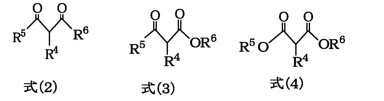
R5とR6がケイ素原子と結合していない場合は、R5とR6はそれぞれ独立して直鎖アルキル基、アリール基、アラルキル基、ハロゲン化アルキル基、ハロゲン化アリール基、ハロゲン化アラルキル基、アルケニル基、又はエポキシ基、アクリロイル基、メタクリロイル基、メルカプト基、アミノ基もしくはシアノ基を有する有機基、又はそれらの組み合わせを表し、
R4、R5又はR6のいずれかが連結基としてケイ素原子と結合している基である場合は、該ケイ素原子と結合している基はそれぞれ上記で定義した基から1つの水素原子が外れた2価の基を表す。ただし、式(3)中のR6、式(4)中のR5、及び式(4)中のR6がケイ素原子と結合する場合は単結合ではなく、連結基としてケイ素原子と結合している基を表す。)で表される基を表し、
R1はそれぞれ独立してアルキル基、アリール基、アラルキル基、ハロゲン化アルキル基、ハロゲン化アリール基、ハロゲン化アラルキル基、アルケニル基、又はエポキシ基、アクリロイル基、メタクリロイル基、メルカプト基、アミノ基もしくはシアノ基を有する有機基、又はそれらの組み合わせを表す。R2はそれぞれ独立してアルコキシ基、アシルオキシ基、又はハロゲン原子を表す。aは0~2の整数を表し、bは1~3の整数を表す。〕で表される加水分解性オルガノシランを含むリソグラフィー用レジスト下層膜形成組成物、
第2観点として、加水分解性オルガノシランが式(5):


第3観点として、上記式(1)で表される加水分解性オルガノシランの加水分解縮合物、又は上記式(1)で表される加水分解性オルガノシランと式(5)で表される有機ケイ素化合物との加水分解縮合物をポリマーとして含む第1観点又は第2観点に記載の組成物、
第4観点として、上記式(1)で表される加水分解性オルガノシランが8.00~20.00のpKa値を有するものである第1観点乃至第3観点のいずれか一つに記載の組成物、
第5観点として、更に加水分解触媒として酸を含む第1観点乃至第4観点のいずれか一つに記載の組成物、
第6観点として、更に水を含む第1観点乃至第5観点のいずれか一つに記載の組成物、
第7観点として、第1観点乃至第6観点のいずれか一つに記載のレジスト下層膜形成組成物を半導体基板上に塗布し焼成することによって得られるレジスト下層膜、
第8観点として、第1観点乃至第6観点のいずれか一つに記載のレジスト下層膜形成組成物を半導体基板上に塗布し、焼成しレジスト下層膜を形成する工程、前記下層膜の上にレジスト膜形成組成物を塗布しレジスト膜を形成する工程、前記レジスト膜を露光する工程、露光後に該レジスト膜を現像しパターン化されたレジスト膜を得る工程、該パターン化されたレジスト膜に従いレジスト下層膜をエッチングしパターン化されたレジスト下層膜を得る工程、及び該パターン化されたレジスト膜とパターン化されたレジスト下層膜に従い半導体基板を加工する工程を含む半導体装置の製造方法、及び
第9観点として、半導体基板上に有機下層膜を形成する工程、その上に第1観点乃至第6観点のいずれか一つに記載のレジスト下層膜形成組成物を塗布し焼成しレジスト下層膜を形成する工程、前記レジスト下層膜の上にレジスト膜形成組成物を塗布しレジスト膜を形成する工程、前記レジスト膜を露光する工程、露光後に該レジスト膜を現像しパターン化されたレジスト膜を得る工程、該パターン化されたレジスト膜に従いレジスト下層膜をエッチングしパターン化されたレジスト下層膜を得る工程、該パターン化されたレジスト下層膜に従い有機下層膜をエッチングする工程、及び該パターン化された有機下層膜に従い半導体基板を加工する工程を含む半導体装置の製造方法である。
また、本発明のレジスト下層膜形成組成物から形成されたレジスト下層膜は、反射防止膜として使用でき、レジストとのインターミキシングをおこさず、レジスト膜に比較して大きなドライエッチング速度を有するものである。
また、本発明のレジスト下層膜形成組成物から形成されたレジスト下層膜は、該下層膜を構成するポリマー中に組み込まれた有機基が特定の値の酸性度を有する構造であることにより、パターン化によって得られるレジスト膜のパターン形状を改善することができるものである。
また、本発明の製造方法によると、前記レジスト下層膜形成組成物から形成された膜をレジスト下層膜として使用することにより、半導体装置を好適に製造することができる。
本発明では基板上にレジスト下層膜を塗布法により形成するか、又は基板上の有機下層膜を介してその上にレジスト下層膜を塗布法により形成し、そのレジスト下層膜上にレジスト膜(例えば、フォトレジスト、電子線レジスト)を形成する。そして、露光と現像によりレジストパターンを形成し、そのレジストパターンを用いてレジスト下層膜をドライエッチングしてパターンの転写を行い、そのパターンにより基板を加工するか、又は有機下層膜をエッチングによりパターン転写しその有機下層膜により基板の加工を行う。
微細なパターンを形成する上で、パターン倒れを防ぐためにレジスト膜厚が薄くなる傾向がある。レジストの薄膜化によりその下層に存在する膜にパターンを転写するためのドライエッチングは、上層の膜よりもエッチング速度が高くなければパターン転写ができない。本発明では基板上に有機下層膜を介するか、又は有機下層膜を介さず、その上に本発明のレジスト下層膜(無機系シリコン系化合物含有)を被覆し、その上にレジスト膜(有機レジスト膜)の順で被覆される。有機系成分の膜と無機系成分の膜はエッチングガスの選択によりドライエッチング速度が大きく異なり、有機系成分の膜は酸素系ガスでドライエッチング速度が高くなり、無機系成分の膜はハロゲン含有ガスでドライエッチング速度が高くなる。
例えばレジストパターンが形成され、その下層に存在している本発明のレジスト下層膜をハロゲン含有ガスでドライエッチングしてレジスト下層膜にパターンを転写し、そのレジスト下層膜に転写されたパターンでハロゲン含有ガスを用いて基板加工を行う。あるいは、パターン転写されたレジスト下層膜を用いて、その下層の有機下層膜を酸素系ガスでドライエッチングして有機下層膜にパターン転写を行って、そのパターン転写された有機下層膜で、ハロゲン含有ガスを用いて基板加工を行う。
本発明では当該レジスト下層膜がハードマスクとして機能するものであり、上記式(1)の構造中のアルコキシ基やアシロキシ基、ハロゲン原子等の加水分解性基は加水分解乃至部分加水分解し、その後にシラノール基の縮合反応によりポリシロキサン構造のポリマーを形成する。このポリオルガノシロキサン構造はハードマスクとしての十分な機能を有している。
そして、ポリオルガノシロキサン構造(中間膜)は、その下に存在する有機下層膜のエッチングや、基板の加工(エッチング)にハードマスクとして有効である。即ち、基板加工時や有機下層膜の酸素系ドライエッチングガスに対して十分な耐ドライエッチング性を有するものである。
本発明のレジスト下層膜がこれらの上層レジストに対するドライエッチング速度の向上と、基板加工時等の耐ドライエッチング性を具備するものである。
本発明のレジスト下層膜形成組成物によるレジスト下層膜は、1-3ジケトン構造、そのジケトン構造の異性体であるエノール構造、1-3ケトエステル構造、1-3ジエステル構造を有するシランを含み形成される。これらは1-3ジケトンを少なくとも含む構造であり、この構造を含んでいることが必要である。これらの構造を有することにより上層に存在するレジスト膜との相乗効果によりパターン形状がフッティングになることを防ぎ、ストレートなパターン形状が得られるものである。これは1-3ジケトン構造のα位に存在する水素原子の酸性度によるものと考えられる。この様な酸性度を有することの重要性は上層にあるレジストの露光時に効果を発するものと考えられる。
この酸性度が高い(pKa値が低い)ことによってパターン形状の改善が得られる。しかし、この酸性度が高すぎるとレジスト下層膜形成組成物のゲル化を生じ好ましくない。
また、この様な少なくとも1-3ジケトン構造を有する有機基はポリマー中に組み込まれていることが必要であり、ポリマー中に組み込まれるために加水分解性シランの有機基として含まれることが好ましい。ポリマー中に組み込まれることにより、下層膜を形成する過程での焼成により焼失することを防ぐことができる。
本発明はシランとして加水分解性オルガノシラン、その加水分解物、又はその加水分解縮合物を含み、該シランが下記式(1)で表される加水分解性オルガノシランを含むリソグラフィー用レジスト下層膜形成組成物である。
シラン全体中のケイ素原子に対する式(2)で表される部分構造の割合が50モル%未満、例えば0.5~30モル%、0.5~25モル%、0.5~15モル%、又は0.5~10モル%の割合で含有することができる。
本発明のレジスト下層膜形成組成物は、式(1)で表される加水分解性オルガノシラン、その加水分解物、又はその加水分解縮合物と、溶剤とを含む。そして任意成分として酸、水、アルコール、硬化触媒、酸発生剤、他の有機ポリマー、吸光性化合物、及び界面活性剤等を含むことができる。
本発明のレジスト下層膜形成組成物における固形分は、例えば0.1~50質量%、又は0.1~30質量%、0.1~25質量%である。ここで固形分とはレジスト下層膜形成組成物の全成分から溶剤成分を除いたものである。
固形分中に占める加水分解性オルガノシラン、その加水分解物、及びその加水分解縮合物の割合は、20質量%以上であり、例えば50~100質量%、60~100質量%、70~100質量%である。
式(1)中のR3は、式(2)、式(3)、又は式(4)で表される基である。式(1)中のR1はそれぞれ独立してアルキル基、アリール基、アラルキル基、ハロゲン化アルキル基、ハロゲン化アリール基、ハロゲン化アラルキル基、アルケニル基、又はエポキシ基、アクリロイル基、メタクリロイル基、メルカプト基、アミノ基もしくはシアノ基を有する有機基、又はそれらの組み合わせを表す。R2はそれぞれ独立してアルコキシ基、アシルオキシ基、又はハロゲン原子を表す。aは0~2の整数を表し、bは1~3の整数を表す。
またこれらのフッ素、塩素、臭素、又はヨウ素等のハロゲン原子が置換した有機基が挙げられる。
アクリロイル基を有する有機基としては、アクリロイルメチル基、アクリロイルエチル基、アクリロイルプロピル基等が挙げられる。
メタクリロイル基を有する有機基としては、メタクリロイルメチル基、メタクリロイルエチル基、メタクリロイルプロピル基等が挙げられる。
メルカプト基を有する有機基としては、エチルメルカプト基、ブチルメルカプト基、ヘキシルメルカプト基、オクチルメルカプト基等が挙げられる。
シアノ基を有する有機基としては、シアノエチル基、シアノプロピル基等が挙げられる。
スルホニル基を有する有機基は、メチルスルホニル基、アリルスルホニル基、フェニルスルホニル基等が挙げられる。
上記式(1)で表される加水分解性オルガノシランはpKaが8.00~20.00、又は8.00~13.00の範囲のものを用いることができる。上記pKaが8.00以下では酸性度が高すぎ安定性が低い。また、pKaが20.00を超える場合はリソグラフィー工程で良好なレジストパターンを形成することができない。
上記式(1)で表される加水分解性オルガノシランは式(2)で表される構造として例えば以下に例示される。

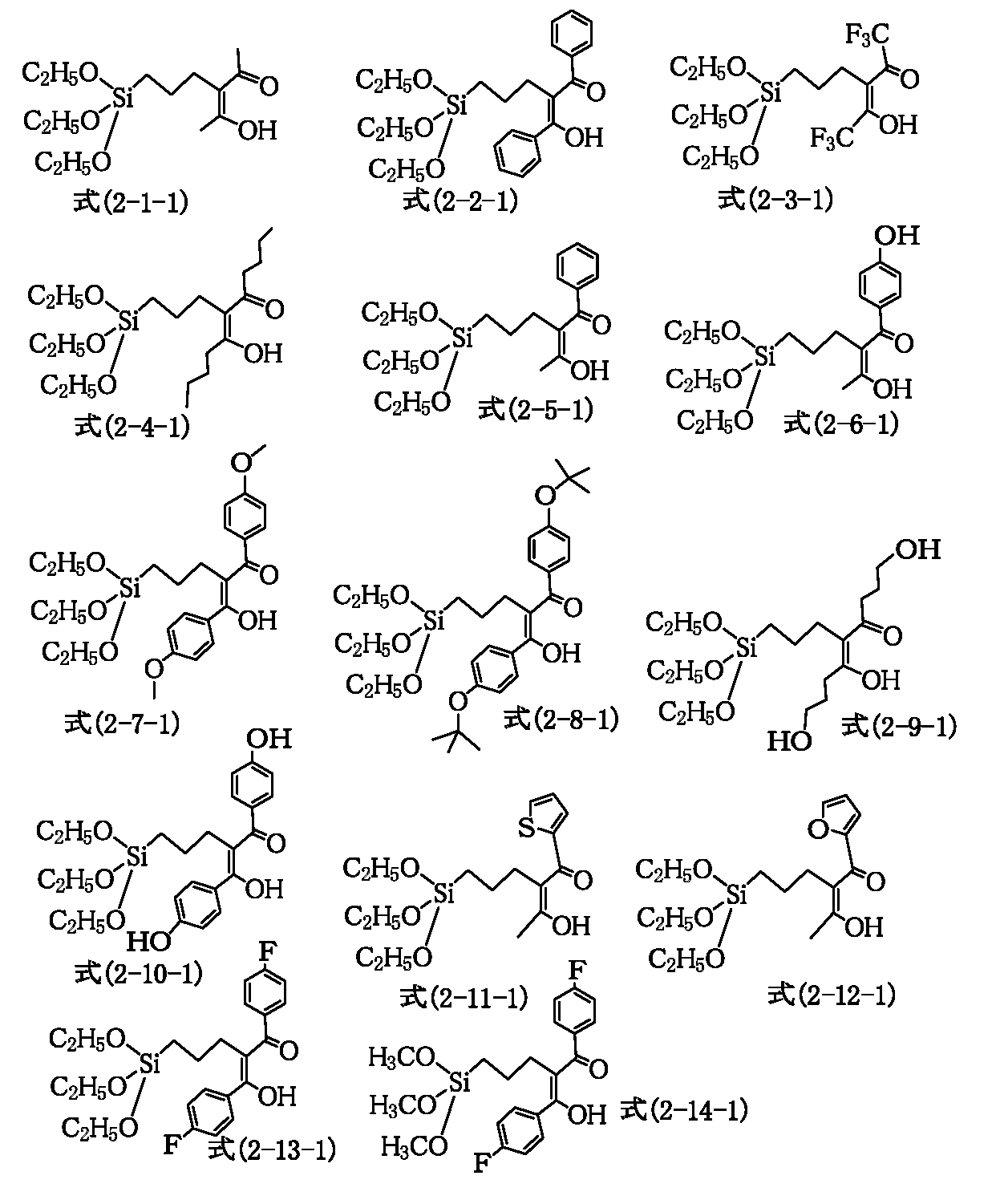
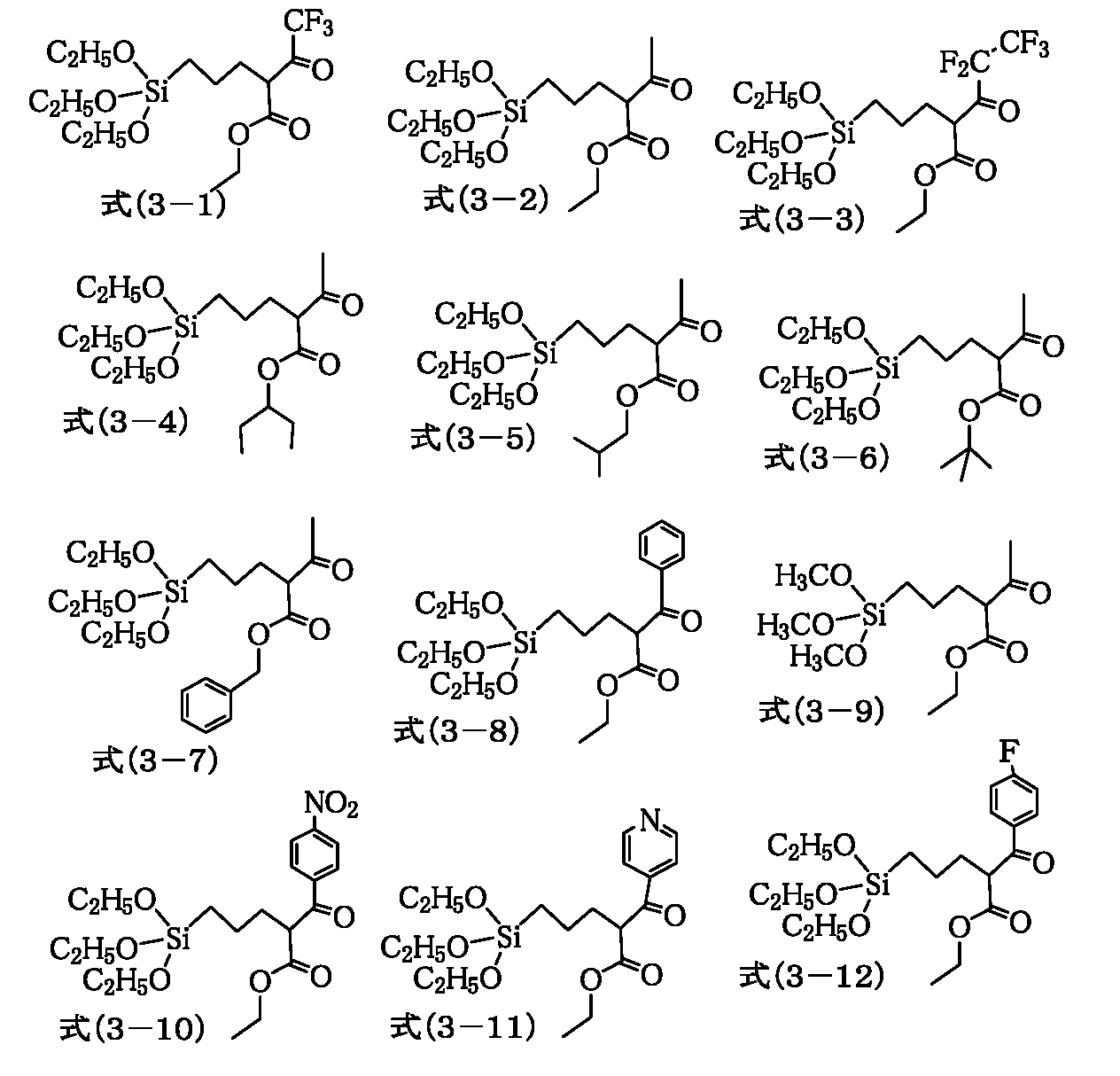

また、本発明では上記式(1)で表される加水分解性オルガノシランの加水分解縮合物、又は式(1)で表される加水分解性オルガノシランと式(5)で表される有機ケイ素化合物との加水分解縮合物を用いることができる。
本発明では式(1)で表される加水分解性オルガノシランと、式(5)で表される有機ケイ素化合物を併用して使用することができる。
すなわち、式(1)で表される加水分解性オルガノシラン、その加水分解物、又はその加水分解縮合物と、式(5)で表される有機ケイ素化合物、その加水分解物、又はその加水分解縮合物を併用して使用することができる。
これらは加水分解縮合物(ポリオルガノシロキサンのポリマー)として使用することが好ましく、式(1)で表される加水分解性オルガノシランと式(5)で表される有機ケイ素化合物との加水分解縮合物(ポリオルガノシロキサンのポリマー)を用いることが好ましい。
式(6)は、bが0を表す場合、2つのケイ素原子が単結合した有機ケイ素化合物を表し、bが1を表す場合、アルキレン基又はアリーレン基を介して2つのケイ素原子が結合した有機ケイ素化合物を表す。
上記アルキル基、アルコキシ基、アシルオキシ基、又はハロゲン原子としては式(1)に例示したものを用いることができる。またアルキレン基、アリーレン基としては上記アルキル基、及びアリール基に対応する2価の有機基を例示することができる。
式(1)で表される加水分解性オルガノシランと式(5)で表される有機ケイ素化合物との加水分解縮合物の具体例として以下に例示される。
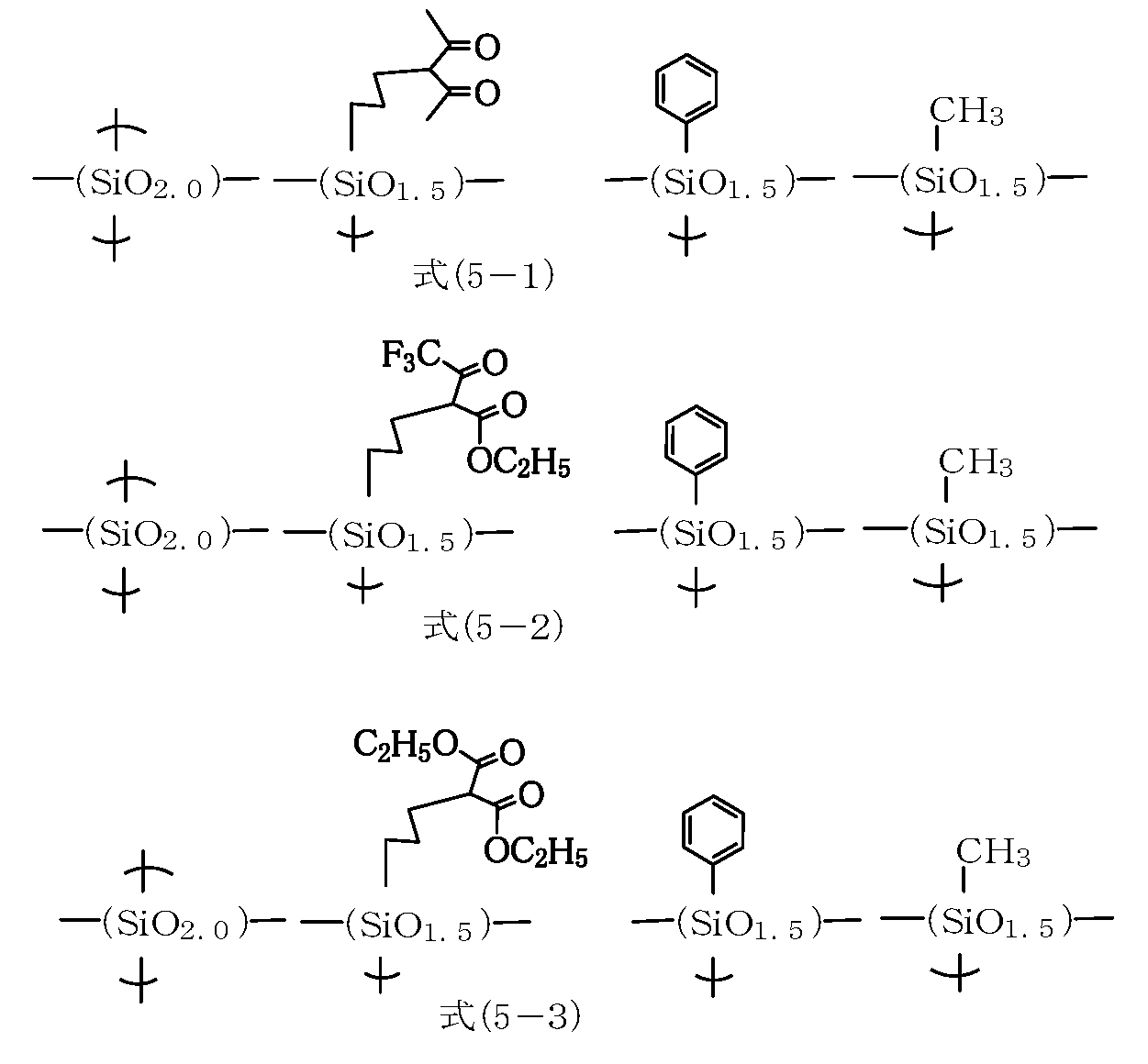
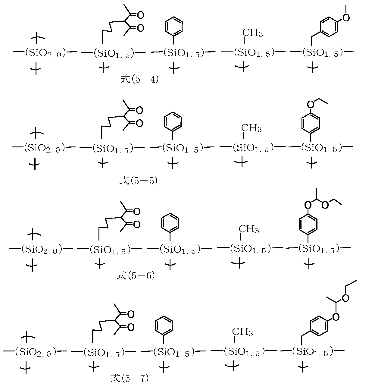
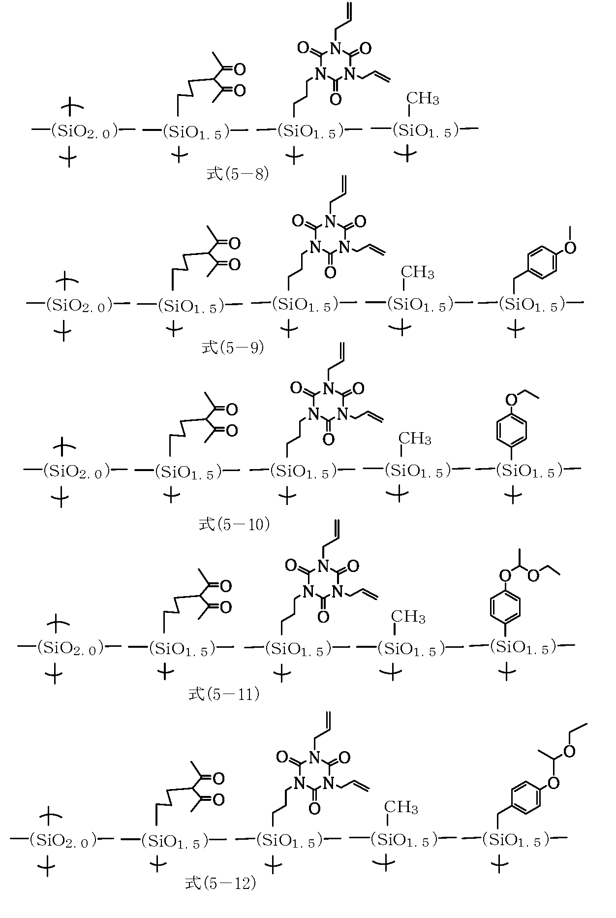
また、加水分解性基の1モル当たり0.001~10モル、好ましくは0.001~1モルの加水分解触媒を用いることができる。
加水分解は完全に加水分解を行うことも、部分加水分解することでも良い。即ち、加水分解縮合物中に加水分解物やモノマーが残存していても良い。
加水分解し縮合させる際に触媒を用いることができる。
加水分解触媒としては、金属キレート化合物、有機酸、無機酸、有機塩基、無機塩基を挙げることができる。
特に、アセトン、メチルエチルケトン、メチル-n-プロピルケトン、メチル-n-ブチルケトン、ジエチルケトン、メチル-i-ブチルケトン、メチル-n-ペンチルケトン、エチル-n-ブチルケトン、メチル-n-ヘキシルケトン、ジ-i-ブチルケトン、トリメチルノナノン、シクロヘキサノン、メチルシクロヘキサノン、2,4-ペンタンジオン、アセトニルアセトン、ジアセトンアルコール、アセトフェノン、フェンチョン(1,1,3-トリメチル-2-ノルボルネン)等のケトン系溶媒が溶液の保存安定性の点で好ましい。
硬化触媒としては、アンモニウム塩、ホスフィン類、ホスホニウム塩、スルホニウム塩を用いることができる。
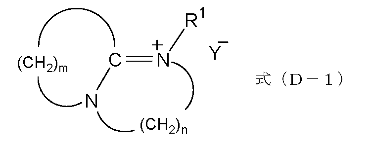

式(D-3):
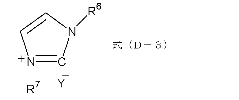
式(D-4):
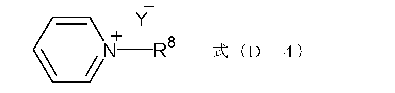
式(D-5):
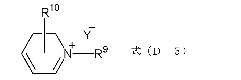
式(D-6):



加水分解性オルガノシランを溶剤中で触媒を用いて加水分解し縮合し、得られた加水分解縮合物(ポリマー)は減圧蒸留等により副生成物のアルコールや用いた加水分解触媒や水を同時に除去することができる。また、加水分解に用いた酸や塩基触媒を中和やイオン交換により取り除くことができる。そして本発明のリソグラフィー用レジスト下層膜形成組成物では、その加水分解縮合物を含むレジスト下層膜形成組成物は安定化のために有機酸、水、アルコール、又はそれらの組み合わせを添加することができる。
有機ポリマー化合物を使用することにより、本発明のリソグラフィー用下層膜形成組成物から形成されるレジスト下層膜のドライエッチング速度(単位時間当たりの膜厚の減少量)、減衰係数及び屈折率等を調整することができる。
有機ポリマー化合物としては特に制限はなく、種々の有機ポリマーを使用することができる。縮重合ポリマー及び付加重合ポリマー等を使用することができる。ポリエステル、ポリスチレン、ポリイミド、アクリルポリマー、メタクリルポリマー、ポリビニルエーテル、フェノールノボラック、ナフトールノボラック、ポリエーテル、ポリアミド、ポリカーボネート等の付加重合ポリマー及び縮重合ポリマーを使用することができる。吸光部位として機能するベンゼン環、ナフタレン環、アントラセン環、トリアジン環、キノリン環、及びキノキサリン環等の芳香環構造を有する有機ポリマーが好ましく使用される。
有機ポリマー化合物として付加重合ポリマーが使用される場合、そのポリマー化合物は単独重合体でもよく共重合体であってもよい。付加重合ポリマーの製造には付加重合性モノマーが使用される。そのような付加重合性モノマーとしてはアクリル酸、メタクリル酸、アクリル酸エステル化合物、メタクリル酸エステル化合物、アクリルアミド化合物、メタクリルアミド化合物、ビニル化合物、スチレン化合物、マレイミド化合物、マレイン酸無水物、アクリロニトリル等が挙げられる。
スチレン化合物としては、スチレン、ヒドロキシスチレン、クロロスチレン、ブロモスチレン、メトキシスチレン、シアノスチレン及びアセチルスチレン等が挙げられる。
有機ポリマー化合物としては、重量平均分子量が、例えば1000~1000000であり、または3000~300000であり、または5000~200000であり、または10000~100000であるポリマー化合物を使用することができる。
有機ポリマー化合物が使用される場合、その割合としては、縮合物(ポリオルガノシロキサン)100質量部に対して、1~200質量部、または5~100質量部、または10~50質量部、または20~30質量部である。
酸発生剤としては、熱酸発生剤や光酸発生剤が挙げられる。
光酸発生剤は、レジストの露光時に酸を生ずる。そのため、下層膜の酸性度の調整ができる。これは、下層膜の酸性度を上層のレジストとの酸性度に合わせるための一方法である。また、下層膜の酸性度の調整によって、上層に形成されるレジストのパターン形状の調整ができる。
オニウム塩化合物としてはジフェニルヨードニウムヘキサフルオロホスフエート、ジフェニルヨードニウムトリフルオロメタンスルホネート、ジフェニルヨードニウムノナフルオロノルマルブタンスルホネート、ジフェニルヨードニウムパーフルオロノルマルオクタンスルホネート、ジフェニルヨードニウムカンファースルホネート、ビス(4-tert-ブチルフェニル)ヨードニウムカンファースルホネート及びビス(4-tert-ブチルフェニル)ヨードニウムトリフルオロメタンスルホネート等のヨードニウム塩化合物、及びトリフェニルスルホニウムヘキサフルオロアンチモネート、トリフェニルスルホニウムノナフルオロノルマルブタンスルホネート、トリフェニルスルホニウムカンファースルホネート及びトリフェニルスルホニウムトリフルオロメタンスルホネート等のスルホニウム塩化合物等が挙げられる。
スルホンイミド化合物としては、例えばN-(トリフルオロメタンスルホニルオキシ)スクシンイミド、N-(ノナフルオロノルマルブタンスルホニルオキシ)スクシンイミド、N-(カンファースルホニルオキシ)スクシンイミド及びN-(トリフルオロメタンスルホニルオキシ)ナフタルイミド等が挙げられる。
ジスルホニルジアゾメタン化合物としては、例えば、ビス(トリフルオロメチルスルホニル)ジアゾメタン、ビス(シクロヘキシルスルホニル)ジアゾメタン、ビス(フェニルスルホニル)ジアゾメタン、ビス(p-トルエンスルホニル)ジアゾメタン、ビス(2,4-ジメチルベンゼンスルホニル)ジアゾメタン、及びメチルスルホニル-p-トルエンスルホニルジアゾメタン等が挙げられる。
光酸発生剤が使用される場合、その割合としては、縮合物(ポリオルガノシロキサン)100質量部に対して、0.01~5質量部、または0.1~3質量部、または0.5~1質量部である。
本発明のレジスト下層膜形成組成物に含まれる界面活性剤としては、例えば、ポリオキシエチレンラウリルエーテル、ポリオキシエチレンステアリルエーテル、ポリオキシエチレンセチルエーテル、ポリオキシエチレンオレイルエーテル等のポリオキシエチレンアルキルエーテル類、ポリオキシエチレンオクチルフエノールエーテル、ポリオキシエチレンノニルフエノールエーテル等のポリオキシエチレンアルキルアリルエーテル類、ポリオキシエチレン・ポリオキシプロピレンブロツクコポリマー類、ソルビタンモノラウレート、ソルビタンモノパルミテート、ソルビタンモノステアレート、ソルビタンモノオレエート、ソルビタントリオレエート、ソルビタントリステアレート等のソルビタン脂肪酸エステル類、ポリオキシエチレンソルビタンモノラウレート、ポリオキシエチレンソルビタンモノパルミテート、ポリオキシエチレンソルビタンモノステアレート、ポリオキシエチレンソルビタントリオレエート、ポリオキシエチレンソルビタントリステアレート等のポリオキシエチレンソルビタン脂肪酸エステル類等のノニオン系界面活性剤、商品名エフトップEF301、EF303、EF352((株)トーケムプロダクツ製)、商品名メガファックF171、F173、R-08、R-30(大日本インキ化学工業(株)製)、フロラードFC430、FC431(住友スリーエム(株)製)、商品名アサヒガードAG710,サーフロンS-382、SC101、SC102、SC103、SC104、SC105、SC106(旭硝子(株)製)等のフッ素系界面活性剤、及びオルガノシロキサンポリマ-KP341(信越化学工業(株)製)等を挙げることができる。これらの界面活性剤は単独で使用してもよいし、また二種以上の組み合わせで使用することもできる。界面活性剤が使用される場合、その割合としては、縮合物(ポリオルガノシロキサン)100質量部に対して0.0001~5質量部、または0.001~1質量部、または0.01~0.5質量部である。
半導体装置の製造に使用される基板(例えば、シリコンウエハー基板、シリコン/二酸化シリコン被覆基板、シリコンナイトライド基板、ガラス基板、ITO基板、ポリイミド基板、及び低誘電率材料(low-k材料)被覆基板等)の上に、スピナー、コーター等の適当な塗布方法により本発明のレジスト下層膜形成組成物が塗布され、その後、焼成することによりレジスト下層膜が形成される。焼成する条件としては、焼成温度80℃~250℃、焼成時間0.3~60分間の中から適宜、選択される。好ましくは、焼成温度150℃~250℃、焼成時間0.5~2分間である。ここで、形成される下層膜の膜厚としては、例えば、10~1000nmであり、または20~500nmであり、または50~300nmであり、または100~200nmである。
本発明では基板上に有機下層膜を成膜した後、この上に本発明のレジスト下層膜を成膜し、更にその上にフォトレジストを被覆することができる。これによりフォトレジストのパターン幅が狭くなり、パターン倒れを防ぐ為にフォトレジストを薄く被覆した場合でも、適切なエッチングガスを選択することにより基板の加工が可能になる。例えば、フォトレジストに対して十分に早いエッチング速度となるフッ素系ガスをエッチングガスとして本発明のレジスト下層膜に加工が可能であり、また本発明のレジスト下層膜に対して十分に早いエッチング速度となる酸素系ガスをエッチングガスとして有機下層膜の加工が可能であり、更に有機下層膜に対して十分に早いエッチング速度となるフッ素系ガスをエッチングガスとして基板の加工を行うことができる。
また、本発明ではレジストとしてフォトレジストに変えて電子線リソグラフィー用レジストを用いることができる。電子線レジストとしてはネガ型、ポジ型いずれも使用できる。酸発生剤と酸により分解してアルカリ溶解速度を変化させる基を有するバインダーからなる化学増幅型レジスト、アルカリ可溶性バインダーと酸発生剤と酸により分解してレジストのアルカリ溶解速度を変化させる低分子化合物からなる化学増幅型レジスト、酸発生剤と酸により分解してアルカリ溶解速度を変化させる基を有するバインダーと酸により分解してレジストのアルカリ溶解速度を変化させる低分子化合物からなる化学増幅型レジスト、電子線によって分解してアルカリ溶解速度を変化させる基を有するバインダーからなる非化学増幅型レジスト、電子線によって切断されアルカリ溶解速度を変化させる部位を有するバインダーからなる非化学増幅型レジストなどがある。これらの電子線レジストを用いた場合も照射源を電子線としてフォトレジストを用いた場合と同様にレジストパターンを形成することができる。
現像液としては、水酸化カリウム、水酸化ナトリウムなどのアルカリ金属水酸化物の水溶液、水酸化テトラメチルアンモニウム、水酸化テトラエチルアンモニウム、コリンなどの水酸化四級アンモニウムの水溶液、エタノールアミン、プロピルアミン、エチレンジアミンなどのアミン水溶液等のアルカリ性水溶液を例として挙げることができる。さらに、これらの現像液に界面活性剤などを加えることもできる。現像の条件としては、温度5~50℃、時間10~600秒から適宜選択される。
フッ素系ガスとしては、例えば、テトラフルオロメタン(CF4)、パーフルオロシクロブタン(C4F8)、パーフルオロプロパン(C3F8)、トリフルオロメタン、及びジフルオロメタン(CH2F2)等が挙げられる。
以下、本発明を実施例により更に具体的に説明するが、これによって本発明が限定されるものではない。
試料管:5mm、溶媒:重水素化クロロホルム、測定温度:室温、パルス間隔:5秒、積算回数:32回、基準試料:テトラメチルシラン(TMS)。
マグネチックスターラーを付けた200ml4つ口フラスコに、臭化アリルを7.70g、アセチルアセトンを19.0g(臭化アリルに対して3当量)、炭酸カリウムを17.4g(臭化アリルに対して2当量)、アセトンを61g入れ、60℃で9時間還流下に攪拌した。室温まで冷却後、アセトンを減圧留去し、酢酸エチル60gで希釈した。1N塩酸をpH3となるまで加え、有機相を純水 50gで2回洗った。有機相を濃縮・乾燥し、中間体1を7.3g得た(収率は82%)。
化合物1のpKaを計算したところ10.57であった。
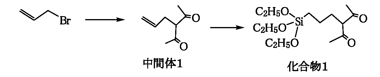
マグネチックスターラーを付けた200ml4つ口フラスコに、炭酸カリウムを9.38g(トリフルオロアセチル酢酸エチルに対して0.5当量)、アセトンを30g入れ、室温にて攪拌した。そこへ、臭化アリル8.21g(トリフルオロアセチル酢酸エチルに対して0.5当量)、トリフルオロアセチル酢酸エチル25.00gをアセトン20gに溶かした溶液を滴下した。その後、60℃で4時間還流下に攪拌した。室温まで冷却後、反応液を酢酸エチル200g、純水50gで希釈し、1N塩酸をpH3となるまで加えた。水相を除去し、さらに有機相を飽和食塩水 50gで1回洗った。有機相を濃縮乾燥し、得られた粗生成物を減圧蒸留にて精製を行い、中間体2を10.0g得た(収率は66%)。
化合物2のpKaを計算したところ8.84であった。
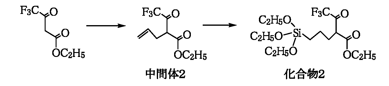
マグネチックスターラーを付けた200mlの4つ口フラスコに、アリルマロン酸ジエチルを15.00g、karstedt’s触媒(白金(0)-1,3-ジビニル-1,1,3,3-テトラメチルジシロキサン錯体の0.25M/lのキシレン溶液)を1870μl、トルエンを90g入れ、トリエトキシシラン13.7ml(アリルマロン酸ジエチルに対して1.1当量)を10分かけて滴下した。室温にて5時間攪拌後、反応液を濃縮乾燥し、得られた粗生成物を減圧蒸留にて精製を行い、化合物3を16.68g得た(収率は61%)。
化合物3のpKaを計算したところ12.97であった。
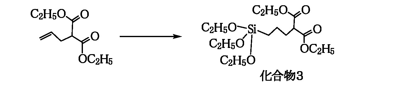
マグネチックスターラーを付けた200mlの4つ口フラスコに、アリルマロン酸ジtertブチルを19.2g、karstedt’s触媒(白金(0)-1,3-ジビニル-1,1,3,3-テトラメチルジシロキサン錯体の0.25M/lのキシレン溶液)を1870μl、トルエンを90g入れ、トリエトキシシラン13.7ml(アリルマロン酸ジtertブチルに対して1.1当量)を10分かけて滴下した。室温にて5時間攪拌後、反応液を濃縮乾燥し、得られた粗生成物を減圧蒸留にて精製を行い、化合物4を17.01g得た(収率は54%)。
1H-NMR(400MHz)inCDCl3:ケト体;0.66ppm(t、2H)、1.42~1.50ppm(m、20H)、1.93ppm(q、2H)、3.33ppm(t、1H)、3.82ppm(q、6H)、4.21ppm(q、4H)、ケト:エノールのモル比=100:0であった。
化合物4のpKaを計算したところ12.90であった。また化合物4を0.01M/lの希塩酸水溶液で加水分解してジカルボン酸に変換した誘導体のpKaは5.78であった。
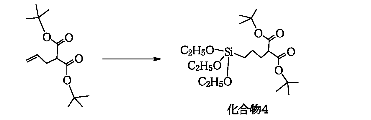
化合物(1)1.52g(全シラン中で5モル%)、テトラエトキシシラン14.58g(全シラン中で70モル%)、フェニルトリメトキシシラン0.99g(全シラン中で5モル%)、メチルトリエトキシシラン3.57g(全シラン中で20モル%)、アセトン30.99gを100mLのフラスコに入れて溶解させ、得られた混合溶液をマグネチックスターラーにて撹拌しながら加温し、還流させた。次に0.01Mの塩酸水溶液6.67gを混合溶液に添加した。240分反応させた後、得られた反応溶液を室温まで冷却した。その後、反応溶液にプロピレングリコールモノメチルエーテルアセテート21.00gを加え、反応副生物であるエタノール、水、塩酸を減圧留去し、加水分解縮合物溶液を得た。その後、加水分解縮合物溶液にプロピレングリコールジエチルエーテルを加え、最終的に、15%の加水分解縮合物溶液を得た(式(5-1)に相当)。得られたポリマーのGPCによる重量平均分子量はポリスチレン換算でMw1600であった。
化合物(2)1.94g(全シラン中で5モル%)、テトラエトキシシラン14.58g(全シラン中で70モル%)、フェニルトリメトキシシラン0.99g(全シラン中で5モル%)、メチルトリエトキシシラン3.57g(全シラン中で20モル%)、アセトン31.62gを100mLのフラスコに入れて溶解させ、得られた混合溶液をマグネチックスターラーにて撹拌しながら加温し、還流させた。次に0.01Mの塩酸水溶液6.67gを混合溶液に添加した。240分反応させた後、得られた反応溶液を室温まで冷却した。その後、反応溶液にプロピレングリコールモノメチルエーテルアセテート21.00gを加え、反応副生物であるエタノール、水、塩酸を減圧留去し、加水分解縮合物溶液を得た。その後、加水分解縮合物溶液にプロピレングリコールジエチルエーテルを加え、最終的に、15%の加水分解縮合物溶液(式(5-2)に相当)を得た。得られたポリマーのGPCによる重量平均分子量はポリスチレン換算でMw1500であった。
化合物(3)1.94g(全シラン中で5モル%)、テトラエトキシシラン14.58g(全シラン中で70モル%)、フェニルトリメトキシシラン0.99g(全シラン中で5モル%)、メチルトリエトキシシラン3.57g(全シラン中で20モル%)、アセトン31.62gを100mLのフラスコに入れて溶解させ、得られた混合溶液をマグネチックスターラーにて撹拌しながら加温し、還流させた。次に0.01Mの塩酸水溶液6.67gを混合溶液に添加した。240分反応させた後、得られた反応溶液を室温まで冷却した。その後、反応溶液にプロピレングリコールモノメチルエーテルアセテート21.00gを加え、反応副生物であるエタノール、水、塩酸を減圧留去し、加水分解縮合物溶液を得た。その後、加水分解縮合物溶液にプロピレングリコールジエチルエーテルを加え、最終的に、15%の加水分解縮合物溶液(式(5-3)に相当)を得た。得られたポリマーのGPCによる重量平均分子量はポリスチレン換算でMw1600であった。
化合物(1)1.52g(全シラン中で5モル%)、テトラエトキシシラン14.58g(全シラン中で70モル%)、フェニルトリメトキシシラン0.99g(全シラン中で5モル%)、メチルトリエトキシシラン3.30g(全シラン中で18.5モル%)、(4-メトキシベンジル)トリメトキシシラン0.36g(全シラン中で1.5モル%)、アセトン31.14g、を100mLのフラスコに入れて溶解させ、得られた混合溶液をマグネチックスターラーにて撹拌しながら加温し、還流させた。次に0.01Mの塩酸水溶液6.67gを混合溶液に添加した。240分反応させた後、得られた反応溶液を室温まで冷却した。その後、反応溶液にプロピレングリコールモノメチルエーテルアセテート21.00gを加え、反応副生物であるエタノール、水、塩酸を減圧留去し、加水分解縮合物溶液を得た。その後、加水分解縮合物溶液にプロピレングリコールジエチルエーテルを加え、最終的に、15%の加水分解縮合物溶液を得た(式(5-4)に相当)。得られたポリマーのGPCによる重量平均分子量はポリスチレン換算でMw1500であった。
化合物(1)1.52g(全シラン中で5モル%)、テトラエトキシシラン14.58g(全シラン中で70モル%)、フェニルトリメトキシシラン0.99g(全シラン中で5モル%)、メチルトリエトキシシラン3.30g(全シラン中で18.5モル%)、(4-エトキシフェニル)トリメトキシシラン0.36g(全シラン中で1.5モル%)アセトン31.14gを100mLのフラスコに入れて溶解させ、得られた混合溶液をマグネチックスターラーにて撹拌しながら加温し、還流させた。次に0.01Mの塩酸水溶液6.67gを混合溶液に添加した。240分反応させた後、得られた反応溶液を室温まで冷却した。その後、反応溶液にプロピレングリコールモノメチルエーテルアセテート21.00gを加え、反応副生物であるエタノール、水、塩酸を減圧留去し、加水分解縮合物溶液を得た。その後、加水分解縮合物溶液にプロピレングリコールジエチルエーテルを加え、最終的に、15%の加水分解縮合物溶液(式(5-5)に相当)を得た。得られたポリマーのGPCによる重量平均分子量はポリスチレン換算でMw1500であった。
化合物(1)1.52g(全シラン中で5モル%)、テトラエトキシシラン14.58g(全シラン中で70モル%)、フェニルトリメトキシシラン0.99g(全シラン中で5モル%)、メチルトリエトキシシラン3.30g(全シラン中で18.5モル%)、(4-エトキシエトキシフェニル)トリメトキシシラン0.43g(全シラン中で1.5モル%)アセトン31.24gを100mLのフラスコに入れて溶解させ、得られた混合溶液をマグネチックスターラーにて撹拌しながら加温し、還流させた。次に0.01Mの塩酸水溶液6.67gを混合溶液に添加した。240分反応させた後、得られた反応溶液を室温まで冷却した。その後、反応溶液にプロピレングリコールモノメチルエーテルアセテート21.00gを加え、反応副生物であるエタノール、水、塩酸を減圧留去し、加水分解縮合物溶液を得た。その後、加水分解縮合物溶液にプロピレングリコールジエチルエーテルを加え、最終的に、15%の加水分解縮合物溶液(式(5-6)に相当)を得た。得られたポリマーのGPCによる重量平均分子量はポリスチレン換算でMw1600であった。
化合物(1)1.52g(全シラン中で5モル%)、テトラエトキシシラン14.58g(全シラン中で70モル%)、フェニルトリメトキシシラン0.99g(全シラン中で5モル%)、メチルトリエトキシシラン3.30g(全シラン中で18.5モル%)、(4-エトキシエトキシベンジル)トリエトキシシラン0.51g(全シラン中で1.5モル%)アセトン31.36gを100mLのフラスコに入れて溶解させ、得られた混合溶液をマグネチックスターラーにて撹拌しながら加温し、還流させた。次に0.01Mの塩酸水溶液6.67gを混合溶液に添加した。240分反応させた後、得られた反応溶液を室温まで冷却した。その後、反応溶液にプロピレングリコールモノメチルエーテルアセテート21.00gを加え、反応副生物であるエタノール、水、塩酸を減圧留去し、加水分解縮合物溶液を得た。その後、加水分解縮合物溶液にプロピレングリコールジエチルエーテルを加え、最終的に、15%の加水分解縮合物溶液(式(5-7)に相当)を得た。得られたポリマーのGPCによる重量平均分子量はポリスチレン換算でMw1600であった。
化合物(1)1.52g(全シラン中で5モル%)、テトラエトキシシラン14.58g(全シラン中で70モル%)、3-(トリエトキシシリルプロピル)ジアリルイソシアヌレート2.07g(全シラン中で5モル%)、メチルトリエトキシシラン3.56g(全シラン中で20モル%)、アセトン32.61g、を100mLのフラスコに入れて溶解させ、得られた混合溶液をマグネチックスターラーにて撹拌しながら加温し、還流させた。次に0.01Mの塩酸水溶液6.67gを混合溶液に添加した。240分反応させた後、得られた反応溶液を室温まで冷却した。その後、反応溶液にプロピレングリコールモノメチルエーテルアセテート22.00gを加え、反応副生物であるエタノール、水、塩酸を減圧留去し、加水分解縮合物溶液を得た。その後、加水分解縮合物溶液にプロピレングリコールジエチルエーテルを加え、最終的に、15%の加水分解縮合物溶液を得た(式(5-8)に相当)。得られたポリマーのGPCによる重量平均分子量はポリスチレン換算でMw1600であった。
化合物(1)1.52g(全シラン中で5モル%)、テトラエトキシシラン14.58g(全シラン中で70モル%)、3-(トリエトキシシリルプロピル)ジアリルイソシアヌレート2.07g(全シラン中で5モル%)、メチルトリエトキシシラン3.30g(全シラン中で18.5モル%)、(4-メトキシベンジル)トリメトキシシラン0.36g(全シラン中で1.5モル%)、アセトン32.75g、を100mLのフラスコに入れて溶解させ、得られた混合溶液をマグネチックスターラーにて撹拌しながら加温し、還流させた。次に0.01Mの塩酸水溶液6.67gを混合溶液に添加した。240分反応させた後、得られた反応溶液を室温まで冷却した。その後、反応溶液にプロピレングリコールモノメチルエーテルアセテート22.00gを加え、反応副生物であるエタノール、水、塩酸を減圧留去し、加水分解縮合物溶液を得た。その後、加水分解縮合物溶液にプロピレングリコールジエチルエーテルを加え、最終的に、15%の加水分解縮合物溶液を得た(式(5-9)に相当)。得られたポリマーのGPCによる重量平均分子量はポリスチレン換算でMw1600であった。
化合物(1)1.52g(全シラン中で5モル%)、テトラエトキシシラン14.58g(全シラン中で70モル%)、3-(トリエトキシシリルプロピル)ジアリルイソシアヌレート2.07g(全シラン中で5モル%)、メチルトリエトキシシラン3.30g(全シラン中で18.5モル%)、(4-エトキシフェニル)トリメトキシシラン0.36g(全シラン中で1.5モル%)、アセトン32.75g、を100mLのフラスコに入れて溶解させ、得られた混合溶液をマグネチックスターラーにて撹拌しながら加温し、還流させた。次に0.01Mの塩酸水溶液6.67gを混合溶液に添加した。240分反応させた後、得られた反応溶液を室温まで冷却した。その後、反応溶液にプロピレングリコールモノメチルエーテルアセテート22.00gを加え、反応副生物であるエタノール、水、塩酸を減圧留去し、加水分解縮合物溶液を得た。その後、加水分解縮合物溶液にプロピレングリコールジエチルエーテルを加え、最終的に、15%の加水分解縮合物溶液を得た(式(5-10)に相当)。得られたポリマーのGPCによる重量平均分子量はポリスチレン換算でMw1600であった。
化合物(1)1.52g(全シラン中で5モル%)、テトラエトキシシラン14.58g(全シラン中で70モル%)、3-(トリエトキシシリルプロピル)ジアリルイソシアヌレート2.07g(全シラン中で5モル%)、メチルトリエトキシシラン3.30g(全シラン中で18.5モル%)、(4-エトキシエトキシフェニル)トリメトキシシラン0.43g(全シラン中で1.5モル%)、アセトン32.85g、を100mLのフラスコに入れて溶解させ、得られた混合溶液をマグネチックスターラーにて撹拌しながら加温し、還流させた。次に0.01Mの塩酸水溶液6.67gを混合溶液に添加した。240分反応させた後、得られた反応溶液を室温まで冷却した。その後、反応溶液にプロピレングリコールモノメチルエーテルアセテート22.00gを加え、反応副生物であるエタノール、水、塩酸を減圧留去し、加水分解縮合物溶液を得た。その後、加水分解縮合物溶液にプロピレングリコールジエチルエーテルを加え、最終的に、15%の加水分解縮合物溶液を得た(式(5-11)に相当)。得られたポリマーのGPCによる重量平均分子量はポリスチレン換算でMw1600であった。
化合物(1)1.52g(全シラン中で5モル%)、テトラエトキシシラン14.58g(全シラン中で70モル%)、3-(トリエトキシシリルプロピル)ジアリルイソシアヌレート2.07g(全シラン中で5モル%)、メチルトリエトキシシラン3.30g(全シラン中で18.5モル%)、(4-エトキシエトキシベンジル)トリメトキシシラン0.51g(全シラン中で1.5モル%)、アセトン32.98g、を100mLのフラスコに入れて溶解させ、得られた混合溶液をマグネチックスターラーにて撹拌しながら加温し、還流させた。次に0.01Mの塩酸水溶液6.67gを混合溶液に添加した。240分反応させた後、得られた反応溶液を室温まで冷却した。その後、反応溶液にプロピレングリコールモノメチルエーテルアセテート22.00gを加え、反応副生物であるエタノール、水、塩酸を減圧留去し、加水分解縮合物溶液を得た。その後、加水分解縮合物溶液にプロピレングリコールジエチルエーテルを加え、最終的に、15%の加水分解縮合物溶液を得た(式(5-12)に相当)。得られたポリマーのGPCによる重量平均分子量はポリスチレン換算でMw1500であった。
テトラエトキシシラン14.58g(全シラン中で70モル%)、フェニルトリメトキシシラン0.99g(全シラン中で5モル%)、メチルトリエトキシシラン4.46g(全シラン中で25モル%)、アセトン30.05gを100mLのフラスコに入れて溶解させ、得られた混合溶液をマグネチックスターラーにて撹拌しながら加温し、還流させた。次に0.01Mの塩酸水溶液6.68gを混合溶液に添加した。240分反応させた後、得られた反応溶液を室温まで冷却した。その後、反応溶液にプロピレングリコールモノメチルエーテルアセテート20.00gを加え、反応副生物であるエタノール、水、塩酸を減圧留去し、加水分解縮合物溶液を得た。その後、加水分解縮合物溶液にプロピレングリコールジエチルエーテルを加え、最終的に、15%の加水分解縮合物溶液を得た(式(6-1)に相当)。得られたポリマーのGPCによる重量平均分子量はポリスチレン換算でMw1600であった。
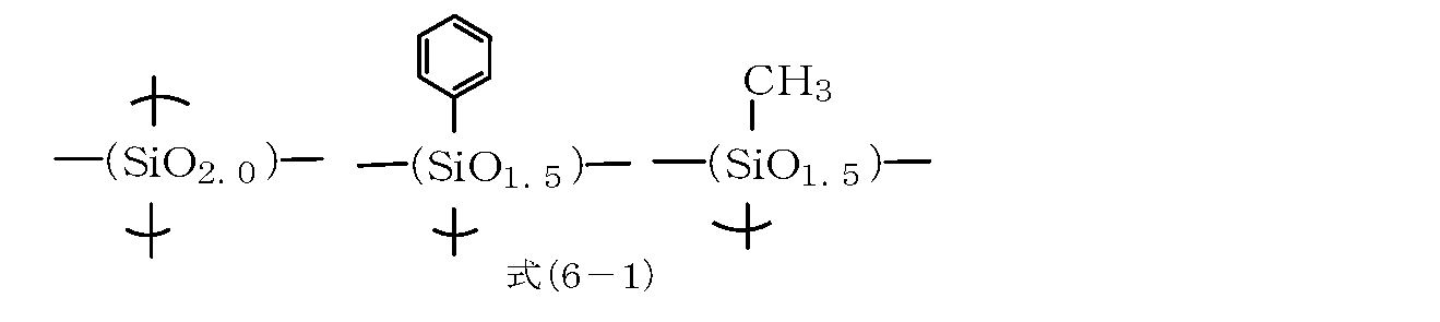
化合物(4)2.10g(全シラン中で5モル%)、テトラエトキシシラン14.58g(全シラン中で70モル%)、フェニルトリメトキシシラン0.99g(全シラン中で5モル%)、メチルトリエトキシシラン3.57g(全シラン中で20モル%)、アセトン31.86gを100mLのフラスコに入れて溶解させ、得られた混合溶液をマグネチックスターラーにて撹拌しながら加温し、還流させた。次に0.01Mの塩酸水溶液6.67gを混合溶液に添加した。240分反応させた後、得られた反応溶液を室温まで冷却した。その後、反応溶液にプロピレングリコールモノメチルエーテルアセテート21.00gを加え、反応副生物であるエタノール、水、塩酸を減圧留去し、加水分解縮合物溶液を得た。その後、加水分解縮合物溶液にプロピレングリコールジエチルエーテルを加え、最終的に、15%の加水分解縮合物溶液を得た(式(6-2)に相当)。得られたポリマーのGPCによる重量平均分子量はポリスチレン換算でMw2100であった。

上記合成例1~12及び比較合成例1~2で得られたケイ素含有ポリマー、酸、硬化触媒、添加剤、溶媒、水を表1に示す割合で混合し、0.1μmのフッ素樹脂製のフィルターで濾過することによって、レジスト下層膜形成用組成物の溶液をそれぞれ調製した。
表1中でマレイン酸はMA、ベンジルトリエチルアンモニウムクロリドはBTEAC、N-(3-トリエトキシシリプロピル)-4,5-ジヒドロイミダゾールはIMTEOS、マレイン酸モノトリフェニルスルフォニウムはTPSMA、アセチルアセトンはAcAc、トリフルオロアセト酢酸エチルはTfAcEt、マロン酸ジエチルはMADE、プロピレングリコールモノメチルエーテルアセテートはPGMEA、プロピレングリコールモノメチルエーテルはPGME、プロピレングリコールモノエチルエーテルはPGEEと略した。水は超純水を用いた。各添加量は質量部で示した。ポリマーの添加量はポリマー溶液の質量ではなく、ポリマーの質量である。
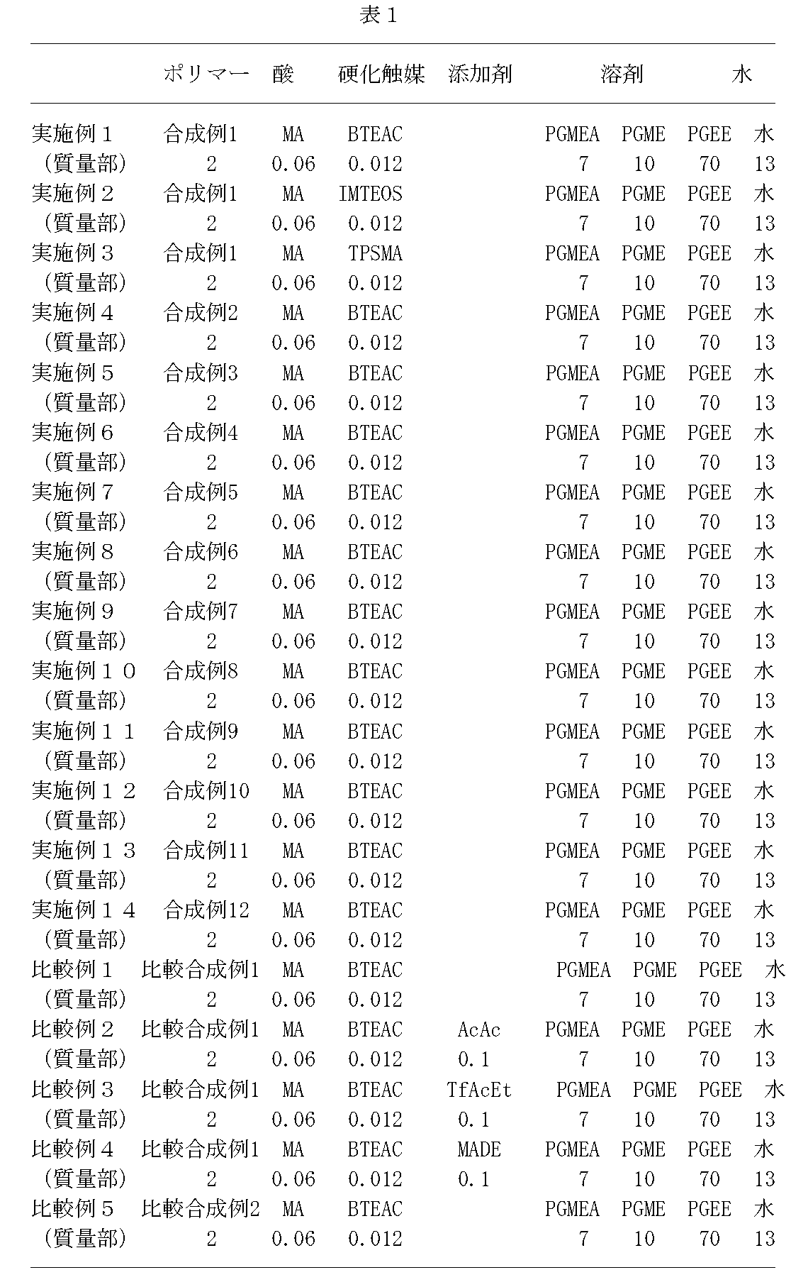
シリコンウェハー上にレジスト下層膜形成組成物をスピンコート法にて塗布し、140℃のホットプレート上で1分間焼成させレジスト下層膜を形成した。その後、上塗りレジスト組成物の溶剤に用いられるプロピレングリコールモノメチルエーテルアセテートに一分間浸漬し、浸漬の前後でのレジスト下層膜の膜厚の変化が1nm以下である場合、「良好」と判断し、表2に「○」を示した。

レジスト下層膜形成組成物をスピナーを用い、シリコンウェハー上に塗布した。ホットプレート上で240℃1分間加熱し、レジスト下層膜(膜厚0.09μm)を形成した。そして、これらのレジスト下層膜を分光エリプソメーター(J.A. Woollam社製、VUV-VASE VU-302)を用い、波長193nmでの屈折率(n値)及び光学吸光係数(k値、減衰係数とも呼ぶ)を測定した。結果を表3に示す。
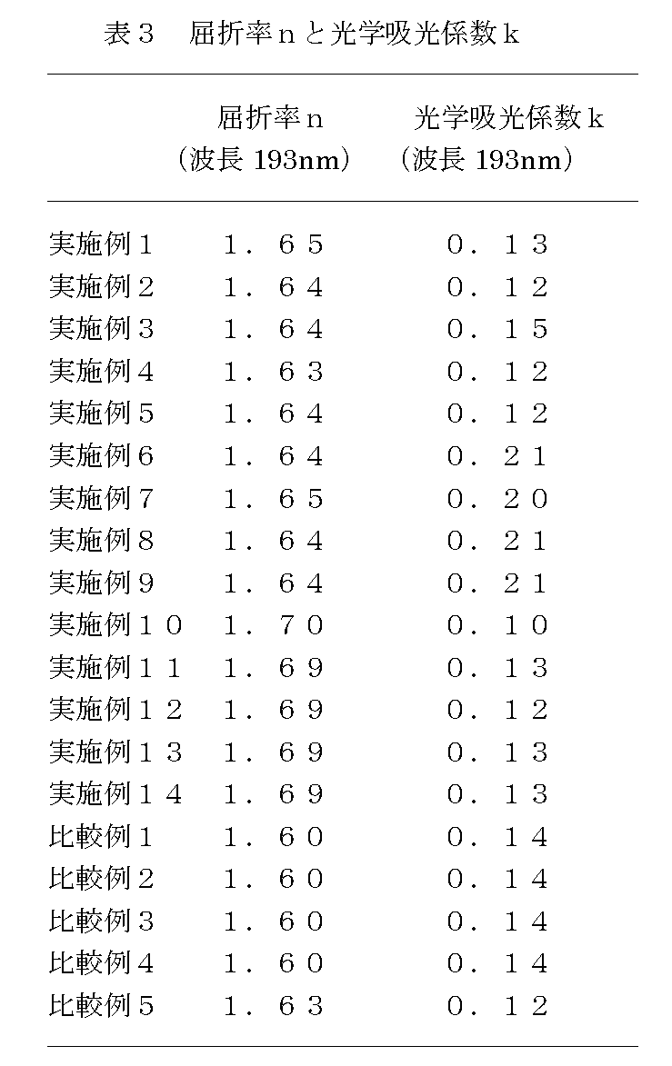
ドライエッチング速度の測定に用いたエッチャー及びエッチングガスは以下のものを用いた。
エッチャーはES401(商品名、日本サイエンティフィック製)を用い、CF4ガスでエッチングを行った。
エッチャーはRIE-10NR(商品名、サムコ製)を用い、O2ガスでエッチングを行った。
また、同様にフォトレジスト溶液(シプレー社製・商品名UV113)をスピナーを用い、シリコンウェハー上にそれぞれ0.20μmと0.04μmのレジスト膜を形成した。エッチングガスとしてCF4ガスおよびO2ガスを使用してドライエッチング速度を測定した。そしてレジスト下層膜とレジスト膜とのドライエッチング速度の比較を行った。結果を表4に示す。速度比は(レジスト下層膜)/(レジスト)のドライエッチング速度比である。
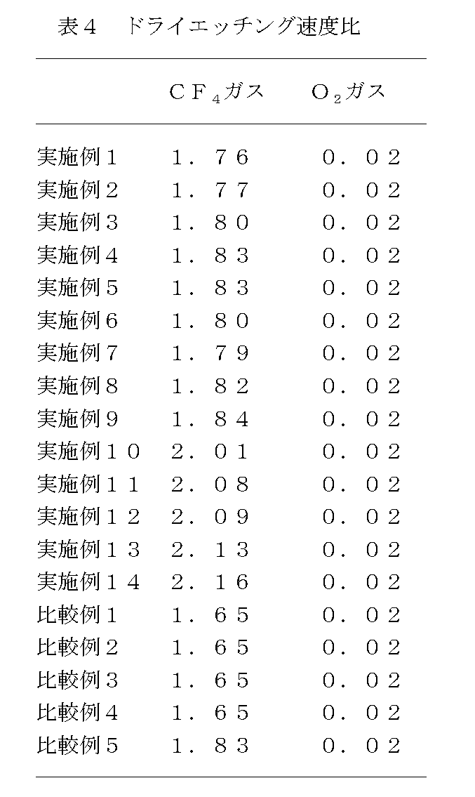
200mLのフラスコにアセナフチレンを16.5g、4-ヒドロキシスチレンを1.5g、溶媒として1,2-ジクロロエタンを60g添加した。重合開始剤としてトリフルオロホウ素を1g加え、60℃まで昇温後、24時間反応させた。この溶液にメタノール1L、水500gを加え再沈殿精製を行い、得られた白色個体をろ過後、乾燥し、白色重合体11gを得た。
得られたポリマー(式(7-1)に相当)を13C、1H-NMRおよびGPC測定したところ、アセナフチレン:4-ヒドロキシスチレン=86:14であった。Mw:6000、Mw/Mn=1.5であった。
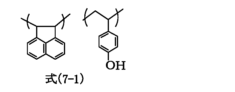
上記のポリマー(式(7-1))を含む有機下層膜(A層)形成組成物をシリコンウェハー上に塗布し、ホットプレート上で240℃で1分間加熱し、膜厚250nmの有機下層膜(A層)を得た。その上に、実施例1~実施例14および比較例1~実施例5で得られたSi含有レジスト下層膜(B層)組成物をそれぞれ塗布し、ホットプレート上で240℃で1分間加熱し、膜厚40nmのSi含有レジスト下層膜(B層)を得た。その上に市販のフォトレジスト溶液(住友化学工業(株)製、商品名PAR855)をスピナーによりそれぞれ塗布し、ホットプレート上で100℃にて1分間加熱し、膜厚150nmのフォトレジスト膜(C層)を形成した。レジストのパターニングはASML社製液浸露光機TWINSCAN XT:1900Giスキャナー(波長193nm、NA、σ: 1.20、0.94/0.74(C-quad)液浸液:水)を用いて行った。ターゲットは現像後にフォトレジストのライン幅およびそのライン間の幅が0.05μmである、いわゆるラインアンドスペース(デンスライン)であり、ライン本数が15本形成されるように設定されたマスクを通して露光を行った。その後、ホットプレート上105℃で60秒間ベークし、冷却後、工業規格の60秒シングルパドル式工程にて2.38%テトラメチルアンモニウムヒドロキシド現像液で現像した。
レジスト下層膜形成組成物を23℃2ヶ月間保存し、再度、塗布膜厚測定およびリソグラフィー評価を行った。
23℃2ヶ月保存後の塗布膜厚変化がない場合は○で示し、変化があった場合はその変化量を示した。
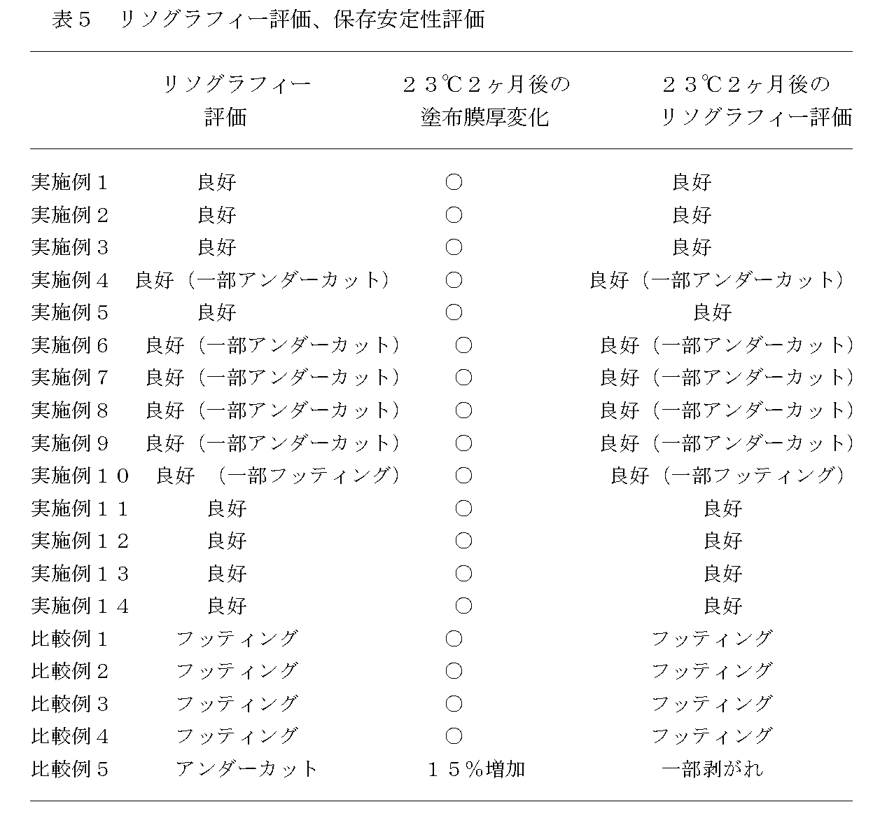
Claims (9)
- シランとして加水分解性オルガノシラン、その加水分解物、又はその加水分解縮合物を含み、該シランが下記式(1):

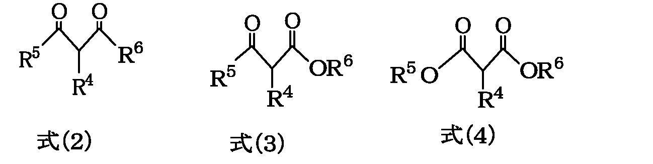
R5とR6がケイ素原子と結合していない場合は、R5とR6はそれぞれ独立して直鎖アルキル基、アリール基、アラルキル基、ハロゲン化アルキル基、ハロゲン化アリール基、ハロゲン化アラルキル基、アルケニル基、又はエポキシ基、アクリロイル基、メタクリロイル基、メルカプト基、アミノ基もしくはシアノ基を有する有機基、又はそれらの組み合わせを表し、
R4、R5又はR6のいずれかが連結基としてケイ素原子と結合している基である場合は、該ケイ素原子と結合している基はそれぞれ上記で定義した基から1つの水素原子が外れた2価の基を表す。ただし、式(3)中のR6、式(4)中のR5、及び式(4)中のR6がケイ素原子と結合する場合は単結合ではなく、連結基としてケイ素原子と結合している基を表す。)で表される基を表し、
R1はそれぞれ独立してアルキル基、アリール基、アラルキル基、ハロゲン化アルキル基、ハロゲン化アリール基、ハロゲン化アラルキル基、アルケニル基、又はエポキシ基、アクリロイル基、メタクリロイル基、メルカプト基、アミノ基もしくはシアノ基を有する有機基、又はそれらの組み合わせを表す。R2はそれぞれ独立してアルコキシ基、アシルオキシ基、又はハロゲン原子を表す。aは0~2の整数を表し、bは1~3の整数を表す。〕で表される加水分解性オルガノシランを含むリソグラフィー用レジスト下層膜形成組成物。 - 前記加水分解性オルガノシランが式(5):


- 上記式(1)で表される加水分解性オルガノシランの加水分解縮合物、又は上記式(1)で表される加水分解性オルガノシランと式(5)で表される有機ケイ素化合物との加水分解縮合物をポリマーとして含む請求項1又は請求項2に記載の組成物。
- 上記式(1)で表される加水分解性オルガノシランが8.00~20.00のpKa値を有するものである請求項1乃至請求項3のいずれか1項に記載の組成物。
- 更に加水分解触媒として酸を含む請求項1乃至請求項4のいずれか1項に記載の組成物。
- 更に水を含む請求項1乃至請求項5のいずれか1項に記載の組成物。
- 請求項1乃至請求項6のいずれか1項に記載のレジスト下層膜形成組成物を半導体基板上に塗布し焼成することによって得られるレジスト下層膜。
- 請求項1乃至請求項6のいずれか1項に記載のレジスト下層膜形成組成物を半導体基板上に塗布し、焼成しレジスト下層膜を形成する工程、前記下層膜の上にレジスト膜形成組成物を塗布しレジスト膜を形成する工程、前記レジスト膜を露光する工程、露光後に該レジスト膜を現像しパターン化されたレジスト膜を得る工程、該パターン化されたレジスト膜に従いレジスト下層膜をエッチングしパターン化されたレジスト下層膜を得る工程、及び該パターン化されたレジスト膜とパターン化されたレジスト下層膜に従い半導体基板を加工する工程を含む半導体装置の製造方法。
- 半導体基板上に有機下層膜を形成する工程、その上に請求項1乃至請求項6のいずれか1項に記載のレジスト下層膜形成組成物を塗布し焼成しレジスト下層膜を形成する工程、前記レジスト下層膜の上にレジスト膜形成組成物を塗布しレジスト膜を形成する工程、前記レジスト膜を露光する工程、露光後に該レジスト膜を現像しパターン化されたレジスト膜を得る工程、該パターン化されたレジスト膜に従いレジスト下層膜をエッチングしパターン化されたレジスト下層膜を得る工程、該パターン化されたレジスト下層膜に従い有機下層膜をエッチングする工程、及び該パターン化された有機下層膜に従い半導体基板を加工する工程を含む半導体装置の製造方法。
Priority Applications (6)
| Application Number | Priority Date | Filing Date | Title |
|---|---|---|---|
| JP2012554798A JP5818026B2 (ja) | 2011-01-24 | 2012-01-24 | ジケトン構造含有有機基を含むシリコン含有レジスト下層膜形成組成物 |
| KR1020137017718A KR101921513B1 (ko) | 2011-01-24 | 2012-01-24 | 디케톤 구조 함유 유기기를 포함하는 실리콘 함유 레지스트 하층막 형성 조성물 |
| CN201280006068.XA CN103339569B (zh) | 2011-01-24 | 2012-01-24 | 包含含有二酮结构的有机基团的含有硅的形成抗蚀剂下层膜的组合物 |
| EP12739813.9A EP2669737A1 (en) | 2011-01-24 | 2012-01-24 | Composition for forming resist underlayer films, containing silicon that bears diketone-structure-containing organic group |
| SG2013056361A SG192113A1 (en) | 2011-01-24 | 2012-01-24 | Composition for forming resist underlayer film, containing silicon that bears diketone-structure-containing organic group |
| US13/981,142 US9291900B2 (en) | 2011-01-24 | 2012-01-24 | Composition for forming resist underlayer film, containing silicon that bears diketone-structure-containing organic group |
Applications Claiming Priority (2)
| Application Number | Priority Date | Filing Date | Title |
|---|---|---|---|
| JP2011012338 | 2011-01-24 | ||
| JP2011-012338 | 2011-01-24 |
Publications (1)
| Publication Number | Publication Date |
|---|---|
| WO2012102261A1 true WO2012102261A1 (ja) | 2012-08-02 |
Family
ID=46580827
Family Applications (1)
| Application Number | Title | Priority Date | Filing Date |
|---|---|---|---|
| PCT/JP2012/051419 Ceased WO2012102261A1 (ja) | 2011-01-24 | 2012-01-24 | ジケトン構造含有有機基を含むシリコン含有レジスト下層膜形成組成物 |
Country Status (8)
| Country | Link |
|---|---|
| US (1) | US9291900B2 (ja) |
| EP (1) | EP2669737A1 (ja) |
| JP (1) | JP5818026B2 (ja) |
| KR (1) | KR101921513B1 (ja) |
| CN (1) | CN103339569B (ja) |
| SG (1) | SG192113A1 (ja) |
| TW (1) | TWI596436B (ja) |
| WO (1) | WO2012102261A1 (ja) |
Cited By (3)
| Publication number | Priority date | Publication date | Assignee | Title |
|---|---|---|---|---|
| CN104737076A (zh) * | 2012-10-31 | 2015-06-24 | 日产化学工业株式会社 | 具有酯基的含硅抗蚀剂下层膜形成用组合物 |
| WO2016080217A1 (ja) * | 2014-11-19 | 2016-05-26 | 日産化学工業株式会社 | 湿式除去が可能なシリコン含有レジスト下層膜形成組成物 |
| WO2021166567A1 (ja) * | 2020-02-19 | 2021-08-26 | Jsr株式会社 | ケイ素含有組成物及び半導体基板の製造方法 |
Families Citing this family (6)
| Publication number | Priority date | Publication date | Assignee | Title |
|---|---|---|---|---|
| WO2016121686A1 (ja) * | 2015-01-30 | 2016-08-04 | 日産化学工業株式会社 | カーボネート骨格を有する加水分解性シランを含むリソグラフィー用レジスト下層膜形成組成物 |
| US9810990B2 (en) * | 2015-03-16 | 2017-11-07 | Taiwan Semiconductor Manufacturing Company, Ltd. | Chemical treatment for lithography improvement in a negative tone development process |
| JPWO2016190261A1 (ja) * | 2015-05-25 | 2018-03-08 | 日産化学工業株式会社 | レジストパターン塗布用組成物 |
| JP2018053283A (ja) * | 2016-09-27 | 2018-04-05 | セイコーエプソン株式会社 | パターン形成方法、装飾品の製造方法、腕時計用ベルトの製造方法、配線実装構造の製造方法、半導体装置の製造方法、および、プリント配線基板の製造方法 |
| JP7373470B2 (ja) | 2019-09-19 | 2023-11-02 | 信越化学工業株式会社 | ケイ素含有レジスト下層膜形成用組成物及びパターン形成方法 |
| JP2023045109A (ja) * | 2021-09-21 | 2023-04-03 | キオクシア株式会社 | 組成物、パターン形成方法及び半導体装置 |
Citations (5)
| Publication number | Priority date | Publication date | Assignee | Title |
|---|---|---|---|---|
| JPH08300544A (ja) * | 1995-05-12 | 1996-11-19 | Nippon Synthetic Chem Ind Co Ltd:The | 積層体 |
| JPH11258813A (ja) | 1998-03-13 | 1999-09-24 | Jsr Corp | 反射防止膜形成用組成物および反射防止膜 |
| JP2000302932A (ja) * | 1999-04-21 | 2000-10-31 | Nippon Synthetic Chem Ind Co Ltd:The | 樹脂組成物及びその用途 |
| JP2004115817A (ja) * | 2003-12-04 | 2004-04-15 | Nippon Synthetic Chem Ind Co Ltd:The | 粘着剤組成物 |
| JP2007226170A (ja) | 2006-01-27 | 2007-09-06 | Shin Etsu Chem Co Ltd | 反射防止膜材料、反射防止膜を有する基板及びパターン形成方法 |
Family Cites Families (5)
| Publication number | Priority date | Publication date | Assignee | Title |
|---|---|---|---|---|
| JP2000039292A (ja) * | 1998-07-22 | 2000-02-08 | Showa Alum Corp | アルミニウム系金属製熱交換器の防錆・防食表面処理方法 |
| JP5062420B2 (ja) * | 2005-05-24 | 2012-10-31 | 日産化学工業株式会社 | ポリシラン化合物を含むリソグラフィー用下層膜形成組成物 |
| EP2196854B1 (en) * | 2007-09-11 | 2013-11-06 | Nissan Chemical Industries, Ltd. | Composition containing polymer having nitrogenous silyl group for forming resist underlayer film |
| KR101524712B1 (ko) * | 2007-11-30 | 2015-06-01 | 닛산 가가쿠 고교 가부시키 가이샤 | 블록화 이소시아네이트기를 갖는 실리콘 함유 레지스트 하층막 형성 조성물 |
| KR101579266B1 (ko) * | 2008-01-11 | 2016-01-04 | 닛산 가가쿠 고교 가부시키 가이샤 | 우레아기를 가지는 실리콘 함유 레지스트 하층막 형성 조성물 |
-
2012
- 2012-01-24 US US13/981,142 patent/US9291900B2/en active Active
- 2012-01-24 SG SG2013056361A patent/SG192113A1/en unknown
- 2012-01-24 JP JP2012554798A patent/JP5818026B2/ja active Active
- 2012-01-24 EP EP12739813.9A patent/EP2669737A1/en not_active Withdrawn
- 2012-01-24 CN CN201280006068.XA patent/CN103339569B/zh active Active
- 2012-01-24 WO PCT/JP2012/051419 patent/WO2012102261A1/ja not_active Ceased
- 2012-01-24 KR KR1020137017718A patent/KR101921513B1/ko active Active
- 2012-01-30 TW TW101102878A patent/TWI596436B/zh active
Patent Citations (5)
| Publication number | Priority date | Publication date | Assignee | Title |
|---|---|---|---|---|
| JPH08300544A (ja) * | 1995-05-12 | 1996-11-19 | Nippon Synthetic Chem Ind Co Ltd:The | 積層体 |
| JPH11258813A (ja) | 1998-03-13 | 1999-09-24 | Jsr Corp | 反射防止膜形成用組成物および反射防止膜 |
| JP2000302932A (ja) * | 1999-04-21 | 2000-10-31 | Nippon Synthetic Chem Ind Co Ltd:The | 樹脂組成物及びその用途 |
| JP2004115817A (ja) * | 2003-12-04 | 2004-04-15 | Nippon Synthetic Chem Ind Co Ltd:The | 粘着剤組成物 |
| JP2007226170A (ja) | 2006-01-27 | 2007-09-06 | Shin Etsu Chem Co Ltd | 反射防止膜材料、反射防止膜を有する基板及びパターン形成方法 |
Non-Patent Citations (3)
| Title |
|---|
| PROC. SPIE, vol. 3999, 2000, pages 330 - 334 |
| PROC. SPIE, vol. 3999, 2000, pages 357 - 364 |
| PROC. SPIE, vol. 3999, 2000, pages 365 - 374 |
Cited By (10)
| Publication number | Priority date | Publication date | Assignee | Title |
|---|---|---|---|---|
| CN104737076A (zh) * | 2012-10-31 | 2015-06-24 | 日产化学工业株式会社 | 具有酯基的含硅抗蚀剂下层膜形成用组合物 |
| US10372039B2 (en) * | 2012-10-31 | 2019-08-06 | Nissan Chemical Industries, Ltd. | Resist underlayer film forming composition containing silicon having ester group |
| WO2016080217A1 (ja) * | 2014-11-19 | 2016-05-26 | 日産化学工業株式会社 | 湿式除去が可能なシリコン含有レジスト下層膜形成組成物 |
| JPWO2016080217A1 (ja) * | 2014-11-19 | 2017-08-31 | 日産化学工業株式会社 | 湿式除去が可能なシリコン含有レジスト下層膜形成組成物 |
| US20170371242A1 (en) * | 2014-11-19 | 2017-12-28 | Nissan Chemical Industries, Ltd. | Composition for forming silicon-containing resist underlayer film removable by wet process |
| US11815815B2 (en) | 2014-11-19 | 2023-11-14 | Nissan Chemical Industries, Ltd. | Composition for forming silicon-containing resist underlayer film removable by wet process |
| WO2021166567A1 (ja) * | 2020-02-19 | 2021-08-26 | Jsr株式会社 | ケイ素含有組成物及び半導体基板の製造方法 |
| JPWO2021166567A1 (ja) * | 2020-02-19 | 2021-08-26 | ||
| JP7688012B2 (ja) | 2020-02-19 | 2025-06-03 | Jsr株式会社 | ケイ素含有組成物及び半導体基板の製造方法 |
| US12353133B2 (en) | 2020-02-19 | 2025-07-08 | Jsr Corporation | Silicon-containing composition and method of producing semiconductor substrate |
Also Published As
| Publication number | Publication date |
|---|---|
| TWI596436B (zh) | 2017-08-21 |
| CN103339569B (zh) | 2018-12-07 |
| JP5818026B2 (ja) | 2015-11-18 |
| EP2669737A1 (en) | 2013-12-04 |
| JPWO2012102261A1 (ja) | 2014-06-30 |
| KR20140006822A (ko) | 2014-01-16 |
| CN103339569A (zh) | 2013-10-02 |
| SG192113A1 (en) | 2013-08-30 |
| US20130302991A1 (en) | 2013-11-14 |
| KR101921513B1 (ko) | 2018-11-26 |
| TW201245888A (en) | 2012-11-16 |
| US9291900B2 (en) | 2016-03-22 |
Similar Documents
| Publication | Publication Date | Title |
|---|---|---|
| JP5534250B2 (ja) | スルホンアミド基を有するシリコン含有レジスト下層膜形成組成物 | |
| JP5768991B2 (ja) | 新規なシリルイソシアヌレート化合物 | |
| JP6150088B2 (ja) | スルホン構造を有する新規シラン化合物 | |
| JP5618095B2 (ja) | スルフィド結合を有するシリコン含有レジスト下層膜形成組成物 | |
| JP6319580B2 (ja) | スルホン酸オニウム塩を含有するケイ素含有euvレジスト下層膜形成組成物 | |
| JP6597980B2 (ja) | ハロゲン化スルホニルアルキル基を有するシリコン含有レジスト下層膜形成組成物 | |
| JP6436301B2 (ja) | エステル基を有するシリコン含有レジスト下層膜形成組成物 | |
| JP5590354B2 (ja) | アミック酸を含むシリコン含有レジスト下層膜形成組成物 | |
| JP6217940B2 (ja) | 環状ジエステル基を有するシリコン含有レジスト下層膜形成組成物 | |
| JP6694162B2 (ja) | ハロゲン含有カルボン酸アミド基を有する加水分解性シランを含むリソグラフィー用レジスト下層膜形成組成物 | |
| WO2012039337A1 (ja) | 保護された脂肪族アルコールを含有する有機基を有するシリコン含有レジスト下層膜形成組成物 | |
| JPWO2016009965A1 (ja) | 脂肪族多環構造含有有機基を有するシリコン含有レジスト下層膜形成組成物 | |
| JP5818026B2 (ja) | ジケトン構造含有有機基を含むシリコン含有レジスト下層膜形成組成物 | |
| JP6754098B2 (ja) | カーボネート骨格を有する加水分解性シランを含むリソグラフィー用レジスト下層膜形成組成物 | |
| WO2016080226A1 (ja) | 架橋反応性シリコン含有膜形成組成物 | |
| JP2019135238A (ja) | フェニル基含有クロモファーを有するシラン化合物 | |
| JP7157392B2 (ja) | アルカリ性現像液可溶性シリコン含有レジスト下層膜形成組成物 |
Legal Events
| Date | Code | Title | Description |
|---|---|---|---|
| 121 | Ep: the epo has been informed by wipo that ep was designated in this application |
Ref document number: 12739813 Country of ref document: EP Kind code of ref document: A1 |
|
| ENP | Entry into the national phase |
Ref document number: 2012554798 Country of ref document: JP Kind code of ref document: A |
|
| ENP | Entry into the national phase |
Ref document number: 20137017718 Country of ref document: KR Kind code of ref document: A |
|
| WWE | Wipo information: entry into national phase |
Ref document number: 13981142 Country of ref document: US |
|
| NENP | Non-entry into the national phase |
Ref country code: DE |
|
| WWE | Wipo information: entry into national phase |
Ref document number: 2012739813 Country of ref document: EP |