WO2012105067A1 - 液晶表示用基板及び液晶表示装置 - Google Patents
液晶表示用基板及び液晶表示装置 Download PDFInfo
- Publication number
- WO2012105067A1 WO2012105067A1 PCT/JP2011/061876 JP2011061876W WO2012105067A1 WO 2012105067 A1 WO2012105067 A1 WO 2012105067A1 JP 2011061876 W JP2011061876 W JP 2011061876W WO 2012105067 A1 WO2012105067 A1 WO 2012105067A1
- Authority
- WO
- WIPO (PCT)
- Prior art keywords
- liquid crystal
- crystal display
- pattern
- display device
- electrode
- Prior art date
- Legal status (The legal status is an assumption and is not a legal conclusion. Google has not performed a legal analysis and makes no representation as to the accuracy of the status listed.)
- Ceased
Links
Images


Classifications
-
- G—PHYSICS
- G02—OPTICS
- G02F—OPTICAL DEVICES OR ARRANGEMENTS FOR THE CONTROL OF LIGHT BY MODIFICATION OF THE OPTICAL PROPERTIES OF THE MEDIA OF THE ELEMENTS INVOLVED THEREIN; NON-LINEAR OPTICS; FREQUENCY-CHANGING OF LIGHT; OPTICAL LOGIC ELEMENTS; OPTICAL ANALOGUE/DIGITAL CONVERTERS
- G02F1/00—Devices or arrangements for the control of the intensity, colour, phase, polarisation or direction of light arriving from an independent light source, e.g. switching, gating or modulating; Non-linear optics
- G02F1/01—Devices or arrangements for the control of the intensity, colour, phase, polarisation or direction of light arriving from an independent light source, e.g. switching, gating or modulating; Non-linear optics for the control of the intensity, phase, polarisation or colour
- G02F1/13—Devices or arrangements for the control of the intensity, colour, phase, polarisation or direction of light arriving from an independent light source, e.g. switching, gating or modulating; Non-linear optics for the control of the intensity, phase, polarisation or colour based on liquid crystals, e.g. single liquid crystal display cells
- G02F1/1323—Arrangements for providing a switchable viewing angle
-
- G—PHYSICS
- G02—OPTICS
- G02F—OPTICAL DEVICES OR ARRANGEMENTS FOR THE CONTROL OF LIGHT BY MODIFICATION OF THE OPTICAL PROPERTIES OF THE MEDIA OF THE ELEMENTS INVOLVED THEREIN; NON-LINEAR OPTICS; FREQUENCY-CHANGING OF LIGHT; OPTICAL LOGIC ELEMENTS; OPTICAL ANALOGUE/DIGITAL CONVERTERS
- G02F1/00—Devices or arrangements for the control of the intensity, colour, phase, polarisation or direction of light arriving from an independent light source, e.g. switching, gating or modulating; Non-linear optics
- G02F1/01—Devices or arrangements for the control of the intensity, colour, phase, polarisation or direction of light arriving from an independent light source, e.g. switching, gating or modulating; Non-linear optics for the control of the intensity, phase, polarisation or colour
- G02F1/13—Devices or arrangements for the control of the intensity, colour, phase, polarisation or direction of light arriving from an independent light source, e.g. switching, gating or modulating; Non-linear optics for the control of the intensity, phase, polarisation or colour based on liquid crystals, e.g. single liquid crystal display cells
- G02F1/133—Constructional arrangements; Operation of liquid crystal cells; Circuit arrangements
- G02F1/1333—Constructional arrangements; Manufacturing methods
- G02F1/1343—Electrodes
-
- G—PHYSICS
- G02—OPTICS
- G02F—OPTICAL DEVICES OR ARRANGEMENTS FOR THE CONTROL OF LIGHT BY MODIFICATION OF THE OPTICAL PROPERTIES OF THE MEDIA OF THE ELEMENTS INVOLVED THEREIN; NON-LINEAR OPTICS; FREQUENCY-CHANGING OF LIGHT; OPTICAL LOGIC ELEMENTS; OPTICAL ANALOGUE/DIGITAL CONVERTERS
- G02F1/00—Devices or arrangements for the control of the intensity, colour, phase, polarisation or direction of light arriving from an independent light source, e.g. switching, gating or modulating; Non-linear optics
- G02F1/01—Devices or arrangements for the control of the intensity, colour, phase, polarisation or direction of light arriving from an independent light source, e.g. switching, gating or modulating; Non-linear optics for the control of the intensity, phase, polarisation or colour
- G02F1/13—Devices or arrangements for the control of the intensity, colour, phase, polarisation or direction of light arriving from an independent light source, e.g. switching, gating or modulating; Non-linear optics for the control of the intensity, phase, polarisation or colour based on liquid crystals, e.g. single liquid crystal display cells
- G02F1/133—Constructional arrangements; Operation of liquid crystal cells; Circuit arrangements
- G02F1/1333—Constructional arrangements; Manufacturing methods
-
- G—PHYSICS
- G02—OPTICS
- G02F—OPTICAL DEVICES OR ARRANGEMENTS FOR THE CONTROL OF LIGHT BY MODIFICATION OF THE OPTICAL PROPERTIES OF THE MEDIA OF THE ELEMENTS INVOLVED THEREIN; NON-LINEAR OPTICS; FREQUENCY-CHANGING OF LIGHT; OPTICAL LOGIC ELEMENTS; OPTICAL ANALOGUE/DIGITAL CONVERTERS
- G02F1/00—Devices or arrangements for the control of the intensity, colour, phase, polarisation or direction of light arriving from an independent light source, e.g. switching, gating or modulating; Non-linear optics
- G02F1/01—Devices or arrangements for the control of the intensity, colour, phase, polarisation or direction of light arriving from an independent light source, e.g. switching, gating or modulating; Non-linear optics for the control of the intensity, phase, polarisation or colour
- G02F1/13—Devices or arrangements for the control of the intensity, colour, phase, polarisation or direction of light arriving from an independent light source, e.g. switching, gating or modulating; Non-linear optics for the control of the intensity, phase, polarisation or colour based on liquid crystals, e.g. single liquid crystal display cells
- G02F1/133—Constructional arrangements; Operation of liquid crystal cells; Circuit arrangements
- G02F1/1333—Constructional arrangements; Manufacturing methods
- G02F1/1335—Structural association of cells with optical devices, e.g. polarisers or reflectors
-
- G—PHYSICS
- G02—OPTICS
- G02F—OPTICAL DEVICES OR ARRANGEMENTS FOR THE CONTROL OF LIGHT BY MODIFICATION OF THE OPTICAL PROPERTIES OF THE MEDIA OF THE ELEMENTS INVOLVED THEREIN; NON-LINEAR OPTICS; FREQUENCY-CHANGING OF LIGHT; OPTICAL LOGIC ELEMENTS; OPTICAL ANALOGUE/DIGITAL CONVERTERS
- G02F1/00—Devices or arrangements for the control of the intensity, colour, phase, polarisation or direction of light arriving from an independent light source, e.g. switching, gating or modulating; Non-linear optics
- G02F1/01—Devices or arrangements for the control of the intensity, colour, phase, polarisation or direction of light arriving from an independent light source, e.g. switching, gating or modulating; Non-linear optics for the control of the intensity, phase, polarisation or colour
- G02F1/13—Devices or arrangements for the control of the intensity, colour, phase, polarisation or direction of light arriving from an independent light source, e.g. switching, gating or modulating; Non-linear optics for the control of the intensity, phase, polarisation or colour based on liquid crystals, e.g. single liquid crystal display cells
- G02F1/133—Constructional arrangements; Operation of liquid crystal cells; Circuit arrangements
- G02F1/1333—Constructional arrangements; Manufacturing methods
- G02F1/1335—Structural association of cells with optical devices, e.g. polarisers or reflectors
- G02F1/133509—Filters, e.g. light shielding masks
- G02F1/133512—Light shielding layers, e.g. black matrix
-
- G—PHYSICS
- G02—OPTICS
- G02F—OPTICAL DEVICES OR ARRANGEMENTS FOR THE CONTROL OF LIGHT BY MODIFICATION OF THE OPTICAL PROPERTIES OF THE MEDIA OF THE ELEMENTS INVOLVED THEREIN; NON-LINEAR OPTICS; FREQUENCY-CHANGING OF LIGHT; OPTICAL LOGIC ELEMENTS; OPTICAL ANALOGUE/DIGITAL CONVERTERS
- G02F1/00—Devices or arrangements for the control of the intensity, colour, phase, polarisation or direction of light arriving from an independent light source, e.g. switching, gating or modulating; Non-linear optics
- G02F1/01—Devices or arrangements for the control of the intensity, colour, phase, polarisation or direction of light arriving from an independent light source, e.g. switching, gating or modulating; Non-linear optics for the control of the intensity, phase, polarisation or colour
- G02F1/13—Devices or arrangements for the control of the intensity, colour, phase, polarisation or direction of light arriving from an independent light source, e.g. switching, gating or modulating; Non-linear optics for the control of the intensity, phase, polarisation or colour based on liquid crystals, e.g. single liquid crystal display cells
- G02F1/133—Constructional arrangements; Operation of liquid crystal cells; Circuit arrangements
- G02F1/1333—Constructional arrangements; Manufacturing methods
- G02F1/1337—Surface-induced orientation of the liquid crystal molecules, e.g. by alignment layers
- G02F1/133707—Structures for producing distorted electric fields, e.g. bumps, protrusions, recesses, slits in pixel electrodes
-
- G—PHYSICS
- G02—OPTICS
- G02F—OPTICAL DEVICES OR ARRANGEMENTS FOR THE CONTROL OF LIGHT BY MODIFICATION OF THE OPTICAL PROPERTIES OF THE MEDIA OF THE ELEMENTS INVOLVED THEREIN; NON-LINEAR OPTICS; FREQUENCY-CHANGING OF LIGHT; OPTICAL LOGIC ELEMENTS; OPTICAL ANALOGUE/DIGITAL CONVERTERS
- G02F1/00—Devices or arrangements for the control of the intensity, colour, phase, polarisation or direction of light arriving from an independent light source, e.g. switching, gating or modulating; Non-linear optics
- G02F1/01—Devices or arrangements for the control of the intensity, colour, phase, polarisation or direction of light arriving from an independent light source, e.g. switching, gating or modulating; Non-linear optics for the control of the intensity, phase, polarisation or colour
- G02F1/13—Devices or arrangements for the control of the intensity, colour, phase, polarisation or direction of light arriving from an independent light source, e.g. switching, gating or modulating; Non-linear optics for the control of the intensity, phase, polarisation or colour based on liquid crystals, e.g. single liquid crystal display cells
- G02F1/133—Constructional arrangements; Operation of liquid crystal cells; Circuit arrangements
- G02F1/136—Liquid crystal cells structurally associated with a semi-conducting layer or substrate, e.g. cells forming part of an integrated circuit
- G02F1/1362—Active matrix addressed cells
- G02F1/1368—Active matrix addressed cells in which the switching element is a three-electrode device
-
- G—PHYSICS
- G02—OPTICS
- G02F—OPTICAL DEVICES OR ARRANGEMENTS FOR THE CONTROL OF LIGHT BY MODIFICATION OF THE OPTICAL PROPERTIES OF THE MEDIA OF THE ELEMENTS INVOLVED THEREIN; NON-LINEAR OPTICS; FREQUENCY-CHANGING OF LIGHT; OPTICAL LOGIC ELEMENTS; OPTICAL ANALOGUE/DIGITAL CONVERTERS
- G02F1/00—Devices or arrangements for the control of the intensity, colour, phase, polarisation or direction of light arriving from an independent light source, e.g. switching, gating or modulating; Non-linear optics
- G02F1/01—Devices or arrangements for the control of the intensity, colour, phase, polarisation or direction of light arriving from an independent light source, e.g. switching, gating or modulating; Non-linear optics for the control of the intensity, phase, polarisation or colour
- G02F1/13—Devices or arrangements for the control of the intensity, colour, phase, polarisation or direction of light arriving from an independent light source, e.g. switching, gating or modulating; Non-linear optics for the control of the intensity, phase, polarisation or colour based on liquid crystals, e.g. single liquid crystal display cells
- G02F1/133—Constructional arrangements; Operation of liquid crystal cells; Circuit arrangements
- G02F1/1333—Constructional arrangements; Manufacturing methods
- G02F1/1335—Structural association of cells with optical devices, e.g. polarisers or reflectors
- G02F1/133509—Filters, e.g. light shielding masks
- G02F1/133514—Colour filters
-
- G—PHYSICS
- G02—OPTICS
- G02F—OPTICAL DEVICES OR ARRANGEMENTS FOR THE CONTROL OF LIGHT BY MODIFICATION OF THE OPTICAL PROPERTIES OF THE MEDIA OF THE ELEMENTS INVOLVED THEREIN; NON-LINEAR OPTICS; FREQUENCY-CHANGING OF LIGHT; OPTICAL LOGIC ELEMENTS; OPTICAL ANALOGUE/DIGITAL CONVERTERS
- G02F1/00—Devices or arrangements for the control of the intensity, colour, phase, polarisation or direction of light arriving from an independent light source, e.g. switching, gating or modulating; Non-linear optics
- G02F1/01—Devices or arrangements for the control of the intensity, colour, phase, polarisation or direction of light arriving from an independent light source, e.g. switching, gating or modulating; Non-linear optics for the control of the intensity, phase, polarisation or colour
- G02F1/13—Devices or arrangements for the control of the intensity, colour, phase, polarisation or direction of light arriving from an independent light source, e.g. switching, gating or modulating; Non-linear optics for the control of the intensity, phase, polarisation or colour based on liquid crystals, e.g. single liquid crystal display cells
- G02F1/133—Constructional arrangements; Operation of liquid crystal cells; Circuit arrangements
- G02F1/1333—Constructional arrangements; Manufacturing methods
- G02F1/1343—Electrodes
- G02F1/134309—Electrodes characterised by their geometrical arrangement
- G02F1/134336—Matrix
-
- G—PHYSICS
- G02—OPTICS
- G02F—OPTICAL DEVICES OR ARRANGEMENTS FOR THE CONTROL OF LIGHT BY MODIFICATION OF THE OPTICAL PROPERTIES OF THE MEDIA OF THE ELEMENTS INVOLVED THEREIN; NON-LINEAR OPTICS; FREQUENCY-CHANGING OF LIGHT; OPTICAL LOGIC ELEMENTS; OPTICAL ANALOGUE/DIGITAL CONVERTERS
- G02F1/00—Devices or arrangements for the control of the intensity, colour, phase, polarisation or direction of light arriving from an independent light source, e.g. switching, gating or modulating; Non-linear optics
- G02F1/01—Devices or arrangements for the control of the intensity, colour, phase, polarisation or direction of light arriving from an independent light source, e.g. switching, gating or modulating; Non-linear optics for the control of the intensity, phase, polarisation or colour
- G02F1/13—Devices or arrangements for the control of the intensity, colour, phase, polarisation or direction of light arriving from an independent light source, e.g. switching, gating or modulating; Non-linear optics for the control of the intensity, phase, polarisation or colour based on liquid crystals, e.g. single liquid crystal display cells
- G02F1/133—Constructional arrangements; Operation of liquid crystal cells; Circuit arrangements
- G02F1/1333—Constructional arrangements; Manufacturing methods
- G02F1/1343—Electrodes
- G02F1/134309—Electrodes characterised by their geometrical arrangement
- G02F1/134381—Hybrid switching mode, i.e. for applying an electric field with components parallel and orthogonal to the substrates
-
- G—PHYSICS
- G02—OPTICS
- G02F—OPTICAL DEVICES OR ARRANGEMENTS FOR THE CONTROL OF LIGHT BY MODIFICATION OF THE OPTICAL PROPERTIES OF THE MEDIA OF THE ELEMENTS INVOLVED THEREIN; NON-LINEAR OPTICS; FREQUENCY-CHANGING OF LIGHT; OPTICAL LOGIC ELEMENTS; OPTICAL ANALOGUE/DIGITAL CONVERTERS
- G02F1/00—Devices or arrangements for the control of the intensity, colour, phase, polarisation or direction of light arriving from an independent light source, e.g. switching, gating or modulating; Non-linear optics
- G02F1/01—Devices or arrangements for the control of the intensity, colour, phase, polarisation or direction of light arriving from an independent light source, e.g. switching, gating or modulating; Non-linear optics for the control of the intensity, phase, polarisation or colour
- G02F1/13—Devices or arrangements for the control of the intensity, colour, phase, polarisation or direction of light arriving from an independent light source, e.g. switching, gating or modulating; Non-linear optics for the control of the intensity, phase, polarisation or colour based on liquid crystals, e.g. single liquid crystal display cells
- G02F1/137—Devices or arrangements for the control of the intensity, colour, phase, polarisation or direction of light arriving from an independent light source, e.g. switching, gating or modulating; Non-linear optics for the control of the intensity, phase, polarisation or colour based on liquid crystals, e.g. single liquid crystal display cells characterised by the electro-optical or magneto-optical effect, e.g. field-induced phase transition, orientation effect, guest-host interaction or dynamic scattering
- G02F1/139—Devices or arrangements for the control of the intensity, colour, phase, polarisation or direction of light arriving from an independent light source, e.g. switching, gating or modulating; Non-linear optics for the control of the intensity, phase, polarisation or colour based on liquid crystals, e.g. single liquid crystal display cells characterised by the electro-optical or magneto-optical effect, e.g. field-induced phase transition, orientation effect, guest-host interaction or dynamic scattering based on orientation effects in which the liquid crystal remains transparent
-
- G—PHYSICS
- G02—OPTICS
- G02F—OPTICAL DEVICES OR ARRANGEMENTS FOR THE CONTROL OF LIGHT BY MODIFICATION OF THE OPTICAL PROPERTIES OF THE MEDIA OF THE ELEMENTS INVOLVED THEREIN; NON-LINEAR OPTICS; FREQUENCY-CHANGING OF LIGHT; OPTICAL LOGIC ELEMENTS; OPTICAL ANALOGUE/DIGITAL CONVERTERS
- G02F2203/00—Function characteristic
- G02F2203/64—Normally black display, i.e. the off state being black
Definitions
- Embodiments described herein relate generally to a liquid crystal display substrate and a liquid crystal display device including the liquid crystal display substrate.
- the field of view of the liquid crystal display device is narrow.
- the liquid crystal display device preferably has a wide field of view. There are roughly two types of visual field control methods.
- Patent Literature 1 Japanese Patent No. 3322197
- Patent Literature 2 Japanese Patent No. 4367206
- this first visual field control system two panels including a display panel having a liquid crystal display element for performing main display and a visual angle control panel having a liquid crystal element for viewing angle control for switching between a wide visual field and a narrow visual field.
- the viewing angle control liquid crystal element is a phase difference control element, and a wide field of view and a narrow field of view are switched based on the presence or absence of a voltage applied to the phase difference control element.
- Patent Document 2 discloses a technique for making it difficult to see the display of the liquid crystal display device by forming a checker flag pattern including a bright region and a dark region in the formation region of the viewing angle control liquid crystal element.
- a viewing angle control panel in which a viewing angle control liquid crystal element is provided, and the entire display device becomes thick and heavy, which may not be practical.
- the display device is thick and heavy, the convenience of portable personal terminals such as mobile phones and mobile PCs decreases.
- a viewing angle control pixel is newly added to one display panel including a display liquid crystal display element, or a viewing angle control is applied to a part of the display pixels formed on the display panel.
- This second visual field control method is suitable for portable display devices because it is not necessary to add a viewing angle control panel.
- Patent Document 3 Japanese Patent Laid-Open No. 2010-128126
- Patent Document 3 Japanese Patent Laid-Open No. 2010-128126
- Patent Document 3 Japanese Patent Laid-Open No. 2010-128126
- Patent Document 3 Japanese Patent Laid-Open No. 2010-128126
- Patent Document 3 Japanese Patent Laid-Open No. 2010-128126
- Patent Document 3 Japanese Patent Laid-Open No. 2010-128126
- Patent Document 3 Japanese Patent Laid-Open No. 2010-128126
- Patent Document 3 Japanese Patent Laid-Open No. 2007-65046
- Patent Document 4 Japanese Patent Laid-Open No. 2007-65046
- a first counter electrode and a second counter electrode are provided in one pixel, and different counter voltages are provided between the first counter electrode and the second counter electrode connected to the thin film transistor. Is applied, and the second counter electrode is used for viewing angle control.
- the display panel is provided with viewing angle control pixels and when a viewing angle control region in which a plurality of counter electrodes are separately formed is formed on the display panel, the effective display area decreases and the display becomes dark. There is a case.
- the viewing angle control pixel or the viewing angle control region the display content is less likely to be visually recognized by surrounding third parties.
- Patent Document 4 does not discuss VA (Vertical Alignment) liquid crystal or ECB (Electrically Changed Birefringence) liquid crystal applied to a high-contrast liquid crystal display device.
- VA Vertical Alignment
- ECB Electro Mechanical Changed Birefringence
- a liquid crystal display device such as a normal VA method or ECB method is electrically connected to a color filter substrate having a common electrode and a plurality of pixel electrodes (for example, thin film transistor (TFT) elements) that drive liquid crystal, and has a comb shape. It has a basic structure for sandwiching liquid crystal with an array substrate provided with a transparent electrode formed in a pattern. In this configuration, a driving voltage is applied between the common electrode on the color filter and the pixel electrode formed on the array substrate side, and the liquid crystal is driven.
- TFT thin film transistor
- the transparent conductive film used for the pixel electrode and the common electrode on the color filter surface is usually a conductive metal oxide thin film such as ITO (IndiumInTin Oxide), IZO (Indium Zinc Oxide), IGZO (Indium Garium Zinc Oxide). Is used.
- ITO IndiumInTin Oxide
- IZO Indium Zinc Oxide
- IGZO Indium Garium Zinc Oxide
- the liquid crystal display device may be heavy and thick by providing a viewing angle control panel including a viewing angle control liquid crystal element.
- the effective aperture ratio may be reduced by providing the display panel with viewing angle control pixels.
- Embodiments of the present invention prevent a liquid crystal display device from becoming heavy and thick, prevent a reduction in aperture ratio, and perform effective viewing angle control, and a liquid crystal display substrate
- An object of the present invention is to provide a liquid crystal display device including a substrate.
- the liquid crystal display substrate includes polygonal pixels or polygonal subpixels and a linear pattern.
- Polygonal pixels or polygonal subpixels have parallel sides facing each other in a planar shape.
- the linear pattern is provided on opposite parallel sides of the polygon pixel or polygon sub-pixel and transmits oblique light.
- the liquid crystal display device includes a liquid crystal display substrate and an array substrate.
- a liquid crystal display substrate is a polygonal pixel or polygon subpixel having parallel sides facing each other in a planar shape, and a linear pattern that transmits oblique light provided on the parallel sides facing each other of the polygon pixel or polygon subpixel. It comprises.
- the array substrate is opposed to the liquid crystal display substrate through a liquid crystal layer, and includes an active element that drives the liquid crystal of the liquid crystal layer.
- ADVANTAGE OF THE INVENTION According to this invention, it can prevent that a liquid crystal display device becomes heavy and thick in viewing angle control, can prevent that an aperture ratio falls, and can perform effective viewing angle control. .
- FIG. 1 is a partial cross-sectional view illustrating an example of a liquid crystal display device according to the first embodiment.
- FIG. 2 is a partial cross-sectional view showing an example of a liquid crystal display substrate according to the first embodiment.
- FIG. 3 is a partial plan view showing an example of the liquid crystal display substrate according to the first embodiment.
- FIG. 4 is a partial cross-sectional view showing an example of the relationship between the configuration of the liquid crystal display device according to the first embodiment and oblique light.
- FIG. 5 is a partial cross-sectional view showing a modification of the shape of the transparent pattern in the liquid crystal display device according to the first embodiment.
- FIG. 6 is a partial cross-sectional view illustrating an example of a liquid crystal display device when a driving voltage is not applied in the first embodiment.
- FIG. 7 is a partial cross-sectional view showing an example of the liquid crystal display device immediately after the drive voltage is applied.
- FIG. 8 is a partial cross-sectional view showing an example of a liquid crystal display device after a certain time has elapsed since the drive voltage was applied.
- FIG. 9 is a partial cross-sectional view showing an example of the operation of the first electrodes P1 to P3 and the second electrodes C1 to C3 when a driving voltage is not applied (initial alignment state) in the liquid crystal display device.
- FIG. 10 is a partial cross-sectional view showing an example of the action of the first electrodes P1 to P3 and the second electrodes C1 to C3 when a driving voltage is applied in the liquid crystal display device.
- FIG. 11 is a partial plan view showing a first example of the first electrode provided in the sub-pixel.
- FIG. 12 is a partial plan view showing a second example of the first electrode provided in the subpixel.
- FIG. 13 is a partial plan view showing a third example of the first electrode provided in the subpixel.
- FIG. 14 is a partial plan view showing a modified example of how subpixels are arranged.
- FIG. 15 is a plan view showing an example of the relationship between the polygonal subpixel and the first electrodes P1 to P6.
- FIG. 16 is a partial cross-sectional view showing an example of a liquid crystal display substrate according to the third embodiment.
- FIG. 17 is a cross-sectional view illustrating an example of a configuration of an edge light type liquid crystal display device.
- FIG. 18 is a partial cross-sectional view illustrating an example of a liquid crystal display device during halftone display when a driving voltage is applied.
- FIG. 19 is a partial cross-sectional view showing an example of a liquid crystal display device according to the sixth embodiment.
- FIG. 20 is a partial cross-sectional view showing a first example of a configuration for driving liquid crystal with a low voltage in the liquid crystal display device according to the seventh embodiment.
- FIG. 21 is a partial cross-sectional view showing a second example of a configuration for driving liquid crystal at a low voltage in the liquid crystal display device according to the seventh embodiment.
- FIG. 1 is a partial cross-sectional view showing an example of a liquid crystal display device according to the present embodiment.
- FIG. 1 is a cross section perpendicular to a comb tooth axis of a comb-like (for example, stripe-like) electrode.
- FIG. 1 shows the operation of the liquid crystals L1 to L14 by the liquid crystal display substrate 2 and the array substrate 3, and the oblique light 8 realized by this operation.
- the vertical alignment film, the polarizing plate, the retardation film, and the TFT are not shown.
- FIG. 2 is a partial sectional view showing an example of the liquid crystal display substrate 2 in FIG.
- FIG. 3 is a partial plan view showing an example of the liquid crystal display substrate 2 according to the present embodiment.
- the A-A ′ cross section in FIG. 3 corresponds to FIG. 1.
- the liquid crystal display device 1 is a VA system or an ECB system.
- a liquid crystal having positive dielectric anisotropy is used as the ECB liquid crystal.
- liquid crystal display substrate 2 and the array substrate 3 on which liquid crystal driving elements (active elements) such as TFTs are formed face each other.
- a liquid crystal layer 4 is sandwiched between the liquid crystal display substrate 2 and the array substrate 3.
- the planar view shape of the openings of the polygonal subpixels arranged in a matrix is, for example, a square, a rectangle, a parallelogram, or a polygon that is bent in a dogleg shape ("V" shape or boomerang type).
- a linear pattern 7 sandwiched between the linear light shielding patterns 6 of the layers is provided.
- the oblique light 8 that passes through the transparent pattern 5 is used for viewing angle control.
- the thickness of the transparent pattern 5 in the vertical direction is larger than the thickness of the light shielding pattern 6 in the vertical direction. Therefore, the transparent pattern 5 protrudes closer to the liquid crystal layer 4 than the light shielding pattern 6. Further, in the liquid crystal display substrate 2, the part where the linear pattern 7 is formed is thicker than the other part such as the part where the color filters 10 to 12 are formed.
- the liquid crystal layer 4 is a VA liquid crystal. Therefore, the liquid crystals L1 to L14 of the liquid crystal layer 4 are liquid crystals having negative dielectric anisotropy.
- the initial alignment of the liquid crystals L1 to L14 in the liquid crystal layer 4 is vertical.
- the liquid crystals L 1, L 2, L 5 to L 10, L 13, L 14 are the liquid crystal display substrate 2 and the array substrate 3. Is oriented perpendicular to the surface of the substrate.
- a vertical alignment film is used, and alignment processing such as photo alignment and rubbing can be omitted.
- strict pretilt angle control such as 89 degrees required in the conventional VA method is unnecessary, and a liquid crystal with a simple initial vertical alignment such as 90 degrees is used. Can do.
- a liquid crystal material containing a fluorine atom in its molecular structure (hereinafter referred to as fluorine-based liquid crystal) is used as the liquid crystal material.
- fluorine-based liquid crystal a liquid crystal material containing a fluorine atom in its molecular structure
- the second electrodes C1 to C6 protrude beyond the corresponding first electrodes P1 to P6 in the direction of the transparent pattern 5 (the direction from the center to the end).
- a driving voltage for the liquid crystal is applied, a strong electric field is substantially generated between the first electrodes P1 to P6 and the protruding portions of the second electrodes C1 to C6.
- the liquid crystal can be driven using a liquid crystal material having a low dielectric constant anisotropy smaller than that of a liquid crystal material used for conventional vertical alignment.
- a liquid crystal material having a small dielectric anisotropy has a low viscosity. Therefore, when the same electric field strength is applied between the first electrodes P1 to P6 and the second electrodes C1 to C6, a liquid crystal material having a small dielectric anisotropy can respond faster than a conventional liquid crystal material. It is.
- fluorine-based liquid crystal has a low dielectric constant, it is possible to reduce the uptake of ionic impurities, so that it is possible to prevent performance deterioration such as a decrease in voltage holding ratio due to impurities, and display unevenness occurs. Can be suppressed.
- the liquid crystal display device 1 with initial vertical alignment is different from the liquid crystal display device with initial horizontal alignment, and it is not necessary to strictly align the optical axes of the polarizing plate and the retardation plate attached to both surfaces or one surface of the liquid crystal display device 1.
- the retardation when no voltage is applied is, for example, 0 nm.
- the liquid crystal display device 1 with the initial vertical alignment even if there is a slight deviation between the liquid crystal and, for example, the slow axis of the polarizing plate, light leakage hardly occurs and almost complete black display can be obtained. If there is an optical axis misalignment of several degrees between the initially horizontal alignment liquid crystal and the polarizing plate, light leakage may occur, and the contrast of the liquid crystal display device may be slightly deteriorated compared to the initial vertical alignment liquid crystal.
- the array substrate 3 includes first electrodes P1 to P6 that are pixel electrodes and second electrodes C1 to C6 that are common electrodes for each polygonal subpixel. Different potentials are applied to the first electrodes P1 to P6 and the second electrodes C1 to C6 in order to drive the liquid crystal.
- the array substrate 3 may not include the second electrodes C1 to C6.
- the liquid crystal display device does not include the second electrodes C1 to C6, but includes an array substrate including the first electrodes P1 to P6 and active elements such as TFTs, and the liquid crystal display substrate 2.
- the planar view shape of the first electrodes P1 to P6 may be a comb-like pattern or a pattern in which a plurality of slit-like openings are formed in a solid transparent conductive film. .
- a linear pattern 7 is formed on one surface of a transparent substrate 9 such as glass.
- a third electrode 13 which is a transparent conductive film, is disposed on the transparent substrate 9 and the linear pattern 7 including the transparent pattern 5 and the light shielding pattern 6 sandwiching the transparent pattern 5.
- the red color filter 10, the green color filter 11, and the blue color A color filter 12 is provided on the third electrode 13 in the vertical direction and between the linear patterns 7 in the horizontal direction (positions where the linear pattern 7 is not formed).
- the red color filter 10, the green color filter 11, and the blue color A color filter 12 is provided on the third electrode 13 in the vertical direction and between the linear patterns 7 in the horizontal direction (positions where the linear pattern 7 is not formed).
- the red color filter 10 the green color filter 11
- the blue color A color filter 12 is provided on the third electrode 13 in the vertical direction and between the linear patterns 7 in the horizontal direction (positions where the linear pattern 7 is not formed.
- a protective layer 7 is laminated on the third electrode 3 and the red color filter 10, the green color filter 11, and the blue
- the arrangement relationship between the red color filter 10, the green color filter 11, the blue color filter 12, and the linear pattern 7 is shown.
- an active element that drives liquid crystal such as a TFT is arranged below the linear pattern 7 or below the light shielding pattern 6 in a direction (thickness direction) perpendicular to the plane of the liquid crystal display device 1.
- the liquid crystal display substrate 2 is rotated 180 ° after the manufacturing process is completed.
- the linear pattern 7 is formed on the transparent substrate 9.
- the third electrode 13 is formed on the transparent substrate 9 and the linear pattern 7.
- a red color filter 10, a green color filter 11, and a blue color filter 12 are formed on the third electrode 13 and between the linear patterns 7.
- a protective layer 7 is laminated on the red color filter 10, the green color filter 11, the blue color filter 12, and the third electrode 13 on the linear pattern 7 as necessary.
- the protective layer 7 side of the liquid crystal display substrate 2 is the liquid crystal layer 4 side of the liquid crystal display device 1.
- the transparent substrate 9 side of the liquid crystal display substrate 2 is an observer side.
- the oblique light 8 passes through the transparent pattern 5. Viewing angle control is realized by the oblique light 8.
- the array substrate 3 includes a substrate 15, insulating layers 16a to 16c, metal wiring 17, first electrodes P1 to P6, and second electrodes C1 to C6.
- the insulating layer 16 a is formed on the substrate 15.
- a metal wiring 17 is formed on the insulating layer 16a.
- the metal wiring 17 is formed at a position overlapping the linear pattern 7 in the vertical direction of the liquid crystal display device 1. With this configuration, light in the vertical direction is shielded by the metal wiring 17 and is not emitted from the transparent pattern 5 of the linear pattern 7.
- An insulating layer 16 b is formed on the insulating layer 16 a and the metal wiring 17.
- Second electrodes C1 to C6 are formed on the insulating layer 16b.
- An insulating layer 16c is formed on the insulating layer 16b and the second electrodes C1 to C6.
- First electrodes P1 to P6 are formed on the insulating layer 16c.
- FIG. 4 is a partial cross-sectional view showing an example of the relationship between the configuration of the liquid crystal display device 1 according to the present embodiment and the oblique light 8.
- FIG. 4 only the left side from the central axis Z of the subpixel is shown for the sake of simplicity. Further, FIG. 4 shows an example in which the first electrode P is rectangular. In FIG. 4, the vertical alignment film, the polarizing plate, the retardation film, and the TFT are not shown.
- the array substrate 3 includes a rectangular first electrode P and a TFT connected to the rectangular first electrode P.
- the first electrode P side of the array substrate 3 and the protective layer 14 side of the liquid crystal display substrate 2 face each other through the liquid crystal layer 4.
- the liquid crystals L1 to L6 have negative dielectric anisotropy. Except for the liquid crystals L3 and L4 in the vicinity of the boundary between the transparent pattern 5 and the light shielding pattern 6, the liquid crystals L1, L2, L5, and L6 are aligned perpendicularly to the surfaces of the liquid crystal display substrate 2 and the array substrate 3.
- the alignment film is rubbed, and the liquid crystal having positive dielectric anisotropy is horizontally aligned.
- the polarizing plate is crossed Nicol, and the liquid crystal display device 1 is normally black.
- metal wirings 17 that can be used as signal lines are arranged at positions overlapping the linear pattern 7 in the vertical direction.
- the metal wiring 17 is manufactured, for example, by patterning a light-shielding metal thin film used in TFT manufacturing.
- the metal wiring 17 may be, for example, any of a video signal line, a scanning signal line, a common electrode wiring, a common conductor wiring used for preventing electrostatic breakdown of the TFT element when the alignment film is rubbed.
- the vertical distance between the metal wiring 17 and the first electrode P may be increased.
- FIG. 4 shows a state in which no driving voltage is applied and the liquid crystals L1, L2, L5, and L6 are perpendicular to the initial alignment.
- the liquid crystal L3 close to the surface of the transparent pattern 5 is slightly inclined.
- the oblique light 8 is transmitted through the liquid crystal L3 obliquely. Since the oblique light 8 has an angle ⁇ with the liquid crystal L 3, the liquid crystal L 3 gives a phase difference to the oblique light 8.
- the oblique light 8 passes through a polarizing plate (not shown) and is emitted to the outside as leakage light.
- the transparent pattern 5 is visually recognized as a black display from the viewer direction, but leakage light is observed by a third party in an oblique direction and is not visually recognized as a black display.
- the amount of leakage light and the angle ⁇ of the oblique light 8 are the width W1 of the transparent pattern 5, the width W2 of the linear pattern 7, the thickness H1 of the transparent pattern 5, the thickness Ht of the transparent pattern 5 and the protective layer 14, It can be controlled by the thickness Lt of the liquid crystal layer 4, the width W3 of the metal wiring 17, the pretilt angle of the liquid crystal L3 close to the surface of the transparent pattern 5, and the like.
- FIG. 5 is a partial cross-sectional view showing a modification of the shape of the transparent pattern 5 in the liquid crystal display device 1 according to the present embodiment.
- the side of the light-shielding pattern 6 and the portion (a tip portion of the cross-section of the transparent pattern 5) 5a protruding from the color filters 10 to 12 to the liquid crystal layer 4 side is the protruding portion 5a.
- the protruding portion 5a of the transparent pattern 5 may be rounded.
- the oblique light 8 When the thickness Ht of the transparent pattern 5 and the protective layer 14 and the thickness Lt of the liquid crystal layer 4 are reduced, or when the width W3 of the metal wiring 17 is larger than the width W1 of the transparent pattern 5, the oblique light 8 The angle ⁇ increases. However, since the intensity of the oblique light 8 is reduced when the angle ⁇ is increased, the conditions of the thickness Lt and the width W1 are appropriately adjusted in accordance with the intended effect of viewing angle control.
- the oblique light 8 is emitted via the protruding portion (the top of the cross section of the transparent pattern) 5a of the linear pattern 7.
- the driving of the liquid crystal arranged in the vicinity of the protruding portion 5a of the linear pattern 7 may be used as a driving trigger for the VA mode or ECB mode liquid crystal.
- the driving of the liquid crystal will be described below using VA liquid crystal.
- FIG. 6 is a partial cross-sectional view showing an example of the liquid crystal display device 1 when a drive voltage is not applied in the present embodiment. In FIG. 6, only the left side from the central axis Z of the sub-pixel is shown for the sake of simplicity.
- the liquid crystal display substrate 2 includes a transparent pattern 5, a light shielding pattern 6, a third electrode 13 that is a transparent conductive film, and the like.
- the array substrate 3 includes TFT elements (not shown), first electrodes P1 to P3 having a comb-like pattern, second electrodes C1 to C3 having a comb-like pattern, and the like.
- the liquid crystal display device 1 is formed by bonding a liquid crystal display substrate 2 and an array substrate 3 via a liquid crystal layer 4.
- the first electrodes P1 to P3 are connected to the TFT elements and apply driving voltages for the liquid crystals L1 to L7.
- the second electrodes C1 to C3 and the third electrode 13 are used as a common electrode.
- the second electrodes C1 to C3 are second comb-like patterns disposed under the first electrodes P1 to P3 via the insulating layer 16c.
- the second electrodes C1 to C3 are end portions of the corresponding first electrodes P1 to P3 in the horizontal direction in a direction from the central axis Z that bisects the polygonal submatrix in the vertical direction to the end of the polygonal subpixel. It's overhanging.
- FIG. 6 shows the initial alignment state of the liquid crystals L1 to L7 when no driving voltage is applied.
- the liquid crystals L1 to L7 when no driving voltage is applied are aligned substantially perpendicularly to the surfaces of the liquid crystal display substrate 2 and the array substrate 3.
- the pretilt angle is set. Orientation.
- the first electrodes P1 to P3 and the second electrodes C1 to C3 are formed in a comb-like pattern of a transparent conductive film.
- FIG. 7 is a partial cross-sectional view showing an example of the liquid crystal display device 1 immediately after the drive voltage is applied in the present embodiment. In FIG. 7, only the left side from the center axis Z of the subpixel is shown for the sake of simplicity.
- FIG. 7 shows the operation of the liquid crystals L1 to L7 immediately after the drive voltage is applied to the first electrodes P1 to P3.
- the liquid crystal L1 in the vicinity of the protruding portion 5a of the transparent pattern 5 has an inclination angle, and the distance between the first electrode P1 and the third electrode 13 is small, so that the liquid crystal in the vicinity of the surface of the liquid crystal display substrate 2 is used.
- L1 to L7 it falls most rapidly in the direction of arrow a1.
- the other liquid crystals L2 to L7 in the vicinity of the surface of the liquid crystal display substrate 2 start to fall in the same direction so as to propagate using the fall of the liquid crystal L1 as a trigger.
- FIG. 8 is a partial cross-sectional view showing an example of the liquid crystal display device 1 after a certain time has elapsed since the drive voltage was applied. In FIG. 8, only the left side from the center axis Z of the subpixel is shown for the sake of simplicity.
- the liquid crystals L1 to L7 are tilted in a state corresponding to the magnitude of the applied voltage.
- FIG. 9 is a partial cross section showing an example of the action of the first electrodes P1 to P3 and the second electrodes C1 to C3 when no driving voltage is applied (initial alignment state) in the liquid crystal display device 1 according to the present embodiment.
- FIG. 9 is a partial cross section showing an example of the action of the first electrodes P1 to P3 and the second electrodes C1 to C3 when no driving voltage is applied (initial alignment state) in the liquid crystal display device 1 according to the present embodiment.
- the first electrodes P1 to P3 having a comb-like pattern and the second electrodes C1 to C3 having a comb-like pattern are arranged via an insulating layer 16c.
- the second electrodes C1 to C3 and the first electrodes P1 to P3 are displaced. 9 and 10, in the horizontal direction, the second electrodes C1 to C3 and the first electrodes P1 to P3 partially overlap and the other part protrudes.
- the second electrodes C1 to C3 are shifted to the transparent pattern 5 side with respect to the first electrodes P1 to P3.
- the first electrodes P1 to P3 and the second electrodes C1 to C3 having a comb-like pattern are formed by electrically connecting two or more linear conductors having a width of 2 ⁇ m to 20 ⁇ m, for example.
- the connecting portion of the linear conductors may be formed only on one side or may be formed on both sides.
- the connecting portion is a peripheral portion of the polygonal subpixel, and is preferably disposed outside the opening.
- the interval of the comb-like pattern is, for example, in the range of about 3 ⁇ m to 100 ⁇ m, and is selected based on the liquid crystal cell conditions and the liquid crystal material.
- the formation density, pitch, and electrode width of the comb-like pattern can be changed within the subpixel or within the pixel.
- the protruding amounts N1 and N2 of the first electrodes P1 to P3 and the second electrodes C1 to C3 in the horizontal direction can be variously adjusted depending on the material of the liquid crystal 4, the driving conditions, the liquid crystal cell thickness, dimensions, and the like.
- the overlapping portion can be used as an auxiliary capacitor for driving the liquid crystal.
- the liquid crystals L1 to L3 are aligned substantially perpendicular to the surface of the array substrate 3.
- the number of comb teeth, the density, and the interval in the opening width direction of the subpixels or pixels in the first electrode and the second electrode of the comb-like pattern are: It can be adjusted as appropriate.
- FIG. 10 is a partial cross-sectional view showing an example of the action of the first electrodes P1 to P3 and the second electrodes C1 to C3 when a driving voltage is applied in the liquid crystal display device 1 according to the present embodiment.
- FIG. 11 is a partial plan view showing a first example of the first electrode provided in the sub-pixel.
- FIG. 12 is a partial plan view showing a second example of the first electrode provided in the sub-pixel.
- the subpixel is formed in a rectangular shape, and the comb-shaped first electrodes P1 to P3 are the sides of the subpixel, and are opposed to each other in parallel with two parallel sides. is there.
- FIG. 13 is a partial plan view showing a third example of the first electrode provided in the sub-pixel.
- the red subpixel, green subpixel, and blue subpixel have a parallelogram shape.
- the red subpixel, the green subpixel, and the blue subpixel are arranged in the horizontal direction.
- Sub-pixels of the same color are arranged in the vertical direction.
- the comb-shaped first electrodes P1 to P6 are parallel to two diagonal sides facing and parallel to each other in a parallelogram sub-pixel.
- Arrows F1 to F4 indicate directions in which the liquid crystal falls after the drive voltage is applied. After the driving voltage is applied, the liquid crystal falls in a direction perpendicular to the longitudinal direction of the first electrodes P1 to P6.
- FIG. 14 is a partial plan view showing a modified example of how subpixels are arranged. In this way, sub-pixels of the same color are arranged in the horizontal direction. The red subpixel, the green subpixel, and the blue subpixel are arranged in the vertical direction.
- the electrode configuration and electrode arrangement shown in FIG. 6 or 9 may be line symmetric from the center of the subpixel as shown in FIG. By making the electrode configuration and electrode arrangement line-symmetric or point-symmetric from the center of the subpixel, the liquid crystal can be tilted in various directions, and a wide viewing angle can be secured.
- one pixel or one subpixel may be provided with a pixel display TFT and a viewing angle control TFT.
- the first electrodes P1 to P6, which are pixel electrodes can be divided and connected to the pixel display TFT and the viewing angle control TFT.
- the first electrodes P1 and P6 on the end side of the subpixel are connected to the viewing angle control TFT.
- the remaining first electrodes P2 to P5 are connected to the pixel display TFT.
- the first electrodes P1, P6 and the first electrodes P2 to P5 are electrically independent.
- the viewing angle control by the oblique light 8 is displayed in the pixel display.
- the viewing angle control effect can be remarkably improved.
- a normal pixel display with a wide viewing angle for example, even if the first electrodes P1 and P6 connected to the viewing angle control TFT are not driven (no driving voltage is applied), they are connected to the pixel display TFT.
- High-quality display may be performed with a wide viewing angle by the oblique electric field effect from the first electrodes P2 to P5 to the third electrode 3.
- the TFT element by forming the TFT element with an oxide semiconductor, the line width of the light shielding pattern 6 made of a light shielding layer such as a black matrix can be reduced, and the aperture ratio of the liquid crystal display device 1 can be improved.
- the TFT as the active element is formed of, for example, an oxide semiconductor
- the aperture ratio of the subpixel or pixel can be improved.
- a typical channel material of an oxide semiconductor TFT for example, a composite metal oxide of indium, gallium, and zinc called IGZO can be used.
- the material of the first electrodes P1 to P6 and the second electrodes C1 to C6 on the array substrate 3 side of the liquid crystal display device 1 according to the present embodiment is a conductive metal oxide that is transparent in the visible region, such as ITO. Can be used.
- a metal having higher conductivity than the metal oxide may be used.
- a thin film of aluminum or an aluminum alloy may be used for one or both of the first electrodes P1 to P6 and the second electrodes C1 to C6.
- the metal wiring 17 connected to the active element, the first electrodes P1 to P6, the second electrodes C1 to C6, and the like are connected to the substrate 15 via insulating layers 16a to 16c such as silicon nitride (SiNx) or silicon oxide (SiOx). Formed against.
- the film thicknesses of the insulating layers 16a to 16c are set according to the driving conditions of the liquid crystal, and are selected in the range of, for example, 100 nm to 600 nm.
- Japanese Unexamined Patent Application Publication No. 2009-105424 discloses a technique of forming signal lines such as gate wirings and source wirings on ITO, which is a conductive metal oxide, using a single layer of an aluminum alloy having low contact properties. It is disclosed. It is preferable to further stack an insulating layer on the first electrodes P1 to P6 because there is a mitigating effect of liquid crystal burn-in (influence of charge bias or accumulation) when driving the liquid crystal.
- the transparent pattern 5 that protrudes more toward the liquid crystal layer 4 than the light shielding pattern 6 and the color filters 10 to 12 is formed.
- the thickness of the liquid crystal layer 4 below the transparent pattern 5 and the thickness of the liquid crystal layer 4 below the color filters 10 to 12 are different.
- the liquid crystal layer 4 below the transparent pattern 5 is thinner than the liquid crystal layer 4 below the color filters 10-12. Due to the difference in thickness of the liquid crystal layer 4, slight coloration may be seen in the oblique light 8 emitted from the linear pattern 7, but there is no problem in terms of viewing angle control.
- the oblique light 8 is suitable for viewing angle control because it is emitted light close to bright white light rather than colored light (light transmitted through a color filter) such as a green subpixel.
- the matrix pattern is a light-shielding pattern that is arranged around the pixel (picture element) or sub-pixel, which is the minimum unit of display, and around the polygon pixel or polygon sub-pixel in order to increase the contrast of the liquid crystal display. is there.
- the matrix pattern may be referred to as a black matrix.
- the matrix pattern of at least two opposite sides of the polygon pixel or polygon sub-pixel has a configuration in which the linear transparent pattern 5 is sandwiched between the light shielding patterns 6 in plan view.
- the light shielding layer is a light shielding film in which a light shielding pigment is dispersed in a transparent resin.
- the light shielding layer generally has photosensitivity.
- the light shielding pattern 6 is generated by patterning a light shielding layer by a photolithography method including exposure and development.
- the transparent pattern 5 is generated by patterning a transparent resin or an acrylic resin.
- the transparent pattern 5 may contain a slight amount of pigment, ultraviolet absorber, or infrared absorber.
- the transparent pattern 5 is formed of a transparent resin having a high transmittance in the visible range. Either the light shielding pattern 6 or the transparent pattern 5 may be formed first.
- Polygonal pixel or polygonal subpixel means a planar view shape of a picture element or subpixel, such as a rectangular pixel, a parallelogram, a polygonal polygon, etc. Means sub-pixel.
- FIG. 15 is a plan view showing an example of the relationship between the polygonal subpixel and the first electrodes P1 to P6.
- the sides are bent.
- the first electrodes P1 to P6 are bent near the center in the vertical direction along this side.
- the directions F1 to F4 in which the liquid crystals are tilted are different in four quadrants obtained by dividing a polygonal subpixel of “ ⁇ shape” shape by a central axis in the vertical direction and a central axis in the horizontal direction.
- the planar shape of the sub-pixel is preferably a “U” -shaped polygon shown in FIG. 15 or a combination of parallelograms shown in FIGS. .
- the visibility of a third party is reduced by applying the parallelogram subpixels of FIGS. 13 and 14 in which the emission direction changes for each subpixel constituting the character display. Can do.
- the contribution of the pixel shape factor is a little. descend.
- the oblique light 8 can be controlled separately from the display by the first electrode for viewing angle control. Further, in this case, in order to reduce the third party visibility of the oblique light 8 using the first electrode for controlling the viewing angle, the drive voltage signal may be randomized, and the shape and arrangement of the transparent pattern 5 may be changed. You may randomize.
- the colored layer refers to a coating film of a colored composition in which an organic pigment is dispersed in a transparent resin.
- a colored layer formed by overlapping a part of the light-shielding pattern by a known photolithography technique is called a colored pixel.
- the colored pixel includes a red subpixel, a green subpixel, and a blue subpixel. The effective size of each sub-pixel is almost the same as the opening of the matrix pattern.
- the relative dielectric constant of the colored layer is a relatively important characteristic, and is determined almost uniquely by the ratio of the organic pigment added as a colorant to the transparent resin (color reproduction as a color filter). Therefore, it is difficult to greatly change the relative dielectric constant of the colored layer.
- the type and content of the organic pigment in the colored layer are set based on the color purity required for the liquid crystal display device, and the relative dielectric constant of the colored layer is substantially determined according to this setting.
- the relative dielectric constant can be 4 or more.
- the relative dielectric constant can be slightly increased.
- the relative dielectric constant of the colored layer using the organic pigment is generally in the range of 2.9 to 4.5.
- the value of the relative dielectric constant between the colored sub-pixels of different colors may be within ⁇ 0.3 in order to avoid color unevenness and light leakage in the liquid crystal display.
- FFS Frringe-Field ⁇ Switching
- the relative dielectric constant of the coloring subpixel can be suppressed to 4.4 or less by selecting an organic pigment as a colorant and selecting a pigment ratio, a material such as a base resin, and a dispersing material.
- a halogenated zinc phthalocyanine green pigment is preferable to a halogenated copper phthalocyanine green pigment.
- zinc halide phthalocyanine green pigment as the colorant for the green subpixel, the relative permittivity of the green subpixel can be reduced, and the relative permittivity of the red and blue subpixels can be approached. It becomes easy.
- the relative permittivity of the wearing subpixel is adjusted in order of the wavelength of the light
- a photosensitive acrylic resin is usually used for the formation of the color filter.
- the relative dielectric constant of a transparent resin such as an acrylic resin is approximately 2.8.
- the lower limit of the relative dielectric constant of the colored sub-pixel which is the organic pigment dispersion is approximately 2.9.
- the viewing angle control of the liquid crystal display device can be realized.
- the photosensitive coloring composition used for forming the light-shielding layer or the colored layer further contains a polyfunctional monomer, a photosensitive resin or a non-photosensitive resin, a polymerization initiator, a solvent and the like in addition to the pigment dispersion.
- a highly transparent organic resin used in the present embodiment such as a photosensitive resin or a non-photosensitive resin, is called a transparent resin.
- the transparent resin includes a thermoplastic resin, a thermosetting resin, or a photosensitive resin.
- the thermoplastic resin include butyral resin, styrene-maleic acid copolymer, chlorinated polyethylene, chlorinated polypropylene, polyvinyl chloride, vinyl chloride-vinyl acetate copolymer, polyvinyl acetate, polyurethane resin, and polyester resin.
- Acrylic resins, alkyd resins, polystyrene resins, polyamide resins, rubber resins, cyclized rubber resins, celluloses, polybutadiene, polyethylene, polypropylene, polyimide resins, and the like are used.
- thermosetting resin for example, epoxy resin, benzoguanamine resin, rosin-modified maleic acid resin, rosin-modified fumaric acid resin, melamine resin, urea resin, phenol resin and the like are used.
- thermosetting resin a material obtained by reacting a melamine resin and a compound containing an isocyanate group may be used.
- Alkali-soluble resin For the formation of the light shielding pattern 6, the transparent pattern 5, and the colored subpixel used in the present embodiment, it is preferable to use a photosensitive resin composition that can be patterned by photolithography. These transparent resins are desirably resins imparted with alkali solubility.
- the alkali-soluble resin may be a resin containing a carboxyl group or a hydroxyl group.
- epoxy acrylate resin, novolac resin, polyvinyl phenol resin, acrylic resin, carboxyl group-containing epoxy resin, carboxyl group-containing urethane resin, or the like is used. Among these, epoxy acrylate resins, novolak resins, and acrylic resins are preferable, and epoxy acrylate resins or novolak resins are particularly preferable.
- acrylic resin can be illustrated as a representative of transparent resin which concerns on this embodiment.
- acrylic resins include (meth) acrylic acid; methyl (meth) acrylate, ethyl (meth) acrylate, propyl (meth) acrylate, butyl (meth) acrylate, and t-butyl (meth) acrylate pen.
- Alkyl (meth) acrylates such as zil (meth) acrylate and lauryl (meth) acrylate; hydroxyl-containing (meth) acrylates such as hydroxyethyl (meth) acrylate and hydroxypropyl (meth) acrylate; ethoxyethyl (meth) acrylate and glycidyl ( Ether group-containing (meth) acrylates such as (meth) acrylate; and alicyclic (meth) acrylates such as cyclohexyl (meth) acrylate, isobornyl (meth) acrylate, dicyclopentenyl (meth) acrylate, etc. Polymer is used which was obtained by using.
- the above monomers can be used alone or in combination of two or more.
- a copolymer with a compound such as styrene, cyclohexylmaleimide, and phenylmaleimide that can be copolymerized with these monomers may be used.
- a carboxylic acid having an ethylenically unsaturated group such as (meth) acrylic acid is copolymerized, and the resulting copolymer is combined with an epoxy group such as glycidyl methacrylate and an unsaturated dicarboxylic acid. You may make it react with the compound containing a heavy bond.
- (meth) acrylic acid is added to an epoxy group-containing (meth) acrylate polymer such as glycidyl methacrylate, or a copolymer of this polymer and other (meth) acrylates. It is also possible to add a carboxylic acid-containing compound such as
- red pigments include C.I. I. Pigment Red 7, 9, 14, 41, 48: 1, 48: 2, 48: 3, 48: 4, 81: 1, 81: 2, 81: 3, 97, 122, 123, 146, 149, 168, 177, 178, 179, 180, 184, 185, 187, 192, 200, 202, 208, 210, 215, 216, 217, 220, 223, 224, 226, 227, 228, 240, 242, 246, 254, 255, 264, 272, 279, etc. can be used.
- yellow pigments examples include C.I. I. Pigment Yellow 1, 2, 3, 4, 5, 6, 10, 12, 13, 14, 15, 16, 17, 18, 20, 24, 31, 32, 34, 35, 35: 1, 36, 36: 1, 37, 37: 1, 40, 42, 43, 53, 55, 60, 61, 62, 63, 65, 73, 74, 77, 81, 83, 86, 93, 94, 95, 97, 98, 100, 101, 104, 106, 108, 109, 110, 113, 114, 115, 116, 117, 118, 119, 120, 123, 125, 126, 127, 128, 129, 137, 138, 139, 144, 146, 147, 148, 150, 151, 152, 153, 154, 155, 156, 161, 162, 164, 166, 167, 168, 169, 170, 171, 172, 1 73, 174, 175, 176, 177, 179, 180, 181, 18
- blue pigments examples include C.I. I. Pigment Blue 15, 15: 1, 15: 2, 15: 3, 15: 4, 15: 6, 16, 22, 60, 64, 80, etc., among which C.I. I. Pigment Blue 15: 6 is preferred.
- a purple pigment for example, C.I. I. Pigment Violet 1, 19, 23, 27, 29, 30, 32, 37, 40, 42, 50, etc. can be used. I. Pigment Violet 23 is preferred.
- green pigments examples include C.I. I. Pigment Green 1, 4, 4, 7, 8, 10, 13, 14, 15, 17, 18, 19, 26, 36, 45, 48, 50, 51, 54, 55, 58, etc.
- C.I. is a halogenated zinc phthalocyanine green pigment.
- I. Pigment Green 58 is preferred.
- the light-shielding color material contained in the light-shielding layer or the matrix pattern realizes a light shielding function by having an absorption characteristic in the visible light wavelength region.
- an organic pigment, an inorganic pigment, or a dye is used as the light-shielding color material.
- the inorganic pigment include carbon black and titanium oxide.
- the dye include azo dyes, anthraquinone dyes, phthalocyanine dyes, quinoneimine dyes, quinoline dyes, nitro dyes, carbonyl dyes, and methine dyes.
- the organic pigment described above may be used.
- 1 type may be used for a light-shielding component and it may use 2 or more types together by arbitrary combinations and a ratio.
- the surface of these coloring materials may be increased in volume resistance by resin coating.
- the volume resistance may be reduced by increasing the content ratio of the coloring material to the resin base material to impart some conductivity. Since the volume resistance value of such a light-shielding material is in the range of about 1 ⁇ 10 8 to 1 ⁇ 10 15 ⁇ ⁇ cm, it is not a level that affects the resistance value of the transparent conductive film.
- the relative dielectric constant of the light shielding layer can be adjusted in the range of about 3 to 20 depending on the selection or content ratio of the color material.
- the relative permittivity of the light shielding pattern 6, the transparent pattern 7, the colored layer (color filters 10 to 12), and the protective layer 14 can be adjusted based on at least one of the design conditions of the liquid crystal display device 1 and the driving conditions of the liquid crystal. .
- a polymer dispersant as the pigment dispersant is preferable because of excellent dispersion stability over time.
- the polymer dispersant include a urethane dispersant, a polyethyleneimine dispersant, a polyoxyethylene alkyl ether dispersant, a polyoxyethylene glycol diester dispersant, a sorbitan aliphatic ester dispersant, and an aliphatic modified polyester.
- a system dispersant or the like can be used.
- a dispersant containing a graft copolymer containing a nitrogen atom is preferably used from the viewpoint of developability. 1 type may be used for a dispersing agent and it may use 2 or more types together by arbitrary combinations and a ratio.
- a pigment derivative or the like can be used as the dispersion aid.
- the dye derivative include azo, phthalocyanine, quinacridone, benzimidazolone, quinophthalone, isoindolinone, dioxazine, anthraquinone, indanthrene, perylene, perinone, diketopyrrolopyrrole.
- dioxazine derivatives can be used, and quinophthalone is particularly preferable.
- substituent of the dye derivative examples include a sulfonic acid group, a sulfonamide group and a quaternary salt thereof, a phthalimidomethyl group, a dialkylaminoalkyl group, a hydroxyl group, a carboxyl group, and an amide group directly on the pigment skeleton or an alkyl group and an aryl group. And a substance bonded through a heterocyclic group or the like. Of these, sulfonic acid groups are preferred. In these substituents, a plurality of substituents may be substituted for one pigment skeleton.
- dye derivatives include phthalocyanine sulfonic acid derivatives, quinophthalone sulfonic acid derivatives, anthraquinone sulfonic acid derivatives, quinacridone sulfonic acid derivatives, diketopyrrolopyrrole sulfonic acid derivatives, dioxazine sulfonic acid derivatives, and the like. .
- 1 type may be used for the above dispersion adjuvant and pigment
- FIG. 16 shows the substrate 9 of the liquid crystal display substrate 2A as the upper side and the protective layer 14 as the lower side.
- a resist for forming the light shielding pattern 6 is generated using the following materials.
- Carbon black dispersion Pigment # 47 Transparent resin (solid content 56.1% by mass)
- Photopolymerizable monomer Initiator Solvent Propylene glycol monomethyl ether acetate, ethyl-3-ethoxypropionate
- Leveling agent Light-shielding pattern 6 resist (pigment concentration in solid content: about 20%) It is produced by mixing and stirring at a composition ratio of
- the line width of the light shielding pattern 6 shown in FIG. 16 is about 8 ⁇ m on one side, and the light shielding pattern 6 is formed on two sides of the rectangular pixel.
- a negative photosensitive resin liquid AA is produced with the following composition.
- a transparent pattern 5 having a width of 18 ⁇ m is formed on the transparent substrate 9 between the light-shielding patterns 6 having a width of 8 ⁇ m shown in FIG. 1 by a known photolithography method using a photomask, and a linear pattern having a width of 34 ⁇ m. 7 and a matrix pattern are generated.
- the height (film thickness) of the transparent pattern 5 is set to 3.2 ⁇ m, for example.
- a transparent conductive film transparent in the visible region such as ITO (indium tin metal oxide thin film), as the third electrode 13 so as to cover the entire surface of the linear pattern 7 and the matrix pattern using a sputtering apparatus. Is formed with a film thickness of 0.14 ⁇ m.
- the cyclohexanone is added to the resin solution so that the solid content is 20% by weight to prepare an acrylic resin solution, and the resin B is generated.
- the weight average molecular weight of the acrylic resin is about 10,000.
- Resin coating solution BB A mixture having the following composition is uniformly expanded and mixed, then dispersed with a sand mill for 5 hours using glass beads having a diameter of 1 mm, and then filtered with a 1 ⁇ m filter to produce a resin coating solution BB.
- the protective layer 14 is applied and dried so as to cover the entire surface of the third electrode 13.
- exposure and development are performed using a photomask having the same light-shielding pattern as the shape of the transparent pattern 5, and the protective layer 14 on the transparent pattern 5 is removed.
- the protective layer 14 is hardened by whole surface re-exposure and heat treatment, and the liquid crystal display substrate 2A is formed.
- the film pressure of the protective layer 14 after hardening is 2.0 ⁇ m at the center of the polygonal subpixel.
- the difference in height from the height of the surface of the third electrode 13 of the polygonal subpixel at the top of the linear pattern 7 to the surface of the protective layer 14 at the center of the subpixel is about 1.2 ⁇ m.
- the liquid crystal display substrate 2A can be applied to a monochrome display liquid crystal display device.
- color display is performed by using a field sequential method using individual light emitting LED elements such as red, green, and blue as a backlight. It can be performed.
- FIG. 17 is a cross-sectional view showing an example of the configuration of an edge-light type liquid crystal display device.
- FIG. 17 illustrates the case where the liquid crystal display device 18 includes the liquid crystal display substrate 2A, but the same applies to the case where the liquid crystal display substrate 2 is provided.
- the liquid crystal display device 18 is a transflective liquid crystal display device using a reflective polarizing plate 19.
- the liquid crystal display substrate 20 includes the array substrate 3 on which active elements (TFTs) are formed as described in the first embodiment.
- the array substrate 3 includes, for example, comb-shaped first and second electrodes.
- the liquid crystal display substrate 2 ⁇ / b> A and the array substrate 3 are disposed to face each other, and are bonded to each other via the liquid crystal layer 4.
- the dielectric anisotropy of the liquid crystal layer 4 is negative.
- An optical compensation layer (retardation plate) 21 and a polarizing plate 22 are disposed on the surface (back surface) opposite to the liquid crystal layer 4 in the liquid crystal display substrate 2A.
- a polarizing plate 23, a light diffusing layer 24, a reflective polarizing plate 19, an optical compensation layer (retarding plate) 25, a prism sheet 26, and a light diffusing are provided on the surface (back surface) opposite to the liquid crystal layer 4 in the array substrate 3.
- the layer 27, the light guide plate 28, and the light reflecting plate 29 are sequentially disposed.
- a light source 30 such as an LED is attached to the light guide plate 28.
- a crossed Nicol arrangement is used as the polarizing plates 22 and 23, for example.
- the light source 30 is preferably an RGB individual light emitting element, but may be a pseudo white LED when the individual RGB light emitting elements are not controlled in a field sequential manner. Further, as the light source 30, a cold cathode ray tube or a fluorescent lamp may be used. When RGB individual light emitting elements are used as the light source 30, the respective light emission intensities can be individually adjusted for each color, each subpixel, and each pixel, and optimal color display can be performed. By using time-division driving synchronized with the color, it is possible to display in color without using a color filter. Also, it can be applied to stereoscopic image display.
- a local deming method which is a technique for improving the contrast by adjusting the brightness of the backlight in each part of the display screen, may be applied.
- the local dimming method is easy to apply to LED light sources.
- image quality can be improved by using both the normal display area and the dynamic display area.
- the direct backlight type in which LED elements are arranged on the back surface of the liquid crystal display device is more finely controlled than the edge light method as shown in FIG. Can display images with high image quality.
- the polygonal subpixel of the liquid crystal display device can be divided into a line-symmetrical or point-symmetrical region (two or four regions dividing the subpixel) from the center of the subpixel on the plane.
- individual TFT elements may be assigned to two or four regions that are line-symmetric or point-symmetric within a subpixel.
- FIG. 2 shows the manufactured liquid crystal display substrate 2 with the substrate 9 on the top and the protective layer 14 on the bottom.
- the manufacturing process until the linear pattern 7 and the third electrode 13 are formed on the substrate 9 is the same as that described in the third embodiment.
- a red color filter 10, a green color filter 11, and a blue color are sequentially formed on a substrate formed up to the third electrode 13 by using a color dispersion described later and a color resist having the composition shown in Table 1.
- Various colored filters such as the filter 12 are formed.
- Red pigment C.I. I. Pigment Red 254, C.I. I. Pigment Red 177
- Green pigment C.I. I. Pigment Green 58, C.I. I. Pigment Yellow 150
- Blue pigment C.I. I. Pigment Blue 15, C.I. I. Pigment Violet 23 Using the above pigment, red, green, and blue color dispersions are produced.
- Red pigment C.I. I. Pigment Red 254 18 parts by mass Red pigment: C.I. I. Pigment Red 177 2 parts by mass Acrylic varnish (solid content 20% by mass) 108 parts by mass
- the mixture is dispersed with a glass bead for 5 hours with a sand mill, and filtered with a 5 ⁇ m filter. A red dispersion is produced.
- Green dispersion Green pigment: C.I. I. Pigment Green 58 16 parts by mass Green pigment: C.I. I. Pigment Yellow 150 8 parts by mass Acrylic varnish (solid content 20% by mass) 102 parts by mass
- a green dispersion is produced using the same production method as the red dispersion for the mixture having the above composition.
- Blue dispersion Blue pigment: C.I. I. Pigment Blue 15 50 parts by mass Blue pigment: C.I. I. Pigment Violet 23 2 parts by weight Dispersant 6 parts by weight Acrylic varnish (solid content 20% by weight) 200 parts by weight A blue dispersion is produced using the same production method as the red dispersion for the mixture having the above composition.
- the thickness of the colored pixels is 2 ⁇ m.
- a photomask that is a gray tone with low transmittance is used for exposure so that the thickness of the colored layer on the light shielding pattern 6 in the linear pattern 7 portion does not increase.
- the viscosity of the resin coating liquid BB used for forming the protective layer 14 is adjusted, and the resin coating liquid BB is coated and hardened to a thickness of 0.5 ⁇ m, for example, to produce the liquid crystal display substrate 2. It is assumed that the difference in height from the top surface of the linear pattern 7 to the surface of the protective layer 7 in the center of the pixel is about 0.6 ⁇ m. Thereby, as shown in the partial plan view of FIG. 3, the red color filter 10, the green color filter 11, the blue color filter 12, the transparent pattern 18, and the light shielding pattern 6 are generated.
- the liquid crystal display device 1 has a configuration in which a liquid crystal display substrate 2 and an array substrate 3 on which active elements that are TFTs are formed are bonded together with a liquid crystal layer 4 interposed therebetween.
- a vertical alignment film is formed in advance on the liquid crystal layer 4 on the surface side of both the liquid crystal display substrate 2 and the array substrate 3.
- the first electrodes P1 to P6 of the array substrate 3 form a comb-like pattern.
- An insulating layer 16c is formed between the first electrodes P1 to P6 and the second electrodes C1 to C6 that are common electrodes. In the horizontal direction, the second electrodes C1 to C6 protrude from the first electrodes P1 to P6 in the direction of the transparent pattern 5.
- the electrode patterns of the first electrodes P1 to P6 and the second electrodes C1 to C6 are line symmetric from the center of the polygonal subpixel plane, as shown in FIGS.
- the metal wiring 17 that is a signal line of the TFT is disposed below the transparent pattern 5. For this reason, the light from the backlight does not enter the eyes of an observer who directly views the liquid crystal display device 1.
- the backlight unit is omitted in FIG. 1, for example, it is disposed under the array substrate 3 side of the liquid crystal display device of FIG.
- FIG. 1 above shows a state where the driving voltages of the liquid crystals L1 to L14 are not applied, and the colored color filter (green color filter 11) portion is “black display”.
- the liquid crystal L3 in the inclined portion (projecting portion 5a) of the linear pattern 5 has an inclination with respect to the oblique light 8 direction, the oblique light 8 is emitted from the transparent pattern 5, Visibility of “black display” is hindered.
- FIG. 18 is a partial cross-sectional view showing an example of the liquid crystal display device 1 when a driving voltage is applied and halftone display is performed.
- FIG. 18 illustrates a state in which a driving voltage is applied to the liquid crystal display device 1 of FIG.
- the observer can visually recognize halftone green light from the display unit which is the green color filter 11. From the transparent pattern 5, oblique light 8 that is strong white light is emitted.
- the oblique light 8 prevents a third party from viewing the light from the green color filter 11. Since the electrode distance between the third electrode 13 at the top of the transparent pattern 5 and the first electrode P1 is small, the liquid crystals L1 to L3 at that position are greatly tilted when the drive voltage is applied. For this reason, the oblique light 8 which is strong white light is emitted from the transparent pattern 5.
- the viewing angle can be controlled without increasing the thickness of the liquid crystal display device 1 and without further decreasing the aperture ratio, and it is possible to prevent visual recognition by another person who is not an observer.
- FIG. 13 shows an arrangement relationship between the comb-like electrode pattern formed by the first electrodes P1 to P6 and the color filter (subpixel opening) on the plane.
- the plane of the color filter is a parallelogram.
- FIG. 19 is a partial cross-sectional view showing an example of a liquid crystal display device according to the present embodiment.
- the liquid crystal display device 31 includes a liquid crystal display substrate 2B.
- a light shielding portion (light shielding protrusion) 32 is formed at the center of the transparent pattern 5 of the liquid crystal display substrate 2B.
- the light shielding portion 32 is formed using the same material as the light shielding pattern 6 before the transparent pattern 5 is formed.
- the light shielding portion 32 is provided in the center of the transparent pattern 5 and in the linear longitudinal direction on a plane. By forming the light shielding portion 32, the oblique light 8 emitted from the transparent pattern 5 is further less visible to the eyes of the observer.
- the first electrodes P1 and P6 of the array substrate 3 are electrically connected to each other, and are further driven by TFTs different from the other first electrodes P2 to P5.
- the first electrodes P1 and P6 shown in FIG. 19 are driven as viewing angle control electrodes, and the other first electrodes P2 to P5 are driven as display electrodes.
- a driving voltage for viewing angle control can be applied independently to the first electrodes P1 and P6, good viewing angle control can be performed.
- FIG. 20 is a partial cross-sectional view showing a first example of a configuration for driving the liquid crystal 4 at a low voltage in the liquid crystal display device according to the present embodiment.
- the side surface P7A of the cross section of the first electrode P7 on the protruding portion Q side of the second electrode C7 has an angle Y smaller than 90 °.
- the insulating layer 16c formed on the protruding portion Q of the second electrode C7 is etched.
- the direction in which the liquid crystal molecules L16 fall on the protruding portion Q can be determined, and the responsiveness can be improved.
- the low gradation can be improved, and the liquid crystal 4 can be driven at a low voltage.
- FIG. 21 is a partial cross-sectional view showing a second example of a configuration for driving the liquid crystal 4 at a low voltage in the liquid crystal display device according to the present embodiment.
- a pretilt angle V is given to the liquid crystal molecules L17 with initial vertical alignment.
- the direction in which the liquid crystal molecules L17 fall over the protruding portion Q can be determined, the responsiveness can be improved, the low gradation can be improved, and the liquid crystal 4 can be driven with a low voltage.
- the liquid crystal molecules L17 are easily tilted at a low voltage.
- increasing the thickness of the first electrode P7 can also determine the direction in which the liquid crystal molecules fall over the protruding portion Q, improve the responsiveness, and improve the low gradation.
- the liquid crystal 4 can be driven at a low voltage.
- a photopolymerizable acrylate or the like is attached to the liquid crystal, and the alignment is maintained on the inner surface of the liquid crystal panel after liquid crystal cell formation by using both exposure and voltage application.
- a layer may be formed.
- a photosensitive polymerizable liquid crystal coating film or a photosensitive polyorganosiloxane coating film is formed on both or one side of the inner surface of the liquid crystal panel to form a liquid crystal cell.
- an alignment maintaining layer that gives the liquid crystal a slight tilt angle may be formed for each of two or four liquid crystal domains in one subpixel.
- the pixel may include a color filter of another color such as a red color filter, a green color filter, and a blue color filter, for example, a transparent color and a complementary color.
- a color filter of another color such as a red color filter, a green color filter, and a blue color filter, for example, a transparent color and a complementary color.
Landscapes
- Physics & Mathematics (AREA)
- Nonlinear Science (AREA)
- Chemical & Material Sciences (AREA)
- Crystallography & Structural Chemistry (AREA)
- General Physics & Mathematics (AREA)
- Optics & Photonics (AREA)
- Mathematical Physics (AREA)
- Spectroscopy & Molecular Physics (AREA)
- Liquid Crystal (AREA)
- Engineering & Computer Science (AREA)
- Microelectronics & Electronic Packaging (AREA)
Abstract
Description
本実施形態においては、初期垂直配向の液晶又は初期水平配向の液晶を備えるノーマリーブラックの液晶表示装置について説明する。本実施形態においては、サブピクセル単位の構成について説明する。しかしながら、本実施形態と同様の構成が、画素単位で適用されてもよい。
本実施形態においては、上記第1の実施形態に係る液晶表示用基板2に用いられる透明樹脂及び有機顔料などの各種の材料の例について説明する。
遮光層あるいは着色層の形成に用いられる感光性着色組成物は、顔料分散体に加え、さらに、多官能モノマー、感光性樹脂又は非感光性樹脂、重合開始剤、溶剤等を含有する。感光性樹脂又は非感光性樹脂などのような本実施形態で用いられる透明性の高い有機樹脂は、透明樹脂と呼ばれる。
本実施形態に用いられる遮光パターン6、透明パターン5、着色サブピクセルの形成には、フォトリソグラフィによってパターン形成可能な感光性樹脂組成物を用いることが好ましい。これらの透明樹脂は、アルカリ可溶性を与えられた樹脂であることが望ましい。アルカリ可溶性樹脂としては、カルボキシル基又は水酸基を含む樹脂であればよい。例えば、アルカリ可溶性樹脂としては、エポキシアクリレート系樹脂、ノボラック系樹脂、ポリビニルフェノール系樹脂、アクリル系樹脂、カルボキシル基含有エポキシ樹脂、カルボキシル基含有ウレタン樹脂等、が用いられる。これらの中でも、エポキシアクリレート系樹脂、ノボラック系樹脂、アクリル系樹脂が好ましく、特に、エポキシアクリレート系樹脂又はノボラック系樹脂が好ましい。
本実施形態に係る透明樹脂の代表として、以下のアクリル系樹脂が例示できる。
赤色顔料としては、例えば、C.I.Pigment Red 7、9、14、41、48:1、48:2、48:3、48:4、81:1、81:2、81:3、97、122、123、146、149、168、177、178、179、180、184、185、187、192、200、202、208、210、215、216、217、220、223、224、226、227、228、240、242、246、254、255、264、272、279等を用いることができる。
遮光層又はマトリクスパターンに含まれる遮光性の色材は、可視光波長領域に吸収特性を有することにより遮光機能を実現する。本実施形態において遮光性の色材には、例えば、有機顔料、無機顔料、染料等が用いられる。無機顔料としては、例えば、カーボンブラック、酸化チタン等が用いられる。染料としては、例えば、アゾ系染料、アントラキノン系染料、フタロシアニン系染料、キノンイミン系染料、キノリン系染料、ニトロ系染料、カルボニル系染料、メチン系染料等が用いられる。有機顔料については、先で説明した有機顔料を用いるとしてもよい。なお、遮光性成分は、1種を用いてもよく、2種以上を任意の組み合わせ及び比率で併用してもよい。また、これら色材の表面に樹脂被覆による高体積抵抗化を行ってもよい。逆に、樹脂の母材に対して色材の含有比率を上げて若干の導電性を付与することによる低体積抵抗化を行ってもよい。このような遮光性材料の体積抵抗値は、およそ1×10⁸~1×10¹⁵Ω・cmの範囲であるため、透明導電膜の抵抗値に影響するレベルではない。同様に、遮光層の比誘電率も色材の選択又は含有比率でおよそ3~20の範囲で調整できる。遮光パターン6、透明パターン7、着色層(カラーフィルタ10~12)、保護層14の比誘電率は、液晶表示装置1の設計条件と液晶の駆動条件とのうちの少なくとも一方に基づいて調整できる。
顔料分散剤として高分子分散剤を用いることは、経時の分散安定性に優れるため、好ましい。高分子分散剤としては、例えば、ウレタン系分散剤、ポリエチレンイミン系分散剤、ポリオキシエチレンアルキルエーテル系分散剤、ポリオキシエチレングリコールジエステル系分散剤、ソルビタン脂肪族エステル系分散剤、脂肪族変性ポリエステル系分散剤等を用いることができる。特に、顔料を多く含む遮光性感光性樹脂組成物に対しては、窒素原子を含有するグラフト共重合体を含む分散剤が用いられることが、現像性の観点から好ましい。分散剤は、1種を用いてもよく、2種以上を任意の組み合わせ及び比率で併用してもよい。
本実施形態においては、図16に示す液晶表示用基板2Aの製造方法の一例について説明する。図16は、液晶表示用基板2Aの基板9を上とし、保護層14を下として図示している。
(遮光パターン6形成用分散液)
カーボン顔料#47 20質量部、高分子分散剤 8.3質量部、銅フタロシアニン誘導体 1.0質量部、及びプロピレングリコールモノメチルエーテルアセテート 71質量部を、ビーズミル分散機によって攪拌し、カーボンブラック分散液が生成される。
遮光層の材料として、遮光パターン6形成用レジストが、以下の材料を使用して生成される。
透明樹脂(固形分56.1質量%)
光重合性モノマー
開始剤
溶剤:プロピレングリコールモノメチルエーテルアセテート、エチル-3-エトキシプロピオネート
レベリング剤
遮光パターン6形成用レジスト(固形分中の顔料濃度:約20%)は、上記の材料を、以下の組成比で混合攪拌して生成される。
透明樹脂 1.4質量部
光重合性モノマー 0.4質量部
第1の光重合開始剤 0.67質量部
第2の光重合開始剤 0.17質量部
プロピレングリコールモノメチルエーテルアセテート 14質量部
エチル-3-エトキシプロピオネート 5.0質量部
レベリング剤 1.5質量部
(遮光パターン形成条件)
無アルカリガラスである透明基板9上に、上記の遮光パターン6形成用レジストをスピンコートし、乾燥させ、膜厚1.5μmの塗膜が生成される。この塗膜が100℃で3分間、乾燥された後、露光用のフォトマスクを用いて、光源として超高圧水銀灯ランプを用いて、200mJ/cm2の照射が実行される。
(樹脂Aの合成)
セパラブルフラスコ中で、プロピレングリコールモノメチルエーテルアセテート 686質量部、グリシジルメタクリレート 332質量部、アゾビスイソブチロニトリル 6.6質量部を加え、窒素雰囲気下において80℃で6時間加熱し、樹脂溶液が生成される。
以下の組成にて、ネガ型の感光性樹脂液AAが生成される。
光重合性モノマー
ジペンタエリスリトールヘキサアクリレート 100質量部
光重合開始剤 100質量部
溶剤(プロピレングリコールモノメチルエーテルアセテート) 380質量部
感光性樹脂液AA及び透明パターン5(開口部)のあるフォトマスクを使用し、公知のフォトリスグラフィ法にて、図1に示す8μm幅の遮光パターン6の間に18μm幅の透明パターン5が、透明基板9上に形成され、34μm幅の線状パターン7及びマトリクスパターンが生成される。透明パターン5の高さ(膜厚)は、例えば3.2μmとする。
スパッタリング装置を用いて、線状パターン7及びマトリクスパターンの全面を覆うように、第3電極13として、ITO(インジウム・スズの金属酸化物薄膜)などのような、可視域で透明な透明導電膜が、0.14μmの膜厚で形成される。
(樹脂Bの合成)
反応容器にシクロヘキサノン 800部を入れ、容器に窒素ガスを注入しながら加熱して、下記のモノマー及び熱重合開始剤の混合物を滴下して、重合反応が行われる。
メタクリル酸 60質量部
メチルメタクリレート 65質量部
ブチルメタクリレート 65質量部
熱重合開始剤 10質量部
連鎖移動剤 3質量部
滴下後十分に加熱した後、熱重合開始剤 2.0質量部をシクロヘキサノン 50部で溶解させた材料を添加し、さらに反応を続けて、アクリル樹脂の溶液が生成される。
下記の組成の混合物を均一に拡販混合した後、直径1mmのガラスビーズを用いて、サンドミルで5時間分散した後、1μmのフィルタで濾過して、樹脂塗布液BBが生成される。
多官能重合性モノマー 20質量部
光開始剤 16質量部
シクロヘキサノン 250質量部
樹脂塗布液BBを用い、第3電極13の全面を覆うように保護層14を塗布、乾燥させる。次に、透明パターン5の形状と同じ遮光パターンを持つフォトマスクを用い、露光・現像が行われ、透明パターン5上部の保護層14が除去される。その後、全面再露光と熱処理により保護層14が硬膜され、液晶表示用基板2Aが形成される。硬膜後の保護層14の膜圧は、多角形サブピクセル中央部で2.0μmである。線状パターン7頂部の多角形サブピクセルの第3電極13の表面の高さから、サブピクセル中央部の保護層14表面までの高さの差は、約1.2μmとする。
本実施形態においては、上記図2に示す液晶表示用基板2の製造方法の一例について説明する。図2は、製造された液晶表示用基板2の基板9を上とし、保護層14を下として図示している。
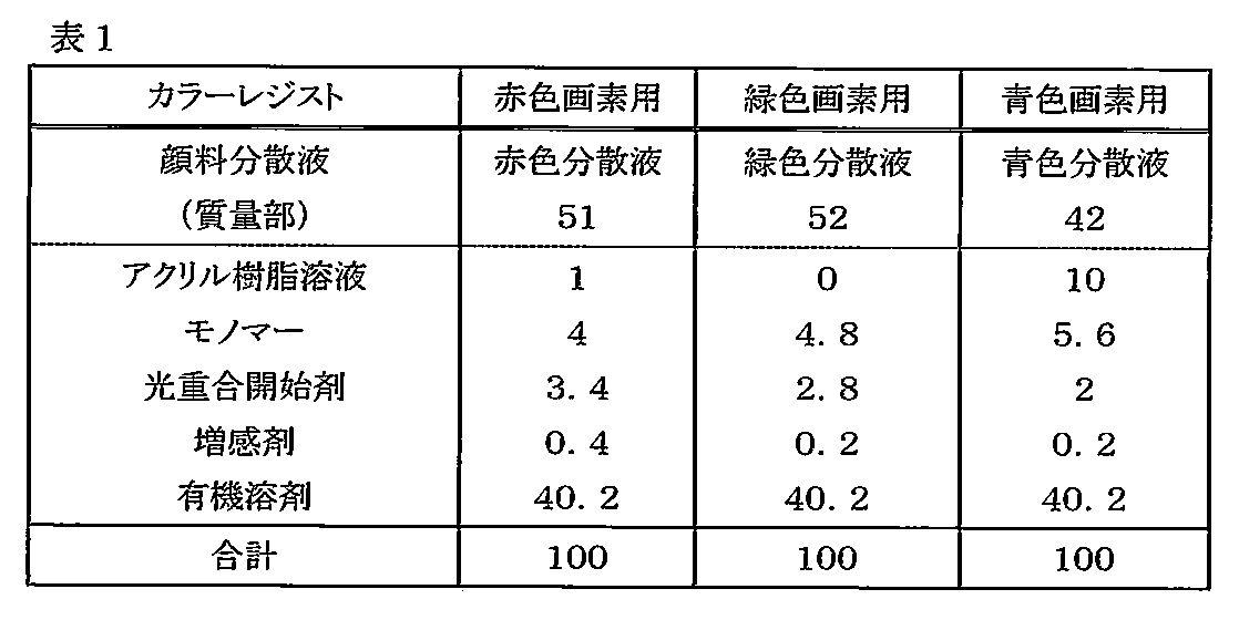
(着色層形成用分散液)
着色層に分散する有機顔料として、例えば以下の顔料が用いられる。
緑色顔料:C.I.Pigment Green 58、C.I.Pigment Yellow 150
青色顔料:C.I.Pigment Blue 15、C.I.Pigment Violet 23
上記の顔料を用いて、赤色、緑色、及び青色の各色分散液が生成される。
赤色顔料:C.I.Pigment Red 254 18質量部
赤色顔料:C.I.Pigment Red 177 2質量部
アクリルワニス(固形分20質量%) 108質量部
上記の組成の混合物を均一に攪拌した後、ガラスビーズを用いて、サンドミルで5時間分散し、5μmフィルタで濾過を行ない、赤色分散液が生成される。
緑色顔料:C.I.Pigment Green 58 16質量部
緑色顔料:C.I.Pigment Yellow 150 8質量部
アクリルワニス(固形分20質量%) 102質量部
上記の組成の混合物に対して、赤色分散液と同様の生成方法を用いて、緑色分散液が生成される。
青色顔料:C.I.Pigment Blue 15 50質量部
青色顔料:C.I.Pigment Violet 23 2質量部
分散剤 6質量部
アクリルワニス(固形分20質量%) 200質量部
上記の組成の混合物に対して、赤色分散液と同様の生成方法を用いて、青色分散液が生成される。
露光・現像及び硬膜後、それぞれ着色画素の膜厚は2μmであるとする。線状パターン7の部分にある遮光パターン6上の着色層の膜厚が厚くならないように、着色層の形成においては、例えば透過率の低いグレートーンであるフォトマスクが露光に用いられる。
本実施形態においては、上記の各実施形態で説明された液晶表示装置1又は液晶表示装置18の視野角制御の作用について説明する。なお、本実施形態では、上記図1に示す液晶表示用基板2を備える液晶表示装置1について説明するが、液晶表示用基板2Aを備える液晶表示装置1又は液晶表示装置18についても同様である。
本実施形態においては、上記各実施形態で説明された液晶表示装置1又は液晶表示装置18の変形例について説明する。なお、本実施形態では、上記図1に示す液晶表示用基板2を備える液晶表示装置1の変形例について説明するが、液晶表示用基板2Aを備える液晶表示装置1又は液晶表示装置18についても同様に変形可能である。
本実施形態においては、上記各実施形態において、低電圧で液晶4を駆動するための構成について説明する。
Claims (14)
- 平面形状において向かい合う平行な辺を持つ多角形画素又は多角形サブピクセルと、
前記多角形画素又は前記多角形サブピクセルの前記向かい合う平行な辺に備えられ、斜め光を透過する線状パターンと
を具備する液晶表示用基板。 - 前記線状パターンは、平面形状において、線状の透明パターンを線状の遮光パターンで挟む構成を持つ、請求項1の液晶表示用基板。
- 前記線状パターンは、平面形状において、前記透明パターンの中央、かつ、線状の長手方向に遮光部をさらに具備する、請求項2の液晶表示用基板。
- 前記線状パターン上に形成される透明導電膜をさらに具備する、請求項1の液晶表示用基板。
- 一方の表面上に前記線状パターンが形成されている透明基板と、
前記線状パターンが形成されている前記透明基板の前記表面に積層される透明導電膜と、
前記透明導電膜上に形成される前記多角形画素又は前記多角形サブピクセルのカラーフィルタと
を具備する請求項1の液晶表示用基板。 - 前記カラーフィルタとして、少なくとも赤カラーフィルタ、緑カラーフィルタ、青カラーフィルタのうちの2以上が用いられる、請求項5の液晶表示用基板。
- 前記多角形画素又は前記多角形サブピクセルの前記平面形状は、長方形、平行四辺形、くの字状に折れ曲がった多角形のうちのいずれかである、請求項1の液晶表示用基板。
- 前記透明パターンの形成部分は、前記他の部分よりも厚いことを特徴とする請求項1の液晶表示用基板。
- 平面形状において向かい合う平行な辺を持つ多角形画素又は多角形サブピクセルと、前記多角形画素又は前記多角形サブピクセルの前記向かい合う平行な辺に備えられた斜め光を透過する線状パターンとを具備する液晶表示用基板と、
前記液晶表示用基板と液晶層を介して対向し、前記液晶層の液晶を駆動するアクティブ素子を備えるアレイ基板と
を具備する液晶表示装置。 - 前記アレイ基板は、前記多角形画素又は前記多角形サブピクセルごとに、前記液晶を駆動するために異なる電位が印加される第1電極と第2電極とを具備する請求項9の液晶表示装置。
- 前記第1電極は、前記液晶を駆動するアクティブ素子と接続された第1の櫛歯状パターンであり、
前記第2電極は、絶縁層を介して前記第1電極の下に配設された第2の櫛歯状パターンであり、水平方向において、前記多角形画素又は前記多角形サブマトリクスを垂直方向に2分する中心軸の反対方向に、前記第1電極の端部からはみ出た位置に配置される
請求項10の液晶表示装置。 - 前記多角形画素又は前記多角形サブマトリクスごとに、2以上の前記アクティブ素子を備えており、
前記多角形画素又は前記多角形サブマトリクスごとに備えられている前記2以上のアクティブ素子は、前記多角形画素又は前記多角形サブマトリクスごとに、前記第1電極における電気的に独立の2以上の部分に、それぞれ接続される
請求項10の液晶表示装置。 - 前記第1電極及び前記第2電極は、可視域で透明な導電性金属酸化物によって形成される、請求項10の液晶表示装置。
- 前記液晶は負の誘電率異方性を有する、請求項9の液晶表示装置。
Priority Applications (4)
| Application Number | Priority Date | Filing Date | Title |
|---|---|---|---|
| CN2011800666290A CN103339557A (zh) | 2011-02-01 | 2011-05-24 | 液晶显示用基板及液晶显示装置 |
| EP11857471.4A EP2672315A4 (en) | 2011-02-01 | 2011-05-24 | Liquid crystal display substrate and liquid crystal display device |
| KR1020137020363A KR20140008338A (ko) | 2011-02-01 | 2011-05-24 | 액정 표시용 기판 및 액정 표시 장치 |
| US13/946,737 US20130300989A1 (en) | 2011-02-01 | 2013-07-19 | Substrate for liquid crystal display and liquid crystal display device |
Applications Claiming Priority (2)
| Application Number | Priority Date | Filing Date | Title |
|---|---|---|---|
| JP2011019833A JP5152352B2 (ja) | 2011-02-01 | 2011-02-01 | 液晶表示用基板及び液晶表示装置 |
| JP2011-019833 | 2011-02-01 |
Related Child Applications (1)
| Application Number | Title | Priority Date | Filing Date |
|---|---|---|---|
| US13/946,737 Continuation US20130300989A1 (en) | 2011-02-01 | 2013-07-19 | Substrate for liquid crystal display and liquid crystal display device |
Publications (1)
| Publication Number | Publication Date |
|---|---|
| WO2012105067A1 true WO2012105067A1 (ja) | 2012-08-09 |
Family
ID=46602304
Family Applications (1)
| Application Number | Title | Priority Date | Filing Date |
|---|---|---|---|
| PCT/JP2011/061876 Ceased WO2012105067A1 (ja) | 2011-02-01 | 2011-05-24 | 液晶表示用基板及び液晶表示装置 |
Country Status (7)
| Country | Link |
|---|---|
| US (1) | US20130300989A1 (ja) |
| EP (1) | EP2672315A4 (ja) |
| JP (1) | JP5152352B2 (ja) |
| KR (1) | KR20140008338A (ja) |
| CN (1) | CN103339557A (ja) |
| TW (1) | TWI467279B (ja) |
| WO (1) | WO2012105067A1 (ja) |
Cited By (3)
| Publication number | Priority date | Publication date | Assignee | Title |
|---|---|---|---|---|
| US20140063386A1 (en) * | 2012-09-04 | 2014-03-06 | Au Optronics Corp. | Peep-proof display apparatus and driving method thereof |
| US20140340621A1 (en) * | 2013-05-20 | 2014-11-20 | Infovision Optoelectronics (Kunshan) Co., Ltd. | Liquid crystal display device |
| TWI476495B (zh) * | 2012-09-26 | 2015-03-11 | Au Optronics Corp | 具有位置資訊之顯示器 |
Families Citing this family (14)
| Publication number | Priority date | Publication date | Assignee | Title |
|---|---|---|---|---|
| WO2014103777A1 (ja) * | 2012-12-27 | 2014-07-03 | 凸版印刷株式会社 | 液晶表示装置、液晶表示装置用基板、及び液晶表示装置用基板の製造方法 |
| CN105308499B (zh) * | 2013-06-28 | 2017-08-29 | 夏普株式会社 | 液晶显示装置 |
| KR102150080B1 (ko) * | 2013-09-12 | 2020-09-01 | 삼성디스플레이 주식회사 | 표시 패널 및 이를 포함하는 표시 장치 |
| JP2015090435A (ja) * | 2013-11-06 | 2015-05-11 | 株式会社ジャパンディスプレイ | 液晶表示装置 |
| CN104932167B (zh) * | 2015-06-25 | 2018-06-19 | 深圳市华星光电技术有限公司 | 蓝相液晶显示装置及其驱动方法 |
| JP6848043B2 (ja) | 2016-08-08 | 2021-03-24 | 昆山龍騰光電有限公司 | 視野角切替可能な液晶表示装置及びその視野角切替方法 |
| KR102716926B1 (ko) | 2016-12-26 | 2024-10-11 | 엘지디스플레이 주식회사 | 터치 스크린 일체형 표시장치 |
| CN106814506B (zh) * | 2017-04-01 | 2018-09-04 | 深圳市华星光电技术有限公司 | 一种液晶显示面板及装置 |
| CN107843993B (zh) * | 2017-11-09 | 2020-01-10 | 维沃移动通信有限公司 | 一种显示屏可视角度的控制方法、移动终端及计算机存储介质 |
| JP2019090954A (ja) * | 2017-11-16 | 2019-06-13 | シャープ株式会社 | カラーフィルタ基板及びその製造方法、並びに表示パネル |
| CN108549166B (zh) * | 2018-04-17 | 2021-11-02 | 京东方科技集团股份有限公司 | 防窥子像素单元及其制作方法以及显示装置及其驱动方法 |
| CN110376773B (zh) * | 2019-07-22 | 2022-02-11 | 昆山龙腾光电股份有限公司 | 视角可切换液晶显示装置的驱动方法 |
| CN110456580B (zh) * | 2019-08-26 | 2022-04-29 | 京东方科技集团股份有限公司 | 一种显示基板及其控制方法、显示面板、显示装置 |
| CN114326199B (zh) * | 2021-12-31 | 2024-04-02 | 厦门天马微电子有限公司 | 显示面板和显示装置 |
Citations (8)
| Publication number | Priority date | Publication date | Assignee | Title |
|---|---|---|---|---|
| JP2001324710A (ja) * | 2000-05-17 | 2001-11-22 | Nec Corp | 液晶表示装置およびその製造方法ならびに駆動方法 |
| JP3322197B2 (ja) | 1997-12-17 | 2002-09-09 | 松下電器産業株式会社 | 液晶表示装置 |
| JP2005274777A (ja) * | 2004-03-23 | 2005-10-06 | Sharp Corp | 液晶表示装置および電子機器 |
| JP2007065046A (ja) | 2005-08-29 | 2007-03-15 | Casio Comput Co Ltd | 液晶表示素子及び液晶表示装置 |
| JP2009105424A (ja) | 2008-12-12 | 2009-05-14 | Kobe Steel Ltd | 薄膜トランジスタ基板および表示デバイス |
| JP4367206B2 (ja) | 2004-04-01 | 2009-11-18 | セイコーエプソン株式会社 | 視角制御素子、液晶表示装置、電子機器 |
| JP2010128126A (ja) | 2008-11-27 | 2010-06-10 | Epson Imaging Devices Corp | 液晶表示装置 |
| JP2010224382A (ja) * | 2009-03-25 | 2010-10-07 | Sony Corp | 電気光学装置および電子機器 |
Family Cites Families (7)
| Publication number | Priority date | Publication date | Assignee | Title |
|---|---|---|---|---|
| JP2006309105A (ja) * | 2005-03-30 | 2006-11-09 | Casio Comput Co Ltd | 液晶表示素子 |
| KR20060106168A (ko) * | 2005-04-06 | 2006-10-12 | 삼성전자주식회사 | 액정표시장치 |
| KR101180718B1 (ko) * | 2005-12-29 | 2012-09-07 | 엘지디스플레이 주식회사 | 횡전계형 액정표시장치용 어레이 기판 및 그 제조 방법 |
| JP5061505B2 (ja) * | 2006-05-25 | 2012-10-31 | 日本電気株式会社 | 横電界方式のアクティブマトリクス型液晶表示装置 |
| KR101268954B1 (ko) * | 2006-06-29 | 2013-05-30 | 엘지디스플레이 주식회사 | 시야각 제어가 가능한 액정 표시 장치 및 그의 제조 방법 |
| KR20080111939A (ko) * | 2007-06-20 | 2008-12-24 | 엘지디스플레이 주식회사 | 액정 표시 장치 |
| KR100914785B1 (ko) * | 2007-12-26 | 2009-08-31 | 엘지디스플레이 주식회사 | 액정표시장치 |
-
2011
- 2011-02-01 JP JP2011019833A patent/JP5152352B2/ja not_active Expired - Fee Related
- 2011-05-24 KR KR1020137020363A patent/KR20140008338A/ko not_active Withdrawn
- 2011-05-24 WO PCT/JP2011/061876 patent/WO2012105067A1/ja not_active Ceased
- 2011-05-24 EP EP11857471.4A patent/EP2672315A4/en not_active Withdrawn
- 2011-05-24 CN CN2011800666290A patent/CN103339557A/zh active Pending
- 2011-07-14 TW TW100124860A patent/TWI467279B/zh not_active IP Right Cessation
-
2013
- 2013-07-19 US US13/946,737 patent/US20130300989A1/en not_active Abandoned
Patent Citations (8)
| Publication number | Priority date | Publication date | Assignee | Title |
|---|---|---|---|---|
| JP3322197B2 (ja) | 1997-12-17 | 2002-09-09 | 松下電器産業株式会社 | 液晶表示装置 |
| JP2001324710A (ja) * | 2000-05-17 | 2001-11-22 | Nec Corp | 液晶表示装置およびその製造方法ならびに駆動方法 |
| JP2005274777A (ja) * | 2004-03-23 | 2005-10-06 | Sharp Corp | 液晶表示装置および電子機器 |
| JP4367206B2 (ja) | 2004-04-01 | 2009-11-18 | セイコーエプソン株式会社 | 視角制御素子、液晶表示装置、電子機器 |
| JP2007065046A (ja) | 2005-08-29 | 2007-03-15 | Casio Comput Co Ltd | 液晶表示素子及び液晶表示装置 |
| JP2010128126A (ja) | 2008-11-27 | 2010-06-10 | Epson Imaging Devices Corp | 液晶表示装置 |
| JP2009105424A (ja) | 2008-12-12 | 2009-05-14 | Kobe Steel Ltd | 薄膜トランジスタ基板および表示デバイス |
| JP2010224382A (ja) * | 2009-03-25 | 2010-10-07 | Sony Corp | 電気光学装置および電子機器 |
Non-Patent Citations (1)
| Title |
|---|
| See also references of EP2672315A4 * |
Cited By (5)
| Publication number | Priority date | Publication date | Assignee | Title |
|---|---|---|---|---|
| US20140063386A1 (en) * | 2012-09-04 | 2014-03-06 | Au Optronics Corp. | Peep-proof display apparatus and driving method thereof |
| US8988643B2 (en) * | 2012-09-04 | 2015-03-24 | Au Optronics Corp. | Peep-proof display apparatus and driving method thereof |
| TWI476495B (zh) * | 2012-09-26 | 2015-03-11 | Au Optronics Corp | 具有位置資訊之顯示器 |
| US20140340621A1 (en) * | 2013-05-20 | 2014-11-20 | Infovision Optoelectronics (Kunshan) Co., Ltd. | Liquid crystal display device |
| US9684199B2 (en) * | 2013-05-20 | 2017-06-20 | Infovision Optoelectronics (Kunshan) Co., Ltd. | Liquid crystal display substrate and device |
Also Published As
| Publication number | Publication date |
|---|---|
| EP2672315A1 (en) | 2013-12-11 |
| US20130300989A1 (en) | 2013-11-14 |
| CN103339557A (zh) | 2013-10-02 |
| JP2012159729A (ja) | 2012-08-23 |
| EP2672315A4 (en) | 2014-07-30 |
| TWI467279B (zh) | 2015-01-01 |
| JP5152352B2 (ja) | 2013-02-27 |
| TW201234082A (en) | 2012-08-16 |
| KR20140008338A (ko) | 2014-01-21 |
Similar Documents
| Publication | Publication Date | Title |
|---|---|---|
| JP5152352B2 (ja) | 液晶表示用基板及び液晶表示装置 | |
| JP5578132B2 (ja) | 液晶表示装置 | |
| TWI464492B (zh) | 傾斜電場液晶顯示裝置用彩色濾光片基板及液晶顯示裝置 | |
| TWI497164B (zh) | 液晶顯示裝置 | |
| TWI464489B (zh) | 彩色濾光片基板及液晶顯示裝置 | |
| TWI470317B (zh) | 半透過型液晶顯示裝置用基板、彩色濾光片基板及液晶顯示裝置 | |
| JP5083467B2 (ja) | 液晶表示装置用カラーフィルタ基板および液晶表示装置 | |
| JP5609791B2 (ja) | 液晶表示用の対向基板及び液晶表示装置 | |
| KR101822691B1 (ko) | 액정 표시 기판 및 액정 표시 장치 | |
| JP5158133B2 (ja) | 垂直配向液晶表示装置用基板および垂直配向液晶表示装置 |
Legal Events
| Date | Code | Title | Description |
|---|---|---|---|
| 121 | Ep: the epo has been informed by wipo that ep was designated in this application |
Ref document number: 11857471 Country of ref document: EP Kind code of ref document: A1 |
|
| REEP | Request for entry into the european phase |
Ref document number: 2011857471 Country of ref document: EP |
|
| WWE | Wipo information: entry into national phase |
Ref document number: 2011857471 Country of ref document: EP |
|
| ENP | Entry into the national phase |
Ref document number: 20137020363 Country of ref document: KR Kind code of ref document: A |
|
| NENP | Non-entry into the national phase |
Ref country code: DE |