WO2012105148A1 - Élément de conversion photoélectrique - Google Patents
Élément de conversion photoélectrique Download PDFInfo
- Publication number
- WO2012105148A1 WO2012105148A1 PCT/JP2011/080241 JP2011080241W WO2012105148A1 WO 2012105148 A1 WO2012105148 A1 WO 2012105148A1 JP 2011080241 W JP2011080241 W JP 2011080241W WO 2012105148 A1 WO2012105148 A1 WO 2012105148A1
- Authority
- WO
- WIPO (PCT)
- Prior art keywords
- transparent conductive
- conductive film
- film
- photoelectric conversion
- conversion element
- Prior art date
- Legal status (The legal status is an assumption and is not a legal conclusion. Google has not performed a legal analysis and makes no representation as to the accuracy of the status listed.)
- Ceased
Links
Images




Classifications
-
- H—ELECTRICITY
- H10—SEMICONDUCTOR DEVICES; ELECTRIC SOLID-STATE DEVICES NOT OTHERWISE PROVIDED FOR
- H10F—INORGANIC SEMICONDUCTOR DEVICES SENSITIVE TO INFRARED RADIATION, LIGHT, ELECTROMAGNETIC RADIATION OF SHORTER WAVELENGTH OR CORPUSCULAR RADIATION
- H10F77/00—Constructional details of devices covered by this subclass
- H10F77/10—Semiconductor bodies
- H10F77/16—Material structures, e.g. crystalline structures, film structures or crystal plane orientations
- H10F77/162—Non-monocrystalline materials, e.g. semiconductor particles embedded in insulating materials
- H10F77/166—Amorphous semiconductors
-
- H—ELECTRICITY
- H10—SEMICONDUCTOR DEVICES; ELECTRIC SOLID-STATE DEVICES NOT OTHERWISE PROVIDED FOR
- H10F—INORGANIC SEMICONDUCTOR DEVICES SENSITIVE TO INFRARED RADIATION, LIGHT, ELECTROMAGNETIC RADIATION OF SHORTER WAVELENGTH OR CORPUSCULAR RADIATION
- H10F10/00—Individual photovoltaic cells, e.g. solar cells
- H10F10/10—Individual photovoltaic cells, e.g. solar cells having potential barriers
- H10F10/16—Photovoltaic cells having only PN heterojunction potential barriers
- H10F10/164—Photovoltaic cells having only PN heterojunction potential barriers comprising heterojunctions with Group IV materials, e.g. ITO/Si or GaAs/SiGe photovoltaic cells
- H10F10/165—Photovoltaic cells having only PN heterojunction potential barriers comprising heterojunctions with Group IV materials, e.g. ITO/Si or GaAs/SiGe photovoltaic cells the heterojunctions being Group IV-IV heterojunctions, e.g. Si/Ge, SiGe/Si or Si/SiC photovoltaic cells
- H10F10/166—Photovoltaic cells having only PN heterojunction potential barriers comprising heterojunctions with Group IV materials, e.g. ITO/Si or GaAs/SiGe photovoltaic cells the heterojunctions being Group IV-IV heterojunctions, e.g. Si/Ge, SiGe/Si or Si/SiC photovoltaic cells the Group IV-IV heterojunctions being heterojunctions of crystalline and amorphous materials, e.g. silicon heterojunction [SHJ] photovoltaic cells
-
- H—ELECTRICITY
- H10—SEMICONDUCTOR DEVICES; ELECTRIC SOLID-STATE DEVICES NOT OTHERWISE PROVIDED FOR
- H10F—INORGANIC SEMICONDUCTOR DEVICES SENSITIVE TO INFRARED RADIATION, LIGHT, ELECTROMAGNETIC RADIATION OF SHORTER WAVELENGTH OR CORPUSCULAR RADIATION
- H10F71/00—Manufacture or treatment of devices covered by this subclass
- H10F71/138—Manufacture of transparent electrodes, e.g. transparent conductive oxides [TCO] or indium tin oxide [ITO] electrodes
-
- H—ELECTRICITY
- H10—SEMICONDUCTOR DEVICES; ELECTRIC SOLID-STATE DEVICES NOT OTHERWISE PROVIDED FOR
- H10F—INORGANIC SEMICONDUCTOR DEVICES SENSITIVE TO INFRARED RADIATION, LIGHT, ELECTROMAGNETIC RADIATION OF SHORTER WAVELENGTH OR CORPUSCULAR RADIATION
- H10F77/00—Constructional details of devices covered by this subclass
- H10F77/20—Electrodes
- H10F77/244—Electrodes made of transparent conductive layers, e.g. transparent conductive oxide [TCO] layers
-
- Y—GENERAL TAGGING OF NEW TECHNOLOGICAL DEVELOPMENTS; GENERAL TAGGING OF CROSS-SECTIONAL TECHNOLOGIES SPANNING OVER SEVERAL SECTIONS OF THE IPC; TECHNICAL SUBJECTS COVERED BY FORMER USPC CROSS-REFERENCE ART COLLECTIONS [XRACs] AND DIGESTS
- Y02—TECHNOLOGIES OR APPLICATIONS FOR MITIGATION OR ADAPTATION AGAINST CLIMATE CHANGE
- Y02E—REDUCTION OF GREENHOUSE GAS [GHG] EMISSIONS, RELATED TO ENERGY GENERATION, TRANSMISSION OR DISTRIBUTION
- Y02E10/00—Energy generation through renewable energy sources
- Y02E10/50—Photovoltaic [PV] energy
- Y02E10/52—PV systems with concentrators
Definitions
- the present invention relates to a photoelectric conversion element.
- Patent Document 1 includes a first conductive type crystalline semiconductor substrate having a front surface and a back surface, and light is incident from the front surface side, an amorphous semiconductor film formed on the surface of the crystalline semiconductor substrate, A first transparent conductive film formed on the amorphous semiconductor film and containing a metal dopant of 1.5 mass% or more and 5 mass% or less, and a first transparent conductive film formed on the back surface of the crystalline semiconductor substrate A photovoltaic device comprising a second transparent conductive film containing a metal dopant less than the content of the metal dopant is disclosed.
- the photoelectric conversion element according to the present invention includes a first main surface and a crystalline semiconductor substrate including a second main surface facing the first main surface, and a first semiconductor formed on the first main surface of the crystalline semiconductor substrate.
- a second transparent conductive film having a film thickness equal to or greater than that of the transparent conductive film, and a metal layer formed on the second transparent conductive film were provided.
- the characteristics of the photoelectric conversion element can be improved.
- FIG. 3 is a cross-sectional view taken along line AA in FIG. 2 and a cross-sectional view of the photoelectric conversion element.
- the film thickness of a transparent conductive film is changed, it is a figure which shows a mode that the reflectance characteristic with respect to the wavelength of incident light changes.
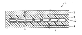
- FIG. 1 is a cross-sectional view of the solar cell module 1.
- the solar cell module 1 includes a plurality of photoelectric conversion elements 10, a plurality of wiring members 5, a sealing material 3, a first protection member 2, and a second protection member 4.
- light such as sunlight is mainly incident from the light receiving surface side of the first protective member 2 (the side opposite to the side where the photoelectric conversion element 10 is disposed with respect to the first protective member 2). explain.
- the plurality of photoelectric conversion elements 10 are arranged in alignment. Each wiring member 5 electrically connects adjacent photoelectric conversion elements 10 to each other. Thereby, the some photoelectric conversion element 10 is connected in series or in parallel.
- the first protective member 2 is disposed on the light receiving surface side of the photoelectric conversion element 10.
- the 1st protection member 2 can be comprised using glass, translucent resin, etc., for example.
- the second protective member 4 is disposed on the back side of the photoelectric conversion element 10.
- the 2nd protection member 4 can be comprised using the resin film which interposed metal foil, such as aluminum foil.
- the sealing material 3 is filled between the photoelectric conversion element 10 and the first protective member 2 and between the photoelectric conversion element 10 and the second protective member 4.
- the plurality of photoelectric conversion elements 10 are sealed with the sealing material 3.
- the sealing material 3 can be comprised using resin which has translucency, such as an ethylene-vinyl acetate copolymer (EVA) and polyvinyl butyral (PVB), for example.
- EVA ethylene-vinyl acetate copolymer
- PVB polyvinyl butyral
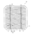
- FIG. 2 is a plan view of the light receiving surface side of the photoelectric conversion element 10.
- FIG. 3 is a plan view of the back surface side of the photoelectric conversion element 10.
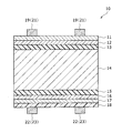
- 4 is a cross-sectional view taken along the line AA in FIG. 2, and is a cross-sectional view of the photoelectric conversion element 10.
- the “light receiving surface” means a surface on which light such as sunlight is mainly incident.
- the “back surface” means a surface opposite to the light receiving surface.
- the photoelectric conversion element 10 includes, from the light incident side, a transparent conductive film 11, a p-type amorphous silicon film 12, an i-type amorphous silicon film 13, an n-type single crystal silicon substrate 14, and an i-type amorphous material.
- a porous silicon film 15, an n-type amorphous silicon film 16, a transparent conductive film 17, and a metal film 18 are laminated.
- a collector electrode 21 including a plurality of finger electrode portions 20 and a plurality of bus bar electrode portions 19 is provided on the light receiving surface side of the photoelectric conversion element 10.
- a collector electrode 23 including a plurality of protruding electrode portions 22 is provided on the back surface side of the photoelectric conversion element 10.
- the i-type amorphous silicon film 13 is laminated on the light-receiving surface of the n-type single crystal silicon substrate 14.
- the film thickness of the i-type amorphous silicon film 13 is preferably 10 nm or more and 20 nm or less, for example.
- the i-type amorphous silicon film 13 can be formed using, for example, a plasma CVD method.
- the p-type amorphous silicon film 12 is laminated on the i-type amorphous silicon film 13.
- the thickness of the p-type amorphous silicon film 12 is preferably 6 nm or more and 80 nm or less.
- the p-type amorphous silicon film 12 can be formed using, for example, a plasma CVD method.
- the transparent conductive film 11 is laminated on the p-type amorphous silicon film 12.
- the transparent conductive film 11 is made of, for example, a metal oxide such as indium oxide (In 2 O 3 ), zinc oxide (ZnO), tin oxide (SnO 2 ), and titanium oxide (TiO 2 ) having a polycrystalline structure. It is configured to include at least one. These metal oxides contain dopants such as tin (Sn), zinc (Zn), tungsten (W), antimony (Sb), titanium (Ti), aluminum (Al), cerium (Ce), and gallium (Ga). It may be doped. The concentration of the dopant can be 0 to 20 wt%.
- the transparent conductive film 11 is described as being formed using indium tin oxide (ITO).
- the film thickness of the transparent conductive film 11 is preferably 100 nm, for example.
- the bus bar electrode portion 19 is an electrode member provided for collecting and taking out the electricity generated in the photoelectric conversion element 10.
- the bus bar electrode portion 19 is preferably arranged so as to collect electricity collected in the finger electrode portion 20 described later as evenly as possible.
- a plurality of bus bar electrode portions 19 may be provided.
- the bus bar electrode portions 19 are preferably formed in parallel to each other on the transparent conductive film 11.
- the width of the bus bar electrode portion 19 is appropriately determined according to the magnitude of the current to be collected, the thickness of the bus bar electrode portion 19, and the like, for example, 1.5 mm.
- Finger electrode part 20 is an electrode member provided for collecting and taking out the electricity generated in photoelectric conversion element 10 together with bus bar electrode part 19.
- the finger electrode unit 20 is preferably arranged so that current collection is performed uniformly from within the surface of the photoelectric conversion element 10.
- the finger electrode portion 20 is disposed so as to cross the bus bar electrode portion 19 and be electrically connected thereto.
- the plurality of finger electrode portions 20 are arranged in parallel to each other.
- the width of the finger electrode portion 20 is appropriately determined according to the magnitude of the current to be collected, the thickness of the finger electrode portion 20, and the like, for example, 100 ⁇ m.
- the pitch of the finger electrode portions 20 is preferably 2 mm, for example.
- the bus bar electrode portion 19 and the finger electrode portion 20 are conductive materials, such as Ag (silver), Cu (copper), Al (aluminum), Ti (titanium), Ni (nickel), and Cr (chromium). It can be comprised with the metal and the alloy containing 1 or more types of these metals. Moreover, the bus-bar electrode part 19 and the finger electrode 20 may be comprised by the laminated body of the some conductive layer which consists of the said metal and alloy, for example.
- the bus bar electrode portion 19 and the finger electrode portion 20 can be formed using a conductive paste such as an Ag paste, for example.
- the bus bar electrode portion 19 and the finger electrode portion 20 will be described as being formed using Ag.
- the i-type amorphous silicon film 15 is laminated on the back surface of the n-type single crystal silicon substrate 14.
- the film thickness of the i-type amorphous silicon film 15 is preferably, for example, not less than 3.5 nm and not more than 8 nm.
- the i-type amorphous silicon film 15 can be formed using, for example, a plasma CVD (chemical vapor deposition) method.
- the n-type amorphous silicon film 16 is stacked on the i-type amorphous silicon film 15.
- the film thickness of the n-type amorphous silicon film 16 is preferably 2 nm or more and 8 nm or less, for example.
- the n-type amorphous silicon film 16 can be formed using, for example, a plasma CVD method.
- the transparent conductive film 17 is laminated on the n-type amorphous silicon film 16.
- the transparent conductive film 17 is made of, for example, a metal oxide such as indium oxide (In 2 O 3 ), zinc oxide (ZnO), tin oxide (SnO 2 ), and titanium oxide (TiO 2 ) having a polycrystalline structure. It is configured to include at least one.
- These metal oxides contain dopants such as tin (Sn), zinc (Zn), tungsten (W), antimony (Sb), titanium (Ti), aluminum (Al), cerium (Ce), and gallium (Ga). It may be doped. The concentration of the dopant can be 0 to 20 wt%.
- the transparent conductive film 17 is described as being formed using indium tin oxide (ITO).
- ITO indium tin oxide
- the film thickness of the transparent conductive film 17 is preferably equal to or greater than the thickness of the transparent conductive film 11, and is preferably greater than or equal to 100 nm and smaller than 150 nm, for example.
- the metal film 18 is laminated on the transparent conductive film 17.
- the metal film 18 is laminated so as to cover almost the entire surface of the formation region of the transparent conductive film 17.
- “so as to cover substantially the entire surface of the formation region of the transparent conductive film 17” means a state that can be regarded as covering substantially the entire surface of the transparent conductive film 17. This includes a state in which a part of the metal film 18 laminated is missing.
- the area of the formation region of the metal film 18 is preferably in the range of 90% to 100% of the area of the formation region of the transparent conductive film 17.
- the metal film 18 has a higher light reflectivity for light in the infrared region of the wavelength range of about 800 nm to 1200 nm and higher conductivity than the transparent conductive film 17 in the wavelength region used in the photoelectric conversion element 10. It is preferable to use a metal. For this reason, the metal film 18 can be formed of a metal such as Ag, Al, Cu, Ni and Cr, or an alloy containing one or more of these metals.
- the metal film 18 may be composed of a laminate of a plurality of films made of the above metals or alloys.
- the metal film 18 is more preferably made of Ag having a high reflectance at wavelengths in the infrared region.
- the film thickness of the metal film 18 is preferably, for example, 150 nm or more and 1000 nm or less, and more preferably 300 nm or more and 500 nm.
- the metal film 18 is described as being formed using Ag.
- the protruding electrode part 22 is an electrode member provided for collecting and taking out the electricity generated in the photoelectric conversion element 10.
- the protruding electrode portion 22 is preferably disposed so as to collect electricity collected in the metal film 18 as evenly as possible.
- a plurality of protruding electrode portions 22 may be provided.
- the protruding electrode portions 22 are preferably formed in parallel to each other on the transparent conductive film 11.
- the width of the protruding electrode portion 22 is appropriately determined according to the magnitude of the current to be collected, the thickness of the bus bar electrode portion 19 and the like, and is preferably about 0.05 ⁇ m to 2 mm, for example. It is more preferably about 0.05 ⁇ m to 0.5 mm.
- the film thickness of the protruding electrode portion 22 is preferably thicker than that of the metal film 18, and is preferably 5 ⁇ m to 20 ⁇ m, for example. Since the material and forming method of the protruding electrode portion 22 are the same as those of the bus bar electrode portion 19, detailed description is omitted.
- each film thickness illustrated above can be measured using a transmission electron microscope (TEM). And each film thickness illustrated above has shown the average film thickness of the thickness along the lamination direction in the cross section of the photoelectric conversion element 10.
- TEM transmission electron microscope
- each of the transparent conductive films 11 and 17 will be described in detail in consideration of the roles of the transparent conductive film 11 and the transparent conductive film 17.
- the transparent conductive film 11 will be described in detail.
- One of the roles of the transparent conductive film 11 disposed on the light receiving surface side is to suppress surface reflection of the incident light on the transparent conductive film 11.
- the refractive index of the transparent conductive film 11 is preferably between the refractive index of the medium on the incident side of the transparent conductive film 11 and the refractive index of the medium on the transmission side of the transparent conductive film 11.
- the medium on the incident side of the transparent conductive film 11 is the sealing material 3, and as shown in FIG. Since it is the crystalline silicon film 12, the refractive index of the transparent conductive film 11 is preferably between the refractive index of the sealing material 3 and the refractive index of the p-type amorphous silicon film 12.
- the transparent conductive film 11 preferably reduces the reflectance of light in the wavelength region of 400 nm to 600 nm where the intensity of the sunlight spectrum is strong.
- FIG. 5 is a diagram illustrating how the reflectance characteristics with respect to the wavelength of incident light that is incident from the vertical direction on the surface of the photoelectric conversion element 10 change when the film thickness of the transparent conductive film 11 is changed. As shown in FIG. 5, the reflectance is remarkably low in the wavelength region of 400 n to 600 nm when the transparent conductive film 11 is 100 nm. Therefore, the transparent conductive film 11 is preferably 100 nm.
- the transparent conductive film 17 is preferably between the refractive index of the medium on the incident side of the transparent conductive film 17 and the refractive index of the medium on the transmission side of the transparent conductive film 17.
- the medium on the incident side of the transparent conductive film 17 is the n-type amorphous silicon film 16
- the medium on the transmission side of the transparent conductive film 17 is the metal film 18.
- the refractive index of the transparent conductive film 17 is preferably between the refractive index of the n-type amorphous silicon film 16 and the refractive index of the metal film 18.
- FIG. 6 is a diagram showing how the reflectance characteristics with respect to the incident angle change when the film thickness of the transparent conductive film 17 is changed.
- the transparent conductive film 17 does not absorb light at wavelengths in the infrared region.
- the light at the wavelength in the infrared region referred to here is mainly when the n-type amorphous silicon film 16, the transparent conductive film 17 and the metal film 18 are reflected on the transparent conductive film 17 or the metal film 18 in the laminated structure.
- the evanescent light which is the light which exudes slightly to the transparent conductive film 17 or the metal film 18 side. In such a case, as shown in FIG.
- the transparent conductive film 17 has a higher reflectance as the film thickness of the transparent conductive film 17 is increased, except when the film thickness of the transparent conductive film 17 is 0 nm.
- the film thickness of the transparent conductive film 17 is larger than the film thickness (100 nm) of the transparent conductive film 11, the reflectance is remarkably higher than that in the case where the incident angle is in the range of 50 ° to 60 ° and the film thickness is 50 nm. It is high.
- the metal film 18 and the n-type amorphous silicon film 16 are in direct contact, and the n-type amorphous silicon film 16 has a defect level.
- the film thickness of the transparent conductive film 17 should be greater than or equal to the film thickness of the transparent conductive film 11 on the assumption that the film thickness of the transparent conductive film 17 is not 0 nm. Below, it demonstrates on the assumption that the film thickness of the transparent conductive film 17 is not set to 0 nm.
- One of the reasons for realizing this function is due to absorption of evanescent light in the metal film 18. That is, in the photoelectric conversion element 10, the metal film 18 is laminated so as to cover substantially the entire area of the transparent conductive film 17. As a result, the influence of absorption of evanescent light in the metal film 18 is increased. However, in the photoelectric conversion element 10, the film thickness of the transparent conductive film 17 is greater than the film thickness of the transparent conductive film 11. Thereby, absorption of evanescent light in the metal film 18 can be suppressed.
- FIG. 7 is a diagram showing how the reflectance characteristics with respect to the incident angle change when the film thickness of the transparent conductive film 17 is changed in consideration of the absorption of evanescent light in the transparent conductive film 17.
- the film thickness of the transparent conductive film 17 is 50 nm
- the reflectance is lower than the other film thicknesses in the range of the incident angle of 50 ° to 80 °. Yes.
- the transparent conductive film 17 be equal to or larger than the film thickness (100 nm) of the transparent conductive film 11 and be set to 100 nm to 150 nm. More preferred.
- the evanescent light here is a laminated structure of the n-type amorphous silicon film 16, the transparent conductive film 17, and the metal film 18, and is totally reflected by the transparent conductive film 17 or the metal film 18. The light that exudes slightly to the 18th side.
- This evanescent light is absorbed by the transparent conductive film 17 and the metal film 18.
- the incident angle with respect to the transparent conductive film 17 is less than about 30 °, it is not totally reflected at the transparent conductive film 17 but is substantially totally reflected at the metal film 18. Therefore, when considering the reflectance, as shown in FIG.
- the manufacturing method of the photoelectric conversion element 10 is not limited to the manufacturing method shown in each process. In each step, for example, a sputtering method, a plasma CVD method, a screen printing method, a plating method, or the like can be appropriately used.
- the n-type single crystal silicon substrate 14 is carried into a vacuum chamber, and the i-type amorphous silicon film 13 is formed on the light receiving surface of the n-type single crystal silicon substrate 14 by using a plasma CVD method. Subsequently, a p-type amorphous silicon film 12 is formed on the i-type amorphous silicon film 13 using a plasma CVD method.
- an i-type amorphous silicon film 15 is formed on the n-type single crystal silicon substrate 14 using a plasma CVD method.
- an n-type amorphous silicon film 16 is formed on the i-type amorphous silicon film 15 using a plasma CVD method.
- a transparent conductive film 11 and a transparent conductive film 17 made of ITO are formed on the p-type amorphous silicon film 12 and the n-type amorphous silicon film 16 by sputtering, respectively.
- the amount of water (hydrogen amount) contained in the transparent conductive film 17 is larger than the amount of water (hydrogen amount) contained in the transparent conductive film 11.
- the amount of water contained in the transparent conductive films 11 and 17 can be measured by Rutherford Backscattering Spectrometry (RBS).
- RBS Rutherford Backscattering Spectrometry
- the amount of hydrogen can be obtained from the energy and yield of scattered ions that are elastically scattered, and the measured amount of hydrogen. Based on this, the amount of water in the film can be determined.
- a metal film 18 is formed on the transparent conductive film 17 using a sputtering method or a vapor deposition method.
- the collector electrode 21 and the collector electrode 23 are formed on the transparent conductive film 11 and the metal film 18 by screen printing, respectively.
- the photoelectric conversion element 10 In the photoelectric conversion element 10, light is incident on the n-type single crystal silicon substrate 14 from the transparent conductive film 11 side. At this time, light that has not contributed to power generation travels to the metal layer 18 through the transparent conductive film 17.
- the metal film 18 is made of Ag having a high reflectance at wavelengths in the infrared region. The metal film 18 is in contact with substantially the entire surface of the transparent conductive film 17 formation region. Thereby, the reflectance of the light in a back surface can be raised rather than the structure which only provides a finger electrode part and a bus-bar electrode part in a back surface like the past.
- the metal film 18 when the n-type amorphous silicon film 16 and the metal film 18 are in contact with each other, the metal atoms constituting the metal film 18 diffuse into the n-type amorphous silicon film 16 to generate defect levels, and carriers are trapped. Problem may occur.
- the metal film 18 is disposed so as not to be in direct contact with the n-type amorphous silicon film 16 by the transparent conductive film 17. Thereby, generation
- the film thickness of the transparent conductive film 17 is larger than that of the transparent conductive film 11.
- Increasing the thickness of the transparent conductive film 17 has an effect of reducing light absorption by the metal film 18 in the laminated structure of the transparent conductive film 17 and the metal film 18.
- the light reflectance in the laminated structure of the n-type amorphous silicon film 16, the transparent conductive film 17, and the metal film 18 can be improved.
- the light transmitted through the n-type amorphous silicon film 16 from the n-type single crystal silicon substrate 14 is reflected by the laminated structure of the n-type amorphous silicon film 16, the transparent conductive film 17 and the metal film 18 to be again n-type. It goes to the single crystal silicon substrate 14.
- the photoelectric conversion efficiency in the photoelectric conversion element 10 can be improved.
- an increase in the thickness of the transparent conductive film leads to an increase in manufacturing cost.
- the photoelectric conversion in the photoelectric conversion element 10 is positively increased by increasing the film thickness of the transparent conductive film 17 positioned on the back surface side. Priority is given to improving efficiency.
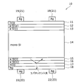
- FIG. 10 is a cross-sectional view of the photoelectric conversion element 10a. Since the difference between the photoelectric conversion element 10a and the photoelectric conversion element 10 is only the arrangement relationship between the metal film 18 and the protruding electrode portion 22 (collecting electrode 23), the difference will be mainly described.
- the protruding electrode part 22 is an electrode member provided for collecting and taking out the electricity generated in the photoelectric conversion element 10.
- the protruding electrode part 22 is preferably arranged so as to uniformly collect electricity generated in the photoelectric conversion element 10.
- a plurality of protruding electrode portions 22 may be provided.
- the protruding electrode portions 22 are formed in parallel to each other on the back surface side of the transparent conductive film 17. Of each surface of the protruding electrode portion 22, three surfaces other than the contact surface with the transparent conductive film 17 are in contact with the metal film 18.
- variety, film thickness, constituent material, and formation method of the protruding electrode part 22 are not specifically limited, Since it is the same as that of the protruding electrode part 22 of the photoelectric conversion element 10, detailed description is abbreviate
- the metal film 18 is laminated on the transparent conductive film 17 and the above three surfaces of the protruding electrode part 22.
- the metal film 18 is laminated so as to cover almost the entire surface of the formation region of the transparent conductive film 17.
- “so as to cover substantially the entire surface of the formation region of the transparent conductive film 17” means a state that can be regarded as covering substantially the entire surface of the transparent conductive film 17. This includes a state in which a part of the metal film 18 laminated is missing.
- the area of the formation region of the metal film 18 is smaller than the area of the formation region of the transparent conductive film 17.
- variety, film thickness, constituent material, and formation method of the metal film 18 are not specifically limited, Since it is the same as that of the metal film 18 of the photoelectric conversion element 10, detailed description is abbreviate
- the operation of the photoelectric conversion element 10a will be described.
- the photoelectric conversion element 10a light is incident on the n-type single crystal silicon substrate 14 from the transparent conductive film 11 side. At this time, light having a wavelength in the infrared region that has not contributed to power generation passes through the transparent conductive film 17. It goes to the metal layer 18 and the protruding electrode part 22.
- the metal film 18 and the protruding electrode portion 22 are configured using Ag having a high reflectance at wavelengths in the infrared region.
- the metal film 18 and the protruding electrode portion 22 are in contact with each other over substantially the entire surface of the transparent conductive film 17 formation region. Thereby, the reflectance of the light in a back surface can be raised rather than the structure which only provides a finger electrode part and a bus-bar electrode part in a back surface like the past.
- the film thickness of the transparent conductive film 17 is larger than that of the transparent conductive film 11.
- Increasing the thickness of the transparent conductive film 17 has an effect of reducing light absorption by the metal film 18 in the laminated structure of the transparent conductive film 17 and the metal film 18.
- the light reflectance in the laminated structure of the n-type amorphous silicon film 16, the transparent conductive film 17, and the metal film 18 can be improved.
- the light transmitted through the n-type amorphous silicon film 16 from the n-type single crystal silicon substrate 14 is reflected by the laminated structure of the n-type amorphous silicon film 16, the transparent conductive film 17 and the metal film 18 to be again n-type.
- the photoelectric conversion efficiency in the photoelectric conversion element 10 can be improved.
- an increase in the thickness of the transparent conductive film leads to an increase in manufacturing cost.
- the photoelectric conversion in the photoelectric conversion element 10a by positively increasing the film thickness of the transparent conductive film 17 positioned on the back surface side, the photoelectric conversion in the photoelectric conversion element 10a. Priority is given to improving efficiency.
- the metal film 18 and the protruding electrode part 22 have been described as being configured using Ag.
- the protruding electrode part 22 is made of a metal other than Ag.
- Al with low manufacturing cost can be used. Thereby, the manufacturing cost of the photoelectric conversion element 10 and the photoelectric conversion element 10a can be reduced.
- 1 solar cell module 2 first protective member, 3 encapsulant, 4 second protective member, 5 wiring member, 10 photoelectric conversion element, 11 transparent conductive film, 12 p-type amorphous silicon film, 13 i-type Amorphous silicon film, 14 n-type single crystal silicon substrate, 15 i-type amorphous silicon film, 16 n-type amorphous silicon film, 17 transparent conductive film, 18 metal film, 19 busbar electrode part, 20 finger electrode part , 21 collector electrode, 22 protruding electrode part, 23 collector electrode.
Landscapes
- Photovoltaic Devices (AREA)
Abstract
La présente invention se rapporte à un élément de conversion photoélectrique (10) qui contient un film conducteur transparent (11), un film de silicium amorphe de type p (12), un film de silicium amorphe de type i (13), un substrat de silicium monocristallin de type n (14), un film de silicium amorphe de type i (15), un film de silicium amorphe de type p (16), un film conducteur transparent (17) et un film métallique (18) ; l'épaisseur de film du film conducteur transparent (17) est supérieure ou égale à celle du film conducteur transparent (11).
Priority Applications (3)
| Application Number | Priority Date | Filing Date | Title |
|---|---|---|---|
| JP2012555707A JP5995204B2 (ja) | 2011-01-31 | 2011-12-27 | 光電変換素子 |
| EP11857839.2A EP2672522A4 (fr) | 2011-01-31 | 2011-12-27 | Élément de conversion photoélectrique |
| US13/954,252 US20130312829A1 (en) | 2011-01-31 | 2013-07-30 | Photoelectric conversion element |
Applications Claiming Priority (2)
| Application Number | Priority Date | Filing Date | Title |
|---|---|---|---|
| JP2011018382 | 2011-01-31 | ||
| JP2011-018382 | 2011-01-31 |
Related Child Applications (1)
| Application Number | Title | Priority Date | Filing Date |
|---|---|---|---|
| US13/954,252 Continuation US20130312829A1 (en) | 2011-01-31 | 2013-07-30 | Photoelectric conversion element |
Publications (1)
| Publication Number | Publication Date |
|---|---|
| WO2012105148A1 true WO2012105148A1 (fr) | 2012-08-09 |
Family
ID=46602378
Family Applications (1)
| Application Number | Title | Priority Date | Filing Date |
|---|---|---|---|
| PCT/JP2011/080241 Ceased WO2012105148A1 (fr) | 2011-01-31 | 2011-12-27 | Élément de conversion photoélectrique |
Country Status (4)
| Country | Link |
|---|---|
| US (1) | US20130312829A1 (fr) |
| EP (1) | EP2672522A4 (fr) |
| JP (1) | JP5995204B2 (fr) |
| WO (1) | WO2012105148A1 (fr) |
Cited By (7)
| Publication number | Priority date | Publication date | Assignee | Title |
|---|---|---|---|---|
| JP2014103300A (ja) * | 2012-11-21 | 2014-06-05 | Choshu Industry Co Ltd | 光発電装置 |
| US20150364627A1 (en) * | 2013-02-26 | 2015-12-17 | Panasonic Intellectual Property Management Co., Ltd. | Solar cell, solar cell module, and production method for solar cell |
| CN106653876A (zh) * | 2015-07-24 | 2017-05-10 | 钧石(中国)能源有限公司 | 一种太阳能电池 |
| JP2017126750A (ja) * | 2016-01-14 | 2017-07-20 | エルジー エレクトロニクス インコーポレイティド | 太陽電池 |
| JP2019033201A (ja) * | 2017-08-09 | 2019-02-28 | 株式会社カネカ | 結晶シリコン系太陽電池 |
| JP2019114773A (ja) * | 2017-12-21 | 2019-07-11 | 君泰創新(北京)科技有限公司Beijing Juntai Innovation Technology Co.,Ltd | ヘテロ接合太陽電池及びその調製方法 |
| JP2024502584A (ja) * | 2020-12-30 | 2024-01-22 | レック ソーラー プライベート リミテッド | 太陽電池 |
Families Citing this family (1)
| Publication number | Priority date | Publication date | Assignee | Title |
|---|---|---|---|---|
| JP2015060847A (ja) * | 2013-09-17 | 2015-03-30 | 三洋電機株式会社 | 太陽電池 |
Citations (11)
| Publication number | Priority date | Publication date | Assignee | Title |
|---|---|---|---|---|
| JPH02202068A (ja) * | 1988-12-07 | 1990-08-10 | Minnesota Mining & Mfg Co <3M> | 光透過性導電性積層体膜 |
| JPH10190028A (ja) * | 1996-12-26 | 1998-07-21 | Idemitsu Kosan Co Ltd | 高屈折率透明導電膜および太陽電池 |
| JPH10275926A (ja) * | 1997-03-28 | 1998-10-13 | Sanyo Electric Co Ltd | 光起電力装置及びモジュール |
| JP2004221368A (ja) * | 2003-01-16 | 2004-08-05 | Sanyo Electric Co Ltd | 光起電力装置 |
| JP2004296615A (ja) * | 2003-03-26 | 2004-10-21 | Canon Inc | 積層型光起電力素子 |
| JP2005260150A (ja) * | 2004-03-15 | 2005-09-22 | Sanyo Electric Co Ltd | 光起電力装置及びその製造方法 |
| JP2005268239A (ja) * | 2004-03-16 | 2005-09-29 | Sanyo Electric Co Ltd | 光電変換装置 |
| JP2006165211A (ja) * | 2004-12-07 | 2006-06-22 | Canon Inc | 太陽電池 |
| JP2006237452A (ja) * | 2005-02-28 | 2006-09-07 | Sanyo Electric Co Ltd | 光起電力素子 |
| JP2009246031A (ja) * | 2008-03-28 | 2009-10-22 | Mitsubishi Heavy Ind Ltd | 光電変換装置 |
| WO2011004446A1 (fr) * | 2009-07-06 | 2011-01-13 | トヨタ自動車株式会社 | Élément de conversion photoélectrique |
Family Cites Families (10)
| Publication number | Priority date | Publication date | Assignee | Title |
|---|---|---|---|---|
| DE3308269A1 (de) * | 1983-03-09 | 1984-09-13 | Licentia Patent-Verwaltungs-Gmbh | Solarzelle |
| JP3258680B2 (ja) * | 1991-09-13 | 2002-02-18 | 三洋電機株式会社 | 光起電力装置 |
| JP3653379B2 (ja) * | 1997-09-29 | 2005-05-25 | 三洋電機株式会社 | 光起電力素子 |
| JP2002057359A (ja) * | 2000-06-01 | 2002-02-22 | Sharp Corp | 積層型太陽電池 |
| JP2006273452A (ja) * | 2005-03-28 | 2006-10-12 | Itoham Foods Inc | 方向変更曲線コンベア |
| JP5084146B2 (ja) * | 2006-01-30 | 2012-11-28 | 三洋電機株式会社 | 光起電力モジュール |
| EP2261995B1 (fr) * | 2008-03-19 | 2019-05-22 | Panasonic Intellectual Property Management Co., Ltd. | Cellule solaire et son procédé de fabrication |
| JP5374250B2 (ja) * | 2009-06-19 | 2013-12-25 | 株式会社カネカ | 結晶シリコン太陽電池 |
| CN201478322U (zh) * | 2009-07-01 | 2010-05-19 | 宁波尤利卡太阳能科技发展有限公司 | Hit太阳电池 |
| CN102473750B (zh) * | 2009-07-03 | 2014-08-20 | 株式会社钟化 | 晶体硅系太阳能电池及其制造方法 |
-
2011
- 2011-12-27 EP EP11857839.2A patent/EP2672522A4/fr not_active Withdrawn
- 2011-12-27 WO PCT/JP2011/080241 patent/WO2012105148A1/fr not_active Ceased
- 2011-12-27 JP JP2012555707A patent/JP5995204B2/ja not_active Expired - Fee Related
-
2013
- 2013-07-30 US US13/954,252 patent/US20130312829A1/en not_active Abandoned
Patent Citations (11)
| Publication number | Priority date | Publication date | Assignee | Title |
|---|---|---|---|---|
| JPH02202068A (ja) * | 1988-12-07 | 1990-08-10 | Minnesota Mining & Mfg Co <3M> | 光透過性導電性積層体膜 |
| JPH10190028A (ja) * | 1996-12-26 | 1998-07-21 | Idemitsu Kosan Co Ltd | 高屈折率透明導電膜および太陽電池 |
| JPH10275926A (ja) * | 1997-03-28 | 1998-10-13 | Sanyo Electric Co Ltd | 光起電力装置及びモジュール |
| JP2004221368A (ja) * | 2003-01-16 | 2004-08-05 | Sanyo Electric Co Ltd | 光起電力装置 |
| JP2004296615A (ja) * | 2003-03-26 | 2004-10-21 | Canon Inc | 積層型光起電力素子 |
| JP2005260150A (ja) * | 2004-03-15 | 2005-09-22 | Sanyo Electric Co Ltd | 光起電力装置及びその製造方法 |
| JP2005268239A (ja) * | 2004-03-16 | 2005-09-29 | Sanyo Electric Co Ltd | 光電変換装置 |
| JP2006165211A (ja) * | 2004-12-07 | 2006-06-22 | Canon Inc | 太陽電池 |
| JP2006237452A (ja) * | 2005-02-28 | 2006-09-07 | Sanyo Electric Co Ltd | 光起電力素子 |
| JP2009246031A (ja) * | 2008-03-28 | 2009-10-22 | Mitsubishi Heavy Ind Ltd | 光電変換装置 |
| WO2011004446A1 (fr) * | 2009-07-06 | 2011-01-13 | トヨタ自動車株式会社 | Élément de conversion photoélectrique |
Cited By (7)
| Publication number | Priority date | Publication date | Assignee | Title |
|---|---|---|---|---|
| JP2014103300A (ja) * | 2012-11-21 | 2014-06-05 | Choshu Industry Co Ltd | 光発電装置 |
| US20150364627A1 (en) * | 2013-02-26 | 2015-12-17 | Panasonic Intellectual Property Management Co., Ltd. | Solar cell, solar cell module, and production method for solar cell |
| CN106653876A (zh) * | 2015-07-24 | 2017-05-10 | 钧石(中国)能源有限公司 | 一种太阳能电池 |
| JP2017126750A (ja) * | 2016-01-14 | 2017-07-20 | エルジー エレクトロニクス インコーポレイティド | 太陽電池 |
| JP2019033201A (ja) * | 2017-08-09 | 2019-02-28 | 株式会社カネカ | 結晶シリコン系太陽電池 |
| JP2019114773A (ja) * | 2017-12-21 | 2019-07-11 | 君泰創新(北京)科技有限公司Beijing Juntai Innovation Technology Co.,Ltd | ヘテロ接合太陽電池及びその調製方法 |
| JP2024502584A (ja) * | 2020-12-30 | 2024-01-22 | レック ソーラー プライベート リミテッド | 太陽電池 |
Also Published As
| Publication number | Publication date |
|---|---|
| EP2672522A1 (fr) | 2013-12-11 |
| JP5995204B2 (ja) | 2016-09-21 |
| US20130312829A1 (en) | 2013-11-28 |
| JPWO2012105148A1 (ja) | 2014-07-03 |
| EP2672522A4 (fr) | 2014-03-19 |
Similar Documents
| Publication | Publication Date | Title |
|---|---|---|
| JP5995204B2 (ja) | 光電変換素子 | |
| RU2435250C2 (ru) | Фронтальный контакт с тсо с высокой работой выхода для применения в фотоэлектрическом устройстве и способ его получения | |
| RU2423755C2 (ru) | Лицевой контакт с промежуточным слоем (слоями), смежным(и) с ним для использования в фотоэлектрических устройствах, и способ его производства | |
| JP4811945B2 (ja) | 薄膜光電変換装置 | |
| US11810993B2 (en) | Solar cell, multi-junction solar cell, solar cell module, and photovoltaic power generation system | |
| KR20120035756A (ko) | 태양 전지 | |
| US9184320B2 (en) | Photoelectric conversion device | |
| US20120006391A1 (en) | Photovoltaic module and method of manufacturing a photovoltaic module having an electrode diffusion layer | |
| US11322627B2 (en) | Solar cell, multi-junction solar cell, solar cell module, and solar power generation system | |
| WO2012105153A1 (fr) | Élément de conversion photoélectrique | |
| US20110259398A1 (en) | Thin film solar cell and method for manufacturing the same | |
| JPH06338623A (ja) | 薄膜太陽電池 | |
| US20110155229A1 (en) | Solar cell and method for manufacturing the same | |
| WO2013121817A1 (fr) | Appareil de conversion photoélectrique intégré, son procédé de fabrication et cellule solaire | |
| KR101291277B1 (ko) | 박막형 태양전지 모듈 및 그 제조방법 | |
| JP6143520B2 (ja) | 結晶シリコン系太陽電池およびその製造方法 | |
| JP2015153831A (ja) | 太陽電池およびその製造方法、ならびに太陽電池モジュール | |
| JP5468217B2 (ja) | 薄膜太陽電池 | |
| JP2015141941A (ja) | 太陽電池および太陽電池モジュール | |
| JP5935047B2 (ja) | 太陽電池、太陽電池モジュール及び太陽電池の製造方法 | |
| US20140261686A1 (en) | Photovoltaic device with a zinc oxide layer and method of formation | |
| JP6191995B2 (ja) | 太陽電池モジュール | |
| CN115868032A (zh) | 太阳能模块 | |
| WO2015050161A1 (fr) | Élément photovoltaïque | |
| JP2012038956A (ja) | 薄膜太陽電池モジュール |
Legal Events
| Date | Code | Title | Description |
|---|---|---|---|
| 121 | Ep: the epo has been informed by wipo that ep was designated in this application |
Ref document number: 11857839 Country of ref document: EP Kind code of ref document: A1 |
|
| ENP | Entry into the national phase |
Ref document number: 2012555707 Country of ref document: JP Kind code of ref document: A |
|
| WWE | Wipo information: entry into national phase |
Ref document number: 2011857839 Country of ref document: EP |
|
| NENP | Non-entry into the national phase |
Ref country code: DE |