WO2012105227A1 - Dispositif d'affichage à plasma et procédé d'attaque de dispositif d'affichage à plasma - Google Patents
Dispositif d'affichage à plasma et procédé d'attaque de dispositif d'affichage à plasma Download PDFInfo
- Publication number
- WO2012105227A1 WO2012105227A1 PCT/JP2012/000591 JP2012000591W WO2012105227A1 WO 2012105227 A1 WO2012105227 A1 WO 2012105227A1 JP 2012000591 W JP2012000591 W JP 2012000591W WO 2012105227 A1 WO2012105227 A1 WO 2012105227A1
- Authority
- WO
- WIPO (PCT)
- Prior art keywords
- code
- subfield
- gradation
- gradation value
- rule
- Prior art date
- Legal status (The legal status is an assumption and is not a legal conclusion. Google has not performed a legal analysis and makes no representation as to the accuracy of the status listed.)
- Ceased
Links
Images


Classifications
-
- G—PHYSICS
- G09—EDUCATION; CRYPTOGRAPHY; DISPLAY; ADVERTISING; SEALS
- G09G—ARRANGEMENTS OR CIRCUITS FOR CONTROL OF INDICATING DEVICES USING STATIC MEANS TO PRESENT VARIABLE INFORMATION
- G09G3/00—Control arrangements or circuits, of interest only in connection with visual indicators other than cathode-ray tubes
- G09G3/20—Control arrangements or circuits, of interest only in connection with visual indicators other than cathode-ray tubes for presentation of an assembly of a number of characters, e.g. a page, by composing the assembly by combination of individual elements arranged in a matrix no fixed position being assigned to or needed to be assigned to the individual characters or partial characters
- G09G3/22—Control arrangements or circuits, of interest only in connection with visual indicators other than cathode-ray tubes for presentation of an assembly of a number of characters, e.g. a page, by composing the assembly by combination of individual elements arranged in a matrix no fixed position being assigned to or needed to be assigned to the individual characters or partial characters using controlled light sources
- G09G3/28—Control arrangements or circuits, of interest only in connection with visual indicators other than cathode-ray tubes for presentation of an assembly of a number of characters, e.g. a page, by composing the assembly by combination of individual elements arranged in a matrix no fixed position being assigned to or needed to be assigned to the individual characters or partial characters using controlled light sources using luminous gas-discharge panels, e.g. plasma panels
- G09G3/288—Control arrangements or circuits, of interest only in connection with visual indicators other than cathode-ray tubes for presentation of an assembly of a number of characters, e.g. a page, by composing the assembly by combination of individual elements arranged in a matrix no fixed position being assigned to or needed to be assigned to the individual characters or partial characters using controlled light sources using luminous gas-discharge panels, e.g. plasma panels using AC panels
- G09G3/291—Control arrangements or circuits, of interest only in connection with visual indicators other than cathode-ray tubes for presentation of an assembly of a number of characters, e.g. a page, by composing the assembly by combination of individual elements arranged in a matrix no fixed position being assigned to or needed to be assigned to the individual characters or partial characters using controlled light sources using luminous gas-discharge panels, e.g. plasma panels using AC panels controlling the gas discharge to control a cell condition, e.g. by means of specific pulse shapes
- G09G3/292—Control arrangements or circuits, of interest only in connection with visual indicators other than cathode-ray tubes for presentation of an assembly of a number of characters, e.g. a page, by composing the assembly by combination of individual elements arranged in a matrix no fixed position being assigned to or needed to be assigned to the individual characters or partial characters using controlled light sources using luminous gas-discharge panels, e.g. plasma panels using AC panels controlling the gas discharge to control a cell condition, e.g. by means of specific pulse shapes for reset discharge, priming discharge or erase discharge occurring in a phase other than addressing
- G09G3/2927—Details of initialising
-
- G—PHYSICS
- G09—EDUCATION; CRYPTOGRAPHY; DISPLAY; ADVERTISING; SEALS
- G09G—ARRANGEMENTS OR CIRCUITS FOR CONTROL OF INDICATING DEVICES USING STATIC MEANS TO PRESENT VARIABLE INFORMATION
- G09G3/00—Control arrangements or circuits, of interest only in connection with visual indicators other than cathode-ray tubes
- G09G3/20—Control arrangements or circuits, of interest only in connection with visual indicators other than cathode-ray tubes for presentation of an assembly of a number of characters, e.g. a page, by composing the assembly by combination of individual elements arranged in a matrix no fixed position being assigned to or needed to be assigned to the individual characters or partial characters
- G09G3/22—Control arrangements or circuits, of interest only in connection with visual indicators other than cathode-ray tubes for presentation of an assembly of a number of characters, e.g. a page, by composing the assembly by combination of individual elements arranged in a matrix no fixed position being assigned to or needed to be assigned to the individual characters or partial characters using controlled light sources
- G09G3/28—Control arrangements or circuits, of interest only in connection with visual indicators other than cathode-ray tubes for presentation of an assembly of a number of characters, e.g. a page, by composing the assembly by combination of individual elements arranged in a matrix no fixed position being assigned to or needed to be assigned to the individual characters or partial characters using controlled light sources using luminous gas-discharge panels, e.g. plasma panels
- G09G3/288—Control arrangements or circuits, of interest only in connection with visual indicators other than cathode-ray tubes for presentation of an assembly of a number of characters, e.g. a page, by composing the assembly by combination of individual elements arranged in a matrix no fixed position being assigned to or needed to be assigned to the individual characters or partial characters using controlled light sources using luminous gas-discharge panels, e.g. plasma panels using AC panels
- G09G3/291—Control arrangements or circuits, of interest only in connection with visual indicators other than cathode-ray tubes for presentation of an assembly of a number of characters, e.g. a page, by composing the assembly by combination of individual elements arranged in a matrix no fixed position being assigned to or needed to be assigned to the individual characters or partial characters using controlled light sources using luminous gas-discharge panels, e.g. plasma panels using AC panels controlling the gas discharge to control a cell condition, e.g. by means of specific pulse shapes
- G09G3/294—Control arrangements or circuits, of interest only in connection with visual indicators other than cathode-ray tubes for presentation of an assembly of a number of characters, e.g. a page, by composing the assembly by combination of individual elements arranged in a matrix no fixed position being assigned to or needed to be assigned to the individual characters or partial characters using controlled light sources using luminous gas-discharge panels, e.g. plasma panels using AC panels controlling the gas discharge to control a cell condition, e.g. by means of specific pulse shapes for lighting or sustain discharge
- G09G3/2942—Control arrangements or circuits, of interest only in connection with visual indicators other than cathode-ray tubes for presentation of an assembly of a number of characters, e.g. a page, by composing the assembly by combination of individual elements arranged in a matrix no fixed position being assigned to or needed to be assigned to the individual characters or partial characters using controlled light sources using luminous gas-discharge panels, e.g. plasma panels using AC panels controlling the gas discharge to control a cell condition, e.g. by means of specific pulse shapes for lighting or sustain discharge with special waveforms to increase luminous efficiency
-
- G—PHYSICS
- G09—EDUCATION; CRYPTOGRAPHY; DISPLAY; ADVERTISING; SEALS
- G09G—ARRANGEMENTS OR CIRCUITS FOR CONTROL OF INDICATING DEVICES USING STATIC MEANS TO PRESENT VARIABLE INFORMATION
- G09G2310/00—Command of the display device
- G09G2310/06—Details of flat display driving waveforms
- G09G2310/066—Waveforms comprising a gently increasing or decreasing portion, e.g. ramp
-
- G—PHYSICS
- G09—EDUCATION; CRYPTOGRAPHY; DISPLAY; ADVERTISING; SEALS
- G09G—ARRANGEMENTS OR CIRCUITS FOR CONTROL OF INDICATING DEVICES USING STATIC MEANS TO PRESENT VARIABLE INFORMATION
- G09G3/00—Control arrangements or circuits, of interest only in connection with visual indicators other than cathode-ray tubes
- G09G3/20—Control arrangements or circuits, of interest only in connection with visual indicators other than cathode-ray tubes for presentation of an assembly of a number of characters, e.g. a page, by composing the assembly by combination of individual elements arranged in a matrix no fixed position being assigned to or needed to be assigned to the individual characters or partial characters
- G09G3/2007—Display of intermediate tones
- G09G3/2018—Display of intermediate tones by time modulation using two or more time intervals
- G09G3/2022—Display of intermediate tones by time modulation using two or more time intervals using sub-frames
- G09G3/2029—Display of intermediate tones by time modulation using two or more time intervals using sub-frames the sub-frames having non-binary weights
-
- G—PHYSICS
- G09—EDUCATION; CRYPTOGRAPHY; DISPLAY; ADVERTISING; SEALS
- G09G—ARRANGEMENTS OR CIRCUITS FOR CONTROL OF INDICATING DEVICES USING STATIC MEANS TO PRESENT VARIABLE INFORMATION
- G09G3/00—Control arrangements or circuits, of interest only in connection with visual indicators other than cathode-ray tubes
- G09G3/20—Control arrangements or circuits, of interest only in connection with visual indicators other than cathode-ray tubes for presentation of an assembly of a number of characters, e.g. a page, by composing the assembly by combination of individual elements arranged in a matrix no fixed position being assigned to or needed to be assigned to the individual characters or partial characters
- G09G3/2007—Display of intermediate tones
- G09G3/2044—Display of intermediate tones using dithering
- G09G3/2051—Display of intermediate tones using dithering with use of a spatial dither pattern
-
- G—PHYSICS
- G09—EDUCATION; CRYPTOGRAPHY; DISPLAY; ADVERTISING; SEALS
- G09G—ARRANGEMENTS OR CIRCUITS FOR CONTROL OF INDICATING DEVICES USING STATIC MEANS TO PRESENT VARIABLE INFORMATION
- G09G3/00—Control arrangements or circuits, of interest only in connection with visual indicators other than cathode-ray tubes
- G09G3/20—Control arrangements or circuits, of interest only in connection with visual indicators other than cathode-ray tubes for presentation of an assembly of a number of characters, e.g. a page, by composing the assembly by combination of individual elements arranged in a matrix no fixed position being assigned to or needed to be assigned to the individual characters or partial characters
- G09G3/22—Control arrangements or circuits, of interest only in connection with visual indicators other than cathode-ray tubes for presentation of an assembly of a number of characters, e.g. a page, by composing the assembly by combination of individual elements arranged in a matrix no fixed position being assigned to or needed to be assigned to the individual characters or partial characters using controlled light sources
- G09G3/28—Control arrangements or circuits, of interest only in connection with visual indicators other than cathode-ray tubes for presentation of an assembly of a number of characters, e.g. a page, by composing the assembly by combination of individual elements arranged in a matrix no fixed position being assigned to or needed to be assigned to the individual characters or partial characters using controlled light sources using luminous gas-discharge panels, e.g. plasma panels
- G09G3/2803—Display of gradations
Definitions
- the present invention relates to a plasma display device that displays an image in an image display region by combining binary control of light emission and non-light emission in a light emitting element constituting a pixel, and a driving method of the plasma display device.
- a plasma display panel (hereinafter abbreviated as “panel”) is a typical image display device that displays an image in an image display area by combining binary control of light emission and non-light emission in a light emitting element constituting a pixel. is there.
- a large number of discharge cells which are light-emitting elements constituting pixels, are formed between a front substrate and a rear substrate that are arranged to face each other.
- a plurality of pairs of display electrodes composed of a pair of scan electrodes and sustain electrodes are formed on the front glass substrate in parallel with each other.
- a dielectric layer and a protective layer are formed so as to cover the display electrode pairs.
- the back substrate has a plurality of parallel data electrodes formed on the glass substrate on the back side, a dielectric layer is formed so as to cover the data electrodes, and a plurality of barrier ribs are formed thereon in parallel with the data electrodes. ing. And the fluorescent substance layer is formed in the surface of a dielectric material layer, and the side surface of a partition.
- the front substrate and the rear substrate are arranged opposite to each other and sealed so that the display electrode pair and the data electrode are three-dimensionally crossed.
- a discharge gas containing xenon at a partial pressure ratio of 5% is sealed, and a discharge cell is formed in a portion where the display electrode pair and the data electrode face each other.
- ultraviolet rays are generated by gas discharge in each discharge cell, and the phosphors of each color of red (R), green (G) and blue (B) are excited and emitted by the ultraviolet rays. Display an image.
- a subfield method is generally used as a method for displaying an image in an image display region by combining binary control of light emission and non-light emission in a light emitting element.
- each discharge cell In the subfield method, one field is divided into a plurality of subfields having different emission luminances.
- each discharge cell light emission / non-light emission of each subfield is controlled by a combination according to a desired gradation value.
- each discharge cell emits light with the emission luminance of one field set to a desired gradation value, and an image composed of various combinations of gradation values is displayed in the image display area of the panel.
- each subfield has an initialization period, an address period, and a sustain period.
- an initialization waveform is applied to each scan electrode, and an initialization operation is performed to generate an initialization discharge in each discharge cell.
- wall charges necessary for the subsequent address operation are formed, and priming particles (excited particles for generating the discharge) for generating the address discharge stably are generated.
- the scan pulse is sequentially applied to the scan electrodes, and the address pulse is selectively applied to the data electrodes based on the image signal to be displayed.
- an address discharge is generated between the scan electrode and the data electrode of the discharge cell to emit light, and a wall charge is formed in the discharge cell (hereinafter, these operations are also collectively referred to as “address”). ).
- the number of sustain pulses based on the gradation weights determined for each subfield is alternately applied to the display electrode pairs composed of the scan electrodes and the sustain electrodes.
- a sustain discharge is generated in the discharge cell that has generated the address discharge, and the phosphor layer of the discharge cell emits light (hereinafter referred to as “lighting” that the discharge cell emits light by the sustain discharge, and “non-emitting”). Also written as “lit”.)
- each discharge cell is made to emit light with the luminance according to the gradation weight.
- each discharge cell of the panel is caused to emit light with a luminance corresponding to the gradation value of the image signal, and an image is displayed in the image display area of the panel.
- One of the important factors in improving the image display quality on the panel is the improvement in contrast.
- a driving method is disclosed in which light emission not related to gradation display is reduced as much as possible to improve the contrast ratio (see, for example, Patent Document 1).
- the forced initializing operation is an initializing operation in which a ramp waveform voltage that gradually increases in voltage is applied to the discharge cells to forcibly generate initializing discharges in all the discharge cells.
- the selective initializing operation is an initializing operation in which initializing discharge is generated only in the discharge cells that have generated address discharge in the address period of the immediately preceding subfield.
- the number of times of performing the forced initialization operation is set to once per field, and the selective initialization operation is performed in the initialization period of other subfields.
- black luminance The luminance of the black display area where no sustain discharge occurs (hereinafter abbreviated as “black luminance”) varies depending on light emission not related to image display, for example, light emission caused by initialization discharge.
- light emission in the black display region is only weak light emission when the forced initializing operation for generating the initializing discharge in all the discharge cells is performed. Thereby, it is possible to reduce the black luminance and display an image with high contrast on the panel.
- the forced initialization operation has a function of accumulating wall charges necessary for generating an address discharge in the discharge cell in the subsequent address period.
- it has a function of generating priming particles for shortening the discharge delay time to surely generate the address discharge.
- This discharge delay time is the time required for the actual discharge to occur after the voltage applied to the discharge cell exceeds the discharge start voltage. The longer the discharge delay time, the more unstable the generation of discharge. .
- Patent Document 2 A plasma display device that reduces such a phenomenon has been disclosed (see, for example, Patent Document 2).
- Patent Document 2 when an image is displayed on a panel, a light emission pattern that does not switch lighting / non-lighting of subfields in continuous subfields between continuous gradations. Is generated.
- the size of the discharge cell has become finer as the panel becomes larger and the definition becomes higher.
- it is more susceptible to the discharge generated in the adjacent discharge cell, and the charge loss phenomenon is more likely to occur. Therefore, the address discharge tends to become more unstable in a panel with high definition.
- the present invention includes a panel including a plurality of discharge cells each having a scan electrode, a sustain electrode, and a data electrode, and a plurality of pixels each including a plurality of discharge cells that emit light of different colors in an image display region, and a floor.
- a plurality of subfields with key weights are used to form one field, and each subfield code indicating a combination of light emission and non-light emission in each of the plurality of subfields is used to emit and not emit light in each of the plurality of subfields.
- a drive circuit that emits light at a luminance corresponding to the gradation value based on the image signal corresponding to the emission color of the discharge cell and displays an image in the image display area.
- the drive circuit has an image signal processing unit that outputs a display code, which is a subfield code for emitting light from the discharge cell, with light emission luminance corresponding to a gradation value based on an image signal, according to the number of colors constituting one pixel.
- the image signal processing unit is generated after a predetermined subfield with respect to a predetermined subfield in which at least one of two adjacent discharge cells on both sides of a discharge cell of a predetermined color emits light within one field.
- a display code for the discharge cell of the predetermined color is generated so that the predetermined subfield emits light.
- the address discharge can be stably generated in the plasma display device.
- one pixel is composed of a discharge cell that emits red light, a discharge cell that emits green light, and a discharge cell that emits blue light.
- the plurality of image signal processing units included in the drive circuit correspond to the red image signal, and the red subfield code for emitting the red light emitting cell with the luminance corresponding to the gradation value of the red image signal is red.
- An R signal processing unit that outputs a green display signal and a subfield code corresponding to a green image signal that emits green light at a luminance corresponding to the gradation value of the green image signal.
- a G signal processing unit that outputs a blue display signal and a subfield code that corresponds to a blue image signal and emits blue light with a luminance corresponding to the gradation value of the blue image signal.
- a B signal processing unit for outputting as a display code.
- the discharge cell of a predetermined color is a discharge cell that emits green light.
- the image signal processing unit corresponding to the discharge cell of the predetermined color includes a base code generation unit, a rule generation unit, a rule addition unit, an upper and lower code generation unit, and a display code selection Part.
- the base code generation unit has a gradation value that is larger than the gradation value of the image signal at the target pixel and has the closest gradation value to the gradation value of the image signal at the target pixel, from among a plurality of basic subfield codes.
- the field code is selected as the upper gradation base code.
- the rule generation unit generates a first rule for generating a new subfield code by changing the light-emitting subfield in the upper gradation base code to a non-light-emitting subfield based on the image signal at the target pixel. .
- the rule adding unit is generated later in time than a predetermined subfield with respect to a predetermined subfield in which at least one of two discharge cells adjacent to both sides of a discharge cell of a predetermined color emits light within one field.
- a second rule is generated that prohibits the predetermined subfield from becoming non-light-emitting.
- the upper / lower code generation unit applies the first rule and the second rule to the upper gradation base code, and generates a pixel of interest that is larger than the gradation value of the image signal in the pixel of interest from among the newly generated subfield codes.
- the subfield code having the gradation value closest to the gradation value of the image signal at is selected as the upper gradation code, and the gradation value of the image signal at the target pixel is equal to or lower than the gradation value of the image signal at the target pixel.
- the subfield code having the closest gradation value is selected as the lower gradation code.
- the display code selection unit calculates a gradation value to be displayed on the target pixel by adding a predetermined value to the gradation value of the image signal in the target pixel, and sets the target pixel of the upper gradation code and the lower gradation code. One having a gradation value closer to the gradation value to be displayed is selected as a display code.
- the conversion from the image signal to the subfield code can be performed by calculation using the calculation circuit. Therefore, even in a plasma display device that needs to cope with high functionality and multiple functions, it is not necessary to provide a huge number of conversion tables for converting image signals into subfield codes. That is, it is not necessary to configure the image signal processing circuit so as to select an optimal one from a vast number of conversion tables according to various conditions.
- the image signal processing unit corresponding to the discharge cells other than the predetermined color has a configuration in which the rule adding unit is excluded from the configuration of the image signal processing unit corresponding to the discharge cells of the predetermined color. There may be.
- the plurality of basic subfield codes described above include all of the subfields having the largest gradation weight among the subfields that emit light and the gradation weights smaller than the subfields. This is a sub-field code in which the sub-field emits light.
- the above-described predetermined values are an error generated by error diffusion processing and a dither value generated by dither processing.
- the second rule may be limited using masking data set in advance according to the area of the image display area.
- the present invention includes a panel including a plurality of discharge cells each having a scan electrode, a sustain electrode, and a data electrode, and a plurality of pixels each including a plurality of discharge cells that emit light of different colors in an image display region.
- a plurality of subfields having gradation weights constitute one field, and each subfield code indicating a combination of light emission and non-light emission in each of the plurality of subfields is used.
- each of the discharge cells emits light with a luminance corresponding to the gradation value based on the image signal corresponding to the emission color of the discharge cell, and displays an image in the image display area This is a driving method.
- a display code which is a subfield code for emitting light from a discharge cell with light emission luminance corresponding to a gradation value based on an image signal
- a discharge cell of a predetermined color is generated in one field.
- a display code which is a subfield code for emitting light from a discharge cell with light emission luminance corresponding to a gradation value based on an image signal
- the address discharge can be stably generated in the plasma display device.
- the driving method of the plasma display device of the present invention has a gradation value that is greater than the gradation value of the image signal at the target pixel and that is the largest among the plurality of basic subfield codes.
- a step of selecting a subfield code having a close gradation value as an upper gradation base code, and changing a light emitting subfield in the upper gradation base code to a non-light emitting subfield based on an image signal in a target pixel Generating a first rule for generating a sub-field code, and a predetermined sub-field in which at least one of two discharge cells adjacent to both sides of a discharge cell of a predetermined color emits light in one field For a given color in a subfield that occurs later in time than the given subfield.
- the subfield code having a gradation value larger than the gradation value of the image signal at the target pixel and having the closest gradation value to the gradation value of the image signal at the target pixel is selected as the upper gradation code
- the conversion from the image signal to the subfield code can be performed by calculation using the calculation circuit. Therefore, even in a plasma display device that needs to cope with high functionality and multiple functions, it is not necessary to provide a huge number of conversion tables for converting image signals into subfield codes. That is, it is not necessary to configure the image signal processing circuit so as to select an optimal one from a vast number of conversion tables according to various conditions.
- FIG. 1 is an exploded perspective view showing a structure of a panel used in a plasma display device according to an embodiment of the present invention.
- FIG. 2 is an electrode array diagram of a panel used in the plasma display device according to one embodiment of the present invention.
- FIG. 3 is a diagram schematically showing a drive voltage waveform applied to each electrode of the panel used in the plasma display device according to one embodiment of the present invention.
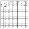
- FIG. 4 is a diagram showing an example of a code set when one field is composed of eight subfields.
- FIG. 5 is a diagram schematically showing an example of a circuit block constituting the plasma display device in one embodiment of the present invention.
- FIG. 6 is a diagram schematically showing an example of a circuit block constituting the image signal processing circuit of the plasma display device in one embodiment of the present invention.
- FIG. 7 is a diagram schematically showing an example of a circuit block constituting the G signal processing unit of the plasma display device in one embodiment of the present invention.
- FIG. 8A is a diagram showing an example of a base code set used in the plasma display device according to one embodiment of the present invention.
- FIG. 8B is a diagram showing another example of the base code set used in the plasma display device in one embodiment of the present invention.
- FIG. 9A is a diagram illustrating an example of a lighting pattern in which a charge loss phenomenon is likely to occur.
- FIG. 9B is a diagram illustrating an example of a lighting pattern in which a charge loss phenomenon may occur.
- FIG. 10A is a diagram showing an example of an intermediate code set generated in the intermediate code generation unit of the plasma display device in one embodiment of the present invention.
- FIG. 10B is a diagram showing another example of the intermediate code set generated in the intermediate code generation unit of the plasma display device in one embodiment of the present invention.
- FIG. 10C is a diagram showing another example of the intermediate code set generated in the intermediate code generation unit of the plasma display device in one embodiment of the present invention.
- FIG. 10D is a diagram showing another example of the intermediate code set generated in the intermediate code generation unit of the plasma display device in one embodiment of the present invention.
- FIG. 10E is a diagram showing another example of the intermediate code set generated in the intermediate code generation unit of the plasma display device in one embodiment of the present invention.
- FIG. 11A is a diagram showing an example of a dither pattern used in the plasma display device according to one embodiment of the present invention.
- FIG. 11A is a diagram showing an example of a dither pattern used in the plasma display device according to one embodiment of the present invention.
- FIG. 11B is a diagram showing another example of a dither pattern used in the plasma display device according to one embodiment of the present invention.
- FIG. 12 is a diagram showing the error diffusion coefficient of the error diffusion unit of the plasma display device in one embodiment of the present invention.
- FIG. 13 is a flowchart showing the operation of the image signal processing circuit of the plasma display device in one embodiment of the present invention.
- FIG. 14 is a diagram schematically showing an example of a region to which the second rule is applied and a region to which the second rule is not applied in the panel of the plasma display device according to one embodiment of the present invention.
- FIG. 1 is an exploded perspective view showing the structure of panel 10 used in the plasma display device according to one embodiment of the present invention.
- a plurality of display electrode pairs 14 each including a scanning electrode 12 and a sustaining electrode 13 are formed on a glass front substrate 11.
- a dielectric layer 15 is formed so as to cover the scan electrode 12 and the sustain electrode 13, and a protective layer 16 is formed on the dielectric layer 15.
- This protective layer 16 has been used as a panel material in order to lower the discharge start voltage in the discharge cell, and has a large secondary electron emission coefficient and durability when neon (Ne) and xenon (Xe) gas is sealed. It is made of a material mainly composed of magnesium oxide (MgO).
- the protective layer 16 may be composed of a single layer or may be composed of a plurality of layers. Moreover, the structure which particle
- a plurality of data electrodes 22 are formed on the rear substrate 21, a dielectric layer 23 is formed so as to cover the data electrodes 22, and a grid-like partition wall 24 is further formed thereon.
- a phosphor layer 25R that emits red (R)
- a phosphor layer 25G that emits green (G)
- a phosphor layer 25B that emits blue (B).
- the phosphor layer 25R, the phosphor layer 25G, and the phosphor layer 25B are collectively referred to as a phosphor layer 25.
- the front substrate 11 and the rear substrate 21 are arranged to face each other so that the display electrode pair 14 and the data electrode 22 intersect each other with a minute space therebetween, and a discharge space is provided in the gap between the front substrate 11 and the rear substrate 21.
- the outer peripheral part is sealed with sealing materials, such as glass frit.
- sealing materials such as glass frit.
- a mixed gas of neon and xenon is sealed in the discharge space as a discharge gas.
- the discharge space is partitioned into a plurality of sections by the barrier ribs 24, and discharge cells, which are light-emitting elements constituting the pixels, are formed at the intersections between the display electrode pairs 14 and the data electrodes 22.
- one pixel is composed of three consecutive discharge cells arranged in the direction in which the display electrode pair 14 extends.
- the three discharge cells are a discharge cell having a phosphor layer 25R and emitting red (R) (red discharge cell), and a discharge cell having a phosphor layer 25G and emitting green (G) (green). And a discharge cell having a phosphor layer 25B and emitting blue (B) light (blue discharge cell).
- the structure of the panel 10 is not limited to the above-described structure, and may be, for example, provided with a stripe-shaped partition wall.
- FIG. 2 is an electrode array diagram of panel 10 used in the plasma display device according to one embodiment of the present invention.
- the panel 10 includes n scan electrodes SC1 to SCn (scan electrode 12 in FIG. 1) extended in the horizontal direction (row direction and line direction) and n sustain electrodes SU1 to SUn (FIG. 1).
- the sustain electrodes 13) are arranged, and m data electrodes D1 to Dm (data electrodes 22 in FIG. 1) extending in the vertical direction (column direction) are arranged.
- m discharge cells are formed on one pair of display electrodes 14 and m / 3 pixels are formed.
- the plasma display device in the present embodiment drives the panel 10 by the subfield method.
- the subfield method one field of an image signal is divided into a plurality of subfields on the time axis, and a gradation weight is set for each subfield. Therefore, each field has a plurality of subfields having different gradation weights.
- Each subfield has an initialization period, an address period, and a sustain period. Based on the image signal, light emission / non-light emission of each discharge cell is controlled for each subfield. That is, a plurality of gradations based on the image signal are displayed on the panel 10 by combining the light-emitting subfield and the non-light-emitting subfield based on the image signal.
- an initializing operation is performed in which initializing discharge is generated in the discharge cells and wall charges necessary for the address discharge in the subsequent address period are formed on each electrode.
- Initialization operation includes “forced initialization operation” that forcibly generates an initializing discharge in all discharge cells regardless of the operation of the immediately preceding subfield and an addressing discharge that occurs in the addressing period of the immediately preceding subfield.
- the forced initializing operation the rising ramp waveform voltage and the falling ramp waveform voltage are applied to the scan electrode 12 to generate an initializing discharge in the discharge cell.
- the forced initializing operation is performed in all discharge cells in the initializing period of one subfield, and all the discharge cells are selected in the initializing period of the other subfield. Perform initialization.
- force initialization period the initialization period in which the forced initialization operation is performed
- subfield having the forced initialization period is referred to as “forced initialization subfield”.
- An initialization period for performing the selective initialization operation is referred to as a “selective initialization period”
- a subfield having the selective initialization period is referred to as a “selective initialization subfield”.
- subfield SF1 which is the first subfield of one field, is set as a forced initialization subfield
- the other subfields (subfields subsequent to subfield SF2) are set as selected initialization subfields.
- the present invention is not limited to the above-described subfields as subfields for forced initialization subfields and subfields for selective initialization subfields.
- the structure which switches a subfield structure based on an image signal etc. may be sufficient.
- a scan pulse is applied to the scan electrode 12 and an address pulse is selectively applied to the data electrode 22 to selectively generate an address discharge in the discharge cells to emit light. Then, an address operation is performed to form wall charges in the discharge cells for generating a sustain discharge in the subsequent sustain period.
- sustain pulses of the number obtained by multiplying the gradation weight set in each subfield by a predetermined proportional constant are alternately applied to the scan electrode 12 and the sustain electrode 13 to generate an address discharge in the immediately preceding address period.
- a sustain discharge is generated in the discharged discharge cell, and a sustain operation for emitting light from the discharge cell is performed.
- This proportionality constant is a luminance multiple.
- the gradation weight represents the ratio of the magnitude of the luminance displayed in each subfield, and the number of sustain pulses corresponding to the gradation weight is generated in the sustain period in each subfield. Therefore, for example, the subfield with the gradation weight “8” emits light with a luminance about eight times that of the subfield with the gradation weight “1”, and about four times as high as the subfield with the gradation weight “2”. Emits light. Therefore, for example, if the subfield with the gradation weight “8” and the subfield with the gradation weight “2” are emitted, the discharge cell can emit light with a luminance corresponding to the gradation value “10”.
- each discharge cell emits light with various gradation values by selectively emitting light in each subfield by controlling light emission / non-light emission of each discharge cell for each subfield in a combination according to the image signal. That is, a gradation value corresponding to an image signal can be displayed on each discharge cell, and an image based on the image signal can be displayed on the panel 10.
- one field is composed of eight subfields (subfield SF1, subfield SF2,..., Subfield SF8), and each subfield from subfield SF1 to subfield SF8 has (1 2, 3, 5, 8, 13, 21, 34) will be described.
- the gradation weight is set in each subfield so that the gradation weight becomes larger in the later subfield.
- a red image signal, a green image signal, and a blue image signal can be displayed with a plurality of gradations, respectively.
- the red image signal is abbreviated as “R signal”
- the green image signal is abbreviated as “G signal”
- the blue image signal is abbreviated as “B signal”.
- the number of subfields constituting one field and the luminance weight of each subfield are not limited to the above values.
- the structure which switches a subfield structure based on an image signal etc. may be sufficient.
- one pixel includes three consecutive discharge cells arranged in the direction in which the display electrode pair 14 extends, that is, a red discharge cell, a green discharge cell, and a blue discharge.
- a red discharge cell is also referred to as a “red pixel”, a green discharge cell as a “green pixel”, and a blue discharge cell as a “blue pixel”.
- FIG. 3 is a diagram schematically showing drive voltage waveforms applied to the respective electrodes of panel 10 used in the plasma display device according to one embodiment of the present invention.
- FIG. 3 shows data electrode D1 to data electrode Dm, scan electrode SC1 that performs the address operation first in the address period, scan electrode SCn that performs the address operation last in the address period (for example, scan electrode SC1080), sustain electrode SU1 to The drive voltage waveform applied to each of the sustain electrodes SUn is shown.
- Scan electrode SCi, sustain electrode SUi, and data electrode Dk in the following represent electrodes selected based on image data (data indicating light emission / non-light emission for each subfield) from among the electrodes.
- FIG. 3 shows a subfield SF1 that is a forced initialization subfield, and a subfield SF2 and a subfield SF3 that are selective initialization subfields.
- the subfield SF1, the subfield SF2, and the subfield SF3 have different waveform shapes of the drive voltage applied to the scan electrode 12 in the initialization period.
- each subfield except subfield SF1 is a selective initialization subfield, and substantially the same drive voltage waveform in each period except the number of sustain pulses. Is generated.
- the voltage 0 (V) is applied to the data electrode D1 to the data electrode Dm and the sustain electrode SU1 to the sustain electrode SUn.
- a voltage Vi1 is applied to scan electrode SC1 through scan electrode SCn after voltage 0 (V) is applied, and a ramp waveform voltage that gradually rises from voltage Vi1 to voltage Vi2 (hereinafter referred to as an “upward ramp waveform voltage”). ) Is applied.
- voltage Vi1 is set to a voltage lower than the discharge start voltage for sustain electrode SU1 to sustain electrode SUn
- voltage Vi2 is set to a voltage exceeding the discharge start voltage for sustain electrode SU1 to sustain electrode SUn.
- the wall voltage on the electrode represents a voltage generated by wall charges accumulated on the dielectric layer covering the electrode, the protective layer, the phosphor layer, and the like.
- the positive voltage Ve is applied to the sustain electrodes SU1 to SUn, and the voltage 0 (V) is applied to the data electrodes D1 to Dm.
- a scan waveform SC1 to scan electrode SCn are applied with a ramp waveform voltage that gently falls from voltage Vi3 to negative voltage Vi4 (hereinafter referred to as “down ramp waveform voltage”).
- Voltage Vi3 is set to a voltage lower than the discharge start voltage with respect to sustain electrode SU1 through sustain electrode SUn
- voltage Vi4 is set to a voltage exceeding the discharge start voltage with respect to sustain electrode SU1 through sustain electrode SUn.
- the above voltage waveform is a forced initializing waveform that generates an initializing discharge in the discharge cell regardless of the operation of the immediately preceding subfield.
- the operation for applying the forced initialization waveform to the scan electrode 12 is the forced initialization operation.
- the forced initialization operation in the initialization period Ti1 of the forced initialization subfield ends.
- initializing discharge is forcibly generated in all the discharge cells in the image display area of the panel 10.
- voltage Ve is applied to sustain electrode SU1 through sustain electrode SUn
- voltage 0 (V) is applied to data electrode D1 through data electrode Dm
- scan electrode SC1 through scan electrode SCn are applied. Applies a voltage Vc.
- a negative scan pulse having a negative voltage Va is applied to the first (first row) scan electrode SC1 in terms of arrangement.
- a positive address pulse of a positive voltage Vd is applied to the data electrode Dk of the discharge cell that should emit light in the first row of the data electrodes D1 to Dm.
- sustain electrode SU1 since voltage Ve is applied to sustain electrode SU1 through sustain electrode SUn, sustain electrode SU1 in a region intersecting data electrode Dk is induced by a discharge generated between data electrode Dk and scan electrode SC1. Discharge also occurs between scan electrode SC1 and scan electrode SC1. Thus, address discharge is generated in the discharge cells (discharge cells to emit light) to which the scan pulse voltage Va and the address pulse voltage Vd are simultaneously applied.
- a positive wall voltage is accumulated on the scan electrode SC1
- a negative wall voltage is accumulated on the sustain electrode SU1
- a negative wall voltage is also accumulated on the data electrode Dk.
- the address operation in the discharge cells in the first row is completed.
- the discharge cell having the data electrode Dh to which the address pulse is not applied the data electrode Dh is the data electrode D1 to the data electrode Dm excluding the data electrode Dk
- the intersection of the data electrode Dh and the scan electrode SC1 Since the voltage of the portion does not exceed the discharge start voltage, the address discharge does not occur, and the wall voltage after the end of the initialization period Ti1 is maintained.
- a scan pulse of the voltage Va is applied to the second (second row) scan electrode SC2 from the top, and the voltage Vd is applied to the data electrode Dk corresponding to the discharge cell to emit light in the second row. Apply the write pulse.
- address discharge occurs in the discharge cells in the second row to which the scan pulse and address pulse are simultaneously applied.
- the address operation in the discharge cells in the second row is performed.
- voltage Ve applied to sustain electrode SU1 through sustain electrode SUn in the second half of initialization period Ti1 and voltage Ve applied to sustain electrode SU1 through sustain electrode SUn in address period Tw1 may have different voltage values. .
- the voltage 0 (V) is applied to the sustain electrodes SU1 to SUn. Then, sustain pulse of positive voltage Vs is applied to scan electrode SC1 through scan electrode SCn.
- the voltage difference between the scan electrode SCi and the sustain electrode SUi exceeds the discharge start voltage, and is maintained between the scan electrode SCi and the sustain electrode SUi. Discharge occurs. Then, the phosphor layer 25 of the discharge cell in which the sustain discharge has occurred emits light by the ultraviolet rays generated by the sustain discharge, and the discharge cell is turned on.
- a negative wall voltage is accumulated on scan electrode SCi, and a positive wall voltage is accumulated on sustain electrode SUi. Furthermore, a positive wall voltage is also accumulated on the data electrode Dk.
- the sustain discharge does not occur in the discharge cells in which the address discharge has not occurred in the address period Tw1, and the wall voltage after the end of the initialization period Ti1 is maintained.
- the sustain pulses of the number obtained by multiplying the gradation weight by a predetermined luminance multiple are alternately applied to scan electrode SC1 through scan electrode SCn and sustain electrode SU1 through sustain electrode SUn.
- the discharge cells that have generated the address discharge in the address period generate the sustain discharges the number of times corresponding to the gradation weight, and emit light with the luminance corresponding to the gradation weight.
- scan electrode SC1 to scan are performed while voltage 0 (V) is applied to sustain electrode SU1 to sustain electrode SUn and data electrode D1 to data electrode Dm.
- An upward ramp waveform voltage that gradually rises from voltage 0 (V) to voltage Vr is applied to electrode SCn.
- the sustain of the discharge cell that has generated the sustain discharge is maintained while the rising ramp waveform voltage applied to scan electrode SC1 through scan electrode SCn exceeds the discharge start voltage.
- a weak discharge (erase discharge) is continuously generated between the electrode SUi and the scan electrode SCi.
- the charged particles generated by this weak discharge are accumulated as wall charges on the sustain electrode SUi and the scan electrode SCi so as to reduce the voltage difference between the sustain electrode SUi and the scan electrode SCi.
- the wall voltage on scan electrode SCi and the wall voltage on sustain electrode SUi are weakened while the positive wall voltage on data electrode Dk remains.
- unnecessary wall charges in the discharge cell are erased.
- the voltage 0 (V) is applied to the data electrodes D1 to Dm, and the positive voltage Ve is applied to the sustain electrodes SU1 to SUn.
- Scan electrode SC1 to scan electrode SCn decrease from a voltage lower than the discharge start voltage (for example, voltage 0 (V)) toward negative voltage Vi4 at the same gradient as the downward ramp waveform voltage generated in initialization period Ti1. Apply a downward ramp waveform voltage.
- the voltage Vi4 is set to a voltage exceeding the discharge start voltage.
- the negative wall voltage on scan electrode SCi and the positive wall voltage on sustain electrode SUi are weakened.
- an excessive portion of the positive wall voltage on the data electrode Dk is discharged.
- the wall voltage in the discharge cell is adjusted to a wall voltage suitable for the address operation in the address period Tw2.
- the voltage waveform described above is a selective initialization waveform in which an initializing discharge is selectively generated in a discharge cell that has performed an address operation in the address period (here, address period Tw1) of the immediately preceding subfield.
- the operation of applying the selective initialization waveform to the scan electrode 12 is the selective initialization operation.
- the same drive voltage waveform as that in the address period Tw1 of the subfield SF1 is applied to each electrode.
- the number of sustain pulses corresponding to the gradation weights are alternately applied to the scan electrodes SC1 to SCn and the sustain electrodes SU1 to SUn.
- each subfield after subfield SF3 the same drive voltage waveform as in subfield SF2 is applied to each electrode except for the number of sustain pulses generated in the sustain period.
- Voltage Vc ⁇ 60 (V)
- voltage Va ⁇ 200 (V)
- voltage Vs 200 (V)
- voltage Vr 200 (V)
- voltage Ve 130 (V)
- voltage Vd 70 (V)
- the gradient of the rising ramp waveform voltage generated in the initialization period Ti1 is about 1.3 V / ⁇ sec
- the gradient of the rising ramp waveform voltage generated in each sustain period is about 10 V / ⁇ sec.
- the gradient of the generated downward ramp waveform voltage is about ⁇ 1.5 V / ⁇ sec.
- the specific numerical values such as the voltage value and the gradient described above are merely examples, and the present invention is not limited to the numerical values described above for each voltage value and the gradient.
- Each voltage value, gradient, and the like are preferably set optimally based on the discharge characteristics of the panel and the specifications of the plasma display device.
- subfield SF1 is a forced initialization subfield for performing a forced initialization operation
- other subfields are a selective initialization subfield for performing a selective initialization operation
- the present invention is not limited to this configuration.
- the subfield SF1 may be a selective initialization subfield and other subfields may be forced initialization subfields, or a plurality of subfields may be forced initialization subfields.
- one field is composed of a plurality of subfields in which gradation weights are determined in advance. Then, by combining a subfield that is lit (lighting subfield) and a subfield that is not lit (non-lighting subfield), each discharge cell emits light with a light emission luminance corresponding to the magnitude of the gradation value based on the image signal. .
- subfield code a combination of a lighting subfield and a non-lighting subfield
- code set a set of a plurality of subfield codes
- the subfield code is composed of the same number of bit signals as each subfield constituting one field.
- Each bit signal is either “1” or “0”, “1” indicates that the subfield is a lighting subfield, and “0” indicates that the subfield is a non-lighting subfield.
- the subfield codes are arranged in the order of subfield SF1, subfield SF2, subfield SF3,... From the left.
- the subfield code “11101000” indicates that the subfield SF1, the subfield SF2, the subfield SF3, and the subfield SF5 are lighting subfields, and the other subfields are non-lighting subfields.
- a subfield code is selected from a plurality of subfield codes constituting a code set according to a gradation value. Then, light emission / non-light emission of each subfield is controlled based on the subfield code, and the discharge cell is caused to emit light with a luminance corresponding to the magnitude of the gradation value, and an image is displayed on the panel 10.
- the gradation value when displaying black (the gradation value when no sustain discharge occurs) is assumed to be “0”.
- a gradation value corresponding to the gradation weight “N” is expressed as a gradation value “N”.
- the gradation value displayed by the discharge cells that emit light only in the subfield SF1 having the gradation weight “1” is the gradation value “1”.
- FIG. 4 is a diagram showing an example of a code set when one field is composed of eight subfields.
- the numerical value shown immediately below the notation indicating each subfield represents the gradation weight of each subfield.
- FIG. 4 includes eight subfields SF1 to SF8 in one field, and each subfield is “1”, “2”, “3”, “5”, “8”, respectively. ”,“ 13 ”,“ 21 ”, and“ 34 ”indicate code sets having gradation weights.
- the light emitting subfield is indicated by “1”
- the non-light emitting subfield is indicated by a blank
- the leftmost column indicates the gradation value to be displayed in each subfield code.
- the subfield code corresponding to the gradation value “2” is “01000000”.
- subfield code data 0 or 1 is arranged in the order of subfield SF1, subfield SF2, subfield SF3, subfield SF4, subfield SF5, subfield SF6, subfield SF7, and subfield SF8 from the left.
- binary numerical values shown as subfield codes are arranged in the order of subfield SF1, subfield SF2, subfield SF3,.
- the subfield code corresponding to the gradation value “14” is “11101000”. Accordingly, in the discharge cell displaying the gradation value “14”, the subfield SF1, the subfield SF2, the subfield SF3, and the subfield SF5 emit light.
- FIG. 5 is a diagram schematically showing an example of a circuit block constituting the plasma display device 30 in one embodiment of the present invention.
- the plasma display device 30 includes a panel 10 and a drive circuit that drives the panel 10.
- the drive circuit includes an image signal processing circuit 31, a data electrode drive circuit 32, a scan electrode drive circuit 33, a sustain electrode drive circuit 34, a timing generation circuit 35, and a power supply circuit (not shown) that supplies necessary power to each circuit block. It has.
- the image signals input to the image signal processing circuit 31 are a red image signal (R signal), a green image signal (G signal), and a blue image signal (B signal). Based on the red image signal, the green image signal, and the blue image signal, the image signal processing circuit 31 sets each gradation value of red, green, and blue (a gradation value expressed by one field) to each discharge cell. To do.
- the input image signal includes a luminance signal (Y signal) and a saturation signal (C signal, or RY signal and BY signal, or u signal and v signal, etc.).
- a red image signal, a green image signal, and a blue image signal are calculated based on the luminance signal and the saturation signal, and then, each gradation value of red, green, and blue is set in each discharge cell.
- the image signal processing circuit 31 uses the red, green, and blue gradation values set for each discharge cell as a subfield code (light emission / non-light emission for each subfield). ", Data corresponding to" 0 "), and the subfield code is output as a display code. That is, the image signal processing circuit 31 converts the red image signal, the green image signal, and the blue image signal into a red display code, a green display code, and a blue display code and outputs the converted signals.
- the red display code is referred to as “R display code”
- the green display code is referred to as “G display code”
- the blue display code is referred to as “B display code”.
- the image signal processing circuit 31 does not convert an image signal into a subfield code using a conversion table, but converts the image signal into a subfield code by a logical operation. Details of this will be described later.
- the timing generation circuit 35 generates various timing signals for controlling the operation of each circuit block based on the horizontal synchronization signal and the vertical synchronization signal.
- the generated timing signal is supplied to each circuit block (data electrode drive circuit 32, scan electrode drive circuit 33, sustain electrode drive circuit 34, image signal processing circuit 31, etc.).
- Scan electrode drive circuit 33 includes a ramp waveform generation unit, a sustain pulse generation unit, and a scan pulse generation unit (not shown in FIG. 5), and generates a drive voltage waveform based on a timing signal supplied from timing generation circuit 35. Then, the voltage is applied to each of scan electrode SC1 to scan electrode SCn.
- the ramp waveform generator generates a forced initialization waveform and a selective initialization waveform to be applied to scan electrode SC1 through scan electrode SCn during the initialization period based on the timing signal.
- the sustain pulse generator generates a sustain pulse to be applied to scan electrode SC1 through scan electrode SCn during the sustain period based on the timing signal.
- the scan pulse generator includes a plurality of scan electrode drive ICs (scan ICs), and generates scan pulses to be applied to scan electrode SC1 through scan electrode SCn during the address period based on the timing signal.
- Sustain electrode drive circuit 34 includes a sustain pulse generation unit and a circuit (not shown in FIG. 5) for generating voltage Ve, and generates and maintains a drive voltage waveform based on the timing signal supplied from timing generation circuit 35.
- the voltage is applied to each of electrode SU1 through sustain electrode SUn.
- a sustain pulse is generated based on the timing signal and applied to sustain electrode SU1 through sustain electrode SUn.
- voltage Ve is generated based on the timing signal and applied to sustain electrode SU1 through sustain electrode SUn.
- the data electrode driving circuit 32 is based on each color display code (R display code, G display code, B display code) output from the image signal processing circuit 31 and the timing signal supplied from the timing generation circuit 35. Address pulses corresponding to D1 to data electrode Dm are generated. Then, the data electrode driving circuit 32 applies an address pulse (address pulse voltage Vd or 0 (V)) to each of the data electrodes D1 to Dm in the address period.
- an address pulse address pulse voltage Vd or 0 (V)
- FIG. 6 is a diagram schematically showing an example of a circuit block constituting the image signal processing circuit 31 of the plasma display device 30 in one embodiment of the present invention.
- the image signal processing circuit 31 includes an image signal processing unit corresponding to a red image signal, an image signal processing unit corresponding to a green image signal, and an image signal processing unit corresponding to a blue image signal.
- the image signal processing unit corresponding to the red image signal will be referred to as “R signal processing unit 40R”
- the image signal processing unit corresponding to the green image signal will be referred to as “G signal processing unit 40G”
- the blue image signal will be described.
- the image signal processing unit corresponding to is described as “B signal processing unit 40B”. That is, the R signal processing unit 40R is a “red image signal processing unit”, the G signal processing unit 40G is a “green image signal processing unit”, and the B signal processing unit 40B is a “blue image signal processing unit”. It is.
- the R signal processing unit 40R generates a red display code (R display code) based on the red image signal (R signal), and outputs the R display code.
- the G signal processing unit 40G generates a green display code (G display code) based on the green image signal (G signal), and outputs the G display code.
- G display code green display code
- the B signal processing unit 40B generates a blue display code (B display code) based on the blue image signal (B signal) and outputs the B display code.
- the R signal processing unit 40R includes an attribute detection unit 41R, a base code generation unit 50R, a rule generation unit 61R, an upper / lower code generation unit 70R, and a display code selection unit 80R.
- the G signal processing unit 40G includes an attribute detection unit 41G, a base code generation unit 50G, a rule generation unit 61G, a rule addition unit 62G, an upper and lower code generation unit 70G, and a display code selection unit 80G.
- the B signal processing unit 40B includes an attribute detection unit 41B, a base code generation unit 50B, a rule generation unit 61B, an upper and lower code generation unit 70B, and a display code selection unit 80B.
- the R signal processing unit 40R and the B signal processing unit 40B have the same configuration.
- the G signal processing unit 40G has a configuration in which a rule adding unit 62G is added to the configuration of the R signal processing unit 40R (or B signal processing unit 40B).
- the R signal processing unit 40R and the B signal processing unit 40B are configured by removing the rule adding unit 62G from the G signal processing unit 40G, and thus detailed description thereof is omitted.
- FIG. 7 is a diagram schematically showing an example of a circuit block constituting the G signal processing unit 40G of the plasma display device 30 in one embodiment of the present invention.
- the G signal processing unit 40G includes an attribute detection unit 41G, a base code generation unit 50G, a rule generation unit 61G, a rule addition unit 62G, an upper and lower code generation unit 70G, and a display code selection unit 80G.
- the attribute detection unit 41G specifies the relationship between the G signal and the position of the green pixel that displays the G signal. Whether the green pixel is in the moving image area by time differentiation of the G signal corresponding to the green pixel (detecting a change in the G signal between the current field and the next field with respect to the same green pixel). Detecting whether it is in the still image area. In addition, a change in brightness is detected by spatial differentiation of the G signal (for a green pixel, a change in the G signal is detected between adjacent green pixels), and whether or not the green pixel corresponds to the contour of the image. Perform detection. Then, those detection results are output as the attribute of the G signal corresponding to the green pixel.
- the attribute detection unit 41R performs the same operation as the attribute detection unit 41G and outputs the attribute of the R signal.
- the attribute detection unit 41B performs the same operation as the attribute detection unit 41G and outputs the attribute of the B signal.
- a subfield code that is basic in subsequent signal processing is referred to as a “basic code”, and a code set including the base code is referred to as a “basic code set”.
- the base code is a subfield code generated by lighting one by one or two in order from the subfield having the smallest gradation weight. Therefore, the base code is a subfield code in which a subfield having the largest gradation weight among the subfields to emit light and all subfields having a gradation weight smaller than that subfield emit light.
- the base code generation unit 50G selects the tone value of the G signal input to the image signal processing circuit 31 (hereinafter referred to as “G input tone” or simply “input” from the base code set including a plurality of base codes. “G gradation base code” is selected based on “gradation”.
- the G upper tone base code is a base code having a tone value larger than the G input tone and having a tone value closest to the G input tone. Therefore, in the G upper gradation base code, the subfield having the largest gradation weight among the lighting subfields and all subfields having the gradation weight smaller than that subfield are the lighting subfields.
- the base code generation unit 50G selects a base code having a gray scale value that is larger than the G input gray scale and closest to the G input gray scale, and outputs it as the G upper gray scale base code.
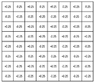
- FIG. 8A is a diagram showing an example of a base code set used in the plasma display device 30 according to one embodiment of the present invention.
- FIG. 8B is a diagram showing another example of the base code set used in the plasma display device 30 according to the embodiment of the present invention.
- the light-emitting subfield is “1”
- the non-light-emitting subfield is blank
- the second column from the left is the subfield code (base code).
- the numerical value written immediately below the notation indicating each subfield in each base code set represents the gradation weight of each subfield.
- FIG. 8A shows an example of a base code set often used in the NTSC standard.
- one field is composed of eight subfields, and each subfield is “1”, “2”, “3”, “5”, “ It has gradation weights of “8”, “13”, “21”, and “34”.
- the first subfield (subfield SF1) of one field is set to the subfield having the smallest gradation weight, and thereafter, the subfields are arranged so that the gradation weight is sequentially increased. . And it is set as a lighting subfield one by one in an order from the subfield with the smallest gradation weight. Therefore, the number of base codes included in this base code set is (the number of subfields constituting one field + 1). For example, in the example of the base code set shown in FIG. 8A, the number of base codes is nine.
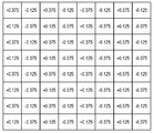
- FIG. 8B shows an example of a base code set often used in the PAL standard.
- one field includes 12 subfields, and each subfield is “1”, “2”, “4”, “9”, “9” in order from the subfield SF1. It has gradation weights of “18”, “36”, “65”, “5”, “7”, “15”, “33”, “60”.
- the base code set shown in FIG. 8B has two subfield groups.
- the first subfield group is composed of subfields SF1 to SF7, and the second subfield group is composed of subfields SF8 to SF12.
- Each subfield group has the first subfield of each subfield group (subfield SF1 and subfield SF8 in the example shown in FIG. 8B) as the subfield having the smallest gradation weight in each subfield group. Thereafter, the subfields are arranged so that the gradation weights are sequentially increased. In each subfield group, one or two lighting subfields are set in order from the subfield having the smallest gradation weight. Therefore, the number of base codes included in this base code set is equal to or less than (the number of subfields constituting one field + 1). For example, in the example of the base code set shown in FIG. 8B, the number of base codes is 10.
- the plasma display device 30 generates a new code set based on the base code set as described above, and uses the code set to input gradation (R input gradation, G input gradation, and B input). Each input gradation of gradation) is converted into a subfield code.
- the base code generation unit 50G includes a base code storage unit 52G and a base code selection unit 54G.
- the base code storage unit 52G stores a base code set and each gradation value of a plurality of base codes constituting the base code set. Each base code and each gradation value of the base code are associated with each other and stored in the base code storage unit 52G.
- the base code selection unit 54G compares each tone value of the base code constituting the base code set with the G input tone. Then, a base code having a gradation value larger than the G input gradation and closest to the G input gradation is selected. Then, the selected base code is output as an upper G tone base code.
- the base code generation unit 50R includes a base code storage unit 52R and a base code selection unit 54R, similar to the base code generation unit 50G. Then, a base code having a gradation value larger than the R input gradation and closest to the R input gradation is selected, and the selected base code is output as an R upper gradation base code.
- the base code generation unit 50B includes a base code storage unit 52B and a base code selection unit 54B, similarly to the base code generation unit 50G. Then, a base code having a gradation value larger than the B input gradation and closest to the B input gradation is selected, and the selected base code is output as the B upper gradation base code.
- the rule generation unit 61G Based on the G signal input to the image signal processing circuit 31, by changing the lighting subfield in the G upper gradation base code to the non-lighting subfield, a new code not included in the base code set is obtained. Generate subfield codes.
- the rule generation unit 61G generates a first rule relating to the G signal in order to generate this new subfield code.
- the first rule regarding the G signal is also referred to as a “G rule”.
- the rule generation unit 61G increases the number of subfield codes used for image display based on the attribute attached to the G signal detected by the attribute detection unit 41G and the G selected by the base code generation unit 50G.
- a G rule for changing the lighting subfield in the upper gradation base code to the non-lighting subfield is generated.
- the G rule generated by the rule generation unit 61G in the present embodiment defines the law for changing the lighting subfield in the G upper gradation base code to the non-lighting subfield.
- the rule generated by the rule generation unit 61G restricts subfields to be changed from lighting to non-lighting in the G upper gradation base code. This is because the gradation value of the base code in which the gradation value of the new subfield code created by changing the lighting subfield to the non-lighting subfield in the G upper gradation base code is smaller than the G upper gradation base code. This is so as not to fall below the value.
- the G rule is generated so that the subfield code generated based on the rule has the next gradation value.
- the “G lower gradation base code” is a base code having a gradation value that is equal to or lower than the G input gradation and closest to the G input gradation.
- the G rule generated by the rule generation unit 61G includes one or more of the following three rules. 1) A rule for setting the first subfield to be changed from the lighting subfield to the non-lighting subfield. 2) A rule for setting the second subfield to be changed from the lighting subfield to the non-lighting subfield. 3) A rule for setting a sub-field that prohibits non-lighting.
- the rule generation unit 61R uses a base code generation unit based on the attribute attached to the R signal detected by the attribute detection unit 41R in order to increase the number of subfield codes used for image display.
- An R rule (first rule regarding the R signal) for changing the lighting subfield in the R upper gradation base code selected in 50R to the non-lighting subfield is generated.
- the rule generation unit 61B uses a base code generation unit based on attributes associated with the B signal detected by the attribute detection unit 41B in order to increase the number of subfield codes used for image display.
- a B rule (first rule regarding the B signal) for changing the lighting subfield in the B upper gradation base code selected in 50B to the non-lighting subfield is generated.
- the rule adding unit 62G generates a second rule.
- the second rule is a subfield that occurs after a predetermined subfield in a field with respect to a predetermined subfield in which two adjacent discharge cells on both sides of a discharge cell of a predetermined color emit light together.
- This is a rule for generating a display code for a discharge cell of a predetermined color so that a predetermined subfield emits light when the discharge cell of the predetermined color emits light.
- the discharge cell having the predetermined color is a discharge cell that emits green light. Therefore, according to the second rule, in the G display code for green pixels, R for adjacent red pixels is determined for each subfield that occurs temporally before the subfield with the highest luminance weight among the subfields to be lit. Based on the display code and the B display code for the adjacent blue pixel, this is a rule for defining subfields that are prohibited from being unlit.
- the second rule is that a subfield that occurs later in time than a subfield in a subfield in which both red and blue pixels adjacent to a green pixel are lit in one field.
- the rule is that when a green pixel is turned on, the subfield is prohibited from being turned off.
- This second rule is for stabilizing the address discharge by suppressing the charge loss phenomenon while preventing the image display quality in the plasma display device 30 from deteriorating.
- the rule adding unit 62G includes an R upper gradation base code generated by the base code generation unit 50R of the R signal processing unit 40R, an G upper gradation base code generated by the base code generation unit 50G of the G signal processing unit 40G, and The B upper gradation base code generated by the base code generation unit 50B of the B signal processing unit 40B is input.
- the R upper gradation base code is generated for the red pixel adjacent to the green pixel of interest.
- the B upper gradation base code is generated for a blue pixel adjacent to the green pixel of interest.
- the pixel of interest is a pixel that is a target of calculation of a gradation value at that time.
- the green pixel of interest is the green discharge cell of the pixel of interest
- the red pixel of interest is the red discharge cell of the pixel of interest
- the blue pixel of interest is the pixel of interest. This is the blue discharge cell in the pixel.
- one pixel is composed of three discharge cells arranged in the order of a red discharge cell, a green discharge cell, and a blue discharge cell. Therefore, in one pixel, the discharge cells adjacent to the green discharge cell are a red discharge cell and a blue discharge cell. Therefore, the above R upper gradation base code, G upper gradation base code, and B upper gradation base code are the R upper gradation base code, G upper gradation base code, and B upper gradation generated in one pixel. This is the base code.
- the rule adding unit 62G generates a second rule to be used in the subsequent upper and lower code generation unit 70G from the R upper gradation base code, the G upper gradation base code, and the B upper gradation base code.
- the second rule defines a subfield that prohibits changing the lighting subfield to the non-lighting subfield in the upper and lower code generation unit 70G in the subsequent stage.
- the rule adding unit 62G performs an AND operation on the R upper gradation base code and the B upper gradation base code.
- the rule adding unit 62G replaces the bit signal corresponding to the subfield having the largest gradation weight among the lighting subfields with “0” in the G upper gradation base code in the green pixel of interest, and further increases the level.
- a subfield code is generated in which the bit signal corresponding to the subfield having the key weight remains “0”.
- the rule adding unit 62G outputs the subfield code resulting from the logical product operation as the second rule.
- the G upper gradation base code is “11100000”
- the R upper gradation base code is “11111000”
- the B upper gradation base code is “11111100”.
- the rule adding unit 62G performs a logical product operation of the R upper gradation base code “11111000” and the B upper gradation base code “11111100”.
- the subfield code resulting from the logical product operation is “11111000”.
- the rule adding unit 62G generates a subfield code “11000000” in which the bit signal of the subfield SF3 is replaced from “1” to “0”.
- the rule adding unit 62G performs an AND operation on the subfield code “11111000” as a result of the above AND operation and the subfield code “11000000”.
- the result of the logical product operation is “11000000”.
- the rule adding unit 62G outputs the subfield code “11000000” as the second rule to the upper and lower code generation unit 70G in the subsequent stage.
- the subfields in which the bit signal is “1” are the subfield SF1 and the subfield SF2. Therefore, the second rule at this time is “inhibition of making subfield SF1 and subfield SF2 non-lighting subfields”.
- the rule adding unit 62G generates the second rule from the R upper gradation base code, the G upper gradation base code, and the B upper gradation base code.
- the G upper gradation base code is “11111100”
- the R upper gradation basic code is “11111100”
- the B upper gradation base code is “11110000”.
- the rule adding unit 62G performs a logical AND operation on the R upper gradation base code “11111100” and the B upper gradation base code “11110000”.
- the subfield code resulting from the logical product operation is “11110000”.
- the subfield having the largest gradation weight is the subfield SF6. Accordingly, the rule adding unit 62G generates a subfield code “11111000” in which the bit signal of the subfield SF6 is replaced from “1” to “0”.
- the rule adding unit 62G performs an AND operation on the subfield code “11110000” as a result of the above AND operation and the subfield code “11111000”.
- the result of the logical product operation is “11110000”.
- the rule adding unit 62G outputs the subfield code “11110000” as the second rule to the upper and lower code generation unit 70G in the subsequent stage.
- the subfields in which the bit signal is “1” are the subfield SF1 to the subfield SF4. Therefore, the second rule at this time is “prohibit each subfield of subfield SF1 to subfield SF4 from being a non-lighting subfield”.
- the rule adding unit 62G generates the second rule used by the upper / lower code generation unit 70G in the subsequent stage from the R upper tone base code, the G upper tone base code, and the B upper tone base code.
- the second rule is generated for the purpose of stabilizing the wall charge by suppressing the fluctuation of the wall charge caused by the charge loss phenomenon and the like, and stabilizing the address discharge.
- the wall charge accumulated in the discharge cell is adjusted to a wall voltage suitable for address discharge by initialization discharge.
- initializing discharge is generated in all the discharge cells. Therefore, the address discharge can be stably generated in the address period Tw1 of the subfield SF1.
- the initializing discharge is generated only in the discharge cells that have generated the sustaining discharge in the immediately preceding subfield. Therefore, in the discharge cell in which the initializing discharge has occurred, the address discharge can be stably generated during the address period of the subfield.
- the initializing discharge does not occur in the discharge cell in which no sustain discharge has occurred in the immediately preceding subfield.
- the wall charge is reduced as compared with the discharge cell that generates the initialization discharge. Therefore, the address discharge tends to become unstable when the charge loss phenomenon occurs.
- Charge loss phenomenon is a phenomenon in which wall charges in a discharge cell are reduced by occurrence of address discharge or sustain discharge in an adjacent discharge cell.
- green phosphors tend to be negatively charged. For this reason, the green discharge cell is more likely to cause a charge loss phenomenon than the red discharge cell and the blue discharge cell.
- FIG. 9A is a diagram showing an example of a lighting pattern in which a charge loss phenomenon is likely to occur.
- FIG. 9A shows the subfield that emits light as “1” and the non-light-emitting subfield as blank.
- the red discharge cell is referred to as “R cell”, the green discharge cell as “G cell”, and the blue discharge cell as “B cell”.
- the G display code is “11011100”
- the R display code is “11111100”
- the B display code is It is assumed that “11110000”.
- the G cell is not lit in the subfield SF3. However, both the R cell adjacent to the G cell and the B cell adjacent to the G cell are lit. In addition, the G cell is lit in the subfield SF4. That is, in the example shown in FIG. 9A, the predetermined subfield is the subfield SF3.
- the address discharge may become unstable in the subfield SF4.
- the address discharge may not occur in the subfields subsequent to the subfield SF4.
- the subfield SF3 may be changed from non-lighting to lighting.
- the R upper gradation base code is “1” in one pixel including the R cell, the G cell, and the B cell, and the B upper gradation.
- the G cell is prohibited from being unlit. This is the second rule.
- the subfield SF3 of the G cell is changed from non-lighting to lighting. Therefore, the address discharge can be stably generated in the subfield SF4 of the G cell.
- FIG. 9B is a diagram illustrating an example of a lighting pattern in which a charge loss phenomenon may occur.
- FIG. 9B shows the subfield that emits light as “1” and the non-light-emitting subfield as blank.
- the red discharge cell is referred to as “R cell”, the green discharge cell as “G cell”, and the blue discharge cell as “B cell”.
- the G display code is “11110100”
- the R display code is “11111100”
- the B display code is It is assumed that “11110000”.
- the G cell and the B cell are not lit in the subfield SF5.
- the R cell adjacent to the G cell is lit.
- the G cell is lit in the subfield SF6.
- the R upper gradation base code is “1” and the B upper gradation base code is “1” in one pixel including the R cell, the G cell, and the B cell.
- the G cell is not prohibited from being unlit. Similarly, it is not prohibited to turn off the G cell even in a subfield in which the R upper gradation base code is “0” and the B upper gradation base code is “1”.
- the present invention is not limited to this configuration.
- the G cell may be prohibited from being unlit in the subfield where the R upper gradation base code is “1” and the B upper gradation base code is “0”.
- the G cell may be prohibited from being turned off in the subfield in which the R upper gradation base code is “0” and the B upper gradation base code is “1”.
- the rule adding unit 62G may perform a logical sum operation instead of the logical product operation with the R upper gradation base code and the B upper gradation base code. .
- the upper and lower code generation unit 70G applies the G rule generated by the rule generation unit 61G and the second rule generated by the rule addition unit 62G to the G upper gradation base code output from the base code generation unit 50G, A G upper gradation code and a G lower gradation code are generated.
- the G upper gradation code is a gradation value that is larger than the G input gradation and closest to the G input gradation among subfield codes that can be newly generated based on the G rule and the second rule. It is a subfield code having.
- the G lower gradation code is a gradation value that is lower than the G input gradation and closest to the G input gradation among the subfield codes that can be newly generated based on the G rule and the second rule. Is a subfield code having
- the upper / lower code generation unit 70G includes an intermediate code generation unit 72G and an upper / lower code selection unit 74G.
- the intermediate code generation unit 72G changes the lighting subfield in the upper gradation base code to the non-lighting subfield based on the G rule generated by the rule generation unit 61G and the second rule generated by the rule addition unit 62G. To generate a new subfield code.
- a newly generated subfield code for the G signal is referred to as a “G intermediate code”.
- a set obtained by adding the original G upper tone base code to these G intermediate codes is referred to as a “G intermediate code set”.
- the G intermediate code is a subfield code used when an image is displayed on the panel 10. Therefore, the G cell of the panel 10 emits light with the luminance of the gradation value based on the G intermediate code.
- FIG. 10A is a diagram illustrating an example of a G intermediate code set generated by the intermediate code generation unit 72G of the plasma display device 30 according to an embodiment of the present invention.
- FIG. 10B is a diagram illustrating another example of the G intermediate code set generated in the intermediate code generation unit 72G of the plasma display device 30 according to the embodiment of the present invention.
- FIG. 10C is a diagram illustrating another example of the G intermediate code set generated by the intermediate code generation unit 72G of the plasma display device 30 according to the embodiment of the present invention.
- FIG. 10D is a diagram illustrating another example of the G intermediate code set generated by the intermediate code generation unit 72G of the plasma display device 30 according to the embodiment of the present invention.
- FIG. 10E is a diagram illustrating another example of the G intermediate code set generated in the intermediate code generation unit 72G of the plasma display device 30 according to the embodiment of the present invention.
- each subfield code (G intermediate code) is indicated in the second column from the left. ) Represents a gradation value to be displayed. Also, the numerical value written immediately below the notation indicating each subfield in each G intermediate code set represents the gradation weight of each subfield.
- one field is composed of eight subfields, and each subfield is “1”, “2”, “3”, “5” in order from the subfield SF1. ”,“ 8 ”,“ 13 ”,“ 21 ”,“ 34 ”.
- FIG. 10A shows, as an example of the G intermediate code set, “1) Rules for setting the first subfield to be changed from the lighting subfield to the non-lighting subfield”.
- a G intermediate code set generated by applying to the base code “11111100” of the key value “32” is shown.
- rule 1 This “1) rule for setting the first subfield to be changed from a lighting subfield to a non-lighting subfield” is a rule that “one of the lighting subfields is changed to a non-lighting subfield”. (Hereinafter referred to as “rule 1”).
- subfield SF1 to subfield SF6 are lighting subfields.
- the subfield code “11111000” obtained by changing the subfield SF6 to the non-lighting subfield is equal to the base code (order .6) of the gradation value “19” illustrated in FIG. 8A. Accordingly, five subfield codes excluding the subfield code “11111000” are newly generated G intermediate codes.
- FIG. 10B as an example of the G intermediate code set, in addition to the above-described rule 1, “2) a rule for setting the second subfield to be changed from the lighting subfield to the non-lighting subfield” is shown in FIG.
- a G intermediate code set generated by applying to the base code “11111100” having the gradation value “32” shown in 8A is shown.
- Rule 2 for setting the second subfield to be changed from the lighting subfield to the non-lighting subfield is “the subfield code having the smallest gradation value among the newly generated intermediate codes”.
- the sub-field SF2 is a non-lighting sub-field ”(hereinafter referred to as“ rule 2 ”).
- FIG. 10C as an example of the G intermediate code set, in addition to the above-described rule 1, “3) a rule for setting a subfield that prohibits non-lighting” is shown in FIG. 8A.
- a G intermediate code set generated by applying to the base code “11111100” of “32” is shown.
- rule for setting a subfield that prohibits non-lighting is a rule that “subfield SF1 and subfield SF2 are prohibited from being non-lighting subfield” (hereinafter “rule”). 3 ”).
- sub-field code in which sub-field SF1 or sub-field SF2 is a non-lighting sub-field has a sub-field code “10111100” with a gradation value “30” and a gradation value “ 31 ”is a sub-field code“ 01111100 ”.
- rule 1 and rule 3 described above are applied to the base code “11111100” having the gradation value “32” shown in FIG. 8A, three new subfield codes can be generated as G intermediate codes. it can.
- rule 1 and rule 3 are used for the G rule.
- rule 2 may be added to the G rule.
- the number of intermediate codes generated can be increased when an image with relatively low power consumption is displayed on the plasma display device 30 or when an image with relatively few moving image pseudo contours is displayed. It is. Then, by increasing the number of intermediate codes generated, an image can be displayed with a smoother gradation change.
- the intermediate code generation unit 72G converts the lighting subfield in the G upper gradation base code into the non-lighting subfield based on the G rule generated by the rule generation unit 61G and the second rule generated by the rule addition unit 62G.
- To generate an intermediate code and a G intermediate code set FIG. 10A, FIG. 10B, and FIG. 10C show examples in which the G intermediate code set is generated based only on the G rule.
- FIG. 10A, FIG. 10B, and FIG. 10C show examples in which the G intermediate code set is generated based only on the G rule.
- an example of generating the G intermediate code set based on the second rule in addition to the G rule will be described.
- FIG. 10D shows an example of a G intermediate code set generated by applying the second rule to the base code “11110000” of the gradation value “11” shown in FIG. 8A in addition to rule 1 described above. Indicates the code set.
- a rule of “prohibiting subfield SF1 and subfield SF2 from being non-lighting subfields” is set.
- the subfield code “11100000” obtained by changing the subfield SF4 to the non-lighting subfield is equal to the base code (order .4) of the gradation value “6” illustrated in FIG. 8A. Accordingly, three subfield codes excluding the subfield code “11100000” are newly generated G intermediate codes.
- subfield code in which subfield SF1 or subfield SF2 is a non-lighting subfield is subfield code “10110000” and subfield code “01110000”.
- the second rule is generated by applying the second rule to the base code “11111100” having the gradation value “32” illustrated in FIG. 8A. Indicates an intermediate code set.
- a rule of “prohibiting each subfield from subfield SF1 to subfield SF4 to be a non-lighting subfield” is set.
- a subfield code in which any subfield of subfield SF1 to subfield SF4 is a non-lighting subfield includes subfield code “01111100”, subfield code “10111100”, The subfield code is “11011100” and the subfield code is “11101100”.
- the intermediate code generation unit 72G adds the G rule generated by the rule generation unit 61G and the second rule generated by the rule addition unit 62G to the G upper gradation base code output from the base code generation unit 50G.
- a rule is applied to generate a G intermediate code and a G intermediate code set.
- the upper / lower code selection unit 74G compares each gradation value of the subfield code constituting the G intermediate code set generated by the intermediate code generation unit 72G with the G input gradation. Then, the upper / lower code selection unit 74G selects a subfield code having a gradation value larger than the G input gradation and closest to the G input gradation, and outputs it as a G upper gradation code. The upper / lower code selection unit 74G selects a subfield code having a gradation value equal to or lower than the G input gradation and closest to the G input gradation, and outputs it as a G lower gradation code.
- the upper / lower code generation unit 70R includes an intermediate code generation unit 72R and an upper / lower code selection unit 74R (not shown), similarly to the upper / lower code generation unit 70G.
- the intermediate code generator 72R operates in substantially the same manner as the intermediate code generator 72G. However, unlike the intermediate code generation unit 72G, the second rule is not used when generating the R intermediate code. That is, the intermediate code generation unit 72R applies the R rule generated by the rule generation unit 61R to the R upper gradation base code output from the base code generation unit 50R, generates an R intermediate code, and generates an R intermediate code. Generate a code set.
- the intermediate code generation unit 72R compares each gradation value of the subfield code constituting the R intermediate code set generated by the intermediate code generation unit 72R with the R input gradation. , R upper gradation code and R lower gradation code are selected and output.
- the upper and lower code generation unit 70B includes an intermediate code generation unit 72B and an upper and lower code selection unit 74B (not shown), similarly to the upper and lower code generation unit 70G.
- the intermediate code generation unit 72B operates in substantially the same manner as the intermediate code generation unit 72R. That is, the intermediate code generation unit 72B generates the B intermediate code by applying the B rule generated by the rule generation unit 61B to the B upper gradation base code output from the base code generation unit 50B, and generates the B intermediate code. Generate a code set.
- the intermediate code generation unit 72B compares the gradation values of the sub-field codes constituting the B intermediate code set generated by the intermediate code generation unit 72B with the B input gradation. , B upper gradation code and B lower gradation code are selected and output.
- the display code selection unit 80G adds a predetermined value to the G input gradation and calculates a gradation value to be displayed on the green pixel of interest. Then, the display code selection unit 80G selects the one having the gradation value closer to the gradation value to be displayed on the green pixel of interest among the G upper gradation code and the G lower gradation code, and displays it as the G display. Output as code.
- the above-described predetermined values to be added to the G input gradation are an error diffused by the error diffusion process (G error) and a dither value (G dither value) calculated by the dither process. Therefore, the display code selection unit 80G adds the G error and the G dither value to the G input gradation to calculate the gradation value to be displayed on the green pixel of interest, and the G upper gradation code and the G lower floor Of the tone codes, the one having a tone value closer to the tone value to be displayed on the green pixel of interest is selected as the G display code.
- the display code selection unit 80G calculates the difference between the gradation value to be displayed on the green pixel of interest and the gradation value of the G display code, and diffuses the difference as a G error to surrounding pixels. For example, in the above-described case, the display code selection unit 80G diffuses the G error to the green discharge cells in the peripheral pixels.
- the display code selection unit 80G includes a dither selection unit 82G, an error diffusion unit 84G, and a display code determination unit 86G.
- the dither selection unit 82G stores a plurality of dither patterns. Then, one dither pattern is selected from a plurality of stored dither patterns based on the green image signal (G signal) and the attribute detected by the attribute detection unit 41G.
- the dither selection unit 82G selects a dither element corresponding to the position of the green pixel from the selected dither pattern based on the position of the green pixel displaying the G signal. Further, the dither selection unit 82G calculates the G dither value by multiplying the selected dither element by the difference between the gradation value of the G upper gradation code and the gradation value of the G lower gradation code.
- FIG. 11A is a diagram showing an example of a dither pattern used in the plasma display device 30 according to one embodiment of the present invention.
- FIG. 11B is a diagram showing another example of the dither pattern used in the plasma display device 30 according to the embodiment of the present invention.
- one column represents one pixel.
- FIG. 11A shows the simplest binary dither.
- “+0.25” and “ ⁇ 0.25” are arranged in a checkered pattern as dither elements.
- FIG. 11B is a diagram showing an example of quaternary dithering. In FIG. 11B, dither elements “+0.375”, “+0.125”, “ ⁇ 0.375” and “ ⁇ 0.125” are arranged.
- the error diffusion unit 84G outputs a G error to be added to the green pixel of interest to the display code determination unit 86G, and outputs the G error output from the display code determination unit 86G to a peripheral pixel (green pixel) of the pixel of interest. To spread.
- the dither selection unit 82G stores, for example, the two types of dither patterns shown in FIGS. 11A and 11B, and selects one of the dither patterns based on the G signal and the attribute detected by the attribute detection unit 41G. .
- the dither pattern shown in FIG. 11A is selected, the dither element is either “+0.25” or “ ⁇ 0.25”.
- the dither element shown in FIG. 11B is selected, the dither element is “+0”. .375 ”,“ +0.125 ”,“ ⁇ 0.375 ”, and“ ⁇ 0.125 ”.
- the dither selection unit 82G selects any one of these dither elements based on the position of the green pixel that displays the G signal. Further, the G dither value is calculated by multiplying the selected dither element by the difference between the tone value of the G upper tone code and the tone value of the G lower tone code. The calculated G dither value is added to the G input gradation in the display code selection unit 80G.
- FIG. 12 is a diagram showing an error diffusion coefficient of the error diffusion unit 84G of the plasma display device 30 in the embodiment of the present invention.
- one column represents one pixel.
- the middle column in FIG. 12 represents a pixel (target pixel) that is a target of error diffusion processing.
- the error diffusion unit 84G diffuses (adds) a value obtained by multiplying the green pixel of interest by an error generated by the green pixel arranged at the upper left of the green pixel of interest by the diffusion coefficient k1. In addition, the error diffusion unit 84G diffuses (adds) a value obtained by multiplying the green pixel of interest by an error generated in the green pixel arranged on the green pixel of interest by the diffusion coefficient k2. Further, the error diffusion unit 84G diffuses (adds) a value obtained by multiplying the green pixel of interest by an error generated in the green pixel arranged at the upper right of the green pixel of interest by the diffusion coefficient k3. Further, the error diffusion unit 84G diffuses (adds) a value obtained by multiplying the green pixel of interest by an error generated in the green pixel arranged on the left side of the green pixel of interest by the diffusion coefficient k4.
- the error diffusion unit 84G diffuses (adds) a value obtained by multiplying the error generated in the green pixel of interest by the diffusion coefficient k4 to the green pixel arranged to the right of the green pixel of interest. Further, the error diffusion unit 84G diffuses (adds) a value obtained by multiplying the error generated in the green pixel of interest by the diffusion coefficient k3 to the green pixel arranged at the lower left of the green pixel of interest. Further, the error diffusion unit 84G diffuses (adds) a value obtained by multiplying the error generated in the green pixel of interest by the diffusion coefficient k2 to the green pixel arranged below the green pixel of interest. Further, the error diffusion unit 84G diffuses (adds) a value obtained by multiplying the error generated in the green pixel of interest by the diffusion coefficient k1 to the green pixel arranged at the lower right of the green pixel of interest.
- which diffusion coefficient is selected is determined using a random number generated by a random number generator (not shown).
- the display code determination unit 86G uses the G display code that is actually used to display an image. Either the G upper gradation code or the G lower gradation code is determined.
- the display code determination unit 86G adds a G dither value and a G error to the G input gradation to calculate a gradation value to be displayed on the green pixel of interest.
- the G upper gradation code and the G lower gradation code the one having the gradation value closer to the gradation value to be displayed on the green pixel of interest is selected as the G display code.
- the display code determination unit 86G calculates a difference between the gradation value to be displayed on the green pixel of interest and the gradation value of the G display code, and uses the difference as a newly generated G error in the error diffusion unit 84G. Output.
- the display code selection unit 80R includes a dither selection unit 82R, an error diffusion unit 84R, and a display code determination unit 86R, similar to the display code selection unit 80G. Then, a predetermined value (R error and R dither value) is added to the R input gradation to calculate a gradation value to be displayed on the red pixel of interest.
- a predetermined value R error and R dither value
- the display code selection unit 80R has a gradation value closer to the gradation value to be displayed on the red pixel of interest among the R upper gradation code and the R lower gradation code. Is selected and output as an R display code.
- the display code determination unit 86R calculates the difference between the gradation value to be displayed on the red pixel of interest and the gradation value of the R display code, and newly generates the difference.
- the R error is output to the error diffusion unit 84R.
- the display code selection unit 80B has a dither selection unit 82B, an error diffusion unit 84B, and a display code determination unit 86B, similarly to the display code selection unit 80G. Then, a predetermined value (B error and B dither value) is added to the B input gradation to calculate a gradation value to be displayed on the blue target pixel.
- a predetermined value B error and B dither value
- the display code selection unit 80B has a gradation value closer to the gradation value to be displayed on the blue pixel of interest among the upper B gradation code and the lower B gradation code. Is selected and output as a B display code.
- the display code determination unit 86B calculates the difference between the gradation value to be displayed on the blue pixel of interest and the gradation value of the B display code, and newly generates the difference.
- the B error is output to the error diffusion unit 84B.
- the image signal processing circuit 31 operates based on the following conditions.
- the base code set shown in FIG. 8A is used as the base code set.
- the rules used in the description of FIG. 10A are used. That is, rule 1 “change any one of the lighting subfields to a non-lighting subfield” is used. 3) Based on the attribute accompanying the image signal, “Rule for setting sub-field forbidden to turn off” (rule 3) is added to rule 1. 4) Further, the second rule generated based on the R upper tone base code, the G upper tone base code, and the B upper tone base code is used together with the first rule.
- FIG. 13 is a flowchart showing the operation of the image signal processing circuit 31 of the plasma display device 30 in one embodiment of the present invention.
- the image signal processing circuit 31 executes the following series of steps.
- the image signal processing circuit 31 receives three image signals corresponding to one pixel (target pixel), that is, an R signal, a G signal, and a B signal.
- the attribute detection unit 41R detects an attribute associated with the R signal.
- the attribute detection unit 41G detects an attribute associated with the G signal.
- the attribute detection unit 41B detects an attribute associated with the B signal.
- the image signal corresponding to the target pixel has the gradation value of the R signal (R input gradation) of “25”, the gradation value of the G signal (G input gradation) of “21”, and B It is assumed that the gradation value (B input gradation) of the signal is “9”. Then, in each of the attribute detection unit 41R, the attribute detection unit 41G, and the attribute detection unit 41B, description will be made assuming that the detection result that the attribute attached to the image signal is a moving image and an outline portion is obtained. .
- the base code generation unit 50R selects the R upper gradation base code corresponding to the R signal.
- the base code generation unit 50G selects an upper G tone base code corresponding to the G signal.
- the base code generation unit 50B selects the B upper tone base code corresponding to the B signal.
- step S50 the sub-field code having a gradation value that is larger than the gradation value of the image signal at the target pixel and closest to the gradation value of the image signal at the target pixel is selected from the plurality of basic sub-field codes.
- the field code is selected as the upper gradation base code.
- the base code generation unit 50R compares each tone value of the base code constituting the base code set stored in the base code storage unit 52R with the R input tone. Then, a base code having a gradation value larger than the R input gradation and closest to the R input gradation is selected, and is output as an R upper gradation base code.
- the base code generation unit 50G compares each tone value of the base code constituting the base code set stored in the base code storage unit 52G with the G input tone. Then, a base code having a gradation value larger than the G input gradation and closest to the G input gradation is selected, and is output as a G upper gradation base code.
- the base code generation unit 50B compares each tone value of the base code constituting the base code set stored in the base code storage unit 52B with the B input tone. Then, a base code having a gradation value larger than the B input gradation and closest to the B input gradation is selected and output as a B upper gradation base code.
- the base code generation unit 50R selects the base code “11111100” having the gradation value “32” and outputs it as the R upper gradation base code.
- the base code set shown in FIG. 8A has a gradation value larger than the gradation value “21” and closest to the gradation value “21”.
- the base code is a base code having a gradation value of “32”. Therefore, the base code generation unit 50G selects the base code “11111100” having the gradation value “32” and outputs it as the G upper gradation base code.
- the base code set shown in FIG. 8A has a tone value larger than the tone value “9” and closest to the tone value “9”.
- the base code is a base code having a gradation value of “11”. Accordingly, the base code generation unit 50B selects the base code “11110000” having the gradation value “11” and outputs it as the B upper gradation base code.
- the rule generation unit 61R generates an R rule for generating an R intermediate code set.
- the rule generation unit 61G generates a G rule for generating a G intermediate code set.
- the rule generation unit 61B generates a B rule for generating the B intermediate code set.
- step S61 based on the image signal at the target pixel, the first rule for generating a new subfield code by changing the light emitting subfield in the upper gradation base code to the non-light emitting subfield is generated. To do.
- each of the rule generation unit 61R, the rule generation unit 61G, and the rule generation unit 61B if the attribute attached to the image signal is a still image, A basic rule (rule 1) of “change to field” is generated.
- Each of the rule generation unit 61R, the rule generation unit 61G, and the rule generation unit 61B can be used to display an image in order to suppress the moving image pseudo contour if the attribute attached to the image signal is a moving image.
- Limit field codes are used to display an image in order to suppress the moving image pseudo contour if the attribute attached to the image signal is a moving image.
- the subfield codes include those that have a high effect of suppressing moving image pseudo contours and those that do not.
- the base codes shown in FIGS. 8A and 8B are subfield codes that have a high effect of suppressing moving image pseudo contours.
- the appearance of the moving image pseudo contour depends on the subfield code that can be used to display the image, and the image is displayed using the subfield code that is highly effective in suppressing the moving image pseudo contour.
- the moving image pseudo contour can be suppressed.
- the subfield code that can be used for displaying an image is limited as compared with the case where the suppression of the moving image pseudo contour is unnecessary. This is the reason for limiting the subfield codes that can be used for image display in order to suppress the moving image pseudo contour in each of the rule generation unit 61R, the rule generation unit 61G, and the rule generation unit 61B.
- each of the rule generation unit 61R, the rule generation unit 61G, and the rule generation unit 61B is based on the basic rule 1 in order to suppress the moving image pseudo contour. "Rules for setting subfields that are prohibited from being unlit” are added. This additional rule is, for example, rule 3 described with reference to FIG. 10C, that “subfield SF1 and subfield SF2 are prohibited from being non-lighting subfields”. Thereby, each of the rule generation unit 61R, the rule generation unit 61G, and the rule generation unit 61B restricts subfield codes that can be used for displaying an image.
- each of the rule generating unit 61R, the rule generating unit 61G, and the rule generating unit 61B generates the first.
- Rules R rule, G rule, B rule
- Rule generation unit 61R and rule generation unit when the attribute attached to the image signal is a still image that is, when the image signal at the target pixel is a still image.
- the first rule generated by each of 61G and the rule generation unit 61B is included.
- Step S62 The rule adding unit 62G generates a second rule based on the R upper tone base code, the B upper tone base code, and the G upper tone base code.
- the rule adding unit 62G performs an AND operation on the R upper gradation base code and the B upper gradation base code. Further, the rule adding unit 62G replaces the bit signal corresponding to the subfield having the largest gradation weight among the lighting subfields with “0” in the G upper gradation base code in the green pixel of interest, and further increases the level. A subfield code is generated in which the bit signal corresponding to the subfield having the key weight remains “0”.
- the rule adding unit 62G performs a logical product operation of this subfield code and the subfield code resulting from the logical product operation, and outputs the subfield code resulting from the logical product operation as the second rule. To do.
- the G upper gradation base code is “11111100”
- the R upper gradation basic code is “11111100”
- the B upper gradation base code is “11110000”.
- the rule adding unit 62G performs a logical AND operation on the R upper gradation base code “11111100” and the B upper gradation base code “11110000”.
- the subfield code resulting from the logical product operation is “11110000”.
- the subfield having the largest gradation weight is the subfield SF6. Accordingly, the rule adding unit 62G generates a subfield code “11111000” in which the bit signal of the subfield SF6 is replaced from “1” to “0”.
- the rule adding unit 62G performs an AND operation on the subfield code “11110000” as a result of the above AND operation and the subfield code “11111000”.
- the result of the logical product operation is “11110000”.
- the rule adding unit 62G outputs the subfield code “11110000” as the second rule to the upper and lower code generation unit 70G in the subsequent stage.
- the subfields in which the bit signal is “1” are the subfields SF1 to SF4.
- the rule adding unit 62G generates a second rule that “inhibits subfields SF1 to SF4 from being turned into non-lighting subfields”.
- the second rule is used together with the G rule generated by the rule generation unit 61G.
- Step S72 Each of the intermediate code generation unit 72R, the intermediate code generation unit 72G, and the intermediate code generation unit 72B generates an intermediate code set.
- the intermediate code generation unit 72R generates an R intermediate code from the R upper gradation base code based on the R rule generated by the rule generation unit 61R, and generates an R intermediate code set.
- the intermediate code generation unit 72G Based on the G rule generated by the rule generation unit 61G and the second rule generated by the rule addition unit 62G, the intermediate code generation unit 72G generates a G intermediate code from the G upper gradation base code, and generates a G intermediate code set. Generate.
- the intermediate code generation unit 72B generates a B intermediate code from the B upper gradation base code based on the B rule generated by the rule generation unit 61B, and generates a B intermediate code set.
- the R rule and the B rule are set to rule 1 “change any one of the lighting subfields to the non-lighting subfield”, and “subfield SF1 and subfield SF2 to the non-lighting subfield”. It is a rule to which rule 3 “prohibit to do” is added.
- the R intermediate code set generated by the intermediate code generation unit 72R is the intermediate code set shown in FIG. 10C.
- the B intermediate code set generated by the intermediate code generation unit 72B is the intermediate code set shown in FIG. 10D.
- the G rule is that rule 1 “change any one of the lighting subfields to a non-lighting subfield” and “subfield SF1, subfield SF2 to be non-lighting subfields”.
- the rule 3 is added to the rule “Inhibit”, and the second rule “Inhibit the subfields SF1 to SF4 from being turned into non-lighting subfields” is added.
- the G intermediate code set generated by the intermediate code generation unit 72G is the intermediate code set shown in FIG. 10E.
- Step S74 The upper / lower code selection unit 74R selects an R upper gradation code and an R lower gradation code, the upper / lower code selection unit 74G selects an G upper gradation code and a G lower gradation code, and the upper / lower code selection unit 74B is an upper B code. Select gradation code and B lower gradation code.
- a red target pixel that is larger than the tone value of the R signal in the red target pixel is selected from the R intermediate code set generated by applying the above-described R rule to the R upper gray base code.
- the subfield code having the gradation value closest to the gradation value of the R signal is selected as the R upper gradation code.
- a subfield code having a gradation value that is equal to or smaller than the gradation value of the R signal in the red pixel of interest and is closest to the gradation value of the R signal in the red pixel of interest is selected as the R lower gradation code.
- the upper / lower code selection unit 74R compares each gradation value of the subfield code constituting the R intermediate code set with the R input gradation. Then, a subfield code having a gradation value larger than the R input gradation and closest to the R input gradation is selected, and is output as an R upper gradation code. Further, a subfield code having a gradation value that is equal to or less than the R input gradation and closest to the R input gradation is selected, and is output as an R lower gradation code.
- step S74 the B intermediate code set generated by applying the above-described B rule to the B upper gradation base code is larger than the B signal gradation value in the blue target pixel.
- the subfield code having the gradation value closest to the gradation value of the B signal is selected as the B upper gradation code.
- a subfield code having a gradation value that is equal to or smaller than the gradation value of the B signal in the blue pixel of interest and is closest to the gradation value of the B signal in the blue pixel of interest is selected as the B lower gradation code.
- the upper / lower code selection unit 74B compares each gradation value of the subfield code constituting the B intermediate code set with the B input gradation. Then, a subfield code having a gradation value larger than the B input gradation and closest to the B input gradation is selected and output as a B upper gradation code. Also, a subfield code having a gradation value that is equal to or less than the B input gradation and closest to the B input gradation is selected and output as a B lower gradation code.
- step S74 the G intermediate code set generated by applying the G rule and the second rule described above to the G upper gradation base code is larger than the gradation value of the G signal at the green target pixel.
- the subfield code having the gradation value closest to the gradation value of the G signal in the green pixel of interest is selected as the G upper gradation code.
- a subfield code having a gradation value that is equal to or smaller than the gradation value of the G signal in the green pixel of interest and is closest to the gradation value of the G signal in the green pixel of interest is selected as the G lower gradation code.
- the upper / lower code selection unit 74G compares each gradation value of the subfield code constituting the G intermediate code set with the G input gradation. Then, a subfield code having a gradation value larger than the G input gradation and closest to the G input gradation is selected, and is output as a G upper gradation code. Further, a subfield code having a gradation value which is equal to or less than the G input gradation and closest to the G input gradation is selected, and is output as a G lower gradation code.
- the subfield code corresponding to the R upper gradation code is set. Is a sub-field code of gradation value “27”.
- the subfield code corresponding to the R lower gradation code is a subfield code having a gradation value of “24”. Therefore, the upper / lower code selection unit 74R selects the subfield code “11101100” having the gradation value “27” as the R upper gradation code, and the subfield code having the gradation value “24” as the R lower gradation code. Select “11110100”.
- the subfield code corresponding to the G upper gradation code is set. Is a sub-field code of gradation value “24”.
- the sub-field code corresponding to the G lower gradation code is a sub-field code having a gradation value “19”. Therefore, the upper / lower code selection unit 74G selects the subfield code “11110100” having the gradation value “24” as the G upper gradation code, and the subfield code having the gradation value “19” as the G lower gradation code. Select “11111000”.
- the subfield code corresponding to the B upper gradation code is set. Is a sub-field code of gradation value “11”. Further, the subfield code corresponding to the B lower gradation code is a subfield code having a gradation value “8”. Therefore, the upper / lower code selection unit 74B selects the subfield code “11110000” having the gradation value “11” as the B upper gradation code, and the subfield code having the gradation value “8” as the B lower gradation code. Select “11010000”.
- Step S82 Each of the dither selection unit 82R, the dither selection unit 82G, and the dither selection unit 82B selects a dither element based on the attribute of the image signal.
- the dither selector 82R For example, if the dither pattern shown in FIG. 11A and the dither pattern shown in FIG. 11B are stored in each of the dither selector 82R, dither selector 82G, and dither selector 82B, the dither selector 82R, Each of the dither selection unit 82G and the dither selection unit 82B is detected by the image signal (R signal, G signal, B signal) and the attribute detection unit (attribute detection unit 41R, attribute detection unit 41G, attribute detection unit 41B). One of the dither patterns is selected based on the attribute.
- the dither pattern shown in FIG. 11A is selected. If the attribute attached to the image signal is not a contour portion, the dither pattern shown in FIG. 11B is selected. If each of the selection unit 82R, the dither selection unit 82G, and the dither selection unit 82B is set, and the attribute attached to the image signal is a contour portion, the dither selection unit 82R, the dither selection unit 82G, and the dither selection unit 82B Each selects the dither pattern shown in FIG. 11A.
- Each of the dither selection unit 82R, the dither selection unit 82G, and the dither selection unit 82B selects one of the dither elements set in the dither pattern based on the position of the target pixel. For example, each of the dither selection unit 82R, the dither selection unit 82G, and the dither selection unit 82B selects “0.25” as the dither element based on the dither pattern shown in FIG. 11A.
- Step S83 Each of the dither selection unit 82R, the dither selection unit 82G, and the dither selection unit 82B calculates a dither value.
- Each of the dither selection unit 82R, dither selection unit 82G, and dither selection unit 82B multiplies the selected dither element by the difference between the tone value of the upper tone code and the tone value of the lower tone code. Calculate the value.
- the R upper gradation code selected in step S74 is the gradation value “27”, and the gradation value of the R lower gradation code selected in step S74 is “24”, which is selected in step S82.
- the dither selector 82R adds the dither element “0.25” to the difference “3” between the tone value of the upper tone code and the tone value of the lower tone code. To calculate an R dither value “0.75”.
- the G upper gradation code selected in step S74 is the gradation value “24”, and the gradation value of the G lower gradation code selected in step S74 is “19”, which is selected in step S82.
- the dither selection unit 82G adds the dither element “0.25” to the difference “5” between the tone value of the upper tone code and the tone value of the lower tone code. To calculate a G dither value “1.25”.
- the upper B tone code selected in step S74 is the tone value “11”, and the lower B tone code selected in step S74 is “8”, which is selected in step S82. If the dither element is “0.25”, the dither selector 82B adds the dither element “0.25” to the difference “3” between the tone value of the upper tone code and the tone value of the lower tone code. To calculate a B dither value “0.75”.
- Step S86 Each of the display code determination unit 86R, the display code determination unit 86G, and the display code determination unit 86B calculates a gradation value to be displayed on the target pixel.
- step S86 a predetermined value is added to the gradation value of the image signal at the target pixel to calculate the gradation value to be displayed on the target pixel.
- the display code determination unit 86R adds the R dither value calculated in step S83 to the R input gradation, and further outputs the R error output from the error diffusion unit 84R based on the calculation result in step S88. Is added to calculate the gradation value to be displayed on the red pixel of interest. Therefore, the predetermined value is a numerical value obtained by adding the R dither value output from the dither selection unit 82R and the R error output from the error diffusion unit 84R.
- the display code determination unit 86G adds the G dither value calculated in step S83 to the G input gradation, and further adds the G error output from the error diffusion unit 84G based on the calculation result in step S88.
- a gradation value to be displayed on the green pixel of interest is calculated. Therefore, the predetermined value is a numerical value obtained by adding the G dither value output from the dither selection unit 82G and the G error output from the error diffusion unit 84G.
- the display code determination unit 86B adds the B dither value calculated in step S83 to the B input gradation, and further adds the B error output from the error diffusion unit 84B based on the calculation result in step S88.
- a gradation value to be displayed on the blue pixel of interest is calculated. Therefore, the predetermined value is a numerical value obtained by adding the B dither value output from the dither selection unit 82B and the B error output from the error diffusion unit 84B.
- the R input gradation is the gradation value “25”
- the R dither value calculated in step S83 is “0.75”
- the G input gradation is the gradation value “21”
- the G dither value calculated in step S83 is “1.25”
- the B input gradation is the gradation value “9”
- the B dither value calculated in step S83 is “0.25”
- Step S87 Each of the display code determination unit 86R, the display code determination unit 86G, and the display code determination unit 86B determines a display code to be used when displaying a gradation value on the target pixel.
- step S87 the upper gradation code and the lower gradation code having the gradation value closer to the gradation value to be displayed on the target pixel is selected as the display code.
- the display code determination unit 86R compares the gradation value to be displayed on the red pixel of interest with the gradation value of the R upper gradation code and the gradation value of the R lower gradation code. If the gradation value to be displayed on the red pixel of interest is closer to the gradation value of the upper R gradation code than the gradation value of the lower R gradation code, the gradation value is displayed on the red attention pixel.
- the R upper gradation code is selected as the R display code to be used for the output, and is output.
- the gradation value to be displayed on the red target pixel is closer to the gradation value of the R lower gradation code than the gradation value of the R upper gradation code, the gradation value is set to the red attention pixel.
- An R lower gradation code is selected as an R display code to be used for display, and is output.
- the display code determination unit 86G compares the gradation value to be displayed on the green pixel of interest with the gradation value of the G upper gradation code and the gradation value of the G lower gradation code. If the tone value to be displayed on the green pixel of interest is closer to the tone value of the G upper tone code than the tone value of the G lower tone code, the tone value is displayed on the green pixel of interest.
- the G upper gradation code is selected as the G display code to be used for the output, and is output. If the gradation value to be displayed on the green pixel of interest is closer to the gradation value of the G lower gradation code than the gradation value of the G upper gradation code, the gradation value is set to the green pixel of interest.
- a G lower gradation code is selected as a G display code to be used for display, and is output.
- the display code determination unit 86B compares the gradation value to be displayed on the blue pixel of interest with the gradation value of the B upper gradation code and the gradation value of the B lower gradation code. If the gradation value to be displayed on the blue target pixel is closer to the gradation value of the B upper gradation code than the gradation value of the B lower gradation code, the gradation value is displayed on the blue attention pixel.
- the B upper gradation code is selected as the B display code to be used for the output, and is output.
- the gradation value to be displayed on the blue target pixel is closer to the gradation value of the B lower gradation code than the gradation value of the B upper gradation code, the gradation value is set to the blue attention pixel.
- a B lower gradation code is selected as a B display code to be used for display and is output.
- the gradation value of the R upper gradation code is “27”
- the gradation value of the R lower gradation code is “24”
- the gradation value to be displayed on the red pixel of interest is “24.15”.
- the difference between the gradation value of the R upper gradation code and the gradation value to be displayed on the red pixel of interest is“ 2.85 ”
- the gradation value of the R lower gradation code and the attention of red The difference from the gradation value to be displayed on the pixel is “0.15”. Therefore, in this case, the display code determination unit 86R outputs the R lower gradation code “11110100” having the gradation value “24” as the R display code.
- the gradation value of the G upper gradation code is “24”
- the gradation value of the G lower gradation code is “19”
- the gradation value to be displayed on the green pixel of interest is “23.85”.
- the difference between the gradation value of the G upper gradation code and the gradation value to be displayed on the green pixel of interest is“ 0.15 ”
- the gradation value of the G lower gradation code and the attention of green The difference from the gradation value to be displayed on the pixel is “4.85”. Therefore, in this case, the display code determination unit 86G outputs the G lower gradation code “11110100” having the gradation value “24” as the G display code.
- the gradation value of the B upper gradation code is “11”
- the gradation value of the B lower gradation code is “8”
- the gradation value to be displayed on the blue pixel of interest is “8.05”.
- the difference between the gradation value of the upper B gradation code and the gradation value to be displayed on the blue pixel of interest is“ 2.95 ”
- the gradation value of the lower B gradation code and the attention of blue The difference from the gradation value to be displayed on the pixel is “0.05”. Therefore, in this case, the display code determination unit 86B outputs the B lower gradation code “11010000” having the gradation value “8” as the B display code.
- Step S88 Each of display code determination unit 86R, display code determination unit 86G, and display code determination unit 86B calculates an error and outputs the error to each of error diffusion unit 84R, error diffusion unit 84G, and error diffusion unit 84B.
- the display code determination unit 86R subtracts the gradation value of the R display code from the gradation value to be displayed on the red pixel of interest, and outputs the subtraction result to the error diffusion unit 84R as a newly generated R error.
- the display code determination unit 86B subtracts the gradation value of the B display code from the gradation value to be displayed on the blue pixel of interest, and outputs the subtraction result to the error diffusion unit 84B as a newly generated B error.
- the display code determination unit 86G subtracts the gradation value of the G display code from the gradation value to be displayed on the green pixel of interest, and outputs the subtraction result to the error diffusion unit 84G as a newly generated G error.
- the display code determination unit 86R outputs “0.15” as an R error to the error diffusion unit 84R.
- the display code determination unit 86G outputs “ ⁇ 0.15” as a G error to the error diffusion unit 84G.
- the display code determination unit 86B outputs “0.05” as a B error to the error diffusion unit 84B.
- step S88 When step S88 is completed, the process returns to step S41. In this way, a series of steps from step S41 to step S88 are repeatedly executed.
- the image signal processing circuit 31 in the present embodiment includes the R signal processing unit 40R, the G signal processing unit 40G, and the B signal processing unit 40B.
- the G signal processing unit 40G includes an attribute detection unit 41G, a base code generation unit 50G, a rule generation unit 61G, a rule addition unit 62G, an upper and lower code generation unit 70G, and a display code selection unit 80G.
- the base code generation unit 50G selects a base code having a gradation value larger than the G input gradation and closest to the G input gradation from the base code set, and outputs it as a G upper gradation base code. .
- the rule generation unit 61G generates a G intermediate code used to display a green image based on the G signal and the attribute (attribute associated with the G signal) detected by the attribute detection unit 41G.
- a G rule for changing the lighting subfield in the base code to the non-lighting subfield is generated.
- the rule adding unit 62G sets a second rule for defining a subfield that is prohibited from becoming a non-lighting subfield based on the R upper gradation base code, the B upper gradation base code, and the G upper gradation base code. Generate.
- the upper / lower code generation unit 70G applies the G rule generated by the rule generation unit 61G and the second rule generated by the rule addition unit 62G to the G upper tone base code output from the base code generation unit 50G.
- Generate intermediate code A G upper gradation code having a gradation value larger than the G input gradation and closest to the G input gradation, and G having a gradation value equal to or lower than the G input gradation and closest to the G input gradation.
- Each lower gradation code is selected from the G intermediate code and output.
- the display code selection unit 80G adds a G error and a G dither value to the G input gradation, and calculates a gradation value to be displayed on the green pixel of interest. Then, of the G upper gradation code and the G lower gradation code, the one having a gradation value closer to the gradation value to be displayed on the green pixel of interest is selected and output as a G display code. Further, the display code selection unit 80G calculates the difference between the gradation value to be displayed on the green pixel of interest and the gradation value of the G display code, and diffuses the difference as a G error to surrounding pixels (green pixels). To do.
- the R signal processing unit 40R includes an attribute detection unit 41R, a base code generation unit 50R, a rule generation unit 61R, an upper and lower code generation unit 70R, and a display code selection unit 80R.
- the operation is substantially the same as that of the G signal processing unit 40G except that the second rule is used for generating the intermediate code.
- the B signal processing unit 40B includes an attribute detection unit 41B, a base code generation unit 50B, a rule generation unit 61B, an upper and lower code generation unit 70B, and a display code selection unit 80B.
- the operation is substantially the same as that of the G signal processing unit 40G except that the second rule is used for generating the intermediate code.
- plasma that needs to cope with an increase in the screen size of the panel, higher definition, improvement in image display quality, diversification of broadcasting methods, and multi-functionality such as a 3D image display function.
- the display device it is not necessary to configure an image signal processing circuit so as to select an optimum one from a vast number of conversion tables according to various conditions.
- conversion from an image signal to a display code can be performed by calculation using an arithmetic circuit. Therefore, even in such a plasma display device, it is not necessary to provide a huge number of conversion tables, and a display code based on a minimum necessary table (for example, the base code set shown in FIGS. 8A and 8B) and an image signal. It is only necessary to provide an arithmetic circuit for conversion into the.
- a subfield code is generated and an image is displayed on the panel 10 so that a light emission pattern that causes a charge loss phenomenon does not occur.
- the occurrence of the charge loss phenomenon in the panel 10 can be reduced, and the address discharge can be stably generated.
- the dither processing and error diffusion processing are performed after setting the subfield that prohibits non-lighting in order to reduce the occurrence of the charge loss phenomenon. Therefore, also in the plasma display device 30 that selects a display code from an intermediate code set having a limited number of subfield codes and uses it for displaying an image, it is possible to prevent a reduction in image display quality.
- the conversion from the image signal to the subfield code can be performed by the logical operation, and the address discharge can be stably performed while preventing the deterioration of the image display quality. Can be generated.
- the second rule may be applied only to the specific area, and the second rule may not be applied to other areas.
- FIG. 14 is a diagram schematically showing an example of a region to which the second rule is applied and a region to which the second rule is not applied in the panel 10 of the plasma display device 30 according to one embodiment of the present invention.
- an image display area where the charge loss phenomenon is relatively likely to occur is referred to as “area A”
- an image display area where the charge loss phenomenon is relatively unlikely to occur is referred to as “area B”.
- the subfield code generated by the rule adding unit 62G as the second rule and the subfield code resulting from the AND operation of the masking data as the new second rule are input to the intermediate code generating unit 72G. Output.
- the masking data is data for limiting the bit signals that are valid as the new second rule among the bit signals of the subfield code generated as the second rule.
- the new second rule is generated by a logical product operation of the subfield code generated as the second rule and the masking data. Therefore, if each bit signal of the masking data is all “1” (for example, “11111111”), the new second rule includes the subfield code generated by the rule adding unit 62G as the second rule. It is applied as it is. If all the bit signals of the masking data are all “0” (for example, “00000000”), all the bit signals of the new second rule are also “0” (for example, “00000000”). Therefore, the second rule becomes invalid.
- all the bit signals of the masking data are set to “1” (for example, “11111111”).
- the subfield code generated by the rule adding unit 62 as the second rule is used as it is as the new second rule in the intermediate code generating unit 72G.
- region B all the bit signals of the masking data are set to “0” (for example, “10000000”) except for the bit signals corresponding to the subfield SF1.
- a new second rule is applied in which only the subfield SF1 is valid and the other subfields are invalid among the subfield codes generated as the second rule. That is, in the region B, the second code generated by the rule adding unit 62G is not applied to the subfields other than the subfield SF1 in the intermediate code generating unit 72G.
- the second rule may be limited using preset masking data so that the second rule is effective only in a specific area of the image display area.
- a transition area may be provided between the area A where the second rule is applied as it is and the area B where the application of the second rule is minimized.
- the masking data is gradually changed from the area A toward the area B as “11111110”, “11111100”, “11111000”, “11110000”, “11100000”, “11000000”. Change.
- the present invention is not limited to this configuration.
- the R signal processing unit 40R is provided with a rule adding unit 62R that operates in the same manner as the rule adding unit 62G, and the rule adding unit The second rule generated in 62R may be used in the intermediate code generation unit 72R.
- the B signal processing unit 40B is provided with a rule adding unit 62B that operates in the same manner as the rule adding unit 62G, and the rule adding unit The second rule generated in 62B may be used in the intermediate code generation unit 72B.
- the configuration in which the base code generation unit 50G has the base code storage unit 52G and the base code set is stored in advance in the base code storage unit 52G has been described.
- the present invention is not limited to this configuration.
- a configuration may be adopted in which a rule for generating a base code is determined in advance and the base code is generated based on the rule. The same applies to the base code generation unit 50R and the base code generation unit 50B.
- the upper / lower code generation unit 70G selects the G upper gradation code and the G lower gradation code by the upper / lower code selection unit 74G after generating the G intermediate code set by the intermediate code generation unit 72G.
- the G intermediate code is generated in order of increasing gradation value, and at the same time, the G intermediate code and the G input gradation are sequentially compared to select the G upper gradation code and the G lower gradation code. May be. The same applies to the upper and lower code generation unit 70R and the upper and lower code generation unit 70B.
- the present invention is not limited to this configuration.
- the dither selection unit 82G can be omitted.
- the error diffusion unit 84G can be omitted.
- the image display quality may be lowered, so care must be taken. The same applies to the display code selection unit 80R and the display code selection unit 80B.
- the number of subfields constituting one field, the subfields that are forced initialization subfields, the gradation weights of each subfield, and the like are not limited to the above-described numerical values. Moreover, the structure which switches a subfield structure based on an image signal etc. may be sufficient.
- the drive voltage waveform shown in FIG. 3 is merely an example in the embodiment of the present invention, and the present invention is not limited to this drive voltage waveform.
- circuit configurations shown in FIGS. 5, 6, and 7 are merely examples in the embodiment of the present invention, and the present invention is not limited to these circuit configurations.
- each circuit block shown in the embodiment of the present invention may be configured as an electric circuit that performs each operation shown in the embodiment, or a microcomputer that is programmed to perform the same operation. May be used.
- the number of subfields constituting one field is not limited to the above number.
- the number of gradations that can be displayed on the panel 10 can be further increased.
- the time required for driving panel 10 can be shortened by reducing the number of subfields.
- one pixel is constituted by discharge cells of three colors of red, green, and blue.
- a panel in which one pixel is constituted by discharge cells of four colors or more has been described.
- the specific numerical values shown in the embodiment of the present invention are set based on the characteristics of the panel 10 having a screen size of 50 inches and the number of display electrode pairs 14 of 1024. It is just an example.
- the present invention is not limited to these numerical values, and each numerical value is desirably set optimally in accordance with panel specifications, panel characteristics, plasma display device specifications, and the like. Each of these numerical values is allowed to vary within a range where the above-described effect can be obtained.
- the number of subfields constituting one field, the gradation weight of each subfield, and the like are not limited to the values shown in the embodiment of the present invention, and the subfield configuration is based on an image signal or the like. May be configured to switch.
Landscapes
- Engineering & Computer Science (AREA)
- Physics & Mathematics (AREA)
- Power Engineering (AREA)
- Plasma & Fusion (AREA)
- Computer Hardware Design (AREA)
- General Physics & Mathematics (AREA)
- Theoretical Computer Science (AREA)
- Control Of Indicators Other Than Cathode Ray Tubes (AREA)
- Control Of Gas Discharge Display Tubes (AREA)
Abstract
L'invention porte sur un dispositif d'affichage à plasma qui génère une décharge d'écriture d'une manière stable. De manière à générer d'une manière stable la décharge d'écriture, le dispositif d'affichage à plasma comprend un circuit d'attaque, qui applique à chacune des cellules de décharge une valeur de gradation sur la base d'un signal d'image qui correspond à une couleur d'émission de chaque cellule de décharge, et qui affiche une image dans une région d'affichage d'image. Le circuit d'attaque comprend des unités de traitement de signal d'image (40R, 40G, 40B), qui délivrent chacune un code d'affichage, c'est-à-dire, un code de sous-champ pour amener chacune des cellules de décharge à émettre de la lumière à une luminance d'émission qui correspond à la valeur de gradation sur la base du signal d'image. En ce qui concerne un sous-champ prédéterminé, dans lequel au moins une des deux cellules de décharge adjacentes aux deux côtés d'une cellule de décharge d'une couleur prédéterminée émet de la lumière dans un champ, au moment auquel la cellule de décharge de la couleur prédéterminée émet de la lumière dans un sous-champ généré temporellement après le sous-champ prédéterminé, une unité de traitement de signal d'image (40G) génère un code d'affichage relativement à la cellule de décharge de la couleur prédéterminée de manière à ce que la cellule de décharge émette de la lumière dans le sous-champ prédéterminé.
Applications Claiming Priority (2)
| Application Number | Priority Date | Filing Date | Title |
|---|---|---|---|
| JP2011019487 | 2011-02-01 | ||
| JP2011-019487 | 2011-02-01 |
Publications (1)
| Publication Number | Publication Date |
|---|---|
| WO2012105227A1 true WO2012105227A1 (fr) | 2012-08-09 |
Family
ID=46602452
Family Applications (1)
| Application Number | Title | Priority Date | Filing Date |
|---|---|---|---|
| PCT/JP2012/000591 Ceased WO2012105227A1 (fr) | 2011-02-01 | 2012-01-31 | Dispositif d'affichage à plasma et procédé d'attaque de dispositif d'affichage à plasma |
Country Status (1)
| Country | Link |
|---|---|
| WO (1) | WO2012105227A1 (fr) |
Citations (3)
| Publication number | Priority date | Publication date | Assignee | Title |
|---|---|---|---|---|
| JP2003015596A (ja) * | 2001-06-29 | 2003-01-17 | Nec Corp | プラズマディスプレイパネルの駆動方法 |
| JP2005031467A (ja) * | 2003-07-07 | 2005-02-03 | Nec Plasma Display Corp | サブフィールドコーディング装置、その方法及びプラズマ表示装置 |
| WO2009139151A1 (fr) * | 2008-05-14 | 2009-11-19 | パナソニック株式会社 | Dispositif d’écran plasma et procédé de commande d’écran plasma |
-
2012
- 2012-01-31 WO PCT/JP2012/000591 patent/WO2012105227A1/fr not_active Ceased
Patent Citations (3)
| Publication number | Priority date | Publication date | Assignee | Title |
|---|---|---|---|---|
| JP2003015596A (ja) * | 2001-06-29 | 2003-01-17 | Nec Corp | プラズマディスプレイパネルの駆動方法 |
| JP2005031467A (ja) * | 2003-07-07 | 2005-02-03 | Nec Plasma Display Corp | サブフィールドコーディング装置、その方法及びプラズマ表示装置 |
| WO2009139151A1 (fr) * | 2008-05-14 | 2009-11-19 | パナソニック株式会社 | Dispositif d’écran plasma et procédé de commande d’écran plasma |
Similar Documents
| Publication | Publication Date | Title |
|---|---|---|
| CN101322172B (zh) | 等离子显示面板的驱动方法及等离子显示装置 | |
| JP2009145664A (ja) | プラズマディスプレイ装置 | |
| JP4541025B2 (ja) | 表示パネルの駆動方法 | |
| JP4867170B2 (ja) | 画像表示方法 | |
| WO2012105227A1 (fr) | Dispositif d'affichage à plasma et procédé d'attaque de dispositif d'affichage à plasma | |
| WO2012098887A1 (fr) | Dispositif de visualisation d'image et procédé de commande pour dispositif de visualisation d'image | |
| WO2012098884A1 (fr) | Dispositif de visualisation d'image et procédé de commande pour dispositif de visualisation d'image | |
| WO2012098886A1 (fr) | Dispositif de visualisation d'image et procédé de commande pour dispositif de visualisation d'image | |
| WO2012098885A1 (fr) | Dispositif de visualisation d'image et procédé de commande pour dispositif de visualisation d'image | |
| CN101689345B (zh) | 等离子显示装置 | |
| WO2012098888A1 (fr) | Dispositif de visualisation d'image et procédé de commande pour dispositif de visualisation d'image | |
| WO2012098902A1 (fr) | Dispositif de visualisation d'image et procédé de commande pour dispositif de visualisation d'image | |
| WO2010067567A1 (fr) | Procédé de commande de dispositif d'affichage à plasma | |
| WO2012098903A1 (fr) | Dispositif de visualisation d'image et procédé de commande pour dispositif de visualisation d'image | |
| JP2014016441A (ja) | プラズマディスプレイ装置 | |
| JPWO2012090451A1 (ja) | プラズマディスプレイパネルの駆動方法およびプラズマディスプレイ装置 | |
| JP4526357B2 (ja) | プラズマディスプレイパネルの駆動方法 | |
| JP2009192648A (ja) | プラズマディスプレイ装置およびプラズマディスプレイパネルの駆動方法 | |
| JPWO2011074251A1 (ja) | プラズマディスプレイ装置およびプラズマディスプレイパネルの駆動方法 | |
| JPWO2011096220A1 (ja) | プラズマディスプレイ装置およびプラズマディスプレイパネルの駆動方法 | |
| WO2012098904A1 (fr) | Et procédé de commande pour dispositif de visualisation d'image dispositif de visualisation d'image | |
| JPWO2012049839A1 (ja) | プラズマディスプレイ装置の駆動方法およびプラズマディスプレイ装置 | |
| JPWO2012073516A1 (ja) | プラズマディスプレイ装置の駆動方法およびプラズマディスプレイ装置 | |
| JPWO2012049841A1 (ja) | プラズマディスプレイ装置の駆動方法およびプラズマディスプレイ装置 | |
| JP2012150333A (ja) | 3d画像表示装置および3d画像表示装置の駆動方法画像表示装置 |
Legal Events
| Date | Code | Title | Description |
|---|---|---|---|
| 121 | Ep: the epo has been informed by wipo that ep was designated in this application |
Ref document number: 12741856 Country of ref document: EP Kind code of ref document: A1 |
|
| NENP | Non-entry into the national phase |
Ref country code: DE |
|
| 122 | Ep: pct application non-entry in european phase |
Ref document number: 12741856 Country of ref document: EP Kind code of ref document: A1 |
|
| NENP | Non-entry into the national phase |
Ref country code: JP |