WO2012105337A1 - Filtre de branchement et composant de module de communication - Google Patents
Filtre de branchement et composant de module de communication Download PDFInfo
- Publication number
- WO2012105337A1 WO2012105337A1 PCT/JP2012/051211 JP2012051211W WO2012105337A1 WO 2012105337 A1 WO2012105337 A1 WO 2012105337A1 JP 2012051211 W JP2012051211 W JP 2012051211W WO 2012105337 A1 WO2012105337 A1 WO 2012105337A1
- Authority
- WO
- WIPO (PCT)
- Prior art keywords
- filter
- terminal
- connection wiring
- connection
- resonator
- Prior art date
- Legal status (The legal status is an assumption and is not a legal conclusion. Google has not performed a legal analysis and makes no representation as to the accuracy of the status listed.)
- Ceased
Links
Images


Classifications
-
- H—ELECTRICITY
- H03—ELECTRONIC CIRCUITRY
- H03H—IMPEDANCE NETWORKS, e.g. RESONANT CIRCUITS; RESONATORS
- H03H9/00—Networks comprising electromechanical or electro-acoustic elements; Electromechanical resonators
- H03H9/46—Filters
- H03H9/54—Filters comprising resonators of piezoelectric or electrostrictive material
-
- H—ELECTRICITY
- H03—ELECTRONIC CIRCUITRY
- H03H—IMPEDANCE NETWORKS, e.g. RESONANT CIRCUITS; RESONATORS
- H03H9/00—Networks comprising electromechanical or electro-acoustic elements; Electromechanical resonators
- H03H9/02—Details
- H03H9/05—Holders or supports
- H03H9/0538—Constructional combinations of supports or holders with electromechanical or other electronic elements
- H03H9/0566—Constructional combinations of supports or holders with electromechanical or other electronic elements for duplexers
- H03H9/0576—Constructional combinations of supports or holders with electromechanical or other electronic elements for duplexers including surface acoustic wave [SAW] devices
-
- H—ELECTRICITY
- H03—ELECTRONIC CIRCUITRY
- H03H—IMPEDANCE NETWORKS, e.g. RESONANT CIRCUITS; RESONATORS
- H03H9/00—Networks comprising electromechanical or electro-acoustic elements; Electromechanical resonators
- H03H9/70—Multiple-port networks for connecting several sources or loads, working on different frequencies or frequency bands, to a common load or source
- H03H9/72—Networks using surface acoustic waves
- H03H9/725—Duplexers
-
- H—ELECTRICITY
- H03—ELECTRONIC CIRCUITRY
- H03H—IMPEDANCE NETWORKS, e.g. RESONANT CIRCUITS; RESONATORS
- H03H9/00—Networks comprising electromechanical or electro-acoustic elements; Electromechanical resonators
- H03H9/0023—Networks for transforming balanced signals into unbalanced signals and vice versa, e.g. baluns, or networks having balanced input and output
- H03H9/0028—Networks for transforming balanced signals into unbalanced signals and vice versa, e.g. baluns, or networks having balanced input and output using surface acoustic wave devices
- H03H9/0047—Networks for transforming balanced signals into unbalanced signals and vice versa, e.g. baluns, or networks having balanced input and output using surface acoustic wave devices having two acoustic tracks
- H03H9/0052—Networks for transforming balanced signals into unbalanced signals and vice versa, e.g. baluns, or networks having balanced input and output using surface acoustic wave devices having two acoustic tracks being electrically cascaded
- H03H9/0057—Networks for transforming balanced signals into unbalanced signals and vice versa, e.g. baluns, or networks having balanced input and output using surface acoustic wave devices having two acoustic tracks being electrically cascaded the balanced terminals being on the same side of the tracks
Definitions
- the present invention relates to a duplexer and a communication module component.
- a demultiplexer that demultiplexes transmission and reception frequencies is used in the front end of communication terminals such as mobile phones.
- the duplexer has an antenna terminal, a transmission terminal, and a reception terminal, a transmission filter is disposed between the antenna terminal and the transmission terminal, and a reception filter is disposed between the antenna terminal and the reception terminal.
- a transmission circuit and a reception circuit are arranged after the duplexer.
- the duplexer demultiplexes the transmission signal from the transmission circuit to the antenna terminal and the reception signal received at the antenna terminal to the reception circuit. It has a function to do.
- the transmission filter and the reception filter should be matched so that the transmission signal does not flow into the reception circuit or the reception signal does not flow into the transmission circuit. Yes.
- the impedance to the reception filter is slightly lower than the impedance from the transmission filter to the antenna, or the impedance from the antenna to the reception filter
- the impedance to the transmission filter may be slightly lower.
- the isolation characteristic deteriorates due to a signal originally flowing from the transmission filter to the antenna flowing to the reception filter or a signal that should have been input from the antenna to the reception filter flowing to the transmission filter. It will be.
- a transmission filter and a reception filter used in a duplexer are constituted by a surface acoustic wave filter in which an IDT electrode is formed on a piezoelectric substrate.
- the isolation characteristic has been improved by adjusting the impedance of each filter by changing the number of electrode fingers or the like (for example, see Patent Document 1).
- attenuation characteristics are also important as required specifications required for the duplexer. This is because if either the isolation characteristic or the attenuation characteristic is poor, there arises a problem such as deterioration of the call quality of the mobile phone.
- the adjustable range is limited, and it is difficult to satisfy both the required specifications of the isolation characteristic and the attenuation characteristic.
- the present invention has been devised to solve the above problems, and provides a duplexer capable of improving isolation characteristics while suppressing deterioration of attenuation characteristics, and a communication module component using the same. Is.
- a duplexer includes a terminal group including an antenna terminal, a first terminal, a second terminal, and a ground terminal, and a resonator connection wiring positioned between the antenna terminal and the first terminal. And a first filter having a series resonator and a parallel resonator connected in a ladder shape via the resonator connection wiring, and the passage of the first filter located between the antenna terminal and the second terminal.
- a second filter having a pass frequency band different from the frequency band, a first connection wiring connecting the parallel resonator and the ground terminal, and a second connection wiring connecting the second filter and the ground terminal.
- a third connection line that connects the first connection line and the second connection line and is electromagnetically coupled to at least one of the resonator connection line, the series resonator, and the parallel resonator. Is shall.
- a communication module component includes a module substrate and the duplexer described above.
- the isolation characteristic can be improved while suppressing the deterioration of the attenuation characteristic of the duplexer.
- FIG. 1 is an external perspective view of a duplexer according to an embodiment of the present invention. It is a plane perspective view of the piezoelectric substrate used for the duplexer of the embodiment. It is an equivalent circuit diagram of the duplexer of the embodiment. It is a top view of each layer of the circuit board used for the duplexer of the embodiment.
- FIG. 5A to FIG. 5C are plan views of the first layer of the circuit board for explaining the operation of the duplexer of the embodiment. 6 is a graph showing the isolation characteristics of the duplexer shown in FIG. 5.
- FIGS. 7A to 7C are plan views of the first layer of the circuit board for explaining the operation of the duplexer according to the embodiment. It is a graph which shows the isolation characteristic of the duplexer shown in FIG. FIGS.
- FIGS. 9A to 9C are plan views of the first layer of the circuit board for explaining the operation of the duplexer of the embodiment.
- 10 is a graph showing isolation characteristics of the duplexer shown in FIG. 9.
- FIGS. 11A and 11B are plan views of the first layer of the circuit board for explaining the operation of the duplexer according to the embodiment.
- 12 is a graph showing isolation characteristics of the duplexer shown in FIG. 11. It is a graph which shows the insertion loss characteristic of the duplexer of a comparative example, and the duplexer of embodiment. It is a graph which shows the isolation characteristic of the duplexer of a comparative example, and the duplexer of embodiment.
- FIG. 1 is a block circuit diagram of a communication device using a duplexer according to an embodiment of the present invention.
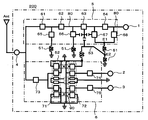
- a perspective view of a duplexer 200 according to an embodiment of the present invention is shown in FIG.
- a duplexer 200 shown in FIG. 1 mainly includes a circuit board 100 formed by laminating a plurality of dielectric layers and a piezoelectric substrate 101 mounted on the circuit board 100.
- the piezoelectric substrate 101 is mounted on the second main surface 100 ⁇ / b> B of the circuit substrate 100.
- the transmission filter 5 as the first filter and the reception filter 6 as the second filter are formed on the surface (the third main surface 101A) facing the second main surface 100B of the circuit substrate 100 of the piezoelectric substrate 101. Has been.
- the piezoelectric substrate 101 is set to a size slightly smaller than the circuit substrate 100, and is entirely covered and protected by a sealing resin 103 (indicated by a dotted line in the figure).
- the circuit board 100 has a thickness of 350 ⁇ m to 400 ⁇ m, for example, and the piezoelectric substrate 101 has a thickness of 230 ⁇ m to 280 ⁇ m, for example.
- FIG. 2 is a plan perspective view of the piezoelectric substrate 101 used in the duplexer according to the present embodiment when viewed from the fourth main surface 101B side opposite to the third main surface 101A.
- the transmission filter 5 and the reception filter 6 in the present embodiment are composed of surface acoustic wave filters.
- approximate regions corresponding to the transmission filter 5 and the reception filter 6 are indicated by alternate long and short dash lines.
- the transmission filter 5 forms a ladder filter circuit by connecting a plurality of surface acoustic wave resonators in series or in parallel as shown in FIG. Specifically, in the path from the antenna pad 4 ′ to the transmission signal pad 1 ′, the series resonators 61, 62, 63, 64 are connected in series via the resonator connection wiring 80, and the series resonator 61 , 62, 63, 64 are arranged between the resonator connection wiring 80 and the ground pads GP1, GP2, GP3, and parallel resonators 65, 66, 67, 68 are arranged.
- the reception filter 6 constitutes a longitudinal multimode filter circuit, and as shown in FIG. 2, two dual-mode surface acoustic wave elements 71 and 72 and three surface acoustic wave resonators.
- the surface acoustic wave filter includes 73, 74, and 75.
- the wiring 81 that connects the surface acoustic wave element 72 and the surface acoustic wave resonator 74 and the wiring 81 that connects the surface acoustic wave element 72 and the ground pad GP 5 include the insulator 90. Crossing three-dimensionally by sandwiching between both wires. Even in other parts, the wirings having different potentials intersect with each other through a three-dimensional insulator 90.
- a first annular wiring 83 is formed on the third main surface 101 A of the piezoelectric substrate 101 so as to surround the transmission filter 5 and the reception filter 6.
- the first annular wiring 83 is joined to the second annular wiring 19 provided on the second main surface 100B of the circuit board 100 via a joining material such as solder.
- the transmission filter 5 and the reception filter 6 are joined to the first annular wiring 83 and the second annular wiring 19, the second main surface 100B of the circuit board 100, and the third main surface 101A of the piezoelectric substrate 101. It will be hermetically sealed in the space surrounded by.
- the transmission signal pad 1 ′ is electrically connected to the transmission signal terminal 1 of the circuit board 100, and the reception signal pads 2 ′ and 3 ′ are electrically connected to the reception signal terminals 2 and 3 of the circuit board 100, respectively.
- the antenna pad 4 ′ is electrically connected to the antenna terminal 4 of the circuit board 100.
- the transmission filter 5 and the reception filter 6 may be manufactured on the same piezoelectric substrate or may be manufactured on separate piezoelectric substrates.
- the transmission filter 5 and the reception filter 6 are arranged on the same piezoelectric substrate as shown in FIG. Due to the manufacture of the duplexer, manufacturing variations may occur in each of the transmission filter 5 and the reception filter 6, but when each filter is manufactured on a separate substrate, there is a manufacturing variation in the manufacturing variations. Since the filter and the reception filter are combined, the optimum inductance value of the line pattern of the matching circuit may be different depending on the combination. On the other hand, when two filters are fabricated on the same piezoelectric substrate, the filters are fabricated at substantially the same location on the wafer. In this case, the optimum inductance value is almost the same for any substrate cut out from the wafer, and variations due to combinations can be reduced.
- the transmission filter 5 and the reception filter 6 shown in the equivalent circuit diagram of FIG. 3 are formed.
- the transmission filter 5 is disposed between the antenna terminal 4 and the transmission signal terminal 1
- the reception filter 6 is disposed between the antenna terminal 4 and the reception signal terminals 2 and 3.
- the transmission filter 5 and the reception filter 6 are set to have different passband frequencies.
- the pass frequency band of the reception filter 6 is set to be higher than the pass frequency band of the transmission filter 5.
- the pass frequency band of the reception filter 6 is 869 to 894 MHz.
- the pass frequency band of the transmission filter 5 is 824 to 849 MHz.
- the transmission filter 5 is an unbalanced signal filter for both input and output signals
- the reception filter 6 is an unbalanced signal input signal and a balanced signal output signal. That is, in FIG. 3, an unbalanced signal is input to the transmission signal terminal 1, and a balanced signal is output from the reception signal terminals 2 and 3.
- the parallel resonators 65 to 68 of the transmission filter 5 are each connected to the ground terminal via the first connection wiring 51.
- the first connection wiring 51 has an inductance of a predetermined size, and the inductance and the capacitance of the parallel resonator resonate at a predetermined frequency, thereby forming an attenuation pole outside the band, and attenuation outside the band. The amount is increased.
- the surface acoustic wave elements 71 and 72 of the reception filter 6 are connected to the ground terminal via the second connection wiring 52.
- the first connection wiring 51 and the second connection wiring 52 are connected by a third connection wiring 53.
- the third connection wiring 53 is electromagnetically coupled to at least one of the series resonators 61 to 64 and the parallel resonators 65 to 68 constituting the transmission filter 5 and the resonator connection wiring 80 that connects these resonators. ing.
- FIG. 3 shows a mode in which the third connection wiring 53 is capacitively coupled to the series resonator 63 and the parallel resonators 66 and 67.
- the electromagnetic field coupling is a coupling including at least one of capacitive coupling and inductive coupling.
- the first connection wiring 51 and the second connection wiring 52 are connected by the third connection wiring 53, and the third connection wiring 53 is connected to the series resonators 61 to 64, the parallel resonators 65 to 68, and their resonances.
- the isolation characteristics can be improved with almost no deterioration in insertion loss.
- connection portion between the first connection wiring 51 and the third connection wiring 53 is connected to the parallel resonators 67 and 68 in the first connection wiring 51. It is located in a portion closer to the other end E2 that is a connection portion with the ground terminal than the one end E1 that is a portion.
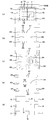
- FIG. 4 shows each dielectric layer constituting the circuit board 100.
- the circuit board 100 used in the duplexer 200 is formed by laminating two dielectric layers.
- 4A is a plan view of the first layer, assuming that the layer on the second main surface 100B side of the circuit board 100 is the first layer and the layer on the first main surface 100A side is the second layer.
- C is a plan view of the second layer, and (d) of FIG. 4 corresponds to a plan perspective view of the second layer.
- 4B is a diagram showing the positions of vias formed in the first layer connecting the first-layer wiring pattern and the second-layer wiring pattern, and FIG.
- the main surface of the first layer corresponds to the second main surface 100B of the circuit board, and the back surface of the second layer corresponds to the first main surface 100A of the circuit board.
- the region T indicated by the alternate long and short dash line generally corresponds to the region where the transmission filter 5 is disposed oppositely, and the region R illustrated by the alternate long and short dashed line is disposed opposite to the reception filter 6. Generally corresponds to the area.
- a terminal group including a transmission signal terminal 1, reception signal terminals 2, 3, an antenna terminal 4, and a plurality of ground terminals G is formed on the first main surface 100A of the circuit board. ing. These terminal groups are connected to the transmission filter 5 and the reception filter 6 through wiring patterns and vias provided in each layer of the circuit board 100.
- the transmission signal input from the transmission signal terminal 1 is input to the transmission filter 5 via the via 40, the wiring pattern 30, the via 20, and the wiring pattern 10.
- the transmission signal output from the transmission filter 5 is output from the antenna terminal 4 via the wiring pattern 11, the via 21, the wiring pattern 31, and the via 41.
- the reception signal input from the antenna terminal 4 is input to the reception filter 6 via the via 41, the wiring pattern 31, the via 21, and the wiring pattern 11.
- the reception signal input to the reception filter 6 is output from the reception signal terminals 2 and 3 through the wiring patterns 12 and 13, the vias 22 and 23, the wiring patterns 32 and 33, and the vias 42 and 43.
- the first connection wiring 51 that connects the parallel resonators 67 and 68 of the transmission filter 5 and the ground terminal G includes a first wiring pattern 15, a first via 24, a second wiring pattern 34, and It consists of a second-layer via 44.
- the wiring pattern 34 in the second layer is formed in a spiral shape, thereby giving an inductance having a predetermined size to the first connection wiring 51.
- the second connection wiring 52 that connects the reception filter 6 and the ground terminal G is from the first layer wiring pattern 18, the first layer via 25, the second layer wiring pattern 35, and the second layer via 45. Become.
- the third connection wiring 53 that connects the first connection wiring 51 and the second connection wiring 52 includes the first-layer wiring pattern 16 and the first-layer vias 26 and 27, and the via 26 is the first connection wiring 51.
- the via 27 is connected to the second-layer wiring pattern 35 constituting a part of the second connection wiring 52.
- the wiring pattern 16 that constitutes a part of the third connection wiring 53 is located on the second main surface 100B of the circuit board 100, and the series resonators 61 to 64 and the parallel resonator that constitute the transmission filter 5. 65 to 68 are opposed to at least one of the resonator connection wirings 80 for connecting these resonators. As a result, the third connection wiring 53 and the resonators and wirings constituting the transmission filter 5 can be electromagnetically coupled.
- the dielectric material constituting the circuit board 100 for example, ceramics mainly composed of alumina, glass ceramics that can be sintered at a low temperature, or glass epoxy resins mainly composed of organic materials are used.
- a green sheet was produced by forming a slurry in which a metal oxide such as ceramics and an organic binder were homogeneously kneaded with an organic solvent into a sheet, and a desired conductor pattern or via was formed. Thereafter, these green sheets are laminated and pressure-bonded to form an integrated body, and then fired.
- Each wiring pattern is made of a conductor on the surface of each dielectric layer, and the dielectric layers are connected by vias filled with the conductor.
- silver, an alloy obtained by adding palladium to silver, tungsten, copper, gold, or the like can be used as the conductor.
- These wiring patterns are formed by forming a metal conductor by screen printing or a combination of a film forming method such as vapor deposition or sputtering and etching.
- Ni or Au is further formed on the surface if necessary for good bonding with the connection terminal of the filter. You may perform plating, such as.
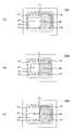
- FIGS. 5A to 5C are plan views of the first layer of the circuit board 100 used in each of the duplexers of Comparative Examples 1 and 2 and the duplexer 200 of the embodiment. The position of the first-layer via is superimposed on this wiring pattern. Note that the second-layer wiring pattern, vias, and terminal group are the same as those shown in FIG. 4 in FIGS.
- FIG. 5A shows the first layer plane of the duplexer of the first comparative example in which the third connection wiring 53 is connected to the second connection wiring 52 but is not connected to the first connection wiring 51.
- the via 26 connected to one end of the wiring pattern 16 provided in FIG. 4 is not provided.
- FIG. 5B shows the first layer plane of the duplexer of the comparative example 2 in which the third connection wiring 53 is connected to the first connection wiring 51 but is not connected to the second connection wiring 52. It is a figure and the via
- FIG. 5C is a plan view of the first layer of the duplexer 200 shown in FIG. 4, in which the first connection wiring 51 and the second connection wiring 52 are connected via the third connection wiring 53. Has been.
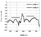
- the horizontal axis represents frequency (MHz) and the vertical axis represents isolation (dB).
- the duplexer 200 of the embodiment has improved isolation characteristics in the reception band as compared with the duplexers of Comparative Examples 1 and 2. From this result, it was confirmed that it is effective to connect the first connection wiring 51 and the second connection wiring 52 to improve the isolation characteristics of the duplexer.
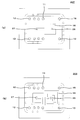
- FIG. 7 is a plan view of the first layer of the circuit board 100, and shows the via positions superimposed on the wiring pattern of the first layer.
- the shape of the wiring pattern 16 constituting the third connection wiring 53 is changed.
- the shaded area is an area corresponding to the transmission filter 5. Note that the wiring patterns, vias, and terminal groups in the second layer are the same as those shown in FIG. 4 in FIGS.
- FIG. 7A is a plan view of the first layer of the duplexer 201 when the area of the wiring pattern 16 facing the transmission filter 5 is smaller than the area of the wiring pattern 16 facing the reception filter 6. It is.
- FIG. 7B is a plan view of the first layer of the duplexer 202 when the area of the wiring pattern 16 facing the transmission filter 5 is equal to the area of the wiring pattern 16 facing the reception filter 6. is there.
- FIG. 7C is a plan view of the first layer of the duplexer 203 when the area of the wiring pattern 16 facing the transmission filter 5 is larger than the area of the wiring pattern 16 facing the reception filter 6. It is.
- the horizontal axis represents frequency (MHz) and the vertical axis represents isolation (dB).
- the duplexer 201 having a small facing area between the wiring pattern 16 and the transmitting filter 5 does not have a large attenuation pole, whereas the facing area facing the transmitting filter 5 is not formed. It can be seen that in the duplexers 202 and 203 having a large value, a relatively large attenuation pole is formed in the reception band, and the isolation characteristics are improved.
- FIG. 9 is a plan view of the first layer of the circuit board 100, and shows the positions of vias superimposed on the wiring pattern of the first layer.
- the shape of the wiring pattern 16 constituting the third connection wiring 53 is changed.
- the hatched area is an area corresponding to the transmission filter 5. Note that the wiring patterns, vias, and terminal groups in the second layer are the same as those shown in FIG. 4 in FIGS. 9A to 9C.
- FIG. 9A shows a duplexer 204 in which the area of the wiring pattern 16 facing the transmission filter 5 is relatively large.
- FIG. 9B shows the area of the wiring pattern 16 facing the transmission filter 5.
- 9C is a demultiplexer 206 in which the area of the wiring pattern 16 facing the transmission filter 5 is smaller than that of the demultiplexer 205.
- FIG. That is, the facing area of the wiring pattern 16 to the transmission filter 5 is gradually reduced in the order of the duplexer 204, the duplexer 205, and the duplexer 206.
- the horizontal axis represents frequency (MHz) and the vertical axis represents isolation characteristics (dB).
- MHz frequency
- dB isolation characteristics
- FIG. 11 is a plan view of the first layer of the circuit board 100, and shows via positions superimposed on the first-layer wiring pattern.
- the shape of the wiring pattern 16 constituting the third connection wiring 53 is changed. Note that the wiring patterns, vias, and terminal groups in the second layer are the same as those shown in FIG. 4 in both (a) and (b) of FIG.
- FIG. 11A and 11B are duplexers in which the inductance of the wiring pattern 16 is changed with the facing area of the wiring pattern 16 facing the transmission filter 5 being equal
- FIG. 11B shows a duplexer 207 in which the portion of the wiring pattern 16 facing the transmission filter 5 is a solid pattern and the inductance of the wiring pattern 16 is reduced
- FIG. 11B is a diagram of the wiring pattern 16 facing the transmission filter 5. This is a duplexer 208 in which the part to be spiraled is formed and the inductance of the wiring pattern 16 is increased.
- duplexer 207 and duplexer 208 were examined by simulation calculation. The result is shown in FIG.
- the horizontal axis represents frequency (MHz) and the vertical axis represents isolation (dB).
- the branching filter 208 has improved isolation characteristics than the branching filter 207. From this result, it was confirmed that the isolation characteristics were improved by increasing the inductance of the third connection wiring 53 that is electromagnetically coupled to the transmission filter 5.
- FIG. 13 is a graph showing insertion loss characteristics of the duplexer 200 of the embodiment having the wiring pattern 16 shown in FIG. 4 and the duplexer of Comparative Example 3 in which only the wiring pattern 16 is deleted from the duplexer of the embodiment 200. is there. 13A shows the insertion loss in the transmission band, and FIG. 13B shows the insertion loss in the reception band.
- the duplexer 200 showed almost no difference in insertion loss characteristics from the duplexer of Comparative Example 3.
- FIG. 14 is a graph showing the isolation characteristics of the duplexer 200 and the duplexer of Comparative Example 3. As can be seen from this graph, the duplexer 200 is more isolated than the duplexer of Comparative Example 3. The characteristics have improved.
- the insertion loss characteristic is obtained by connecting the first connection wiring 51 and the second connection wiring 52 by the third connection wiring 53 and electromagnetically coupling the third connection wiring 53 to the transmission filter 5. It was confirmed that the isolation characteristics of the duplexer can be improved while suppressing deterioration of the duplexer.
- FIG. 15 is a perspective view of the communication module component 400 according to the present embodiment.
- the communication module component 400 includes, in addition to the duplexer 200, a power amplifier PA, a bandpass filter BPF, and the like, and is used as a transmission module such as a mobile phone.
- the communication module component 400 is obtained by mounting the duplexer 200, the power amplifier PA, and the bandpass filter BPF on the upper surface of the module substrate 300, and coating these components with a resin 301.
- the communication module of the present embodiment is excellent in electrical characteristics by mounting the duplexer 200 described above. It is also possible to form the internal pattern of the circuit board 100 of the duplexer 200 inside the module substrate 300 and mount the piezoelectric substrate 101 directly on the module substrate 300.
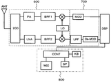
- FIG. 16 is a block diagram of a communication apparatus according to the present embodiment. 16 includes an antenna ANT, an RF circuit 600 connected to the antenna ANT, an IF circuit 700 connected to the RF circuit 600, a signal processing circuit DSP connected to the IF circuit, and a signal processing circuit. And an interface unit 800 connected to the DSP.
- the RF circuit 600 includes a duplexer 200, a power amplifier PA, a transmission bandpass filter BPF1, a low noise amplifier LNA, a reception bandpass filter BPF2, and a local oscillator LO.
- the IF circuit 700 includes a modulator MOD, a low-pass filter LPS, and a demodulator De-MOD.
- the user interface unit 800 includes a control unit CONT, an operation unit KB, a microphone MIC, and a speaker SP.
- the audio signal input from the microphone MIC is A / D converted by a DSP (Digital Signal Processor), then modulated by the modulator MOD, and further, the frequency is output by the mixer using the oscillation signal of the local oscillator LO. Converted.
- the output of the mixer passes through the transmission bandpass filter BPF1 and the power amplifier PA, passes through the duplexer 200, and is output to the antenna ANT.
- a reception signal from the antenna ANT passes through the duplexer 200, and is input to the mixer through the low noise amplifier LNA and the reception band pass filter BPF2.
- the mixer converts the frequency of the received signal using the oscillation signal of the local oscillator LO, and the converted signal passes through the low-pass filter LPF, is demodulated by the demodulator De-MOD, and further D / A converted by the DSP, and the speaker An audio signal is output from. Since the communication device illustrated in FIG. 10 includes the duplexer 200, a call with less noise is possible.
- the transmission signal terminal 1 is an example of a “first terminal”
- the reception signal terminals 2 and 3 are examples of a “second terminal”.
- the present invention is not limited to the above embodiment, and may be implemented in various modes.
- the configuration of the filter is not limited to this, and a thin film acoustic resonator may be used.
- the duplexer in which the pass frequency band of the transmission filter 5 is lower than the pass frequency band of the reception filter 6 has been described.
- the pass frequency band of the transmission filter 5 is higher than the pass frequency band of the reception filter 6.
- the present invention is also applicable to a duplexer.
- Second connection wiring 53 Third connection wiring 61-64: Series resonator 65-68: Parallel resonator 80: Resonator connection wiring
Landscapes
- Physics & Mathematics (AREA)
- Acoustics & Sound (AREA)
- Surface Acoustic Wave Elements And Circuit Networks Thereof (AREA)
- Transceivers (AREA)
Abstract
Priority Applications (3)
| Application Number | Priority Date | Filing Date | Title |
|---|---|---|---|
| CN201280000713.7A CN102763330B (zh) | 2011-01-31 | 2012-01-20 | 分波器及通信用模块部件 |
| JP2012530025A JP5449564B2 (ja) | 2011-01-31 | 2012-01-20 | 分波器および通信用モジュール部品 |
| US13/982,829 US9160304B2 (en) | 2011-01-31 | 2012-01-20 | Branching filter and communication module component |
Applications Claiming Priority (2)
| Application Number | Priority Date | Filing Date | Title |
|---|---|---|---|
| JP2011018606 | 2011-01-31 | ||
| JP2011-018606 | 2011-01-31 |
Publications (1)
| Publication Number | Publication Date |
|---|---|
| WO2012105337A1 true WO2012105337A1 (fr) | 2012-08-09 |
Family
ID=46602556
Family Applications (1)
| Application Number | Title | Priority Date | Filing Date |
|---|---|---|---|
| PCT/JP2012/051211 Ceased WO2012105337A1 (fr) | 2011-01-31 | 2012-01-20 | Filtre de branchement et composant de module de communication |
Country Status (4)
| Country | Link |
|---|---|
| US (1) | US9160304B2 (fr) |
| JP (2) | JP5449564B2 (fr) |
| CN (1) | CN102763330B (fr) |
| WO (1) | WO2012105337A1 (fr) |
Cited By (5)
| Publication number | Priority date | Publication date | Assignee | Title |
|---|---|---|---|---|
| JP2014082609A (ja) * | 2012-10-16 | 2014-05-08 | Taiyo Yuden Co Ltd | 弾性波デバイス及びその設計方法 |
| WO2015040921A1 (fr) * | 2013-09-17 | 2015-03-26 | 株式会社村田製作所 | Duplexeur |
| WO2015040922A1 (fr) * | 2013-09-17 | 2015-03-26 | 株式会社村田製作所 | Duplexeur |
| JP2018137826A (ja) * | 2013-10-31 | 2018-08-30 | 京セラ株式会社 | 弾性波素子、フィルタ素子および通信装置 |
| CN110999082A (zh) * | 2017-08-29 | 2020-04-10 | 京瓷株式会社 | 滤波器器件以及通信装置 |
Families Citing this family (14)
| Publication number | Priority date | Publication date | Assignee | Title |
|---|---|---|---|---|
| DE112015004609B4 (de) * | 2014-10-10 | 2022-06-23 | Murata Manufacturing Co., Ltd. | Abzweigungsvorrichtung |
| JP6421748B2 (ja) * | 2015-12-25 | 2018-11-14 | 株式会社村田製作所 | 弾性波装置 |
| JP6547848B2 (ja) * | 2015-12-25 | 2019-07-24 | 株式会社村田製作所 | 高周波モジュール |
| CN109478882B (zh) * | 2016-07-15 | 2022-08-23 | 株式会社村田制作所 | 多工器、高频前端电路以及通信终端 |
| US10109903B2 (en) * | 2016-10-06 | 2018-10-23 | Invensas Corporation | Flipped RF filters and components |
| WO2018088153A1 (fr) * | 2016-11-08 | 2018-05-17 | 株式会社村田製作所 | Appareil de filtre à ondes élastiques et multiplexeur |
| WO2018100840A1 (fr) * | 2016-11-29 | 2018-06-07 | 株式会社村田製作所 | Dispositif à ondes élastiques et son procédé de fabrication, circuit frontal haute fréquence et dispositif de communication |
| JP6669132B2 (ja) * | 2017-06-23 | 2020-03-18 | 株式会社村田製作所 | マルチプレクサ、送信装置および受信装置 |
| JP6922845B2 (ja) * | 2018-05-23 | 2021-08-18 | 株式会社村田製作所 | マルチプレクサおよび通信装置 |
| KR102546477B1 (ko) * | 2018-06-21 | 2023-06-22 | 가부시키가이샤 무라타 세이사쿠쇼 | 필터 및 멀티플렉서 |
| US11108379B2 (en) * | 2018-09-05 | 2021-08-31 | Resonant Inc. | High isolation surface acoustic wave duplexer |
| JP2021097322A (ja) * | 2019-12-17 | 2021-06-24 | 株式会社村田製作所 | 高周波モジュールおよび通信装置 |
| JP2021150849A (ja) * | 2020-03-19 | 2021-09-27 | 株式会社村田製作所 | 高周波モジュール及び通信装置 |
| CN116418312A (zh) * | 2023-02-23 | 2023-07-11 | 无锡市好达电子股份有限公司 | 声表面波双工器及多工器 |
Citations (3)
| Publication number | Priority date | Publication date | Assignee | Title |
|---|---|---|---|---|
| JP2007258832A (ja) * | 2006-03-20 | 2007-10-04 | Kyocera Corp | 弾性表面波素子、弾性表面波装置、弾性表面波装置の製造方法、通信装置、送信装置および受信装置 |
| JP2009290606A (ja) * | 2008-05-29 | 2009-12-10 | Kyocera Corp | 分波器および無線通信機器 |
| JP2010021718A (ja) * | 2008-07-09 | 2010-01-28 | Nippon Dempa Kogyo Co Ltd | デュプレクサ |
Family Cites Families (10)
| Publication number | Priority date | Publication date | Assignee | Title |
|---|---|---|---|---|
| JP2800905B2 (ja) | 1991-10-28 | 1998-09-21 | 富士通株式会社 | 弾性表面波フィルタ |
| JP3900013B2 (ja) * | 2001-07-30 | 2007-04-04 | 株式会社村田製作所 | 弾性表面波分波器、通信装置 |
| JP3833569B2 (ja) * | 2001-12-21 | 2006-10-11 | 富士通メディアデバイス株式会社 | 分波器及びこれを用いた電子装置 |
| JP2005124139A (ja) * | 2003-09-25 | 2005-05-12 | Murata Mfg Co Ltd | 分波器、通信機 |
| US7298231B2 (en) * | 2004-05-27 | 2007-11-20 | Kyocera Corporation | Surface acoustic wave device and communication apparatus |
| US9035721B2 (en) | 2008-07-30 | 2015-05-19 | Kyocera Corporation | Duplexer, communication module component, and communication device |
| JP2010068079A (ja) * | 2008-09-09 | 2010-03-25 | Panasonic Corp | アンテナ共用器、高周波回路及び無線通信装置 |
| JP4816710B2 (ja) * | 2008-10-30 | 2011-11-16 | 株式会社村田製作所 | 分波器 |
| JP5056952B2 (ja) * | 2008-11-04 | 2012-10-24 | 株式会社村田製作所 | 弾性波フィルタ装置および、それを備えるモジュール |
| US8902020B2 (en) * | 2009-07-27 | 2014-12-02 | Avago Technologies General Ip (Singapore) Pte. Ltd. | Resonator filter with multiple cross-couplings |
-
2012
- 2012-01-20 WO PCT/JP2012/051211 patent/WO2012105337A1/fr not_active Ceased
- 2012-01-20 JP JP2012530025A patent/JP5449564B2/ja active Active
- 2012-01-20 CN CN201280000713.7A patent/CN102763330B/zh active Active
- 2012-01-20 US US13/982,829 patent/US9160304B2/en active Active
-
2013
- 2013-12-25 JP JP2013267246A patent/JP5777694B2/ja not_active Expired - Fee Related
Patent Citations (3)
| Publication number | Priority date | Publication date | Assignee | Title |
|---|---|---|---|---|
| JP2007258832A (ja) * | 2006-03-20 | 2007-10-04 | Kyocera Corp | 弾性表面波素子、弾性表面波装置、弾性表面波装置の製造方法、通信装置、送信装置および受信装置 |
| JP2009290606A (ja) * | 2008-05-29 | 2009-12-10 | Kyocera Corp | 分波器および無線通信機器 |
| JP2010021718A (ja) * | 2008-07-09 | 2010-01-28 | Nippon Dempa Kogyo Co Ltd | デュプレクサ |
Cited By (10)
| Publication number | Priority date | Publication date | Assignee | Title |
|---|---|---|---|---|
| JP2014082609A (ja) * | 2012-10-16 | 2014-05-08 | Taiyo Yuden Co Ltd | 弾性波デバイス及びその設計方法 |
| WO2015040921A1 (fr) * | 2013-09-17 | 2015-03-26 | 株式会社村田製作所 | Duplexeur |
| WO2015040922A1 (fr) * | 2013-09-17 | 2015-03-26 | 株式会社村田製作所 | Duplexeur |
| CN105531927A (zh) * | 2013-09-17 | 2016-04-27 | 株式会社村田制作所 | 双工器 |
| US9762209B2 (en) | 2013-09-17 | 2017-09-12 | Murata Manufacturing Co., Ltd. | Duplexer with a series trap element and a specifically connected capacitance or elastic wave resonator |
| US9806693B2 (en) | 2013-09-17 | 2017-10-31 | Murata Manufacturing Co., Ltd. | Duplexer with a ladder filter portion and a specifically connected capacitor or elastic wave resonator |
| CN105531927B (zh) * | 2013-09-17 | 2018-03-30 | 株式会社村田制作所 | 双工器 |
| JP2018137826A (ja) * | 2013-10-31 | 2018-08-30 | 京セラ株式会社 | 弾性波素子、フィルタ素子および通信装置 |
| CN110999082A (zh) * | 2017-08-29 | 2020-04-10 | 京瓷株式会社 | 滤波器器件以及通信装置 |
| CN110999082B (zh) * | 2017-08-29 | 2023-07-21 | 京瓷株式会社 | 滤波器器件以及通信装置 |
Also Published As
| Publication number | Publication date |
|---|---|
| JP2014060806A (ja) | 2014-04-03 |
| CN102763330A (zh) | 2012-10-31 |
| JP5777694B2 (ja) | 2015-09-09 |
| US20130307639A1 (en) | 2013-11-21 |
| JPWO2012105337A1 (ja) | 2014-07-03 |
| JP5449564B2 (ja) | 2014-03-19 |
| US9160304B2 (en) | 2015-10-13 |
| CN102763330B (zh) | 2015-02-25 |
Similar Documents
| Publication | Publication Date | Title |
|---|---|---|
| JP5449564B2 (ja) | 分波器および通信用モジュール部品 | |
| JP5334924B2 (ja) | 分波器、通信用モジュール部品、及び通信装置 | |
| JP6468290B2 (ja) | 高周波モジュール | |
| JP5230270B2 (ja) | 分波器および無線通信機器 | |
| US7619491B2 (en) | Elastic wave duplexer | |
| CN101395797B (zh) | 信号分离器及通信装置 | |
| US7053731B2 (en) | Duplexer using surface acoustic wave filters | |
| US7924118B2 (en) | Duplexer and elastic wave device | |
| JP4926179B2 (ja) | 分波器デバイス用回路基板、分波器、及び通信装置 | |
| JP5583977B2 (ja) | フィルタ、分波器、通信モジュール、および通信装置 | |
| WO2019065027A1 (fr) | Dispositif de filtre hybride et multiplexeur | |
| JP5043128B2 (ja) | フィルタおよび通信装置 | |
| KR100697767B1 (ko) | 분파기 및 전자 장치 | |
| US11558035B2 (en) | Multiplexer | |
| CN100511989C (zh) | 滤波装置以及使用它的多波段滤波器、分频器及通信装置 | |
| JP2003152590A (ja) | アンテナスイッチモジュール | |
| JP5937477B2 (ja) | 分波器および通信用モジュール部品 | |
| CN102571030A (zh) | 双工器 |
Legal Events
| Date | Code | Title | Description |
|---|---|---|---|
| WWE | Wipo information: entry into national phase |
Ref document number: 201280000713.7 Country of ref document: CN |
|
| WWE | Wipo information: entry into national phase |
Ref document number: 2012530025 Country of ref document: JP |
|
| 121 | Ep: the epo has been informed by wipo that ep was designated in this application |
Ref document number: 12741848 Country of ref document: EP Kind code of ref document: A1 |
|
| NENP | Non-entry into the national phase |
Ref country code: DE |
|
| WWE | Wipo information: entry into national phase |
Ref document number: 13982829 Country of ref document: US |
|
| 122 | Ep: pct application non-entry in european phase |
Ref document number: 12741848 Country of ref document: EP Kind code of ref document: A1 |