WO2012108139A1 - Commutateur sélectif en longueur d'onde - Google Patents
Commutateur sélectif en longueur d'onde Download PDFInfo
- Publication number
- WO2012108139A1 WO2012108139A1 PCT/JP2012/000575 JP2012000575W WO2012108139A1 WO 2012108139 A1 WO2012108139 A1 WO 2012108139A1 JP 2012000575 W JP2012000575 W JP 2012000575W WO 2012108139 A1 WO2012108139 A1 WO 2012108139A1
- Authority
- WO
- WIPO (PCT)
- Prior art keywords
- input
- light
- wavelength
- condensing
- condensing position
- Prior art date
- Legal status (The legal status is an assumption and is not a legal conclusion. Google has not performed a legal analysis and makes no representation as to the accuracy of the status listed.)
- Ceased
Links
Images






















Classifications
-
- G—PHYSICS
- G02—OPTICS
- G02B—OPTICAL ELEMENTS, SYSTEMS OR APPARATUS
- G02B6/00—Light guides; Structural details of arrangements comprising light guides and other optical elements, e.g. couplings
- G02B6/24—Coupling light guides
- G02B6/26—Optical coupling means
- G02B6/35—Optical coupling means having switching means
- G02B6/354—Switching arrangements, i.e. number of input/output ports and interconnection types
- G02B6/356—Switching arrangements, i.e. number of input/output ports and interconnection types in an optical cross-connect device, e.g. routing and switching aspects of interconnecting different paths propagating different wavelengths to (re)configure the various input and output links
-
- G—PHYSICS
- G02—OPTICS
- G02B—OPTICAL ELEMENTS, SYSTEMS OR APPARATUS
- G02B6/00—Light guides; Structural details of arrangements comprising light guides and other optical elements, e.g. couplings
- G02B6/24—Coupling light guides
- G02B6/26—Optical coupling means
- G02B6/35—Optical coupling means having switching means
- G02B6/351—Optical coupling means having switching means involving stationary waveguides with moving interposed optical elements
- G02B6/3512—Optical coupling means having switching means involving stationary waveguides with moving interposed optical elements the optical element being reflective, e.g. mirror
-
- G—PHYSICS
- G02—OPTICS
- G02B—OPTICAL ELEMENTS, SYSTEMS OR APPARATUS
- G02B6/00—Light guides; Structural details of arrangements comprising light guides and other optical elements, e.g. couplings
- G02B6/24—Coupling light guides
- G02B6/26—Optical coupling means
- G02B6/35—Optical coupling means having switching means
- G02B6/354—Switching arrangements, i.e. number of input/output ports and interconnection types
- G02B6/3554—3D constellations, i.e. with switching elements and switched beams located in a volume
- G02B6/3556—NxM switch, i.e. regular arrays of switches elements of matrix type constellation
Definitions
- the present invention relates to a wavelength selective switch capable of branching or combining light of different wavelengths.
- a wavelength selective switch used for optical wavelength division multiplexing communication for example, as described in Patent Document 1 and Patent Document 2, at least one input port, at least one output port, a dispersion element, and a light collecting element And a deflector are used.
- wavelength multiplexed light input from one optical fiber of an optical fiber array (input port and output port) into the wavelength selective switch is converted into a parallel beam by a microlens array.
- a diffraction grating collimated to each wavelength by a diffraction grating (dispersion element), and are collected by a condensing lens on a different mirror element (deflection element) of the MEMS mirror array (deflection unit) for each wavelength, in a different direction for each wavelength. Deflected and output.
- the wavelength multiplexed light input from the input port and the output port arranged in an array is converged by using a lens and a cylindrical lens at the front stage of the diffraction grating. Then, the light expanded after passing through the focal position is converted into a parallel light beam by a convex lens and is incident on a diffraction grating (dispersing element).
- the cylindrical lens has refracting power in a direction orthogonal to the arrangement direction of the input / output ports, and forms an elliptical spot on the mirror element of the MEMS mirror array which is a deflection unit.
- the wavelength selective switch not only disperses wavelength-multiplexed light for each wavelength and outputs it from different output ports, but also controls the mirror elements to multiplex and output the light to the same output port It can also be made.
- Each wavelength selective switch receives light from an input port at a different position of the wavelength selective switch and outputs it from an output port at a different position.
- end faces where light enters and exits are arranged in series to input or output light into the wavelength selective switch.
- the height position of the light passing through the input and output ports is different for each input port and each output port. Therefore, curvature of field due to the distance from the optical axis for each port occurs in the vicinity of the deflecting element surface of the deflecting element, which is the condensing position.
- the position of the light collection position is shifted depending on the position of the input / output ports in the arrangement direction. Obviously, the position shift of the condensing position becomes more significant as the number of input / output ports increases.
- the condensing position shifts in the vicinity of the deflection element, the spot of light on the deflection element surface such as the mirror of the deflection element becomes large. Thereby, the coupling efficiency of the output light to the input / output port is lowered, and the communication quality is deteriorated.
- the deflection elements are arranged in series in the dispersion direction of the dispersion element, the spread of the beam in the dispersion direction greatly reduces the communication quality.
- an object of the present invention which has been made paying attention to these points, is to provide a wavelength selective switch that improves the communication quality by correcting the condensing position shift in the deflecting unit.
- the invention of the wavelength selective switch according to the first aspect of achieving the above object is as follows: At least one input port; A dispersion unit for dispersing wavelength-multiplexed input light input from the input port into light for each wavelength; A condensing element that condenses light for each wavelength dispersed by the dispersion unit; A deflecting unit having a deflecting element for deflecting light of each wavelength collected by the condensing element; At least one output port that outputs light for each wavelength deflected by the deflecting unit as output light; A condensing position deviation correction element that is arranged in the optical path between the input port and the dispersion unit or in the dispersion part, and corrects the deviation of the light collection position of the light for each wavelength with respect to the deflection element based on the arrangement of the input port; , It is characterized by providing.
- correctioning the deviation of the condensing position means correcting the condensing position so as to be conjugate with the output end face of the output port, and the condensing position is not necessarily changed by the deflection element surface (mirror). Do not match on the surface).
- the condensing position deviation correcting element is used to correct the deviation of the condensing position of the light for each wavelength with respect to the polarization plane of the deflecting element, which occurs based on the arrangement of the input port, It is possible to improve the communication quality by correcting the condensing position deviation in the unit.
- FIG. 4A It is a figure explaining the shape of the refractive surface of the condensing position shift correction element of FIG. 4A. It is a perspective view which shows the other example of the condensing position shift correction element of FIG. It is a figure explaining the shape of the refractive surface of the condensing position shift correction element of FIG. 5A. It is a perspective view which shows the other example of the condensing position shift correction element of FIG. It is a figure explaining the shape of the refractive surface of the condensing position shift correction element of FIG. 6A. It is a top view which shows a part of structure of the wavelength selective switch which concerns on 2nd Embodiment of this invention. It is a perspective view which shows an example of the condensing position shift correction element of FIG.
- FIG. 10 is a perspective view which shows the other example of the condensing position shift correction element of FIG. It is a perspective view explaining the structure of the wavelength selective switch which concerns on 3rd Embodiment of this invention, and the beam which passes this. It is a perspective view which shows an example of the condensing position shift correction element of FIG. It is a figure explaining the shape of the refractive surface of the condensing position shift correction element of FIG. 10A. 10 is a graph showing a design example of the condensing position deviation correction element in FIG. 9. It is a graph which shows the simulation result of the shift
- FIG. 22B is a diagram showing a lattice of the dispersion element in FIGS. 21A and 21B. It is a perspective view which shows a part of dispersion element of FIG. 21A and FIG. 21B with a cross section. It is a perspective view which shows the light beam from the input / output port of FIG. 21A and FIG. 21B to the primary condensing surface vicinity. It is a side view explaining the optical path from the primary condensing surface Sf vicinity to the deflector 17.
- FIG. 22B is a diagram showing a lattice of the dispersion element in FIGS. 21A and 21B. It is a perspective view which shows a part of dispersion element of FIG. 21A and FIG. 21B with a cross section. It is a perspective view which shows the light beam from the input / output port of FIG. 21A and FIG. 21B to the primary condensing surface vicinity. It is a side view explaining the optical path from the primary condensing surface Sf vicinity to the
- FIG. It is a top view explaining the optical path from the primary condensing surface Sf vicinity to the deflector 17.
- FIG. It is a top view which shows the structure and optical path from the primary condensing surface vicinity of the wavelength selective switch which concerns on 10th Embodiment of this invention to a deflector. It is a graph which shows the pitch of the dispersion element of FIG. It is a graph which shows distance (DELTA) z 'of the mirror surface Sm and the condensing position Sm' of the light ray from each port.
- DELTA distance
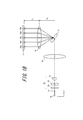
- (First embodiment) 1A and 1B are a side view and a top view, respectively, showing the configuration of the wavelength selective switch according to the first embodiment of the present invention.
- the wavelength selective switch 1 includes an input / output unit 10, a microlens array 11, a condensing position deviation correction element 20, cylindrical lenses 12 and 13, a lens 14, a dispersive element (diffraction grating) 15 constituting a dispersive part, and a condensing element.
- deviation part are comprised.
- the cylindrical lens 12 is a first optical member
- the cylindrical lens 13 is a second optical member.
- the input / output unit 10 includes input ports 10a to 10c and 10e and an output port 10d configured by optical fibers arranged in an array.
- the input ports 10a to 10c and 10e and the output port 10d are used to input wavelength-multiplexed signal light from the outside of the wavelength selective switch 1 and to output signal light to the outside.
- the input ports 10a to 10c and 10e and the output port 10d will be collectively referred to as input / output ports 10a to 10e as appropriate.
- One end of each optical fiber is in the wavelength selective switch 1, and the other end is connected to the outside of the wavelength selective switch 1.
- the number of input / output ports is, for example, 10 or more, and a larger number of input / output ports can be provided. However, in FIG. 1A, for convenience of explanation, five input / output ports 10a to 10e centering on the input / output port 10c are provided. Only shown.
- the input / output ports 10a to 10e and the microlenses in the microlens array 11 are paired.
- Each microlens converts the light input from the input / output ports 10a to 10c and 10e into a parallel light beam, and couples the parallel light beam output to the input / output port 10d to an optical fiber. Further, the light input into the wavelength selective switch 1 through the input / output ports 10a to 10c and 10e and the microlens of each microlens array 11, and the light output from the wavelength selective switch 1 through the input / output port 10d. The light beams become parallel light beams.
- the traveling direction of the parallel light flux that has passed through the input / output ports 10a to 10e and the microlens array 11 is defined as an optical axis direction (z direction: horizontal direction in FIG. 1A).
- This optical axis direction is also the optical axis direction of the optical system composed of the synthetic lens formed by the cylindrical lenses 12 and 13 and the lens 14.
- the direction in which the input / output ports 10a to 10e and the microlens array 11 are arranged is defined as a first direction (y direction: vertical direction in FIG. 1A).
- the optical axis direction and the first direction are orthogonal to each other.
- a direction orthogonal to each of the optical axis direction and the first direction (y direction) is referred to as a second direction (x direction).
- a deflecting member such as a mirror or a prism (not shown) is arranged to bend the optical path in the optical path of the actual wavelength selective switch
- the description of the x direction and the y direction is such a deflecting member. It is assumed that it is used on the premise of a virtual optical system that does not have any.
- the condensing position deviation correction element 20 is a transmissive element having a refractive power only in the second direction (x direction).
- the refractive power in the second direction (x direction) changes depending on the position in the first direction (y direction).
- the cylindrical lens 12 is a lens that contracts a light beam in a first direction (y direction), that is, has a refractive power in the first direction (y direction).
- the focal length in the first direction by the cylindrical lens 12 (y-direction) is f 1.
- the cylindrical lens (anamorphic lens) 13 is a lens that contracts the light beam in the second direction (x direction), that is, has a refractive power only in the second direction (x direction).
- the term “refractive power” means so-called optical power, and the degree of deflection in the direction of converging parallel light beams is positive refracting power, and the degree of deflection in the direction of diffusion is negative refracting power.
- the present application uses the term “refractive power” not only for transmissive optical elements but also for reflective elements and elements with diffraction.
- the focal length and the lens arrangement in the second direction (x direction) by the cylindrical lens 13 are the same in the first direction (x direction) in which the condensing position in the second direction (x direction) is condensed by the cylindrical lens 12. It is set to coincide with the condensing position. That is, the focal length of the cylindrical lens 13 is shorter than the focal length f 1 of the cylindrical lens 12.
- the input light converted into a parallel light beam by the microlens array 11 is condensed on the primary condensing surface Sf by the condensing position deviation correction element 20, the cylindrical lens 12 and the cylindrical lens 13.
- the condensing position deviation correction element 20, the cylindrical lens 12, and the cylindrical lens 13 constitute a beam shaping optical system 25.
- the front focal position of the lens 14 coincides with the focal position of the input light by the condensing position deviation correction element 20, the cylindrical lens 12, and the cylindrical lens 13.
- the front focal position of the lens 14 is located on the primary condensing surface Sf.
- the optical axis of the optical system including the cylindrical lenses 12 and 13 and the lens 14 is arranged so as to pass through the input / output port 10c along the z-axis direction, for example.
- the dispersive element 15, the distance between the primary light-condensing surface Sf and the lens 14, the distance between the dispersion (diffractive) surface of the lens 14 and the dispersive element 15, the focal length f 3 are both equally lens 14 position Placed in.
- the dispersion element 15 is, for example, a diffraction grating in which a grating parallel to the first direction (y direction) is formed on the dispersion surface.
- a grating parallel to the first direction (y direction) is formed on the dispersion surface.
- the dispersive element one having a high light decomposition performance for each wavelength and a larger dispersion angle is desirable.
- the input light that has passed through the lens 14 enters the dispersive element 15 as a substantially parallel light flux, and is diffracted on the dispersive surface of the dispersive element 15 at different angles for each wavelength in the x direction. That is, the dispersive element 15 separates the input light into light for each wavelength included in the input light.
- the z-direction optical path from the input / output unit 10 to the deflector 17 is shown linearly in FIG. 1A.
- the lens 16 and the deflector 17 have a distance from the dispersion surface of the dispersion element 15 to the lens 16 and a distance from the lens 16 to the deflection element surface (mirror surface) of the deflection element 18 of the deflector 17, respectively. They are disposed such that the focal length f 4 of the.
- the light for each wavelength dispersed by the dispersion element 15 becomes a converged light beam parallel to each other by the lens 16 and is incident substantially perpendicularly on the deflection elements 18a to 18e corresponding to each wavelength. To do. Also, as shown in FIG.
- the input light that has passed through the condensing point on the primary condensing surface Sf is dispersed by the dispersive element 15 and then deflected by the optical axis of the lens 16 and the deflecting element 18 in the yz plane.
- Light is condensed at a height position (position in the y direction) where the element surface intersects. This means that the input light input from any of the input / output ports 10a to 10c and 10e is condensed on the deflecting element 18 (any one of 18a to 18e depending on the wavelength) at the same height position. To do.
- the deflector 17 is, for example, a MEMS mirror array, and the deflecting element 18 is a micromirror that constitutes the MEMS mirror array.
- the deflection element 18 is arranged in parallel at the height position of the optical axis of the lens 16 described above corresponding to the wavelength to be separated.
- the deflection element 18 can change the tilt by independently controlling each mirror. In particular, by changing the inclination in the yz plane in FIG. 1A, the incident light for each wavelength is reflected in a height direction different from the incident direction. As shown in FIG. 1B, when viewed from the y-axis direction, the light for each wavelength enters the deflection elements 18a to 18e perpendicularly and is reflected vertically.
- the tilt control direction of the micromirror is not limited to the yz plane.
- the tilt can be given to a rotation axis orthogonal to the rotation axis when tilting to the yz plane.
- the tilt can be given to a rotation axis orthogonal to the rotation axis when tilting to the yz plane.
- the light for each wavelength reflected by the deflecting elements 18a to 18e passes through the lens 16, is diffracted by the dispersive element 15, and passes through the optical path in the opposite direction to the input light, and is used for input in the input / output unit 10. It is output to the input / output port 10d other than the input / output port.
- the output port 10a is a distance position from the optical axis of the optical system by the cylindrical lenses 12, 13 and the lens 14 is Y 1.
- the input light from the input / output port 10a is condensed on the primary condensing surface Sf by the beam shaping optical system 25, and then the distance from the optical axis by the lens 14 is Y 2.
- the dispersion element 15 for each wavelength passes through the lens 16, and is condensed on the deflection elements 18a to 18e for each wavelength.
- the deflection direction of the corresponding deflection element 18 is controlled, and a broken line in FIG. As shown, light of a specific wavelength is reflected in a predetermined direction.
- the light having a specific wavelength reflected by the deflecting element 18 passes through the lens 16 and is output from the input / output port 10d through the dispersive element 15, the lens 14, the beam shaping optical system 25, and the corresponding microlens of the microlens array 11.
- the light beams having the plurality of wavelengths are multiplexed by the dispersion element 15.
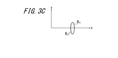
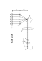
- FIG. 2 is a perspective view showing the beams from the input / output ports 10a to 10e of FIG. 3A, 3B, and 3C are diagrams showing beam shapes on the primary condensing surface Sf, a dummy plane Sd, which will be described later, and the deflection element surface Sm, respectively.
- both the input / output port 10a and the input / output port 10c are used as input ports.
- the cylindrical lens 12 whose refractive power is in the first direction (y direction) and the cylindrical lens 13 whose refractive power is in the second direction (x direction) are made to have different positions on the optical path. And a large refractive power is given by the cylindrical lens 13. That is, this optical system has a larger numerical aperture in the second direction (x direction). Therefore, on the primary light-condensing surface Sf is input light from the input-output port 10c becomes an elliptical shape B 1 as shown by the solid line in Figure 3A. Spot of elliptical shape, as shown by the solid line in FIG.
- the beam spot shape is shaped into an elliptical shape having a minor axis in the dispersion direction of the dispersive element 15, thereby increasing the resolution of the wavelength and different wavelengths. It is possible to prevent the occurrence of crosstalk due to light entering the same deflection element 18.
- the condensing position deviation correction element 20 is an element provided to correct a field curvature that occurs when the beam shaping optical system 25 is configured by the cylindrical lenses 12 and 13.
- the condensing position deviation correction element 20 is not provided, the input light emitted from the input / output port 10a having a large distance from the optical axis of the optical system including the cylindrical lenses 12, 13 and the lens 14 is larger than the deflection element surface Sm. Condensed in front. In particular, the spread of the spot in the x direction on the deflection element surface Sm in FIG. 2 degrades the communication quality of the wavelength selective switch 1.
- the converging position deviation correction element 20 is provided, and the input light emitted from the input / output port 10a is the spot B 2 having the narrowest width in the x direction on the deflection element surface Sm as indicated by a broken line in FIG. 3C. Is corrected to form.
- the lens 14 is minimized on the lens 14 side.
- a plane perpendicular to the optical axis including the position where the lateral width of the input light from the input / output port 10a is minimized is shown in FIG. 2B as a dummy plane Sd.
- the condensing position deviation correction element 20 adjusts the deviation amount ⁇ Z between the primary condensing surface Sf and the dummy plane Sd so that the condensing position deviation amount ⁇ Z ′ on the deflection element surface Sm becomes zero.
- the spots are each schematically described, and the size is not limited.
- the positional relationship between the primary condensing surface Sf and the dummy flat surface Sd is also a design example, and the dummy flat surface Sd does not necessarily need to be closer to the lens 14 than the primary condensing surface.
- FIG. 4A is a perspective view showing an example of the condensing position deviation correction element 20 of FIG.
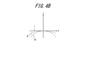
- FIG. 4B is a diagram for explaining the shape of the refracting surface of the condensing position error correction element 20a in FIG. 4A.
- the condensing position deviation correction element 20a is made of a light transmissive member such as glass.
- the front side is a curved surface having refractive power
- the back side is a flat surface.
- Each of i, ii, and iii indicates the cross-sectional shape of the refracting surface of the condensing position deviation correction element 20a by a plane parallel to the xz plane having a different y-direction position. As shown in FIGS.
- the condensing position deviation correction element 20a has substantially no refractive power in the first direction (y direction). Further, in the condensing position deviation correction element 20a, the refractive power in the second direction (x direction) differs depending on the position in the first direction (y direction). More specifically, the refractive power in the second direction (x direction) is 0 at the center position in the first direction (y direction), and the distance from the center position in the first direction (y direction) increases. , Has a larger negative refractive power in the second direction (x direction). Thereby, the condensing position of the light beam passing through the position away from the optical axis in the first direction (y direction) is shifted in the direction of the lens 14. The center position in the first direction (y direction) is a position through which the synthetic lens of the cylindrical lenses 12 and 13 and the optical axis of the lens 14 pass.
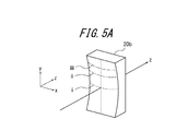
- FIG. 5A is a perspective view showing another example of the condensing position deviation correction element 20 of FIG.
- FIG. 5B is a diagram illustrating the shape of the refracting surface of the condensing position error correction element 20b of FIG. 5A.
- the condensing position deviation correction element 20b has a positive refractive power in the second direction (x direction) at the center position in the first direction (y direction), and the first direction (y As the distance increases, the refractive power in the second direction (x direction) decreases.
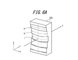
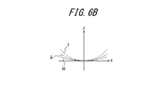
- FIG. 6A is a perspective view showing still another example of the condensing position deviation correction element 20 of FIG.
- FIG. 6B is a diagram illustrating the shape of the refracting surface of the condensing position error correction element 20c in FIG. 6A.
- the condensing position deviation correction element 20c can be used in place of the condensing position deviation correction element 20b shown in FIGS. 5A and 5B.
- the converging surface of the condensing position deviation correction element 20b in FIGS. 5A and 5B is configured by a curved surface whose curvature changes smoothly, whereas the converging surface of the condensing position deviation correction element 20c is different from each input surface.
- cylindrical surfaces having different curvatures in the second direction (x direction) are combined.
- each cylindrical surface is arranged so that the refracting surface forms a straight line in the yz plane including the z axis.
- a step is provided at the boundary of the cylindrical refracting surface corresponding to each of the different input / output ports 10a to 10e. If such a condensing position deviation correction element 20c is used, uniform refractive power in the second direction (x direction) with respect to the input light flux of each input light from the input / output ports 10a to 10c and 10e. Can affect.
- the refracting surface may not be a straight line in the yz plane including the z axis.
- the cylindrical refracting surfaces corresponding to the different input / output ports 10a to 10e may be formed by stacking concentric cylinders. Also in this case, uniform refractive power can be exerted in the second direction (x direction) on the input light fluxes of the respective input lights from the input / output ports 10a to 10c and 10e.
- the input light input from the input / output ports 10a to 10c and 10e is deflected regardless of which input / output port 10a to 10c and 10e is input. Since the condensing position shift correction element 20 for condensing by forming the narrowest elliptical spot on the deflecting element surface of the element 18 is provided, light for each wavelength dispersed by the dispersive element 15 is converted into input light. The light can be condensed with high accuracy on the deflection element surface of the deflection element 18 without depending on the positions of the input / output ports 10a to 10c and 10e.
- the correction element 20 is configured so that the input light input from the input / output port 10d is condensed with high accuracy on the deflection element surface of the deflection element 18. It is desirable.
- the condensing position deviation correcting element 20 is provided in the beam shaping optical system 25 that once condenses the input light input from the input / output ports 10a to 10c and 10e on the primary condensing surface Sf, and thus is small in size. can do.
- FIG. 7 is a top view showing a part of the configuration of the wavelength selective switch 1 according to the second embodiment of the present invention.
- the beam shaping optical system 25 of the first embodiment is replaced with the beam shaping optical system 25 ′ of FIG. 7, and the wavelength selective switch of the first embodiment is provided at the subsequent stage of the cylindrical lens 13.
- a deflector 17 including a lens 14, a dispersion element 15, a lens 16, and a deflection element 18 is disposed.
- the beam shaping optical system 25 ′ of this optical system includes a reflective condensing position shift correction element 20 ′ having a refractive power only in the second direction (x direction), a spherical mirror 12 ′, and a second direction (x And a cylindrical lens 13 having refractive power only in the direction).
- the spherical mirror 12 ′ is a first optical member
- the cylindrical lens 13 is a second optical member.
- FIG. 8A is a perspective view showing an example of the condensing position deviation correction element 20 ′ in FIG. 7.
- the front surface is a reflecting surface.
- the condensing position deviation correction element 20'a has substantially no refractive power in the first direction (y direction). Further, the condensing position deviation correction element 20'a has different refractive power in the second direction (x direction) depending on the position in the first direction (y direction). More specifically, the refractive power in the second direction (x direction) is 0 at the center position in the first direction (y direction), and the distance from the center position in the first direction (y direction) increases. , Has a larger negative refractive power in the second direction (x direction). Thereby, the condensing position of the input light passing through the position away from the optical axis in the first direction (y direction) is shifted in the direction of the lens 14.
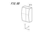
- FIG. 8B is a perspective view showing still another example of the condensing position deviation correction element 20 ′ in FIG. 7.
- This condensing position deviation correction element 20'b has substantially no refractive power in the first direction (y direction).
- the condensing position deviation correction element 20′b has a positive refractive power in the second direction (x direction) at the center position in the first direction (y direction). As the distance in the direction (y direction) increases, the refractive power in the second direction (x direction) decreases.
- the input light passing through the optical axis input from the input / output port 10c exerts a refractive power in the second direction (x direction).
- the focal length and / or the position of the cylindrical lens 13 are adjusted so that the condensing position in the second direction (x direction) is on the primary condensing surface Sf.
- Other configurations and operations are the same as those in the first embodiment.
- a reflective element can be used as the condensing position deviation correcting element 20 ′. Therefore, a transmission or reflection type condensing position deviation correction element can be appropriately selected and used according to the spatial arrangement needs of the optical system of the wavelength selective switch 1 and the frequency characteristics of the light used.
- the spherical mirror 12 ′ may be a cylindrical mirror having a refractive power only in the first direction (y direction). Further, even when the output port 10d is used as an input port, the condensing position deviation correction element so that the input light input from the input / output port 10d is condensed on the deflecting element surface of the deflecting element 18 with high accuracy. 20 is preferably configured.
- FIG. 9 is a perspective view for explaining the configuration of the wavelength selective switch 1 according to the third embodiment of the present invention and the beam passing therethrough.
- the condensing position deviation correction element 20 and the cylindrical lens 13 in the wavelength selective switch 1 of the first embodiment are replaced with one condensing position deviation correction element 21. That is, the condensing position deviation correction element 21 condenses light in the second direction (x direction) and condenses in the second direction (x direction) according to the position in the first direction (y direction). It has the effect
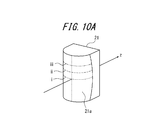
- FIG. 10A is a perspective view showing an example of the condensing position deviation correction element 21 of FIG.
- FIG. 10B is a diagram illustrating the shape of the refracting surface of the condensing position deviation correction element 21 of FIG. 10A.
- the curved surface 21a on the near side in FIG. 10A is a curved surface having refractive power, and the back side thereof is a flat surface.
- Each of i, ii, and iii indicates the cross-sectional shape of the refracting surface of the condensing position deviation correction element 21 by planes parallel to the xz planes having different positions in the y direction. As shown in FIGS.
- the refracting surface of the condensing position deviation correcting element 21 has a shape obtained by correcting the cylindrical surface. That is, the refracting surface of the condensing position deviation correction element 21 has substantially no refractive power in the first direction (y direction). Further, at the center position in the first direction (y direction), the refractive power in the second direction (x direction) has a curvature for condensing the input light in the optical axis direction on the primary condensing surface Sf. The refracting power in the second direction (x direction) decreases with increasing distance from the position in the first direction (y direction).
- the condensing position of the light beam passing through the position away from the optical axis in the second direction (x direction) is shifted in the direction of the lens 14 from the primary condensing surface Sf.
- the primary condensing surface Sf, the dummy plane Sd, and the deflection element surface Sm are respectively the same as those shown in FIGS. 3A, 3B, and 3C.
- the spot of the shape is formed.
- FIG. 11 is a graph showing a design example of the condensing position deviation correction element 21 of FIG.
- the horizontal axis of this graph indicates the height position in the condensing position deviation correction element 21, that is, the position in the first direction (y direction), and 0 is the same height position as the optical axis.
- Reference numeral 1 denotes the uppermost part and the lowermost part.
- the vertical axis represents the radius of curvature R of the refractive surface in the cross section perpendicular to the first direction (y direction), that is, the xz cross section, as a relative value with 1 when the height position of the optical element is 0. It is. As can be seen from FIG. 11, the radius of curvature R is increased as the height position of the optical element moves away from the center.
- FIG. 12 shows an image formed on the deflection element surface Sm with respect to the port height of the input / output port when the condensing position deviation correction element 21 designed based on the design example of the optical element shown in FIG. 11 is used. It is a graph which shows the simulation result of position shift
- ⁇ z ′ on the vertical axis of the graph is a relative value where the maximum value of the condensing position shift ⁇ z ′ in the case of the cylindrical lens is 1.
- the deviation ⁇ z ′ of the condensing position does not depend on the port height of the input / output port, and there is no cylindrical correction effect of the condensing position deviation. It can be suppressed to 1/10 or less when a lens is used.
- the beam shaping optical system 25 is composed of two optical elements, the cylindrical lens 12 and the condensing position deviation correction element 21, while correcting the deviation of the condensing position.
- the same effect as in the first embodiment can be obtained. Therefore, the number of parts does not increase as compared with the case where the condensing position shift in the second direction (x direction) is not corrected.
- the manufacturing process of the conventional cylindrical lens can be modified and manufactured, it can be manufactured more easily than manufacturing a new condensing position deviation correcting member.
- the optical system can be easily adjusted as compared with the case where a separate condensing position deviation correction element is provided.
- the condensing position deviation correction element 21 there are a method of directly manufacturing a lens shape by NC processing, a method of manufacturing and forming a mold, and a method of using a lithography technique.
- a method of directly manufacturing a lens shape by NC processing a method of manufacturing and forming a mold, and a method of using a lithography technique.
- an optical glass or resin suitable for molding is appropriately selected.
- the condensing position deviation correction element 21 may be a reflective element.
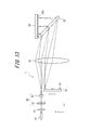
- FIG. 13 is a top view showing the configuration of the wavelength selective switch 1 according to the fourth embodiment of the present invention.
- the wavelength selective switch 1 includes an input / output unit 10, a microlens array 11, cylindrical lenses 12 and 13, a condensing lens 31, a transmissive dispersion element 32, a mirror (reflection element) 33, and a deflector 17. Is done.
- the input / output unit 10, the microlens array 11, and the cylindrical lenses 12 and 13 are the same optical elements as in the first embodiment.
- the condensing lens 31 has a distance in the z direction between the condensing lens 31 and the condensing point of the cylindrical lenses 12 and 13 and a distance from the center of the dispersion element 32 equal to the focal length of the condensing lens 31. Further, it is disposed between the cylindrical lens 13 and the dispersive element 32.
- the optical axis of the optical system composed of the microlens array 11 and the cylindrical lenses 12 and 13 in the xz plane and the optical axis of the condenser lens 31 are shifted in the second direction (x direction).
- the deflector 17 is a position where the condensing point by the cylindrical lenses 12 and 13 and the position in the z direction are substantially equal in a state where the deflecting element 18 faces the condensing lens 31 side. It is arranged shifted in the second direction (x direction) on the side through which the axis passes. That is, the distance between the condensing lens 31 and the deflecting element of the deflector 17 is also the focal length of the condensing lens 31.
- the dispersion element 32 and the mirror 33 form a dispersion portion having a so-called Littman-Metcalf type configuration. That is, the light diffracted (dispersed) by the dispersive element 32 is reflected by the mirror 33 and diffracted (dispersed) by the dispersive element 32 again. In this way, the dispersion angle can be increased by being diffracted (dispersed) by passing through the dispersive element twice.
- the mirror 33 has a function as a condensing position shift correction element having a refractive power in the dispersion direction of the dispersion element 32 in accordance with the position in the first direction (y direction) instead of the reflection surface 33a being a flat surface.
- the reflecting surface 33a does not have a refractive power in the first direction (y direction).
- the mirror 33 has a straight xz cross section when the first direction (y direction) of the reflecting surface 33a is at the same height as the optical axis, and the mirror 33 becomes negative as it deviates from the height position in the first direction (y direction). It can be configured to be a curved surface having refractive power.
- the input light input from any of the input / output ports 10a to 10c and 10e of the input / output unit 10 is converted into a parallel light beam by the corresponding microlens in the microlens array 11, and the cylindrical lens 12 and 13, after being condensed by the condensing lens 31, the light is dispersed into the light for each wavelength by the dispersive element 32, folded by the mirror 33, further dispersed by the dispersive element 32, and deflected by the condensing lens 31.
- the light is condensed on the deflecting element 18 of the vessel 17.
- the light for each wavelength is reflected by the deflecting element 18 at different angles for each wavelength, and the optical path until the light is reflected by the deflecting element 18 is folded and output to the input / output port 10 d of the input unit 10.
- the input light input from the input / output port that is separated from the optical axis has a position shift of the condensing position in the second direction (x direction) of the deflecting element 18, and the reflecting surface 33 a of the mirror 33. It is corrected by. Therefore, as in the first embodiment, the light of each wavelength dispersed by the dispersion element 32 is not dependent on the positions of the input / output ports 10a to 10c and 10e to which the input light is input, and the deflection element 18 Light can be condensed on the deflection element surface with high accuracy. Furthermore, since the optical system is folded using the mirror 33 and the apparatus is configured with a smaller number of lenses than in the first embodiment, the space required for mounting may be small, and the apparatus Can be miniaturized.
- the condensing position deviation correction element so that the input light input from the input / output port 10d is condensed on the deflection element surface of the deflection element 18 with high accuracy. 20 is preferably configured.
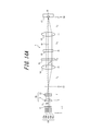
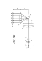
- (Fifth embodiment) 14A and 14B are a side view and a top view, respectively, showing the configuration of the wavelength selective switch 1 according to the fifth embodiment of the present invention.
- the condensing position deviation correction element 20 is arranged not between the microlens array 11 and the cylindrical lens 12 but between the lens 14 and the dispersion element 15 in the first embodiment. is there.
- the beam shaping optical system 25 is constituted by the cylindrical lenses 12 and 13. Since other configurations and operations are the same as those of the first embodiment, the same components are denoted by the same reference numerals and description thereof is omitted.
- the light of each wavelength dispersed by the dispersion element 15 is deflected by the deflection element 18 without depending on the position of the input / output port to which the input light is input.
- Light can be condensed with high accuracy on the element surface. Therefore, it is possible to suppress the occurrence of crosstalk and the reduction of the coupling efficiency of the output light to the output port due to the light of different wavelengths entering the same deflecting element, thereby improving the communication quality.
- the condensing position deviation correction element so that the input light input from the input / output port 10d is condensed on the deflection element surface of the deflection element 18 with high accuracy. 20 is preferably configured.
- (Sixth embodiment) 15A and 15B are a side view and a top view, respectively, showing the configuration of the wavelength selective switch 1 according to the sixth embodiment of the present invention.
- the beam shaping optical system 25 and the lens 14 are not provided in the first embodiment, and the condensing position deviation correction element 20 is disposed between the microlens array 11 and the dispersion element 15. is there.
- the input light input from the input / output ports 10 a to 10 c and 10 e is incident on the dispersive element 15 as a parallel light beam by the microlens array 11. Since other configurations and operations are the same as those of the first embodiment, the same components are denoted by the same reference numerals and description thereof is omitted.
- the beam shaping for forming an elliptical spot on the deflecting element 18 is not performed, but as in the first embodiment, the second direction ( It is possible to correct the deviation of the light collection position in the x direction). Therefore, the light for each wavelength dispersed by the dispersion element 15 can be condensed with high accuracy on the deflection element surface of the deflection element 18 without depending on the position of the input / output port to which the input light is input. . Therefore, it is possible to suppress the occurrence of crosstalk and the deterioration of the coupling efficiency to the output port due to light of different wavelengths entering the same deflecting element, thereby improving the communication quality.
- the condensing position deviation correction element so that the input light input from the input / output port 10d is condensed on the deflection element surface of the deflection element 18 with high accuracy. 20 is preferably configured.
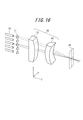
- FIG. 16 is a perspective view for explaining the configuration from the input / output port 10 of the wavelength selective switch 1 according to the seventh embodiment of the present invention to the vicinity of the primary condensing surface Sf and the beam passing therethrough.
- a condensing position deviation correction element 41 instead of the condensing position deviation correction element 20 and the cylindrical lens 13 in the first embodiment, a condensing position deviation correction element 41 having a different shape from the condensing position deviation correction element 20 is used. This is provided at a position where the cylindrical lens 13 in one embodiment is disposed.
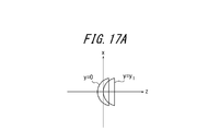
- FIG. 17A is a diagram showing the position and shape of a cross section on a plane parallel to the xz plane of the condensing position deviation correction element 41 of FIG.
- FIG. 17B is a cross-sectional view taken along the yz plane of the condensing position deviation correction element 41 of FIG.
- the cross section of the condensing position deviation correction element 41 parallel to the xz plane has an arc regardless of the height position from the optical axis in the first direction (y direction), for example, approximately half It has a circular shape.
- the semicircular cross-sectional shape shifts in the traveling direction of the input light (on the primary condensing surface Sf side) along the z-axis as the distance from the optical axis increases.
- the condensing position deviation correction element 41 has an input light whose cross section of the refracting surface orthogonal to the second direction (x direction) depends on the position in the first direction (y direction). It is inclined in the traveling direction (z direction). That is, the condensing position deviation correction element 41 has a shape in which both end portions in the y-axis direction protrude in the z-axis direction as compared to the central portion in the y-axis direction.
- the condensing position deviation correction element 41 is the same regardless of the distance in the first direction (y direction) from the optical axis.
- the refractive power in the direction 2 (x direction) is constant.
- the condensing position deviation correction element 41 adjusts the condensing position by shifting the refractive surface in the optical axis direction according to the distance from the optical axis. Since other configurations and operations are the same as those of the first embodiment, the same components are denoted by the same reference numerals and description thereof is omitted.
- the condensing position deviation correction element 41 that does not have a refractive power distribution in the second direction (x direction), similarly to the first embodiment, It is possible to correct the deviation of the light collection position in the second direction (x direction). Therefore, the light for each wavelength dispersed by the dispersion element 15 is collected with high accuracy on the deflection element surface of the deflection element 18 without depending on the positions of the input / output ports 10a to 10c and 10e to which the input light is input. Can be lighted. Therefore, it is possible to suppress the occurrence of crosstalk and the deterioration of the coupling efficiency to the output port due to the light of different wavelengths entering the same deflecting element 18 and improve the communication quality.
- the condensing position deviation correction element so that the input light input from the input / output port 10d is condensed on the deflecting element surface of the deflecting element 18 with high accuracy. 20 is preferably configured.
- FIG. 18 is a perspective view showing a part of the configuration of the wavelength selective switch according to the eighth embodiment of the present invention.
- the beams from the input / output ports 10a to 10e to the vicinity of the primary condensing surface Sf and the vicinity of the deflecting element 18 are shown.
- the condensing position deviation correction element 20 of the first embodiment is replaced with the condensing position deviation correction element 20d of FIG. 18, and is omitted in FIG.
- a deflector 17 including a lens 14, a dispersion element 15, a lens 16, and a deflection element 18 is disposed.
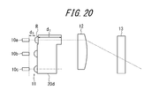
- the condensing position deviation correction element 20d of this optical system has no refractive power in both the first direction (y direction) and the second direction (x direction), and each of the input lights from the input / output ports 10a to 10e It is comprised so that the air conversion length of the optical path which passes may differ.
- the “air equivalent length” is a length represented by d / n when light travels through a medium having a refractive index n along a light path by a distance d.
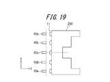
- the condensing position deviation correction element 20d has a thickness in the traveling direction (z direction) of input light that is thin in the central region in the first direction (y direction), and the first direction from the optical axis ( It is configured to become thicker with stepped steps as it goes away in the y direction).
- the regions where the light from the respective ports of the input / output ports 10a to 10e is incident have the same element thickness without straddling the steps.
- the surfaces facing the input / output ports are configured to be the same surface.
- the input light is assumed to be a Gaussian beam, the light beam has a spatially infinite spread.
- the region until the beam power becomes 1 / e 2 of the center is defined as the beam diameter.
- the condensing position deviation correction element 20d is made of a transparent material in the used wavelength band, and is configured using, for example, a semiconductor such as optical glass, resin, or silicon. In order to suppress the thickness of the element and provide a large correction effect, it is preferable to use a material having a large refractive index.
- the condensing position deviation correction element 20d By installing the condensing position deviation correction element 20d, the physical distance from the input / output port to the cylindrical lenses 12 and 13 can be kept unchanged while the air conversion length has port position dependency.
- the condensing position of the input light passing through the position away from the optical axis in the first direction (y direction) is shifted in the direction of the lens 14.
- the light of each wavelength dispersed by the dispersion element 15 is not dependent on the positions of the input / output ports 10a to 10c and 10e to which the input light is input, and the deflection element 18 Light can be condensed on the deflection element surface with high accuracy. Furthermore, since the condensing position deviation correction element 20d is composed of an element having no refractive power, high accuracy is not required for adjustment in the z-axis direction, and assembly can be facilitated.
- the microlens of the microlens array 11 and the condensing position deviation correction element 20d may be integrated.
- the beam shaping optical system 25 and the microlens array 11 may be integrated.
- the functional part of the microlens array 11 and the functional part of the condensing position deviation correction element 20d may be formed from one member, or the microlens and the condensing position deviation correction element manufactured individually may be joined. It may be formed.
- the device for reducing the noise by reflection of an interface is needed.
- the radius of curvature R of the array 11 may be set together.
- the light for each wavelength dispersed by the dispersive element 15 does not depend on the positions of the input / output ports 10a to 10c and 10e to which the input light is input, and is more accurate and free on the deflecting element surface of the deflecting element 18. It can be condensed at a degree.
- the correction effect in the first direction (y direction) and the correction effect in the second direction (x direction) can be designed in a more independent state.
- the air conversion length of the optical path does not necessarily have to be different for each input / output port. At least the air conversion length for the input / output port near the center of the optical axis and the input / output far from the optical axis. What is necessary is just to have at least 2 types of the air conversion length with respect to a port. In that case, when the light flux from the adjacent input / output port sandwiches the boundary where the air conversion length of the condensing position deviation correction element 20d changes, the interval between the input / output ports is made larger than the interval between the other ports. You may comprise. As a result, it is possible to prevent light incident from one input / output port from being separated by the boundary.
- the condensing position deviation correction element 20d in the present embodiment is not characterized in that the thickness of the element is different in the first direction (y direction), but in that the air conversion length of the optical path is different. It is. Therefore, the refractive index can be changed by changing the material constituting the condensing position deviation correction element 20d according to the position in the first direction while making the thickness of the element uniform in the first direction. good.
- the configuration of the above-described embodiment has been described by setting the installation position of the condensing position deviation correction element 20d to a place where an optimum effect can be obtained.
- the arrangement of the condensing position deviation correction element 20d is not limited to this, and if the incident light from each input / output port is arranged for each port, a correction effect can be obtained.
- the condensing position deviation correction element 20d and the cylindrical lens 12 are spaced apart from each other, but instead of this, the condensing position deviation correction element 20d is replaced with z.
- the converging position deviation correcting element 20d and the cylindrical lens 12 may be in contact with each other, or the converging position deviation correcting element 20d and the cylindrical lens 12 may be configured integrally. .
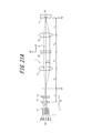
- (Ninth embodiment) 21A and 21B are diagrams showing the configuration of the wavelength selective switch according to the ninth embodiment of the present invention.
- This wavelength selective switch is the same as the wavelength selective switch according to the first embodiment shown in FIGS. 1A and 1B, but does not include the condensing position deviation correction element 20 in the beam shaping optical system 25, and the condensing position deviation occurs in the dispersive element 15 ′. It has a function of a correction element. That is, the dispersive element and the condensing position deviation correcting element in the present embodiment are configured as an integral unit.
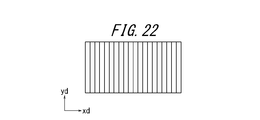
- FIG. 22 is a front view of a general dispersion element. This dispersive element has a diffraction grating, and the pitch of the diffraction grating has a regular pitch over the entire surface.
- the dispersion element 15 of the first embodiment has such a uniform pitch.
- FIG. 23 is a diagram showing a lattice of the dispersive element 15 ′ according to the present embodiment.
- the dispersive element 15 ' is divided into three in the yd direction, and the region a and the region c have the same lattice pitch.
- the pitch continuously changes along the second direction xd.
- the center region b is a lattice having the same pitch as in the first embodiment. The lattice in the central region b and the lattices in the regions a and b are discontinuous.
- FIG. 15 A perspective view of the dispersing element 15 'is shown in FIG.
- the height of the convex portion 15'a of the grating constituting the diffractive surface and the ratio of the width between the concave portion 15'b and the convex portion 15'a are optimized so as to maximize the diffracted light.
- the convex portion 15 ′ a may be configured by laminating a plurality of dielectrics so as to eliminate the difference in the amount of diffracted light depending on the polarization direction.
- the wavelength selective switch according to the present embodiment does not include the condensing position deviation correction element 20, and therefore, as illustrated in FIG.
- the light beam from the output port 10a is not condensed on the primary condensing surface Sf but is condensed on the dummy flat surface Sd separated by ⁇ z on the cylindrical lens 13 side.
- the primary condensing surface Sf and subsequent portions are shown in FIGS. 26A and 26B.
- Light rays from the input / output port 10a are indicated by solid lines, and light rays from the input / output port 10c are indicated by broken lines.
- Input light from the input / output port 10c passes almost on the axis of the optical system.
- This input light is condensed on the primary condensing surface Sf, becomes a parallel light beam along the optical axis by the lens 14 and is dispersed for each wavelength by the dispersive element 15 ′, and the light flux of each wavelength dispersed by the lens 16 is The light is condensed on the element surface (mirror surface) Sm of each deflection element 18 on the deflector 17.
- the input light from the input / output port 10a is focused on Sd which is ⁇ z away from the primary condensing surface Sf to the cylindrical lens 13 side. Incident at 15 ′.
- a position incident on the dispersion element 15 ' is a position away from the optical axis in the yd direction, that is, a region c in FIG.
- the grating in the region c has refractive power by changing the pitch interval along the xd direction, and disperses the incident light beam as a convergent light beam into light of each wavelength as a parallel light beam. Therefore, similarly to the light flux from the input / output port 10 c, the dispersed light flux of each wavelength is condensed by the lens 16 on the element surface (mirror surface) of each deflection element 18 on the deflector 17. As shown in the top view of FIG. 26B, when viewed from the first direction (y-direction), after being dispersed by the dispersive element 15 ′, neither the light beam from the input / output port 10c nor the light beam from the input / output port 10a. Looks like they overlap. The light beam reflected by the element surface Sm of each deflection element 18 returns to the reverse direction of the optical path described above, and is condensed and output to the input / output port 10d.
- the lattice becomes discontinuous where the characteristics of the lattice change, such as the boundary between the region a and the region b.
- the interval between the input / output ports through which the light flux passes above and below the boundary is set to other boundaries. It is preferable that the distance between the input and output ports be slightly larger.
- the diffractive surface of the dispersive element 15 ′ is divided into three regions in the direction in which the grating extends. However, a region c far from the central region is assumed to have two input / output ports 10a and 10b, respectively.
- the lattice pitch is optimized in accordance with ⁇ z of the input / output port 10a that is outside the outermost axis
- the light is condensed at the deflection element 18 of the input / output port 10b inside the input / output port 10a that is outside the outermost axis.
- the position may be overcorrected. Therefore, by increasing the number of divided regions and optimizing the grating pitch according to ⁇ z of each input / output port, the light collection positions of the light beams from all the input / output ports 10a to 10c and 10e are The distance to the element surface Sm at the deflection element 18 can be reduced.
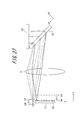
- FIG. 27 is a top view showing a configuration and an optical path from the vicinity of the primary condensing surface of the wavelength selective switch to the deflector according to the tenth embodiment of the present invention.
- This wavelength selective switch is a wavelength selective switch having a Littman-Metcalf-type dispersion unit according to the fourth embodiment shown in FIG. 13, and does not include a condensing position shift correction element in the beam shaping optical system 25.
- the element 32 ′ is configured integrally with the condensing position deviation correction element.
- the dispersive element 32 ′ has a discontinuous lattice in the yd direction and the pitch interval in the xd direction is unequal, as in the dispersive element 15 ′ of the ninth embodiment. Since other configurations are the same as those of the fourth embodiment, the same components are denoted by the same reference numerals, and description thereof is omitted.
- the light beam from the input / output port 10a is indicated by a solid line
- the light beam from the input / output port 10c is indicated by a broken line.
- the light flux from the input / output port 10c is condensed on the primary condensing surface Sf. After condensing, the light beam diverging from Sf becomes a parallel light beam by the condensing lens 31, and is dispersed into light of each wavelength by the dispersive element 32 '.
- the light for each wavelength is reflected by the mirror 33, further dispersed by the dispersion element 32 ′, and enters the condenser lens 31.
- the condensing lens 31 condenses the dispersed parallel light flux of each wavelength on the deflection surface (mirror surface) Sm of the deflection element 18 of the deflector 17.
- the light flux from the input / output port 10a is condensed on the surface Sd closer to the input / output port than the primary condensing surface Sf, so that it is converted into a light flux that converges a little more than the parallel light flux by the condenser lens 31.
- the dispersive element 32 ' is divided into a central region b and an outer region a and a region c in the yd direction, like the dispersive device 15' shown in FIG.
- the light beam from the input / output port 10a passes through the outer region c.
- the outer region c has a refractive power that disperses a slightly converged light beam into a light beam for each wavelength at unequal pitches and converts the light of each wavelength into a divergence direction so as to be close to a parallel light beam. ing.
- the light beams having these wavelengths are reflected by the mirror 33 and are incident on the dispersion element 32 'again.
- the incident light flux is further dispersed and further converted into a divergence direction to become a parallel light flux dispersed at each wavelength.
- the condensing lens 31 condenses the parallel light flux dispersed in each wavelength on the deflecting element surface Sm (mirror surface) of the deflecting element 18 of the deflector 17.
- the light reflected by the deflecting element surface (mirror surface) Sm returns in the reverse direction along the above-described optical path and is collected on the exit surface of the input / output port 10d.
- the horizontal axis of FIG. 28 shows the coordinates in the xd direction of FIG. 27, and the vertical axis shows the pitch value normalized with the pitch of the central region b of the deflection element 32 'taken as 1.
- the broken line is a graph for the center region b, and the solid line is a graph for the region a and the region c.
- the pitch of the center region b is set at equal intervals, the value of the horizontal axis of the broken line graph is 1 regardless of the coordinate xd.
- the pitch is slightly narrowed in the positive direction of the coordinate xd.
- FIG. 29 is a graph showing a distance ⁇ z ′ between the deflecting element surface (mirror surface) Sm and the condensing position Sm ′ of the light beam from each port.
- the horizontal axis indicates the relative value of the port height from the optical axis, and the port height of the input / output port 10a is 1.
- the vertical axis indicates the relative value of ⁇ z ′.
- the broken line is ⁇ z ′ calculated for the case of using a normal grating having an equally spaced pitch, and the solid line indicates the value of ⁇ z ′ when the dispersive element 32 ′ according to the present embodiment is used. ing.
- the vertical axis represents 1 as the value of ⁇ z ′ for the input / output port 10a when using dispersive elements having equal pitches.
- Input light incident from the input / output port 10a passes through the region c of the dispersion element 32 ', and input light incident from the input / output ports 10b and 10c passes through the central region b of the dispersion element 32'. It can be seen that by using the dispersive element 32 ′ of the present embodiment, ⁇ z ′ of the light beam incident from the input / output port 10 a can be reduced.
- the dispersion element including the condensing position deviation correction function used in the present embodiment can be manufactured by the same method as the conventional dispersion element only by changing the mask pattern, and the cost is hardly changed. .
- the light for each wavelength dispersed by the dispersion element 32 ′ is not dependent on the positions of the input / output ports 10a to 10c and 10e to which the input light is input. Insertion loss caused by a decrease in coupling efficiency regardless of the input / output port because it can be condensed with high accuracy at a position optically conjugate with the exit surface of the input / output port 10d functioning as an output port. Therefore, it is possible to provide a wavelength selective switch with a small amount.
- FIG. 30 is a perspective view showing a part of the configuration of the wavelength selective switch according to the eleventh embodiment of the present invention.
- FIG. 30 shows beams from the input / output ports 10a to 10e to the vicinity of the condensing point and in the vicinity of the deflecting element 18 ′.
- the deflection element 18 ′ the light for each wavelength from each input port is deflected on the deflection surface of the deflection element 18 ′.
- a mirror element whose center of rotation is shifted to the first direction side is used, and the condensing position deviation correction element 20 is replaced with the condensing position deviation correction element 20e of FIG.
- a deflector 17 including a lens 14, a dispersion element 15, a lens 16, and a deflection element 18 ′ is disposed in the subsequent stage, as in the wavelength selective switch 1 of the first embodiment. Yes.
- the same components as those in the first embodiment are denoted by the same reference numerals, and description thereof is omitted.
- the deflector 17 is, for example, a MEMS mirror array
- the deflection element 18 ′ is an element including a micromirror that constitutes the MEMS mirror array.
- the rotation axis when changing the inclination of the deflection element 18 ′ in the yz plane in FIG. 1A is the first relative to the position where the light beam dispersed for each wavelength is deflected. It is shifted to the direction side.
- Such a mirror arrangement configuration is due to a requirement for securing a space for electrode arrangement when the pitch of the MEMS mirror array is reduced, and a mirror configuration that allows easy manufacture of a cantilever type.
- the deflection element surface Sm is not a fixed surface, as indicated by Sma and Smb in FIG.
- FIGS. 31A, 31B and 31C are viewed from the xz cross section in the upper stage, and are viewed from the yz cross section in the lower stage.
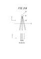
- FIG. 31A is a diagram schematically showing the displacement of the deflection element surface Sm when the micro mirror 52 of the deflection element 18 ′ is rotated with respect to the rotation shaft 51. Since the rotation axis 51 of the micro mirror 52 is shifted from the optical axis O of the lens 16 in the first direction (y direction), the micro mirror 52 is changed to a different deflection angle in order to change the combination of input / output ports. , Sma, Smb, and Smc, the deflection element surface Sm is displaced (d1 and d2 in the figure) with a deflection angle dependency in the z-axis direction.
- the deflection angle of the micromirror 18 ′ serving as Sma, Smb, and Smc represents the state in which the input / output ports 10a and 10d, 10b and 10d, and 10e and 10d are optically coupled, respectively. .
- FIG. 31B is a diagram schematically showing a light beam in the vicinity of the deflecting element 18 ′ when the light beams incident from the input / output ports 10a, 10b and 10e are fixedly focused on the position of the deflecting element surface Smb. is there. That is, the light beam is shown when the displacement of the deflection element surface Sm due to the rotation of the mirror surface is not taken into consideration.
- L 1 , L 2, and L 3 indicate light beams incident from the input / output ports 10 a, 10 b, and 10 e, respectively.
- the lower stage schematically shows the outer shapes of these light beams.
- L 1 ', L 2' and L 3 ', respectively, L 1, L 2 and L 3 indicates a light beam is reflected toward the output port 10d by the micro mirror 52.
- the micro-mirror 18 'the position of the is in Smb
- the light beam L 2 from the input port 10b is reflected by the micromirror 52
- the light beam L 2' becomes . Since the condensing point on the deflecting element surface Smb is arranged at a conjugate position with the input / output surface of the input / output port 10d, the reflected light beam L 2 ′ is efficiently coupled to the input / output port 10d.
- the condensing positions of the light fluxes from the input / output ports 10a, 10b, and 10e are set as shown in FIG.
- the light beam L 3 from output port 10e is configured to have a converging position (Gaussian image plane) to the point P 1 of the front of the deflection element surface Sma.
- the condensing position of the light emitted from the input / output port 10d acting as the output port (matches Smb) and the condensing position P 1 of the light incident from the input / output port 10e acting as the input port. are preferably formed at positions symmetrical with respect to the deflection element surface Sma in the z-axis direction.
- the condensing position (Gauss image plane) of the light emitted from each of the input / output ports 10e and 10d can be matched through reflection by the deflecting element 18 ′, and can be efficiently combined.
- the light beam L 3 from the input / output port 10e is reflected by the deflection element surface Sma, but the reflected light beam L 3 ′ is the same as the light that diverges after being collected by the deflection element surface Smb. It is efficiently coupled to the output port 10d.
- the input / output ports 10a and 10d are optically coupled. That is, the light beam L 1 incident from input port 10a is configured to have the condensing position from the deflection element surface Smc to the distance d2 position P 2 advanced.
- the light condensing position of the light from the input / output port 10a and the light condensing position of the light from the input / output port 10e are reversed in the direction shifted from Sm (Smb) which is a fixed point in space. .
- the condensing position deviation correction element 20e of the present embodiment is configured as follows.
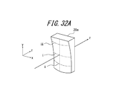
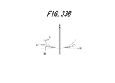
- FIG. 32A is a perspective view showing an example of a condensing position deviation correction element in consideration of the displacement of the deflection element surface Sm.
- FIG. 32B is a diagram for explaining the shape of the refracting surface of the condensing position deviation correcting element 20e in FIG. 32A.
- the condensing position deviation correction element 20e is made of a light transmissive member such as glass.
- the front side is a curved surface having refractive power
- the back side is a flat surface.
- Each of i, ii, and iii indicates the cross-sectional shape of the refracting surface of the condensing position deviation correction element 20e by a plane parallel to the xz plane having a different y-direction position.
- the condensing position deviation correction element 20e has substantially no refractive power in the first direction (y direction). Further, the condensing position deviation correction element 20e has different refractive power in the second direction (x direction) depending on the position in the first direction (y direction).
- the refractive power in the second direction (x direction) is close to 0 (cross section iii), and the first from the end In the negative direction (y direction), the closer to the center position in the negative direction, the larger the positive refractive power in the second direction (x direction) (cross section i). Furthermore, as the distance from the center position is negative in the first direction (y direction), the second direction (x direction) has a smaller positive refractive power (cross section ii). Compared to the case where the first direction (y direction) is separated in the positive direction, the refractive power when the same distance is separated in the negative direction is small.
- the condensing position of the light beam passing through the position away from the optical axis in the first direction (y direction) is shifted in the direction of the lens 14 asymmetrically in the first direction (y direction). That is, the condensing position deviation correction element 20e has an asymmetric structure in the first direction (y direction).
- the center position in the second direction (x direction) is a position through which the synthetic lens of the cylindrical lenses 12 and 13 and the optical axis of the lens 14 pass.
- the shape of the above-described condensing position deviation correction element 20e is an example, and the same effect can be obtained even if a condensing position deviation correction element having another shape is used.
- the refractive power in the second direction (x direction) is 0, and from this center position in the first direction (y direction) in the positive and negative directions.
- the shape has a larger negative refractive power in the second direction (x direction) and a smaller refractive power in the case of moving away in the negative direction than in the case of moving away in the positive direction. You can also. In this case, it is necessary to change the curvatures of the cylindrical lenses 12 and 13 according to the shape of the condensing position deviation correction element 20e.
- the refractive power of the condensing position deviation correcting element 20e can be any of monotonically decreasing, monotonically increasing, or a function having one or more inflection points in the y direction.
- the refracting surface of the condensing position deviation correction element 20e is formed of a curved surface whose curvature changes smoothly, whereas the refracting surface of the condensing position deviation correction element 20f includes the input / output ports 10a to 10c and Corresponding to the incident position of the input light from 10e in the first direction (y direction), a part of cylindrical surfaces having different curvatures in the second direction (x direction) are combined.
- each cylindrical surface is arranged so that the refracting surface forms a straight line in the yz plane including the z axis.
- a step is provided at the boundary of the cylindrical refracting surface corresponding to each of the different input / output ports 10a to 10e.
- the refracting surface may not be a straight line in the yz plane including the z axis.
- the cylindrical refracting surfaces corresponding to the different input / output ports 10a to 10e may be formed by stacking concentric cylinders. Also in this case, uniform refractive power can be exerted in the second direction (x direction) on the input light fluxes of the respective input lights from the input / output ports 10a to 10c and 10e.
- the wavelength selective switch according to the present embodiment, even when the element surface Sm of the deflection element 18 is displaced according to the combination of the input / output ports 10a to 10e to be selected, Similar to the embodiment, the input / output ports functioning as output ports without depending on the positions of the input / output ports 10a to 10c and 10e to which the input light is input, for the light of each wavelength dispersed by the dispersion element 15
- the light can be condensed with high accuracy at a position optically conjugate with the 10d emission surface.
- the condensing position deviation correction elements 20e and 20f have an asymmetric refractive power with respect to the optical axis in the first direction (y direction), the micromirror whose rotation center is separated from the center of the reflecting surface.
- the light converging position can be optimally adjusted with a high degree of freedom even with respect to the deflection element.
- the condensing position deviation correction element 20 arranged near the input / output ports 10a to 10e is replaced with the condensing position deviation correction element 20e.
- the condensing position deviation correcting element is arranged so that the condensing position of light from the input port is The same effect can be obtained by using an asymmetric structure so as to be conjugate with the position of the output port.
- the lattice characteristic of the dispersive element 18 ′ is axisymmetric in the yd direction, but the lattice characteristic may be configured asymmetrically. That is, the lattice characteristics may be different in all the regions a, b, and c.
- the dispersive element has a dispersive function and a converging position deviation correction function.
- the light of each wavelength dispersed by the dispersion element can be optically input to the input / output port 10d and the input / output surface without depending on the positions of the input / output ports 10a to 10c and 10e to which the input light is input. Light can be condensed with high accuracy at a conjugate position.
- the input port and the output port may be configured such that a plurality of common input / output ports are provided and the input port and the output port can be switched as appropriate.
- the input port and the output port have their end faces arranged in series, but may be separated and arranged at separate positions.
- the condensing position deviation correction element of the present invention corrects input light so as to form a spot having the narrowest width in the second direction (x direction) on the deflection element surface. Even if the width in the second direction (x direction) does not become the minimum value, if the width of the spot in the second direction (x direction) is smaller than that in the case where no condensing position deviation correction element is provided, the present The communication quality improvement effect according to the invention can be obtained. Therefore, the scope of the present invention includes a case where the spot in the second direction (x direction) does not become the minimum value as long as such an effect is obtained.
- the vertical direction orthogonal to the optical axis direction (z direction) of the input light output from the input / output port is the first direction (y direction), and the horizontal direction is the second direction (x direction).
- the first direction (y direction) is not limited to the vertical direction
- the second direction (x direction) is not limited to the horizontal direction.
- the first direction (y direction) and the second direction (x direction) may be two directions orthogonal to the traveling direction of the input light and orthogonal to each other.
- the beam shaping optical system includes a cylindrical lens having a refractive power in a first direction (y direction) and a cylindrical lens having a refractive power in a second direction (x direction) orthogonal to the first direction (y direction). It is not limited to a combination with a lens.
- a cylindrical lens having a refractive power in the first direction (y direction) a lens having a refractive power in at least the first direction (y direction), for example, a spherical lens is used, and a cylindrical lens is used in the subsequent stage.
- a lens can also be arranged.
- an elliptical beam waist can be formed at the condensing position.
- a Fresnel-shaped lens linear Fresnel lens
- a Fresnel-shaped lens linear Fresnel lens
- the shape of the condensing position deviation correction element exemplified in each embodiment is merely an example.
- the condensing position deviation correction element disposed in the beam shaping optical system is not limited to the form in which the refracting surface is on the input unit side, and the surface or both surfaces on the dispersing element side may be configured as a refracting surface.
- the deflecting unit is not limited to the MEMS mirror array, and may be configured using a liquid crystal element or an optical crystal.
- the lens 14 may have the same function as the condensing position deviation correction element 20. In this case, the surface having the correction function may or may not have refractive power in the first direction (y direction).
- each single member functions as a condensing position deviation correction element.
- a plurality of members may function as a condensing position deviation correction element. In this case, it is possible to substantially improve the yield of the members by selecting the respective members so as to cancel each other the variation in the correction force as the condensing position deviation correction element caused by the manufacturing variation of the respective members. Is possible.
Landscapes
- Physics & Mathematics (AREA)
- Engineering & Computer Science (AREA)
- Computer Networks & Wireless Communication (AREA)
- General Physics & Mathematics (AREA)
- Optics & Photonics (AREA)
- Mechanical Light Control Or Optical Switches (AREA)
- Optical Modulation, Optical Deflection, Nonlinear Optics, Optical Demodulation, Optical Logic Elements (AREA)
Abstract
L'invention concerne un commutateur sélectif en longueur d'onde (1) comprenant au moins un port d'entrée (10a-10c et 10e), un élément dispersif afin de disperser la lumière incidente multiplexée en longueur d'onde qui est incidente depuis les ports d'entrée (10a-10c et 10e) en lumière de chaque longueur d'onde, un élément de focalisation (16) afin de focaliser la lumière de chaque longueur d'onde dispersée par l'élément dispersif (15), un déflecteur (17) comportant un élément de déflection (18) qui dévie la lumière de chaque longueur d'onde focalisée par l'élément de focalisation (16), et au moins un port de sortie (10d) qui émet, en qualité de lumière de sortie, la lumière de chaque longueur d'onde déviée par le déflecteur (17). Dans l'élément dispersif susmentionné ou dans le trajet optique entre les ports d'entrée/sortie (10a-10e) et l'élément dispersif (15) de ce commutateur sélectif en longueur d'onde (1), un élément de correction d'erreur de position de focale (20) est utilisé afin de corriger une erreur de la position de focale de la lumière à chaque longueur d'onde par rapport à l'élément de déflection (18) due à l'agencement des ports d'entrée et de sortie (10a-10c et 10e).
Priority Applications (1)
| Application Number | Priority Date | Filing Date | Title |
|---|---|---|---|
| US13/497,105 US8634129B2 (en) | 2011-02-10 | 2012-01-30 | Wavelength selective switch |
Applications Claiming Priority (4)
| Application Number | Priority Date | Filing Date | Title |
|---|---|---|---|
| JP2011-027744 | 2011-02-10 | ||
| JP2011027744 | 2011-02-10 | ||
| JP2011-259557 | 2011-11-28 | ||
| JP2011259557A JP2012181498A (ja) | 2011-02-10 | 2011-11-28 | 波長選択スイッチ |
Publications (1)
| Publication Number | Publication Date |
|---|---|
| WO2012108139A1 true WO2012108139A1 (fr) | 2012-08-16 |
Family
ID=46638367
Family Applications (1)
| Application Number | Title | Priority Date | Filing Date |
|---|---|---|---|
| PCT/JP2012/000575 Ceased WO2012108139A1 (fr) | 2011-02-10 | 2012-01-30 | Commutateur sélectif en longueur d'onde |
Country Status (3)
| Country | Link |
|---|---|
| US (1) | US8634129B2 (fr) |
| JP (1) | JP2012181498A (fr) |
| WO (1) | WO2012108139A1 (fr) |
Cited By (1)
| Publication number | Priority date | Publication date | Assignee | Title |
|---|---|---|---|---|
| CN103676009A (zh) * | 2012-09-07 | 2014-03-26 | 古河电气工业株式会社 | 光开关 |
Families Citing this family (12)
| Publication number | Priority date | Publication date | Assignee | Title |
|---|---|---|---|---|
| US9188831B2 (en) | 2012-02-17 | 2015-11-17 | Alcatel Lucent | Compact wavelength-selective cross-connect device having multiple input ports and multiple output ports |
| US9369783B2 (en) * | 2012-02-17 | 2016-06-14 | Alcatel Lucent | Wavelength-selective cross-connect device having astigmatic optics |
| JP5692865B2 (ja) * | 2012-04-11 | 2015-04-01 | 独立行政法人産業技術総合研究所 | 波長クロスコネクト装置 |
| JP6119761B2 (ja) * | 2012-10-16 | 2017-04-26 | 住友電気工業株式会社 | 光路制御装置 |
| WO2014153455A1 (fr) * | 2013-03-20 | 2014-09-25 | Nistica, Inc. | Commutateur sélectif de longueurs d'onde employant un dispositif lcos et offrant une réduction de diaphonie |
| US9372311B2 (en) * | 2013-09-18 | 2016-06-21 | Sumitomo Electric Industries, Ltd. | Wavelength selective switch |
| JP6383166B2 (ja) * | 2014-03-28 | 2018-08-29 | 株式会社Screenホールディングス | 光照射装置および描画装置 |
| ES2688210T3 (es) * | 2014-04-22 | 2018-10-31 | Huawei Technologies Co., Ltd | Aparato y procedimiento de comunicaciones ópticas |
| US10133187B2 (en) | 2015-05-29 | 2018-11-20 | SCREEN Holdings Co., Ltd. | Light irradiation apparatus and drawing apparatus |
| US10042121B1 (en) * | 2017-03-28 | 2018-08-07 | Nistica, Inc. | Toroidal micro lens array for use in a wavelength selective switch |
| US10416383B2 (en) * | 2017-07-20 | 2019-09-17 | The Board Of Trustees Of The University Of Illinois | Spatial control of the optical focusing properties of photonic nanojets |
| CN117031636B (zh) * | 2023-10-08 | 2024-02-09 | 华中科技大学 | 一种Twin结构的波长选择开关及智能光网络器件 |
Citations (4)
| Publication number | Priority date | Publication date | Assignee | Title |
|---|---|---|---|---|
| JP2006276216A (ja) * | 2005-03-28 | 2006-10-12 | Fujitsu Ltd | 光スイッチ |
| JP2008040447A (ja) * | 2006-07-14 | 2008-02-21 | Fujitsu Ltd | レンズアレイを用いた光学装置 |
| JP2008139785A (ja) * | 2006-12-05 | 2008-06-19 | Fujitsu Ltd | レンズ調節方法、レンズ調節装置および光スイッチ |
| JP2008242281A (ja) * | 2007-03-28 | 2008-10-09 | Fujitsu Ltd | 光波長選択スイッチおよび光波長選択スイッチの調節方法 |
Family Cites Families (4)
| Publication number | Priority date | Publication date | Assignee | Title |
|---|---|---|---|---|
| US6657770B2 (en) * | 2001-06-22 | 2003-12-02 | Lucent Technologies Inc. | Programmable optical multiplexer/demultiplexer |
| US7702194B2 (en) * | 2006-11-07 | 2010-04-20 | Olympus Corporation | Beam steering element and associated methods for manifold fiberoptic switches |
| JP5006704B2 (ja) | 2007-06-18 | 2012-08-22 | Nttエレクトロニクス株式会社 | 波長選択スイッチ |
| JP2010134027A (ja) | 2008-12-02 | 2010-06-17 | Olympus Corp | 波長選択スイッチ |
-
2011
- 2011-11-28 JP JP2011259557A patent/JP2012181498A/ja active Pending
-
2012
- 2012-01-30 WO PCT/JP2012/000575 patent/WO2012108139A1/fr not_active Ceased
- 2012-01-30 US US13/497,105 patent/US8634129B2/en active Active
Patent Citations (4)
| Publication number | Priority date | Publication date | Assignee | Title |
|---|---|---|---|---|
| JP2006276216A (ja) * | 2005-03-28 | 2006-10-12 | Fujitsu Ltd | 光スイッチ |
| JP2008040447A (ja) * | 2006-07-14 | 2008-02-21 | Fujitsu Ltd | レンズアレイを用いた光学装置 |
| JP2008139785A (ja) * | 2006-12-05 | 2008-06-19 | Fujitsu Ltd | レンズ調節方法、レンズ調節装置および光スイッチ |
| JP2008242281A (ja) * | 2007-03-28 | 2008-10-09 | Fujitsu Ltd | 光波長選択スイッチおよび光波長選択スイッチの調節方法 |
Cited By (2)
| Publication number | Priority date | Publication date | Assignee | Title |
|---|---|---|---|---|
| CN103676009A (zh) * | 2012-09-07 | 2014-03-26 | 古河电气工业株式会社 | 光开关 |
| JP2014067004A (ja) * | 2012-09-07 | 2014-04-17 | Furukawa Electric Co Ltd:The | 光スイッチ |
Also Published As
| Publication number | Publication date |
|---|---|
| JP2012181498A (ja) | 2012-09-20 |
| US8634129B2 (en) | 2014-01-21 |
| US20130038917A1 (en) | 2013-02-14 |
Similar Documents
| Publication | Publication Date | Title |
|---|---|---|
| WO2012108139A1 (fr) | Commutateur sélectif en longueur d'onde | |
| US8391654B2 (en) | Wavelength selection switch | |
| JP5040842B2 (ja) | 波長選択スイッチ | |
| JP6244721B2 (ja) | 波長多重伝送装置の製造方法 | |
| US20140072302A1 (en) | Optical switch | |
| US20140268305A1 (en) | Wavelength selective switch | |
| JP5935465B2 (ja) | 光学装置 | |
| US8208771B2 (en) | Optical switch | |
| JP3973944B2 (ja) | 光接続モジュール及び赤外光用光学系 | |
| JP2013152414A (ja) | 波長選択スイッチ | |
| EP2570831B1 (fr) | Dispositif de traitement optique | |
| US9671576B1 (en) | CWDM transceiver module | |
| US8243372B2 (en) | Optical apparatus and optical transmission apparatus | |
| US9454002B2 (en) | Wavelength selection switch | |
| WO2012115077A1 (fr) | Commutateur de sélection de longueur d'onde | |
| JP2013142875A (ja) | 波長選択スイッチ | |
| JP5546410B2 (ja) | 光学部材、これを用いた光通信モジュール及び調芯方法 | |
| JP2012145373A (ja) | 分光装置及びそれを用いた波長選択スイッチ | |
| US20050237642A1 (en) | Decentering optical system, optical transmitting device, optical receiving device, and optical system | |
| WO2012108189A1 (fr) | Commutateur sélectif en longueur d'onde et unité optique pour commutateur sélectif en longueur d'onde | |
| JP2012181497A (ja) | 波長選択スイッチ | |
| JP2005326603A (ja) | 光通信装置 | |
| JP2012133191A (ja) | 光学装置 | |
| JP2012203136A (ja) | 波長選択スイッチ | |
| JP2012173720A (ja) | 波長選択スイッチ |
Legal Events
| Date | Code | Title | Description |
|---|---|---|---|
| WWE | Wipo information: entry into national phase |
Ref document number: 13497105 Country of ref document: US |
|
| 121 | Ep: the epo has been informed by wipo that ep was designated in this application |
Ref document number: 12744356 Country of ref document: EP Kind code of ref document: A1 |
|
| NENP | Non-entry into the national phase |
Ref country code: DE |
|
| 122 | Ep: pct application non-entry in european phase |
Ref document number: 12744356 Country of ref document: EP Kind code of ref document: A1 |