WO2012108301A1 - Substrat à matrice active, panneau d'affichage et dispositif d'affichage - Google Patents
Substrat à matrice active, panneau d'affichage et dispositif d'affichage Download PDFInfo
- Publication number
- WO2012108301A1 WO2012108301A1 PCT/JP2012/052107 JP2012052107W WO2012108301A1 WO 2012108301 A1 WO2012108301 A1 WO 2012108301A1 JP 2012052107 W JP2012052107 W JP 2012052107W WO 2012108301 A1 WO2012108301 A1 WO 2012108301A1
- Authority
- WO
- WIPO (PCT)
- Prior art keywords
- layer
- active matrix
- matrix substrate
- drain electrode
- electrode
- Prior art date
- Legal status (The legal status is an assumption and is not a legal conclusion. Google has not performed a legal analysis and makes no representation as to the accuracy of the status listed.)
- Ceased
Links
Images


Classifications
-
- H—ELECTRICITY
- H10—SEMICONDUCTOR DEVICES; ELECTRIC SOLID-STATE DEVICES NOT OTHERWISE PROVIDED FOR
- H10D—INORGANIC ELECTRIC SEMICONDUCTOR DEVICES
- H10D86/00—Integrated devices formed in or on insulating or conducting substrates, e.g. formed in silicon-on-insulator [SOI] substrates or on stainless steel or glass substrates
- H10D86/40—Integrated devices formed in or on insulating or conducting substrates, e.g. formed in silicon-on-insulator [SOI] substrates or on stainless steel or glass substrates characterised by multiple TFTs
- H10D86/60—Integrated devices formed in or on insulating or conducting substrates, e.g. formed in silicon-on-insulator [SOI] substrates or on stainless steel or glass substrates characterised by multiple TFTs wherein the TFTs are in active matrices
-
- H—ELECTRICITY
- H10—SEMICONDUCTOR DEVICES; ELECTRIC SOLID-STATE DEVICES NOT OTHERWISE PROVIDED FOR
- H10D—INORGANIC ELECTRIC SEMICONDUCTOR DEVICES
- H10D30/00—Field-effect transistors [FET]
- H10D30/60—Insulated-gate field-effect transistors [IGFET]
- H10D30/67—Thin-film transistors [TFT]
- H10D30/6729—Thin-film transistors [TFT] characterised by the electrodes
-
- H—ELECTRICITY
- H10—SEMICONDUCTOR DEVICES; ELECTRIC SOLID-STATE DEVICES NOT OTHERWISE PROVIDED FOR
- H10D—INORGANIC ELECTRIC SEMICONDUCTOR DEVICES
- H10D30/00—Field-effect transistors [FET]
- H10D30/01—Manufacture or treatment
- H10D30/021—Manufacture or treatment of FETs having insulated gates [IGFET]
- H10D30/031—Manufacture or treatment of FETs having insulated gates [IGFET] of thin-film transistors [TFT]
- H10D30/0312—Manufacture or treatment of FETs having insulated gates [IGFET] of thin-film transistors [TFT] characterised by the gate electrodes
- H10D30/0316—Manufacture or treatment of FETs having insulated gates [IGFET] of thin-film transistors [TFT] characterised by the gate electrodes of lateral bottom-gate TFTs comprising only a single gate
-
- H—ELECTRICITY
- H10—SEMICONDUCTOR DEVICES; ELECTRIC SOLID-STATE DEVICES NOT OTHERWISE PROVIDED FOR
- H10D—INORGANIC ELECTRIC SEMICONDUCTOR DEVICES
- H10D30/00—Field-effect transistors [FET]
- H10D30/01—Manufacture or treatment
- H10D30/021—Manufacture or treatment of FETs having insulated gates [IGFET]
- H10D30/031—Manufacture or treatment of FETs having insulated gates [IGFET] of thin-film transistors [TFT]
- H10D30/0321—Manufacture or treatment of FETs having insulated gates [IGFET] of thin-film transistors [TFT] comprising silicon, e.g. amorphous silicon or polysilicon
-
- H—ELECTRICITY
- H10—SEMICONDUCTOR DEVICES; ELECTRIC SOLID-STATE DEVICES NOT OTHERWISE PROVIDED FOR
- H10D—INORGANIC ELECTRIC SEMICONDUCTOR DEVICES
- H10D30/00—Field-effect transistors [FET]
- H10D30/60—Insulated-gate field-effect transistors [IGFET]
- H10D30/67—Thin-film transistors [TFT]
- H10D30/6729—Thin-film transistors [TFT] characterised by the electrodes
- H10D30/6737—Thin-film transistors [TFT] characterised by the electrodes characterised by the electrode materials
- H10D30/6739—Conductor-insulator-semiconductor electrodes
-
- H—ELECTRICITY
- H10—SEMICONDUCTOR DEVICES; ELECTRIC SOLID-STATE DEVICES NOT OTHERWISE PROVIDED FOR
- H10D—INORGANIC ELECTRIC SEMICONDUCTOR DEVICES
- H10D30/00—Field-effect transistors [FET]
- H10D30/60—Insulated-gate field-effect transistors [IGFET]
- H10D30/67—Thin-film transistors [TFT]
- H10D30/674—Thin-film transistors [TFT] characterised by the active materials
- H10D30/6741—Group IV materials, e.g. germanium or silicon carbide
- H10D30/6743—Silicon
-
- H—ELECTRICITY
- H10—SEMICONDUCTOR DEVICES; ELECTRIC SOLID-STATE DEVICES NOT OTHERWISE PROVIDED FOR
- H10D—INORGANIC ELECTRIC SEMICONDUCTOR DEVICES
- H10D30/00—Field-effect transistors [FET]
- H10D30/60—Insulated-gate field-effect transistors [IGFET]
- H10D30/67—Thin-film transistors [TFT]
- H10D30/674—Thin-film transistors [TFT] characterised by the active materials
- H10D30/6755—Oxide semiconductors, e.g. zinc oxide, copper aluminium oxide or cadmium stannate
-
- H—ELECTRICITY
- H10—SEMICONDUCTOR DEVICES; ELECTRIC SOLID-STATE DEVICES NOT OTHERWISE PROVIDED FOR
- H10D—INORGANIC ELECTRIC SEMICONDUCTOR DEVICES
- H10D64/00—Electrodes of devices having potential barriers
- H10D64/60—Electrodes characterised by their materials
- H10D64/62—Electrodes ohmically coupled to a semiconductor
-
- H—ELECTRICITY
- H10—SEMICONDUCTOR DEVICES; ELECTRIC SOLID-STATE DEVICES NOT OTHERWISE PROVIDED FOR
- H10D—INORGANIC ELECTRIC SEMICONDUCTOR DEVICES
- H10D86/00—Integrated devices formed in or on insulating or conducting substrates, e.g. formed in silicon-on-insulator [SOI] substrates or on stainless steel or glass substrates
- H10D86/40—Integrated devices formed in or on insulating or conducting substrates, e.g. formed in silicon-on-insulator [SOI] substrates or on stainless steel or glass substrates characterised by multiple TFTs
- H10D86/441—Interconnections, e.g. scanning lines
- H10D86/443—Interconnections, e.g. scanning lines adapted for preventing breakage, peeling or short circuiting
-
- H—ELECTRICITY
- H10—SEMICONDUCTOR DEVICES; ELECTRIC SOLID-STATE DEVICES NOT OTHERWISE PROVIDED FOR
- H10D—INORGANIC ELECTRIC SEMICONDUCTOR DEVICES
- H10D99/00—Subject matter not provided for in other groups of this subclass
-
- G—PHYSICS
- G02—OPTICS
- G02F—OPTICAL DEVICES OR ARRANGEMENTS FOR THE CONTROL OF LIGHT BY MODIFICATION OF THE OPTICAL PROPERTIES OF THE MEDIA OF THE ELEMENTS INVOLVED THEREIN; NON-LINEAR OPTICS; FREQUENCY-CHANGING OF LIGHT; OPTICAL LOGIC ELEMENTS; OPTICAL ANALOGUE/DIGITAL CONVERTERS
- G02F1/00—Devices or arrangements for the control of the intensity, colour, phase, polarisation or direction of light arriving from an independent light source, e.g. switching, gating or modulating; Non-linear optics
- G02F1/01—Devices or arrangements for the control of the intensity, colour, phase, polarisation or direction of light arriving from an independent light source, e.g. switching, gating or modulating; Non-linear optics for the control of the intensity, phase, polarisation or colour
- G02F1/13—Devices or arrangements for the control of the intensity, colour, phase, polarisation or direction of light arriving from an independent light source, e.g. switching, gating or modulating; Non-linear optics for the control of the intensity, phase, polarisation or colour based on liquid crystals, e.g. single liquid crystal display cells
- G02F1/133—Constructional arrangements; Operation of liquid crystal cells; Circuit arrangements
- G02F1/136—Liquid crystal cells structurally associated with a semi-conducting layer or substrate, e.g. cells forming part of an integrated circuit
- G02F1/1362—Active matrix addressed cells
- G02F1/1368—Active matrix addressed cells in which the switching element is a three-electrode device
Definitions
- the present invention relates to an active matrix substrate including a thin film transistor, and a display panel and a display device including the active matrix substrate.
- liquid crystal display devices are rapidly spreading because they consume less power than CRTs (Cathode-Ray-Tubes) and are easy to miniaturize.
- CRTs Cathode-Ray-Tubes
- active matrix liquid crystal display devices that are fast in response speed and easy to perform multi-gradation display are widely used.
- An active matrix liquid crystal display device includes an active matrix substrate in which a large number of pixels are arranged in a matrix, and a counter substrate disposed so as to face the active matrix substrate, and further displays between the two substrates.
- the liquid crystal layer as a medium is sandwiched.
- a plurality of scanning wirings and a plurality of signal wirings are arranged to intersect with each other, and a pixel portion having a thin film transistor (TFT) is formed in the vicinity of the intersection.
- TFT thin film transistor
- Patent Document 1 discloses a first and second ohmic contact layers positioned on an active layer and spaced apart from each other by a first distance; and positioned on the first and second ohmic contact layers, respectively.
- First and second barrier patterns spaced apart by a first distance and exposing the active layer therebetween; a source electrode and a source disposed on the first and second barrier patterns and connected to data lines, respectively And a drain electrode spaced apart from the electrode by a second distance greater than the first distance.
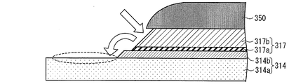
- FIG. 14 is a sectional view of a part of a conventional active matrix substrate.
- FIG. 14 shows only a part near the TFT 325 of the conventional active matrix substrate 300.
- a conventional active matrix substrate 300 includes a glass 311, a scanning wiring 312, an insulating layer 313, a semiconductor layer 314, a signal electrode 316, a drain electrode 317, a protective layer 318, an interlayer insulating layer 319, and a pixel electrode. 320 is provided. These are laminated as shown in FIG. 14 to constitute a TFT 325.
- the semiconductor layer 314 includes a channel layer 314a and an electrode contact layer 314b.
- the signal electrode 316 includes a lower layer signal electrode 316a and an upper layer signal electrode 316b
- the drain electrode 317 includes a lower layer drain electrode 317a and an upper layer drain electrode 317b.
- the upper layer is laminated so as to cover the entire upper surface of the lower layer.
- the material used for the upper drain electrode 317b may diffuse.
- a process in which the material used for the upper drain electrode 317b may be diffused for example, a process of dry-etching the drain electrode 317, a process of forming a material for the protective layer 318 by a CVD method, or the like can be given. If the material diffused in this way moves onto the semiconductor layer 314, the TFT characteristics deteriorate.
- FIG. 13 is a diagram for explaining a conventional method for manufacturing an active matrix substrate, and particularly shows a cross-sectional structure when the drain electrode 317 is patterned.
- the distance between the upper layer drain electrode 317b and the semiconductor layer 314 is short. Therefore, for example, when the material used for the upper drain electrode 317b is diffused by dry etching or the like, the diffused material is likely to move onto the semiconductor layer 314 as indicated by an arrow in FIG.
- the source electrode and the drain electrode are patterned by wet etching, and the barrier pattern is patterned by dry etching so that the source electrode and the drain electrode are etched larger than the barrier pattern (overetching).
- the amount by which the source and drain electrodes are over-etched is not defined at all. Therefore, when the amount of overetching is small, there is a problem that the material used for the source electrode and the drain electrode diffuses and moves onto the semiconductor layer. Further, when the amount of over-etching is large, there arises a problem that the resist is peeled off or it is difficult to form a thin wiring.
- Patent Document 1 neither describes these problems nor a method for solving these problems. For this reason, it is difficult to easily form TFTs having stable characteristics in the conventional wiring structure.
- the present invention has been made in view of the above-described problems of the prior art, and an object of the present invention is to provide an active matrix substrate having a wiring structure capable of easily forming a TFT having stable characteristics, and the same.
- a display panel and a display device having the above are provided.
- an active matrix substrate includes a thin film transistor including a semiconductor layer and an electrode electrically connected to the semiconductor layer.
- the electrode includes a first metal layer laminated so as to cover a part of the upper surface of the semiconductor layer, and a second metal layer laminated on the first metal layer, and the semiconductor layer and the first metal layer.
- the first metal layer and the second metal layer are configured in a stepped manner, and the periphery of the first metal layer and the periphery of the second metal layer are formed in the stepped configuration.
- the distance between and is larger than 0.4 ⁇ m and smaller than 1.5 ⁇ m.
- the semiconductor layer and the second metal are provided by including the first metal layer and the distance between the periphery of the first metal layer and the periphery of the second metal layer is greater than 0.4 ⁇ m.
- the layers can be separated sufficiently. Therefore, in the process of manufacturing the active matrix substrate, for example, when the electrode is patterned, it is possible to prevent the material used for the second metal layer from moving to the semiconductor layer.
- any metal can be used for the second metal layer without deteriorating the characteristics of the TFT.
- the distance between the peripheral edge of the first metal layer and the peripheral edge of the second metal layer is smaller than 1.5 ⁇ m, it is possible to prevent the resist used for patterning the electrode from being peeled off, and with a thin wiring. Even if it exists, it can form easily. Therefore, according to the present invention, an active matrix substrate capable of easily forming a TFT having stable characteristics can be obtained.
- the active matrix substrate according to the present invention includes a thin film transistor including a semiconductor layer and an electrode electrically connected to the semiconductor layer, and the electrode includes the semiconductor layer.
- the second metal layer has a stepped shape, and the upper surface of the first metal layer covers the first metal layer on the upper surface of the semiconductor layer in the stepped portion.
- FIGS. 4A to 4E are views for explaining a method of manufacturing an active matrix substrate in one embodiment of the present invention.
- FIGS. 5A to 5C are views for explaining a method of manufacturing the counter substrate in one embodiment of the present invention.
- FIGS. 6A to 6C are views for explaining a method of manufacturing an active matrix substrate in one embodiment of the present invention.
- FIGS. 7A to 7D are views for explaining a method of manufacturing an active matrix substrate in another embodiment of the present invention.
- FIGS. 8A to 8E are views for explaining a method of manufacturing an active matrix substrate in another embodiment of the present invention.
- FIGS. 9A to 9F are views for explaining a method of manufacturing an active matrix substrate in another embodiment of the present invention.
- FIGS. 10A to 10F are views for explaining a method of manufacturing an active matrix substrate in another embodiment of the present invention. It is a graph which shows the TFT characteristic of the active matrix substrate in one Example of this invention. It is a figure for demonstrating the manufacturing method of the active matrix substrate in one Embodiment of this invention. It is a figure for demonstrating the manufacturing method of the conventional active matrix substrate. A sectional view of a part of a conventional active matrix substrate is shown. (A)-(d) is a figure showing the electron microscope image of the active matrix substrate in the time of completion
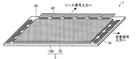
- FIG. 3 is a diagram showing a liquid crystal display device according to an embodiment of the present invention.
- the liquid crystal display device 1 is a liquid crystal display device 1 having an active matrix type liquid crystal display panel (display panel) 2. As shown in FIG. 3, the liquid crystal display panel 2 is formed by laminating an active matrix substrate 10A and a counter substrate 30 with a liquid crystal layer (not shown) interposed therebetween.
- the active matrix substrate 10A has pixel electrodes arranged in a matrix, is provided with a display area that displays an image that is visually recognized by the observer, and an outside of the display area, and the image is not visually recognized by the observer. It is divided into a display area.
- a scanning wiring terminal portion 41 for the scanning wiring 12 to receive an external signal and a signal wiring terminal portion 42 for the signal wiring to receive an external signal are provided in the non-display area.
- the scanning wiring terminal portion 41 and the signal wiring terminal portion 42 are connected to the terminal wiring 43 connected to the scanning wiring 12 or the signal wiring, respectively.
- a plurality of scanning wirings 12 and a plurality of signal wirings are arranged so as to intersect with each other, and a thin film transistor (hereinafter also referred to as “TFT”) 25 is formed in the vicinity of the intersection.
- the TFT 25 constitutes a pixel portion.
- a signal electrode (electrode) 16, a drain electrode (electrode) 17, and a pixel electrode 20 are provided. The structure of the TFT 25 will be described later.
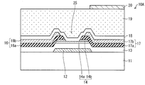
- FIG. 1 shows a cross-sectional view of a part of an active matrix substrate in an embodiment of the present invention.
- FIG. 1 shows only a part of the active matrix substrate 10A near the TFT 25.
- the active matrix substrate 10A includes a glass 11, a scanning wiring 12, an insulating layer 13, a semiconductor layer 14, a signal electrode 16, a drain electrode 17, a protective layer 18, an interlayer insulating layer 19, and a pixel electrode 20. These are laminated as shown in FIG. 1 to constitute the TFT 25.
- the TFT 25 has an inverted stagger type (bottom gate) structure. That is, in the TFT 25, the scanning wiring 12 is disposed in the lowermost layer, the insulating layer 13 and the semiconductor layer 14 are formed on the scanning wiring 12, and the signal electrode 16 and the drain electrode are formed on the insulating layer 13 and the semiconductor layer 14. 17 is formed.
- the semiconductor layer 14 includes a channel layer 14a and an electrode contact layer 14b, and is a layer for conducting the signal electrode 16 and the drain electrode 17.
- amorphous silicon or the like may be used, and an oxide semiconductor such as zinc oxide (ZnO) or an amorphous thin film (IGZO) having a composition of indium oxide-gallium oxide-zinc oxide is used. Also good.
- ZnO zinc oxide
- IGZO amorphous thin film
- the electrode contact layer 14b may be, for example, an N + contact layer doped with an n-type impurity at a high concentration, and for example, N + amorphous silicon may be used.
- the signal electrode 16 is an electrode provided on the signal wiring.
- the signal electrode 16 includes a lower layer signal electrode (first metal layer) 16 a and an upper layer signal electrode (second metal layer) 16 b, and is electrically connected to the semiconductor layer 14.
- the drain electrode 17 includes a lower layer drain electrode (first metal layer) 17 a and an upper layer drain electrode (second metal layer) 17 b and is electrically connected to the semiconductor layer 14.
- the drain electrode 17 is electrically connected to the signal electrode 16 through the semiconductor layer 14.
- the material used for the lower signal electrode 16a and the lower drain electrode 17a is not particularly limited, but it is preferable to use a metal that is difficult to diffuse in the manufacturing process.
- a metal that is difficult to diffuse in the manufacturing process For example, titanium (Ti), tantalum (Ta), molybdenum (Mo), or an alloy thereof can be used. With such a configuration, since the metal used for the lower signal electrode 16a and the lower drain electrode 17a does not diffuse into the semiconductor layer 14 in the manufacturing process, a TFT having good characteristics can be formed.
- the material used for the upper signal electrode 16b and the upper drain electrode 17b is not particularly limited, and examples thereof include copper (Cu), copper alloy, and aluminum (Al), and copper or copper alloy is preferable. Since copper or copper alloy has low resistance, the resistance of the signal electrode 16 or the drain electrode 17 can be reduced.
- copper for example, pure copper can be used.
- copper alloys include copper-magnesium alloys (CuMg), copper-manganese alloys (CuMn), copper-aluminum alloys (CuAl), copper-titanium alloys (CuTi), copper-zirconium alloys (CuZr), copper -A molybdenum alloy (CuMo) or the like can be used.
- the scanning wiring 12 includes a lower layer scanning wiring 12a and an upper layer scanning wiring 12b.
- the material used for the lower layer scanning wiring 12a the same material as that used for the lower layer signal electrode 16a and the lower layer drain electrode 17a can be used.
- the metal used for the upper scanning line 12b the same material as that used for the upper signal electrode 16b and the upper drain electrode 17b can be used.
- the insulating layer for example, silicon nitride (SiNx), silicon dioxide (SiO 2 ), or the like may be used, or SiNx and SiO 2 may be stacked.
- the thickness of the gate insulating film 103 is preferably 1000 to 5000 mm.
- the protective layer 18 for example, silicon nitride (SiNx), silicon dioxide (SiO 2 ) or the like can be used.
- a layer having photosensitivity is preferably used, and for example, a photosensitive acrylic resin or the like can be used.
- a transparent conductive material such as indium tin oxide (ITO) or indium oxide-zinc oxide (IZO) can be used.
- FIG. 2 is a cross-sectional view of the main part of the active matrix substrate in one embodiment of the present invention.
- the signal electrode 16 in the TFT 25 is configured in the same manner as the drain electrode 17.
- the drain electrode 17 can be appropriately replaced with the signal electrode 16
- the lower layer drain electrode 17a can be replaced with the lower layer signal electrode 16a
- the upper layer drain electrode 17b can be replaced with the upper layer signal electrode 16b.
- the lower drain electrode 17 a of the drain electrode 17 is laminated so as to cover a part of the upper surface of the semiconductor layer 14.
- the lower drain electrode 17a is laminated so as to cover a part of the upper surface of the electrode contact layer 14b in the semiconductor layer.
- the upper drain electrode 17b is stacked on the lower drain electrode 17a.
- the channel layer 14 a, the electrode contact layer 14 b, the lower layer drain electrode 17 a, and the upper layer drain electrode 17 b are configured stepwise in the TFT 25.
- the lower drain electrode 17a protrudes from the upper drain electrode 17b in the direction of the portions 14aa and 14ba that are not covered by the lower drain electrode 17a on the upper surface of the semiconductor layer 14.
- a portion 17aa not covered with the upper layer drain electrode 17b is provided.
- the distance A between the periphery of the lower drain electrode 17a and the periphery of the upper drain electrode 17b is greater than 0.4 ⁇ m and less than 1.5 ⁇ m.
- the “periphery of the lower layer drain electrode 17 a” refers to a portion where the upper surface of the lower layer drain electrode 17 a or the end face following it contacts the upper surface of the semiconductor layer 14.
- the “periphery of the upper layer drain electrode 17b” refers to a portion where the upper surface of the upper layer drain electrode 17b or the end surface following the upper surface drain electrode 17b contacts the upper surface of the lower layer drain electrode 17a.
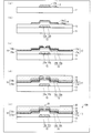
- FIG. 12 is a diagram for explaining a method of manufacturing an active matrix substrate in one embodiment of the present invention, and particularly shows a cross-sectional structure when the drain electrode 17 is patterned.
- the upper drain electrode 17b and the semiconductor layer 14 are sufficiently separated from each other. Therefore, it is possible to prevent the material of the upper drain electrode 17b from moving to the semiconductor layer 14 when the drain electrode 17 is patterned. Therefore, according to the present embodiment, any metal used for the upper drain electrode 17b can be prevented from moving to the semiconductor layer 14 in the manufacturing process. Accordingly, it is possible to prevent deterioration of TFT characteristics and obtain stable characteristics. In other words, in the present embodiment, any metal can be used for the upper drain electrode 17b without degrading the TFT characteristics.
- the distance A is smaller than 1.5 ⁇ m, it is possible to prevent the resist used when patterning the drain electrode 17 from being peeled off, and even a thin wiring can be easily formed. Therefore, with the wiring structure of this embodiment, a TFT having stable characteristics can be easily formed.
- the lower drain electrode 17a may be laminated so as to completely cover the electrode contact layer 14b.
- the lower drain electrode 17a is laminated together with the electrode contact layer 14b so as to cover a part of the upper surface of the channel layer 14a, and the channel layer 14a, the lower drain electrode 17a, and the upper drain electrode 17b are stepped. Configured.
- the electrode contact layer 14b may completely cover the channel layer 14a.
- the lower layer drain electrode 17a is laminated so as to cover a part of the upper surface of the electrode contact layer 14b, and the electrode contact layer 14b, the lower layer drain electrode 17a, and the upper layer drain electrode 17b are formed in a stepped shape.
- the active matrix substrate according to the present embodiment can be suitably used for a display panel in a display device.
- Ti is used for the lower layer scanning wiring 12a, the lower layer signal electrode 16a, and the lower layer drain electrode 17a
- Cu is used as an example for the upper layer scanning wiring 12b, the upper layer signal electrode 16b, and the upper layer drain electrode 17b. I will explain.
- the active matrix substrate 10A in the present embodiment is manufactured by five photolithography processes.
- 4A to 4E are views for explaining a method of manufacturing an active matrix substrate in one embodiment of the present invention, and show a cross-sectional structure at the time when each step is completed. 4A to 4E show only a part near the TFT 25 of the active matrix substrate 10A. Therefore, here, a manufacturing process near the TFT 25 will be described.
- the scanning wiring 12 is formed as shown in FIG. First, Ti is formed as a lower layer scanning line 12a and Cu is formed as an upper layer scanning line 12b successively on the glass 11 by sputtering, and then a resist pattern is formed by photolithography. Thereafter, wet etching is performed by a method to be described later to form patterns of the lower layer scanning wiring 12a and the upper layer scanning wiring 12b, and then the resist is peeled and washed.
- this step although not particularly limited, it is preferable to form a Ti film of 30 to 150 nm and a Cu film of 200 to 500 nm.
- the insulating layer 13, the channel layer 14a, and the electrode contact layer 14b are formed.
- silicon nitride as the insulating layer 13, amorphous silicon as the channel layer 14a, and n + amorphous silicon as the electrode contact layer 14b are successively formed by CVD.
- a resist pattern is formed by photolithography.
- dry etching is performed to form patterns of the channel layer 14a and the electrode contact layer 14b, and then the resist is peeled and washed.
- the signal electrode 16 and the drain electrode 17 are formed as shown in FIG.
- the signal electrode 16 and the drain electrode 17 are simultaneously formed in the same layer and then formed by patterning.
- a resist pattern is formed by photolithography. Thereafter, wet etching is performed by a method described later to form patterns of the lower layer signal electrode 16a, the upper layer signal electrode 16b, the lower layer drain electrode 17a, and the upper layer drain electrode 17b. Further, a part of the electrode contact layer 14b is removed by dry etching. Thereafter, the resist is peeled and washed.
- this step although not particularly limited, it is preferable to form a Ti film of 30 to 150 nm and a Cu film of 100 to 400 nm.
- a protective layer 18 and an interlayer insulating layer 19 are formed.
- silicon nitride is deposited as the protective layer 18 by CVD.
- a pattern is formed by photolithography.
- dry etching is performed to form a pattern of the protective layer 18 and the interlayer insulating layer 19.
- silicon nitride as the protective layer 18 is preferably formed to a thickness of 100 to 700 nm.
- the pixel electrode 20 is formed as shown in FIG. First, after forming a transparent conductive material such as indium tin oxide (ITO) or indium oxide-zinc oxide (IZO) as a film for forming the pixel electrode 20 by sputtering, a resist pattern is formed by photolithography. Thereafter, the pattern of the pixel electrode 20 is formed by wet etching, and then the resist is peeled and washed.
- a transparent conductive material such as indium tin oxide (ITO) or indium oxide-zinc oxide (IZO)
- ITO indium tin oxide
- IZO indium oxide-zinc oxide
- a transparent conductive material as the pixel electrode 20 it is preferable to form a transparent conductive material as the pixel electrode 20 to a thickness of 50 to 200 nm.
- the active matrix substrate 10A is manufactured through the above steps.
- the materials as described above and the thicknesses of the respective layers are not necessarily limited, and materials conventionally used as a material for the active matrix substrate can be used.
- the scanning wiring 12, the signal electrode 16, and the drain electrode 17 in the TFT 25 of the present embodiment have a two-layer structure of a lower layer and an upper layer as shown in FIG. Has been.
- the wet etching in the first step and the third step described above is performed by the method described below.
- FIGS. 6 (a) to 6 (c) are views for explaining a method of manufacturing an active matrix substrate in one embodiment of the present invention, and in particular, cross-sections at each stage when patterning the scanning wiring 12 The figure is shown.
- wet etching is performed by the method described in (1) to (3) below, and the scanning wiring 12 is patterned.
- Ti is formed on the glass 11 as the lower layer scanning wiring 12a and Cu is formed as the upper layer scanning wiring 12b.
- a resist 50 is formed by lithography.
- an etchant having a H 2 O 2 concentration of 5% or more and less than 20% and a fluorine compound concentration of 0.5% or more and less than 3%.
- Cu can be etched faster than Ti.
- the lower-layer scanning wiring 12a and the upper-layer scanning wiring 12b are formed in a step shape by making the Cu shift amount (etching rate) larger than the Ti shift amount. be able to.
- the etchant used in the present embodiment is not particularly limited, but preferably contains H 2 O 2 and a fluorine compound.
- the shift amount of Cu can be adjusted by the concentration of H 2 O 2 contained in the etchant, while the shift amount of Ti can be adjusted by the concentration of the fluorine compound. Therefore, it is preferable to appropriately adjust the concentrations of H 2 O 2 and the fluorine compound contained in the etchant based on the desired shift amounts of Cu and Ti.
- the signal electrode 16 and the drain electrode 17 can be patterned by performing wet etching by the method described in the above (1) to (3).
- the etchant used in the above method (2) has an H 2 O 2 concentration of 5% or more and less than 20% and a fluorine compound concentration of 0.5% or more and less than 3%.
- the etching time is preferably 1.3 to 3 times the just etching time.
- the “just etching time” refers to a time for etching the upper layer (here, Cu) of the signal electrode 16 and the drain electrode 17 with the same width as the width of the resist 50.
- the distance A between the peripheral edge of the lower layer and the peripheral edge of the upper layer in each of the signal electrode 16 and the drain electrode 17 can be made larger than 0.4 ⁇ m and smaller than 1.5 ⁇ m.
- FIGS. 5A to 5C are views for explaining a method of manufacturing the counter substrate in one embodiment of the present invention, and show a cross-sectional structure at the time when each step is completed.
- the counter substrate 30 is manufactured by three photolithography processes described in (1) to (3) below.
- a photosensitive material is used and a black matrix 32 and red, green or blue color filter 33 layers are formed on a glass 31 by photolithography.
- a pixel electrode 34 is deposited by sputtering to a thickness of 50 to 200 nm, and then a pattern is formed by photolithography and wet etching to form a counter electrode. To do.
- a photo spacer 35 is formed by photolithography using a photosensitive material.
- polyimide is formed as an alignment film on the active matrix substrate 10A and the counter substrate 30 by a printing method.
- the liquid crystal display device 1 of the present embodiment in which the active matrix substrate 10A and the counter substrate 30 are arranged so as to overlap each other and a liquid crystal layer is formed therebetween is manufactured.
- the active matrix substrate and the display panel according to one embodiment of the present invention are not limited to the above-described liquid crystal display device, and can be applied to a display device in organic EL, inorganic EL, electrophoresis, and the like. Accordingly, since the active matrix substrate capable of easily forming TFTs having stable characteristics is provided, a high-quality display device can be easily manufactured.
- the signal electrode 16 and the drain electrode 17 are patterned by wet etching and dry etching in the third step in the manufacturing process of the active matrix substrate 10A of the first embodiment. Except for this point, the same method as in the first embodiment is used. Patterning of the scanning wiring 12, the signal electrode 16, and the drain electrode 17 in the present embodiment is performed by the method described below.
- Ti is formed on the glass 11 as the lower layer scanning wiring 12a and Cu is formed as the upper layer scanning wiring 12b.
- a resist 50 is formed by lithography.
- an etchant having a H 2 O 2 concentration of 5% or more and less than 20% and a fluorine compound concentration of 0.5% or more and less than 3%.
- Cu can be etched faster than Ti.
- the lower-layer scanning wiring 12a and the upper-layer scanning wiring 12b are formed in a step shape by making the Cu shift amount (etching rate) larger than the Ti shift amount. be able to.
- the etchant used in the present embodiment is not particularly limited, but preferably contains H 2 O 2 and a fluorine compound.
- the shift amount of Cu can be adjusted by the concentration of H 2 O 2 contained in the etchant, while the shift amount of Ti can be adjusted by the concentration of the fluorine compound. Therefore, it is preferable to appropriately adjust the concentrations of H 2 O 2 and the fluorine compound contained in the etchant based on the desired shift amounts of Cu and Ti.
- FIGS. 7A to 7D are views for explaining a method of manufacturing an active matrix substrate according to another embodiment of the present invention. In particular, each stage at the time of patterning the signal electrode 16 is shown. A cross-sectional view is shown. The signal electrode 16 and the drain electrode 17 are patterned by the method shown here.
- wet etching and dry etching are performed by the method described in (4) to (7) below, and the signal electrode 16 and the drain electrode 17 are patterned.
- Ti is formed as a lower layer signal electrode 16a and Cu is formed as an upper layer signal electrode 16b on the base.
- a resist 50 is formed by photolithography.
- the resist 50 is not etched by wet etching, Cu is etched to be narrower than the width of the resist 50, and in the subsequent dry etching, Ti is etched with the same width as the resist 50. Therefore, the shift amount difference between Cu and Ti can be increased.
- the wet etching time in the present embodiment is not particularly limited, but it is preferable to adjust appropriately based on a desirable shift amount difference between Cu and Ti.
- the lower layer signal electrode 16a and the upper layer signal electrode 16b can be configured in a step shape by making the Cu shift amount larger than the Ti shift amount.
- the etchant and etching time used in the wet etching (5) of the above-described method are such that the distance A between the lower edge and the upper edge of the signal electrode 16 and the drain electrode 17 is 0.4 ⁇ m. It is preferably adjusted so as to be larger and smaller than 1.5 ⁇ m.
- the upper layer is made of copper, it is preferable to perform etching for 2 to 4 times the just etching time using an etchant having a H 2 O 2 concentration of 5% or more and less than 10%.
- the distance A between the peripheral edge of the lower layer and the peripheral edge of the upper layer in the signal electrode 16 and the drain electrode 17 can be made larger than 0.4 ⁇ m and smaller than 1.5 ⁇ m.
- the present embodiment is different from the first embodiment and the second embodiment only in that the active matrix substrate 10B is not provided with the interlayer insulating layer 19, and the other is the same as the first embodiment and the second embodiment. It is configured. Therefore, in this embodiment, only points different from the first embodiment and the second embodiment will be described, and members having the same configuration are denoted by the same member numbers, and description thereof will be omitted.
- FIGS. 8A to 8E are views for explaining a method of manufacturing an active matrix substrate according to another embodiment of the present invention, and show a cross-sectional structure at the time when each step is completed. . Further, FIGS. 8A to 8E show only a part near the TFT 25 of the active matrix substrate 10A. Therefore, here, a manufacturing process near the TFT 25 will be described.
- the scanning wiring 12 is formed as shown in FIG. 8A by using the same method as the first step in the first and second embodiments.
- the protective layer 18 is formed as shown in FIG. First, after a silicon nitride film is formed as the protective layer 18 by the CVD method, a resist pattern is formed by photolithography. After the pattern of the protective layer 18 is formed by dry etching, the resist is peeled and washed.
- silicon nitride as the protective layer 18 is preferably formed to a thickness of 100 to 700 nm.
- the pixel electrode 20 is formed as shown in FIG. 8E by using the same method as the fifth step in the first and second embodiments.
- the active matrix substrate 10B is manufactured through the above steps.
- the present embodiment is different from the first embodiment and the second embodiment in that the channel protective layer 21 is provided on the active matrix substrate 10C, and the rest is the same as the first embodiment and the second embodiment. It is configured. Therefore, in the present embodiment, only differences from the first embodiment and the second embodiment will be described, and members having the same configuration are denoted by the same member numbers, and description thereof is omitted.
- FIGS. 9A to 9F are views for explaining a method of manufacturing an active matrix substrate in another embodiment of the present invention, and show a cross-sectional structure at the time when each step is completed. . Further, FIGS. 9A to 9F show only a part near the TFT 25 of the active matrix substrate 10C. Therefore, here, a manufacturing process near the TFT 25 will be described.
- the scanning line 12 is formed as shown in FIG. 9A by using the same method as the first step in the first and second embodiments.
- the insulating layer 13, the channel layer 14a, and the channel protective layer 21 are formed.
- silicon nitride is continuously formed as the insulating layer 13
- amorphous silicon is used as the channel layer 14 a
- silicon nitride is used as the channel protective layer 21 by CVD.
- a resist pattern is formed by photolithography, dry etching is performed, and the pattern of the channel protective layer 21 is formed. Then, the resist is peeled and washed.
- the electrode contact layer 14b, the signal electrode 16, and the drain electrode 17 are formed.
- the signal electrode 16 and the drain electrode 17 are simultaneously formed in the same layer and then formed by patterning.
- n + amorphous silicon is deposited as the electrode contact layer 14b by the CVD method.
- Ti is successively formed as the lower layer signal electrode 16a and the lower layer drain electrode 17a by sputtering, and Cu is continuously formed as the upper layer signal electrode 16b and the upper layer drain electrode 17b.
- a resist pattern is formed by photolithography. Thereafter, the patterns of the lower layer signal electrode 16a, the upper layer signal electrode 16b, the lower layer drain electrode 17a, and the upper layer drain electrode 17b are formed by the method described in the first embodiment or the second embodiment. Further, a part of the electrode contact layer 14b on the channel protective layer 21 is removed by dry etching. Thereafter, the resist is peeled and washed.
- n + amorphous silicon of 50 to 150 nm, Ti of 30 to 150 nm, and Cu of 100 to 400 nm as the electrode contact layer 14b.
- the protective layer 18 and the interlayer insulating layer 19 are used as shown in FIG. 9E by using the same method as the fourth step in the first and second embodiments. Form.
- the pixel electrode 20 is formed as shown in FIG. 9F by using the same method as the fifth step in the first embodiment and the second embodiment.
- the active matrix substrate 10C is manufactured through the above steps.
- the black matrix 22 and the color filter 23 are formed between the protective layer 18 and the interlayer insulating layer 19 in the active matrix substrate 10D, and the black matrix 32 and the color filter are formed on the counter substrate.
- the point that the layer of the filter 33 is not formed is different from the first embodiment and the second embodiment, and the rest is configured in the same manner as the first embodiment and the second embodiment. Therefore, in the present embodiment, only differences from the first embodiment and the second embodiment will be described, and members having the same configuration are denoted by the same member numbers, and description thereof is omitted.
- FIGS. 10A to 10F are views for explaining an active matrix substrate manufacturing method according to another embodiment of the present invention, showing a cross-sectional structure at the time when each step is completed. . Further, FIGS. 10A to 10F show only a part near the TFT 25 of the active matrix substrate 10D. Therefore, here, a manufacturing process near the TFT 25 will be described.
- the first step, (2) the second step, and (3) the third step are the same as those in the first embodiment and the second embodiment, and are omitted here.
- the cross-sectional structures at the time when these steps are completed are shown in FIGS. 10 (a) to 10 (c).
- the protective layer 18, the black matrix 22, and the color filter 23 are formed.
- silicon nitride is deposited as the protective layer 18 by CVD.
- a black matrix 22 and red, green, and blue color filter 23 layers are formed by photolithography using a photosensitive material.
- silicon nitride as the protective layer 18 is preferably formed to a thickness of 100 to 700 nm.
- an interlayer insulating layer 19 is formed as shown in FIG. After forming a photosensitive interlayer insulating film material as the interlayer insulating layer 19, a pattern is formed by photolithography. Thereafter, dry etching is performed to form a pattern of the interlayer insulating layer 19.
- the pixel electrode 20 is formed as shown in FIG. First, after forming a transparent conductive material such as ITO (or IZO) as a film for forming the pixel electrode 20 by sputtering, a resist pattern is formed by photolithography. Thereafter, the pattern of the pixel electrode 20 is formed by wet etching, and then the resist is peeled and washed.
- a transparent conductive material such as ITO (or IZO)
- a transparent conductive material as the pixel electrode 20 it is preferable to form a transparent conductive material as the pixel electrode 20 to a thickness of 50 to 200 nm.
- the active matrix substrate 10D is manufactured through the above steps.
- the counter substrate since the active matrix substrate 10D includes the black matrix 22 and the color filter 23, the counter substrate does not need to include the black matrix and color filter layers. Therefore, although not shown, the counter substrate of the present embodiment is configured not to include a black matrix and a color filter.
- Example 1 An active matrix substrate having a TFT having the same structure as that shown in FIG. 1 was manufactured, and TFT characteristics were measured.
- the active matrix substrate was manufactured using the method described in the second embodiment. That is, in the third step, patterning of the signal electrode 16 and the drain electrode 17 was performed by wet etching and dry etching.
- wet etching was performed under three kinds of conditions to produce three kinds of active matrix substrates.
- the three types of conditions were that an etchant with an appropriate H 2 O 2 concentration was used, and the wet etching time was 1.5 times, 1.75 times, and 2 times the just etching time, respectively.
- TFTs having distances A between the lower edge of the signal electrode 16 and the drain electrode 17 and the upper edge of the upper layer of 0.2 ⁇ m, 0.3 ⁇ m, and 0.45 ⁇ m were formed.
- the TFT characteristics were investigated using these active matrix substrates.
- the TFT characteristics were measured using a manual prober and a semiconductor parameter analyzer (manufactured by Agilent).
- FIG. 11 is a graph showing TFT characteristics of an active matrix substrate in one example of the present invention.
- the distance A is 0.5 ⁇ m or less, that is, 0.2 ⁇ m or 0.3 ⁇ m
- the TFT characteristics are greatly shifted to the plus side.
- the distance A was 0.45 ⁇ m, good TFT characteristics were obtained.
- Example 2 An active matrix substrate having a TFT having a structure similar to that shown in FIG. 1 was manufactured, and the manufacturing conditions were evaluated.
- the active matrix substrate was manufactured using the method described in the first embodiment. That is, in the third step, patterning of the signal electrode 16 and the drain electrode 17 was performed only by wet etching.
- wet etching was performed under three types of conditions to produce three types of active matrix substrates.
- the three types of conditions are to produce three types of etchants in which the H 2 O 2 concentration in the etchant is set in three stages, and to perform etching using each etchant.
- TFTs having distances A of 1.0 ⁇ m, 1.3 ⁇ m, and 1.6 ⁇ m, respectively, between the lower edge and the upper edge of the signal electrode 16 and the drain electrode 17 were formed.
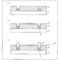
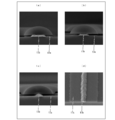
- 15A to 15D are views showing electron microscope images of the active matrix substrate at the end of the wet etching in the third step.
- 15A is a cross section of an active matrix substrate having a distance A of 1.0 ⁇ m
- FIG. 15B is a cross section of an active matrix substrate having a distance A of 1.3 ⁇ m
- FIG. 15C Indicates a cross section of an active matrix substrate having a distance A of 1.6 ⁇ m.
- FIG. 15D is a top view of the active matrix substrate shown in FIG. 15C with the resist 50 removed.
- the resist 50 remained stably.
- This active matrix substrate could be dry etched after wet etching.
- This example shows that when the distance A is 1.0 ⁇ m or 1.3 ⁇ m, the resist 50 used for patterning the drain electrode 17 can be prevented from peeling off. In other words, it was strongly suggested that when the distance A is smaller than 1.5 ⁇ m, the resist can be prevented from being peeled off, and even a thin wiring can be easily formed.
- the second metal layer preferably contains copper or a copper alloy.
- the resistance of an electrode can be made low. Further, when the active matrix substrate is manufactured, the copper or copper alloy can be prevented from moving to the semiconductor layer, so that the TFT characteristics can be prevented from being deteriorated and stable characteristics can be obtained.
- the first metal layer includes at least one selected from the group consisting of titanium, tantalum, molybdenum, and alloys thereof.
- titanium, tantalum, molybdenum, and alloys thereof are not easily diffused by dry etching or the like, and thus do not move onto the semiconductor layer in the manufacturing process. Accordingly, it is possible to prevent deterioration of TFT characteristics and obtain stable characteristics.
- the electrode is preferably a signal electrode or a drain electrode.
- any metal can be used for the second metal layer of the signal electrode or the drain electrode without deteriorating the characteristics of the TFT. Further, the resist used when patterning the signal electrode or the drain electrode can be prevented from being peeled off, and can be easily formed even when the signal electrode or the drain electrode is thin.
- the thin film transistor includes the two electrodes, and a portion of the upper surface of the semiconductor layer that is not covered with the first metal layer is interposed between the thin film transistors. It is preferable that the stepped portions of each of the electrodes are arranged to face each other.
- one of the two electrodes is a signal electrode and the other is a drain electrode.
- any metal can be used for the second metal layer of the signal electrode and the drain electrode without degrading the characteristics of the TFT. Further, the resist used for patterning the signal electrode and the drain electrode can be prevented from being peeled off, and can be easily formed even when the signal electrode and the drain electrode are thin.
- a display panel according to one embodiment of the present invention includes any one of the active matrix substrates described above.
- a display device according to one embodiment of the present invention includes the above display panel.
- the present invention since it is possible to easily form TFTs having stable characteristics, the present invention can be suitably used when manufacturing high-quality active matrix substrates and liquid crystal display devices.
- Liquid crystal display device 2 Liquid crystal display panel (display panel) 10A active matrix substrate 14 semiconductor layer 16 signal electrode (electrode) 16a Lower layer signal electrode (first metal layer) 16b Upper signal electrode (second metal layer) 17 Drain electrode (electrode) 17a Lower drain electrode (first metal layer) 17b Upper drain electrode (second metal layer) 25 TFT (Thin Film Transistor)
Landscapes
- Physics & Mathematics (AREA)
- Nonlinear Science (AREA)
- Engineering & Computer Science (AREA)
- Microelectronics & Electronic Packaging (AREA)
- Mathematical Physics (AREA)
- Chemical & Material Sciences (AREA)
- Crystallography & Structural Chemistry (AREA)
- General Physics & Mathematics (AREA)
- Optics & Photonics (AREA)
- Thin Film Transistor (AREA)
- Liquid Crystal (AREA)
- Electrodes Of Semiconductors (AREA)
Abstract
Priority Applications (5)
| Application Number | Priority Date | Filing Date | Title |
|---|---|---|---|
| JP2012556833A JP5315468B2 (ja) | 2011-02-07 | 2012-01-31 | アクティブマトリクス基板の製造方法、表示パネル、及び表示装置 |
| KR1020137020500A KR101486180B1 (ko) | 2011-02-07 | 2012-01-31 | 액티브 매트릭스 기판의 제조 방법, 표시 패널 및 표시 장치 |
| EP12745003.9A EP2674981A4 (fr) | 2011-02-07 | 2012-01-31 | Substrat à matrice active, panneau d'affichage et dispositif d'affichage |
| US13/983,655 US9070600B2 (en) | 2011-02-07 | 2012-01-31 | Active matrix substrate, display panel, and display device |
| CN201280007738.XA CN103348484B (zh) | 2011-02-07 | 2012-01-31 | 有源矩阵基板、显示面板和显示装置 |
Applications Claiming Priority (2)
| Application Number | Priority Date | Filing Date | Title |
|---|---|---|---|
| JP2011024299 | 2011-02-07 | ||
| JP2011-024299 | 2011-02-07 |
Publications (1)
| Publication Number | Publication Date |
|---|---|
| WO2012108301A1 true WO2012108301A1 (fr) | 2012-08-16 |
Family
ID=46638517
Family Applications (1)
| Application Number | Title | Priority Date | Filing Date |
|---|---|---|---|
| PCT/JP2012/052107 Ceased WO2012108301A1 (fr) | 2011-02-07 | 2012-01-31 | Substrat à matrice active, panneau d'affichage et dispositif d'affichage |
Country Status (7)
| Country | Link |
|---|---|
| US (1) | US9070600B2 (fr) |
| EP (1) | EP2674981A4 (fr) |
| JP (1) | JP5315468B2 (fr) |
| KR (1) | KR101486180B1 (fr) |
| CN (1) | CN103348484B (fr) |
| TW (1) | TWI507800B (fr) |
| WO (1) | WO2012108301A1 (fr) |
Cited By (4)
| Publication number | Priority date | Publication date | Assignee | Title |
|---|---|---|---|---|
| JP2014099595A (ja) * | 2012-10-17 | 2014-05-29 | Semiconductor Energy Lab Co Ltd | 半導体装置 |
| JP2018139325A (ja) * | 2013-03-28 | 2018-09-06 | 株式会社半導体エネルギー研究所 | 半導体装置 |
| US10164118B2 (en) | 2014-11-28 | 2018-12-25 | Sharp Kabushiki Kaisha | Semiconductor device and method for producing same |
| JP2019024124A (ja) * | 2013-06-21 | 2019-02-14 | 株式会社半導体エネルギー研究所 | 半導体装置 |
Families Citing this family (10)
| Publication number | Priority date | Publication date | Assignee | Title |
|---|---|---|---|---|
| CN103295970B (zh) * | 2013-06-05 | 2015-04-29 | 京东方科技集团股份有限公司 | 阵列基板、其制造方法及显示装置 |
| KR101527117B1 (ko) * | 2013-06-27 | 2015-06-09 | 삼성디스플레이 주식회사 | 식각액 조성물, 이를 이용한 금속 배선 제조 방법 및 박막 트랜지스터 기판 제조방법 |
| CN104319285A (zh) * | 2014-10-27 | 2015-01-28 | 京东方科技集团股份有限公司 | 一种薄膜晶体管及其制备方法、阵列基板 |
| TWI585954B (zh) * | 2016-03-02 | 2017-06-01 | 群創光電股份有限公司 | 電晶體陣列基板及應用之顯示面板 |
| KR102068870B1 (ko) | 2016-06-17 | 2020-01-21 | 주식회사 엘지화학 | 전극 구조체, 이를 포함하는 전자 소자 및 이의 제조방법 |
| CN107039284A (zh) * | 2017-04-17 | 2017-08-11 | 武汉华星光电技术有限公司 | 一种制作低温多晶硅薄膜晶体管的方法 |
| US10651257B2 (en) * | 2017-12-18 | 2020-05-12 | Wuhan China Star Optoelectronics Semiconductor Display Technology Co., Ltd. | Array substrate and manufacturing method thereof |
| KR20210062478A (ko) | 2019-11-21 | 2021-05-31 | 대한민국(전북기계공업고등학교장) | 음성인식 자외선 섬유 살균탈취기 |
| US12238957B2 (en) | 2020-08-04 | 2025-02-25 | Samsung Display Co., Ltd. | Display apparatus |
| CN112599630B (zh) * | 2020-12-07 | 2022-06-10 | Tcl华星光电技术有限公司 | 光传感器和显示装置 |
Citations (3)
| Publication number | Priority date | Publication date | Assignee | Title |
|---|---|---|---|---|
| JP2006261705A (ja) * | 2006-06-23 | 2006-09-28 | Sharp Corp | 薄膜トランジスタ及びその製造方法 |
| JP2008166789A (ja) | 2006-12-26 | 2008-07-17 | Lg Display Co Ltd | 液晶表示装置用アレイ基板及びその製造方法 |
| JP2009071285A (ja) * | 2007-08-17 | 2009-04-02 | Semiconductor Energy Lab Co Ltd | 表示装置の作製方法 |
Family Cites Families (8)
| Publication number | Priority date | Publication date | Assignee | Title |
|---|---|---|---|---|
| JP2590938B2 (ja) | 1987-10-02 | 1997-03-19 | 旭硝子株式会社 | 薄膜トランジスタ基板 |
| US5539219A (en) * | 1995-05-19 | 1996-07-23 | Ois Optical Imaging Systems, Inc. | Thin film transistor with reduced channel length for liquid crystal displays |
| JP2000101091A (ja) * | 1998-09-28 | 2000-04-07 | Sharp Corp | 薄膜トランジスタ |
| KR100799464B1 (ko) * | 2001-03-21 | 2008-02-01 | 엘지.필립스 엘시디 주식회사 | 액정표시장치 및 그 제조방법 |
| JP2002341373A (ja) | 2001-05-17 | 2002-11-27 | Matsushita Electric Ind Co Ltd | アクティブマトリクス基板 |
| EP3614442A3 (fr) | 2005-09-29 | 2020-03-25 | Semiconductor Energy Laboratory Co., Ltd. | Dispositif de semiconducteur disposant d'une couche de semiconducteur d'oxyde et son procédé de fabrication |
| US9024311B2 (en) | 2009-06-24 | 2015-05-05 | Sharp Kabushiki Kaisha | Thin film transistor, method for manufacturing same, active matrix substrate, display panel and display device |
| TWI596741B (zh) * | 2009-08-07 | 2017-08-21 | 半導體能源研究所股份有限公司 | 半導體裝置和其製造方法 |
-
2012
- 2012-01-31 US US13/983,655 patent/US9070600B2/en not_active Expired - Fee Related
- 2012-01-31 KR KR1020137020500A patent/KR101486180B1/ko not_active Expired - Fee Related
- 2012-01-31 JP JP2012556833A patent/JP5315468B2/ja not_active Expired - Fee Related
- 2012-01-31 EP EP12745003.9A patent/EP2674981A4/fr not_active Withdrawn
- 2012-01-31 CN CN201280007738.XA patent/CN103348484B/zh not_active Expired - Fee Related
- 2012-01-31 WO PCT/JP2012/052107 patent/WO2012108301A1/fr not_active Ceased
- 2012-02-06 TW TW101103799A patent/TWI507800B/zh not_active IP Right Cessation
Patent Citations (3)
| Publication number | Priority date | Publication date | Assignee | Title |
|---|---|---|---|---|
| JP2006261705A (ja) * | 2006-06-23 | 2006-09-28 | Sharp Corp | 薄膜トランジスタ及びその製造方法 |
| JP2008166789A (ja) | 2006-12-26 | 2008-07-17 | Lg Display Co Ltd | 液晶表示装置用アレイ基板及びその製造方法 |
| JP2009071285A (ja) * | 2007-08-17 | 2009-04-02 | Semiconductor Energy Lab Co Ltd | 表示装置の作製方法 |
Non-Patent Citations (1)
| Title |
|---|
| See also references of EP2674981A4 |
Cited By (13)
| Publication number | Priority date | Publication date | Assignee | Title |
|---|---|---|---|---|
| JP2014099595A (ja) * | 2012-10-17 | 2014-05-29 | Semiconductor Energy Lab Co Ltd | 半導体装置 |
| US11024742B2 (en) | 2013-03-28 | 2021-06-01 | Semiconductor Energy Laboratory Co., Ltd. | Semiconductor device and manufacturing method thereof |
| JP2018139325A (ja) * | 2013-03-28 | 2018-09-06 | 株式会社半導体エネルギー研究所 | 半導体装置 |
| US11990551B2 (en) | 2013-03-28 | 2024-05-21 | Semiconductor Energy Laboratory Co., Ltd. | Semiconductor device and manufacturing method thereof |
| US10566455B2 (en) | 2013-03-28 | 2020-02-18 | Semiconductor Energy Laboratory Co., Ltd. | Semiconductor device and manufacturing method thereof |
| JP2019024124A (ja) * | 2013-06-21 | 2019-02-14 | 株式会社半導体エネルギー研究所 | 半導体装置 |
| JP2021061424A (ja) * | 2013-06-21 | 2021-04-15 | 株式会社半導体エネルギー研究所 | 半導体装置 |
| JP7019791B2 (ja) | 2013-06-21 | 2022-02-15 | 株式会社半導体エネルギー研究所 | 半導体装置 |
| JP2022058842A (ja) * | 2013-06-21 | 2022-04-12 | 株式会社半導体エネルギー研究所 | 半導体装置 |
| JP7241942B2 (ja) | 2013-06-21 | 2023-03-17 | 株式会社半導体エネルギー研究所 | 半導体装置 |
| JP2024026715A (ja) * | 2013-06-21 | 2024-02-28 | 株式会社半導体エネルギー研究所 | 半導体装置 |
| JP7646890B2 (ja) | 2013-06-21 | 2025-03-17 | 株式会社半導体エネルギー研究所 | 半導体装置 |
| US10164118B2 (en) | 2014-11-28 | 2018-12-25 | Sharp Kabushiki Kaisha | Semiconductor device and method for producing same |
Also Published As
| Publication number | Publication date |
|---|---|
| JP5315468B2 (ja) | 2013-10-16 |
| EP2674981A4 (fr) | 2017-08-30 |
| KR101486180B1 (ko) | 2015-01-23 |
| TWI507800B (zh) | 2015-11-11 |
| US20140014952A1 (en) | 2014-01-16 |
| TW201248280A (en) | 2012-12-01 |
| KR20130106877A (ko) | 2013-09-30 |
| US9070600B2 (en) | 2015-06-30 |
| JPWO2012108301A1 (ja) | 2014-07-03 |
| CN103348484B (zh) | 2016-03-30 |
| CN103348484A (zh) | 2013-10-09 |
| EP2674981A1 (fr) | 2013-12-18 |
Similar Documents
| Publication | Publication Date | Title |
|---|---|---|
| JP5315468B2 (ja) | アクティブマトリクス基板の製造方法、表示パネル、及び表示装置 | |
| JP5275519B2 (ja) | 表示装置用基板及びその製造方法、表示装置 | |
| KR101294237B1 (ko) | 프린지 필드 스위칭 모드 액정표시장치용 어레이 기판 및 이의 제조방법 | |
| KR101019048B1 (ko) | 어레이 기판 및 이의 제조방법 | |
| KR101106562B1 (ko) | 어레이 기판 및 이의 제조방법 | |
| CN103915451B (zh) | 一种阵列基板及其制造方法、显示装置 | |
| WO2010150446A1 (fr) | Transistor à couche mince, son procédé de fabrication, substrat à matrice active, panneau d'affichage et dispositif d'affichage | |
| US9159867B2 (en) | Array substrate, manufacturing method thereof, and display device | |
| KR20100005457A (ko) | 박막 트랜지스터 표시판 및 이의 제조 방법 | |
| JP6501514B2 (ja) | 薄膜トランジスタ基板およびその製造方法 | |
| KR20110113040A (ko) | 어레이 기판 | |
| JP2006338008A (ja) | 開口率が向上したアレイ基板、その製造方法及びそれを含む表示装置。 | |
| JP2011077116A (ja) | 配線構造およびそれを備えた表示装置 | |
| JP6196387B2 (ja) | アクティブマトリクス基板 | |
| WO2012169388A1 (fr) | Substrat tft et son procédé de fabrication | |
| JP2010128323A (ja) | アクティブマトリクス基板及び液晶表示装置 | |
| JP2006210477A (ja) | 薄膜トランジスタ及びその製造方法並びに薄膜トランジスタ基板及びその製造方法並びに該薄膜トランジスタを用いた液晶表示装置及び有機el表示装置並びに透明導電積層基板 | |
| KR102084397B1 (ko) | 액정표시장치의 제조방법 | |
| KR20100055127A (ko) | 어레이 기판의 제조방법 | |
| JP2008242086A (ja) | 電気光学装置製造方法 | |
| KR20100055128A (ko) | 어레이 기판의 제조방법 | |
| KR20120003061A (ko) | 어레이 기판 및 이의 제조방법 | |
| KR20110137967A (ko) | 어레이 기판 및 이의 제조방법 | |
| KR20120002785A (ko) | 어레이 기판 및 이의 제조방법 | |
| JP2008268831A (ja) | 電気光学装置及び電気光学装置製造方法 |
Legal Events
| Date | Code | Title | Description |
|---|---|---|---|
| WWE | Wipo information: entry into national phase |
Ref document number: 201280007738.X Country of ref document: CN |
|
| 121 | Ep: the epo has been informed by wipo that ep was designated in this application |
Ref document number: 12745003 Country of ref document: EP Kind code of ref document: A1 |
|
| WWE | Wipo information: entry into national phase |
Ref document number: 2012556833 Country of ref document: JP |
|
| ENP | Entry into the national phase |
Ref document number: 20137020500 Country of ref document: KR Kind code of ref document: A |
|
| NENP | Non-entry into the national phase |
Ref country code: DE |
|
| WWE | Wipo information: entry into national phase |
Ref document number: 2012745003 Country of ref document: EP |
|
| WWE | Wipo information: entry into national phase |
Ref document number: 13983655 Country of ref document: US |