WO2012108363A1 - Creuset, appareil et procédé de dépôt en phase vapeur et procédé de fabrication d'un dispositif d'affichage électroluminescent organique - Google Patents
Creuset, appareil et procédé de dépôt en phase vapeur et procédé de fabrication d'un dispositif d'affichage électroluminescent organique Download PDFInfo
- Publication number
- WO2012108363A1 WO2012108363A1 PCT/JP2012/052549 JP2012052549W WO2012108363A1 WO 2012108363 A1 WO2012108363 A1 WO 2012108363A1 JP 2012052549 W JP2012052549 W JP 2012052549W WO 2012108363 A1 WO2012108363 A1 WO 2012108363A1
- Authority
- WO
- WIPO (PCT)
- Prior art keywords
- vapor deposition
- injection
- film formation
- particles
- substrate
- Prior art date
- Legal status (The legal status is an assumption and is not a legal conclusion. Google has not performed a legal analysis and makes no representation as to the accuracy of the status listed.)
- Ceased
Links
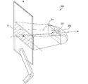
Images


Classifications
-
- C—CHEMISTRY; METALLURGY
- C23—COATING METALLIC MATERIAL; COATING MATERIAL WITH METALLIC MATERIAL; CHEMICAL SURFACE TREATMENT; DIFFUSION TREATMENT OF METALLIC MATERIAL; COATING BY VACUUM EVAPORATION, BY SPUTTERING, BY ION IMPLANTATION OR BY CHEMICAL VAPOUR DEPOSITION, IN GENERAL; INHIBITING CORROSION OF METALLIC MATERIAL OR INCRUSTATION IN GENERAL
- C23C—COATING METALLIC MATERIAL; COATING MATERIAL WITH METALLIC MATERIAL; SURFACE TREATMENT OF METALLIC MATERIAL BY DIFFUSION INTO THE SURFACE, BY CHEMICAL CONVERSION OR SUBSTITUTION; COATING BY VACUUM EVAPORATION, BY SPUTTERING, BY ION IMPLANTATION OR BY CHEMICAL VAPOUR DEPOSITION, IN GENERAL
- C23C14/00—Coating by vacuum evaporation, by sputtering or by ion implantation of the coating forming material
- C23C14/06—Coating by vacuum evaporation, by sputtering or by ion implantation of the coating forming material characterised by the coating material
- C23C14/12—Organic material
-
- C—CHEMISTRY; METALLURGY
- C23—COATING METALLIC MATERIAL; COATING MATERIAL WITH METALLIC MATERIAL; CHEMICAL SURFACE TREATMENT; DIFFUSION TREATMENT OF METALLIC MATERIAL; COATING BY VACUUM EVAPORATION, BY SPUTTERING, BY ION IMPLANTATION OR BY CHEMICAL VAPOUR DEPOSITION, IN GENERAL; INHIBITING CORROSION OF METALLIC MATERIAL OR INCRUSTATION IN GENERAL
- C23C—COATING METALLIC MATERIAL; COATING MATERIAL WITH METALLIC MATERIAL; SURFACE TREATMENT OF METALLIC MATERIAL BY DIFFUSION INTO THE SURFACE, BY CHEMICAL CONVERSION OR SUBSTITUTION; COATING BY VACUUM EVAPORATION, BY SPUTTERING, BY ION IMPLANTATION OR BY CHEMICAL VAPOUR DEPOSITION, IN GENERAL
- C23C14/00—Coating by vacuum evaporation, by sputtering or by ion implantation of the coating forming material
- C23C14/22—Coating by vacuum evaporation, by sputtering or by ion implantation of the coating forming material characterised by the process of coating
- C23C14/24—Vacuum evaporation
-
- H—ELECTRICITY
- H10—SEMICONDUCTOR DEVICES; ELECTRIC SOLID-STATE DEVICES NOT OTHERWISE PROVIDED FOR
- H10K—ORGANIC ELECTRIC SOLID-STATE DEVICES
- H10K71/00—Manufacture or treatment specially adapted for the organic devices covered by this subclass
- H10K71/10—Deposition of organic active material
- H10K71/16—Deposition of organic active material using physical vapour deposition [PVD], e.g. vacuum deposition or sputtering
- H10K71/164—Deposition of organic active material using physical vapour deposition [PVD], e.g. vacuum deposition or sputtering using vacuum deposition
Definitions
- the present invention relates to a vapor deposition technique for forming a pattern of vapor deposition particles on a film formation substrate.
- flat panel displays have been used in various products and fields, and further flat panel displays are required to have larger sizes, higher image quality, and lower power consumption.
- an organic EL display device including an organic EL element using electroluminescence (hereinafter referred to as “EL”) of an organic material is an all-solid-state type, low voltage driving, high speed response, As a flat panel display excellent in terms of self-luminous property and the like, it is attracting a great deal of attention.
- the organic EL display device has, for example, a configuration in which an organic EL element connected to a TFT is provided on a substrate made of a glass substrate or the like provided with a TFT (thin film transistor).
- the organic EL element is a light emitting element that can emit light with high luminance by low-voltage direct current drive, and has a structure in which a first electrode, an organic EL layer, and a second electrode are stacked in this order. Of these, the first electrode is connected to the TFT. In addition, between the first electrode and the second electrode, as the organic EL layer, a hole injection layer, a hole transport layer, an electron blocking layer, a light emitting layer, a hole blocking layer, an electron transport layer, an electron injection layer The organic layer which laminated
- organic EL elements including light emitting layers of red (R), green (G), and blue (B) are arranged and formed on a substrate as sub-pixels. A color image is displayed by selectively emitting light from these organic EL elements with a desired luminance using TFTs.
- an organic EL display device In order to manufacture an organic EL display device, it is necessary to form a light emitting layer made of an organic light emitting material that emits light of each color in a predetermined pattern for each organic EL element. In addition, for a layer that does not require pattern formation for each organic EL element, a thin film is collectively formed on the entire pixel region constituted by the organic EL element.
- a vacuum deposition method for example, a vacuum deposition method, an ink jet method, and a laser transfer method are known.
- a vacuum deposition method is often used.
- a mask also referred to as a deposition mask in which openings having a predetermined pattern are formed is used.
- the deposition surface of the substrate to which the mask is closely fixed is opposed to the deposition source.
- vapor deposition particles film forming material from the vapor deposition source are vapor deposited on the vapor deposition surface through the opening of the mask, thereby forming a thin film having a predetermined pattern.
- Vapor deposition is performed for each color of the light emitting layer (this is called “separate vapor deposition”).
- the evaporation source 201 of the evaporation material and the evaporation material Va which is installed on the opposite side of the evaporation source 201 from the evaporation region R where the evaporation material Va is to be deposited are reflected.
- the vapor deposition apparatus 200 provided with the reflecting member 202 to perform is disclosed.
- the reflecting member 202 of Patent Document 1 is configured such that the cross section has a concave curve and extends in a direction perpendicular to the cross section, and the evaporation source 201 is disposed near the focal point of the curve. ing.
- Japanese Patent Publication Japanese Patent Laid-Open No. 2008-138261 (published on June 19, 2008)
- the entire member constituting the evaporation source 201 (hereinafter referred to as a vapor deposition source component member) is installed in the flow area of the reflected evaporation substance. For this reason, the vapor deposition flow is disturbed by the vapor deposition source component member, and the film thickness distribution of the vapor deposition film on the target surface on which the vapor deposition film is formed is not uniform, or the rate at which the vapor deposition material is deposited on the vapor deposition film formation target surface is reduced. It can be considered that this problem occurs.
- the present invention has been made in view of the above-described problems, and provides a crucible, a vapor deposition apparatus, a vapor deposition method, and a method for manufacturing an organic electroluminescence display device that can prevent a decrease in the vapor deposition rate as much as possible. With the goal.
- a crucible according to the present invention comprises a vapor deposition particle injection member provided with an injection port for injecting vapor deposition particles for forming a vapor deposition film on a deposition film formation target surface of a deposition target substrate, A reflective surface having a concave curved shape that reflects the vapor deposition particles emitted from the injection port toward the vapor deposition film formation target surface, and at least a part of the vapor deposition particle injection member forms the reflection surface and the vapor deposition film. It is installed so that it may be located in the exterior of the flow area of the vapor deposition particle between target surfaces.
- the vapor deposition method according to the present invention is a vapor deposition method for forming a vapor deposition film on a vapor deposition film formation target surface of a deposition target substrate, and an injection step of injecting vapor deposition particles from an injection port of a vapor deposition particle injection member;
- the vapor deposition particle injection member is installed so that at least a part thereof is located outside the flow area of the vapor deposition particles between the reflective surface and the vapor deposition film formation target surface. It is possible to prevent as much as possible a situation in which the flow of vapor deposition particles (hereinafter referred to as vapor deposition flow) is disturbed by the injection member and the film thickness of the vapor deposition film on the vapor deposition film formation target surface is not uniform.
- the organic electroluminescence display device manufacturing method includes a TFT substrate / first electrode manufacturing step of forming a first electrode on a TFT substrate, and an organic layer including an organic layer including at least a light-emitting layer on the TFT substrate.
- An organic electroluminescence display device comprising: a layer vapor deposition step; a second electrode vapor deposition step of vapor depositing a second electrode; and a sealing step of sealing an organic electroluminescence element including the organic layer and the second electrode with a sealing member
- the method of manufacturing, wherein at least one of the organic layer deposition step, the second electrode deposition step, and the sealing step includes each step of any one of the deposition methods. It is.
- the film thickness distribution is made uniform while obtaining a constant deposition rate, an organic electroluminescence display device with little display unevenness can be realized.
- the crucible according to the present invention includes a vapor deposition particle injection member provided with an injection port for injecting vapor deposition particles for forming a vapor deposition film on a surface on which a vapor deposition film is to be formed, and vapor deposition particles injected from the injection port And a concavely curved reflecting surface that reflects toward the surface on which the vapor deposition film is to be formed, and at least part of the vapor deposition particle injection member is vapor deposition particles between the reflection surface and the surface on which the vapor deposition film is to be formed. It is installed outside the basin.
- the vapor deposition method according to the present invention is a vapor deposition method for forming a vapor deposition film on a vapor deposition film formation target surface of a deposition target substrate, and an injection step of injecting vapor deposition particles from an injection port of a vapor deposition particle injection member;
- the vapor deposition particle injection member is disposed so that at least a part thereof is located outside the flow area of the vapor deposition particles between the reflection surface and the vapor deposition film formation target surface, and thus vapor deposition is performed by the vapor deposition particle injection member. It is possible to prevent or suppress as much as possible the situation that the flow is disturbed and the film thickness of the vapor deposition film on the vapor deposition film formation target surface is not uniform.
- FIG. 1 It is a schematic diagram of the vapor deposition apparatus which concerns on the 1st Embodiment of this invention. It is a figure which shows the specific structure of a vapor deposition apparatus. It is a figure which shows the structure of a crucible. It is a disassembled perspective view which shows the structure of the container for injection. It is a figure for demonstrating a parabola principle. It is a figure for demonstrating the function of a reflective surface. It is the figure which showed the result of having formed the vapor deposition film on the film-forming board
- FIG. 10 is a cross-sectional view taken along line AA of the TFT substrate in the organic EL display device shown in FIG. 9.
- It is a flowchart which shows the manufacturing process of the organic electroluminescence display concerning the 1st Embodiment of this invention in process order.
- It is a model perspective view which shows the external appearance structure of the crucible which concerns on the 2nd Embodiment of this invention.
- FIG. 1 It is a figure which shows the vapor deposition apparatus which concerns on the 3rd Embodiment of this invention. It is a perspective view which shows arrangement
- a method for manufacturing a bottom emission type organic EL display device for RGB full color display in which light is extracted from the TFT substrate side is given as an example. explain.
- FIG. 8 is a cross-sectional view showing a schematic configuration of an organic EL display device for RGB full color display.
- 9 is a plan view showing a configuration of a pixel constituting the organic EL display device shown in FIG. 8, and
- FIG. 10 is a cross-sectional view taken along line AA of the TFT substrate in the organic EL display device shown in FIG. FIG.
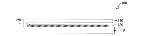
- the organic EL display device 100 manufactured in this embodiment includes an organic EL element 120 connected to a TFT 112, an adhesive layer on a TFT substrate 110 provided with a TFT 112 (see FIG. 10). 130 and the sealing substrate 140 have the structure provided in this order.
- the organic EL element 120 includes a pair of substrates (TFT substrates) by bonding a TFT substrate 110 on which the organic EL element 120 is laminated to a sealing substrate 140 using an adhesive layer 130. 110, sealing substrate 140).
- TFT substrates substrates
- the organic EL element 120 is sealed between the TFT substrate 110 and the sealing substrate 140 as described above, so that oxygen or moisture can enter the organic EL element 120 from the outside. It is prevented.
- the TFT substrate 110 includes a transparent insulating substrate 111 such as a glass substrate as a supporting substrate.
- a plurality of wirings 114 each including a plurality of gate lines laid in the horizontal direction and a plurality of signal lines laid in the vertical direction and intersecting the gate lines are provided. It has been.
- a gate line driving circuit (not shown) for driving the gate line is connected to the gate line, and a signal line driving circuit (not shown) for driving the signal line is connected to the signal line.
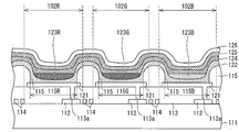
- the organic EL display device 100 is a full-color active matrix type organic EL display device. On the insulating substrate 111, red (R), green (G), and blue are shown in regions surrounded by the wirings 114, respectively.
- the sub-pixels 102R, 102G, and 102B of the respective colors including the organic EL elements 120 of the respective colors (B) are arranged in a matrix.
- a region surrounded by these wirings 114 is one subpixel (dot), and R, G, and B light emitting regions are defined for each subpixel.
- the pixel (that is, one pixel) has three sub-pixels: a red sub-pixel 102R that transmits red light, a green sub-pixel 102G that transmits green light, and a blue sub-pixel 102B that transmits blue light. 102R / 102G / 102B.
- Each of the sub-pixels 102R, 102G, and 102B includes openings 115R and 115G that are covered with stripe-shaped light-emitting layers 123R, 123G, and 123B as light-emitting regions of the respective colors that emit light in the sub-pixels 102R, 102G, and 102B. -115B is provided.
- the light emitting layers 123R, 123G, and 123B are patterned by vapor deposition for each color.
- the openings 115R, 115G, and 115B will be described later.
- These sub-pixels 102R, 102G, and 102B are provided with TFTs 112 connected to the first electrode 121 in the organic EL element 120, respectively.
- the light emission intensity of each of the sub-pixels 102R, 102G, and 102B is determined by scanning and selection by the wiring 114 and the TFT 112.
- the organic EL display device 100 realizes image display by selectively causing the organic EL element 120 to emit light with a desired luminance using the TFT 112.
- the TFT substrate 110 will be described.
- the TFT substrate 110 has a TFT 112 (switching element), an interlayer film 113 (interlayer insulating film, planarization film), a wiring 114, and an edge cover 115 on a transparent insulating substrate 111 such as a glass substrate. It has the structure formed in this order.
- TFTs 112 are provided corresponding to the sub-pixels 102R, 102G, and 102B, respectively.
- the structure of the TFT is conventionally well known. Therefore, illustration and description of each layer in the TFT 112 are omitted.
- the interlayer film 113 is laminated on the insulating substrate 111 over the entire area of the insulating substrate 111 so as to cover the TFTs 112.
- the first electrode 121 in the organic EL element 120 is formed.
- the interlayer film 113 is provided with a contact hole 113a for electrically connecting the first electrode 121 in the organic EL element 120 to the TFT 112. Thereby, the TFT 112 is electrically connected to the organic EL element 120 through the contact hole 113a.
- the edge cover 115 detects that the first electrode 121 and the second electrode 126 in the organic EL element 120 are short-circuited when the organic EL layer becomes thin or the electric field concentration occurs at the pattern end of the first electrode 121. It is an insulating layer for preventing.
- the edge cover 115 is formed on the interlayer film 113 so as to cover the pattern end of the first electrode 121.
- the edge cover 115 is provided with openings 115R, 115G, and 115B for each of the sub-pixels 102R, 102G, and 102B.
- the openings 115R, 115G, and 115B of the edge cover 115 serve as light emitting regions of the sub-pixels 102R, 102G, and 102B.
- the sub-pixels 102R, 102G, and 102B are partitioned by the edge cover 115 having an insulating property.
- the edge cover 115 also functions as an element isolation film.
- the organic EL element 120 is a light emitting element that can emit light with high luminance by low-voltage direct current drive, and a first electrode 121, an organic EL layer, and a second electrode 126 are stacked in this order.
- the first electrode 121 is a layer having a function of injecting (supplying) holes into the organic EL layer. As described above, the first electrode 121 is connected to the TFT 112 through the contact hole 113a.
- a hole injection layer / hole transport layer 122, light emitting layers 123R, 123G, 123B, the electron carrying layer 124, and the electron injection layer 125 have the structure formed in this order.
- the stacking order is that in which the first electrode 121 is an anode and the second electrode 126 is a cathode, and when the first electrode 121 is a cathode and the second electrode 126 is an anode, the organic EL layer is used. The order of stacking is reversed.
- the hole injection layer is a layer having a function of increasing the hole injection efficiency into the light emitting layers 123R, 123G, and 123B.
- the hole transport layer is a layer having a function of improving the efficiency of transporting holes to the light emitting layers 123R, 123G, and 123B.
- the hole injection / hole transport layer 122 is uniformly formed on the entire display region of the TFT substrate 110 so as to cover the first electrode 121 and the edge cover 115.
- the hole injection layer / hole transport layer 122 in which the hole injection layer and the hole transport layer are integrated is provided as the hole injection layer and the hole transport layer.
- An example will be described.
- the present embodiment is not limited to this.
- the hole injection layer and the hole transport layer may be formed as independent layers.
- the light emitting layers 123R, 123G, and 123B correspond to the sub-pixels 102R, 102G, and 102B so as to cover the openings 115R, 115G, and 115B of the edge cover 115, respectively. Is formed.
- the light emitting layers 123R, 123G, and 123B are layers having a function of emitting light by recombining holes injected from the first electrode 121 side with electrons injected from the second electrode 126 side. .
- the light emitting layers 123R, 123G, and 123B are each formed of a material having high light emission efficiency, such as a low molecular fluorescent dye or a metal complex.
- the electron transport layer 124 is a layer having a function of increasing the electron transport efficiency from the second electrode 126 to the light emitting layers 123R, 123G, and 123B.
- the electron injection layer 125 is a layer having a function of increasing the electron injection efficiency from the second electrode 126 to the light emitting layers 123R, 123G, and 123B.
- the electron transport layer 124 is formed on the light emitting layer 123R / 123G / 123B and the hole injection layer / hole transport layer 122 so as to cover the light emitting layer 123R / 123G / 123B and the hole injection layer / hole transport layer 122.
- the TFT substrate 110 is uniformly formed over the entire display area.
- the electron injection layer 125 is uniformly formed on the entire surface of the display region of the TFT substrate 110 on the electron transport layer 124 so as to cover the electron transport layer 124.
- the electron transport layer 124 and the electron injection layer 125 may be formed as independent layers as described above, or may be provided integrally with each other. That is, the organic EL display device 100 may include an electron transport layer / electron injection layer instead of the electron transport layer 124 and the electron injection layer 125.
- the second electrode 126 is a layer having a function of injecting electrons into the organic EL layer composed of the organic layers as described above.
- the second electrode 126 is uniformly formed on the electron injection layer 125 over the entire display region of the TFT substrate 110 so as to cover the electron injection layer 125.
- organic layers other than the light-emitting layers 123R, 123G, and 123B are not essential layers as the organic EL layer, and may be appropriately formed according to the required characteristics of the organic EL element 120.
- a carrier blocking layer can also be added to the organic EL layer as necessary. For example, by adding a hole blocking layer as a carrier blocking layer between the light emitting layers 123R, 123G, and 123B and the electron transport layer 124, holes are prevented from passing through the electron transport layer 124, thereby improving luminous efficiency. can do.
- first electrode / light emitting layer / second electrode (2) First electrode / hole transport layer / light emitting layer / electron transport layer / second electrode (3) First electrode / hole transport layer / light emitting layer / Hole blocking layer (carrier blocking layer) / electron transport layer / second electrode (4) first electrode / hole transport layer / light emitting layer / hole blocking layer / electron transport layer / electron injection layer / second electrode (5 ) 1st electrode / hole injection layer / hole transport layer / light emitting layer / electron transport layer / electron injection layer / second electrode (6) 1st electrode / hole injection layer / hole transport layer / light emitting layer / positive Hole blocking layer / electron transport layer / second electrode (7) first electrode / hole injection layer / hole transport layer / light emitting layer / hole blocking layer / electron transport layer / electron injection layer / second electrode (8) 1st electrode
- the configuration of the organic EL element 120 is not limited to the above-described exemplary layer configuration, and a desired layer configuration can be adopted according to the required characteristics of the organic EL element 120 as described above.
- FIG. 11 is a flowchart showing the manufacturing process of the organic EL display device 100 in the order of steps.
- the manufacturing method of the organic EL display device 100 includes, for example, a TFT substrate / first electrode manufacturing step (S1), a hole injection layer / hole transport layer deposition configuration (S2). ), A light emitting layer vapor deposition step (S3), an electron transport layer vapor deposition step (S4), an electron injection layer vapor deposition step (S5), a second electrode vapor deposition step (S6), and a sealing step (S7).
- the stacking order described in the present embodiment uses the first electrode 121 as an anode and the second electrode 126 as a cathode, and conversely, uses the first electrode 121 as a cathode and the second electrode 126. Is used as the anode, the stacking order of the organic EL layers is reversed. Similarly, the materials constituting the first electrode 121 and the second electrode 126 are also inverted.
- a photosensitive resin is applied on an insulating substrate 111 such as glass on which TFTs 112 and wirings 114 are formed by a known technique, and patterning is performed by a photolithography technique, thereby insulating substrate 111.
- An interlayer film 113 is formed thereon.
- the insulating substrate 111 has, for example, a thickness of 0.7 to 1.1 mm, a length in the y-axis direction (vertical length) of 400 to 500 mm, and a length in the x-axis direction (horizontal length) of 300.
- a glass substrate or a plastic substrate of ⁇ 400 mm is used. In this embodiment, a glass substrate is used.
- an acrylic resin or a polyimide resin can be used as the interlayer film 113.
- the acrylic resin include Optomer series manufactured by JSR Corporation.
- a polyimide resin the photo nice series by Toray Industries, Inc. is mentioned, for example.
- the polyimide resin is generally not transparent but colored. Therefore, when a bottom emission type organic EL display device is manufactured as the organic EL display device 100 as shown in FIG. 10, a transparent resin such as an acrylic resin is more preferably used as the interlayer film 113. Used.
- the film thickness of the interlayer film 113 is not particularly limited as long as the step due to the TFT 112 can be compensated. In this embodiment, for example, the thickness is about 2 ⁇ m.
- a contact hole 113 a for electrically connecting the first electrode 121 to the TFT 112 is formed in the interlayer film 113.
- an ITO (Indium Tin Oxide: Indium Tin Oxide) film is formed with a thickness of 100 nm by a sputtering method or the like.
- the ITO film is etched using ferric chloride as an etchant. Thereafter, the photoresist is stripped using a resist stripping solution, and substrate cleaning is further performed. As a result, the first electrodes 121 are formed in a matrix on the interlayer film 113.
- Examples of the conductive film material used for the first electrode 121 include transparent conductive materials such as ITO, IZO (Indium Zinc Oxide), gallium-doped zinc oxide (GZO), gold (Au), Metal materials such as nickel (Ni) and platinum (Pt) can be used.
- transparent conductive materials such as ITO, IZO (Indium Zinc Oxide), gallium-doped zinc oxide (GZO), gold (Au), Metal materials such as nickel (Ni) and platinum (Pt) can be used.
- a method for laminating the conductive film in addition to the sputtering method, a vacuum deposition method, a CVD (chemical vapor deposition) method, a plasma CVD method, a printing method, or the like can be used.
- the thickness of the first electrode 121 is not particularly limited, it can be set to, for example, a thickness of 100 nm as described above.
- the edge cover 115 is patterned and formed with a film thickness of about 1 ⁇ m, for example.
- an insulating material similar to that of the interlayer film 113 can be used.
- the TFT substrate 110 and the first electrode 121 are manufactured (S1).
- the TFT substrate 110 that has undergone the above-described steps is subjected to oxygen plasma treatment as a vacuum baking for dehydration and surface cleaning of the first electrode 121.
- a hole injection layer and a hole transport layer are displayed on the TFT substrate 110 on the TFT substrate 110 using a conventional deposition apparatus. Vapor deposition is performed on the entire area (S2).
- an open mask having an entire display area opened is aligned and adhered to the TFT substrate 110 and then scattered from the evaporation source while rotating the TFT substrate 110 and the open mask together. Vapor deposition particles are uniformly deposited on the entire display region through the opening of the open mask.
- vapor deposition on the entire surface of the display area means that vapor deposition is performed continuously between adjacent sub-pixels of different colors.
- Examples of the material for the hole injection layer and the hole transport layer include benzine, styrylamine, triphenylamine, porphyrin, triazole, imidazole, oxadiazole, polyarylalkane, phenylenediamine, arylamine, oxazole, anthracene, and fluorenone. , Hydrazone, stilbene, triphenylene, azatriphenylene, and derivatives thereof, polysilane compounds, vinylcarbazole compounds, thiophene compounds, aniline compounds, etc., heterocyclic or chain conjugated monomers, oligomers, or polymers , Etc.
- the hole injection layer and the hole transport layer may be integrated as described above, or may be formed as independent layers.
- Each film thickness is, for example, 10 to 100 nm.
- the hole injection layer / hole transport layer 122 is provided as the hole injection layer and the hole transport layer, and 4,4′-bis [ N- (1-naphthyl) -N-phenylamino] biphenyl ( ⁇ -NPD) was used.
- the film thickness of the hole injection layer / hole transport layer 122 was 30 nm.
- the light emitting layers 123R, 123G, and 102B corresponding to the sub-pixels 102R, 102G, and 102B are formed on the hole injection layer / hole transport layer 122 so as to cover the openings 115R, 115G, and 115B of the edge cover 115.
- 123B is separately formed (pattern formation) (S3).
- the light emitting layers 123R, 123G, and 123B are made of a material having high luminous efficiency such as a low molecular fluorescent dye or a metal complex.
- Examples of materials for the light emitting layers 123R, 123G, and 123B include anthracene, naphthalene, indene, phenanthrene, pyrene, naphthacene, triphenylene, anthracene, perylene, picene, fluoranthene, acephenanthrylene, pentaphen, pentacene, coronene, butadiene, and coumarin.
- the film thickness of the light emitting layers 123R, 123G, and 123B is, for example, 10 to 100 nm.
- the vapor deposition method and the vapor deposition apparatus according to the present embodiment can be particularly preferably used for such separate formation (pattern formation) of the light emitting layers 123R, 123G, and 123B.
- the electron transport layer 124, the hole injection layer / hole transport layer 122 and the light emitting layers 123R, 123G, 123B are formed.
- the entire surface of the display area of the TFT substrate 110 is deposited so as to cover (S4).
- the electron injection layer 125 is applied to the entire surface of the display region of the TFT substrate 110 so as to cover the electron transport layer 124 by the same method as the hole injection layer / hole transport layer deposition step (S2) described above. Evaporation is performed (S5).
- Examples of the material for the electron transport layer 124 and the electron injection layer 125 include tris (8-quinolinolato) aluminum complex, oxadiazole derivative, triazole derivative, phenylquinoxaline derivative, silole derivative, and the like.
- Alq tris (8-hydroxyquinoline) aluminum
- anthracene naphthalene
- phenanthrene pyrene
- anthracene perylene
- butadiene coumarin
- acridine stilbene
- 1,10-phenanthroline and derivatives and metal complexes thereof
- LiF LiF
- the electron transport layer 124 and the electron injection layer 125 may be integrated or formed as independent layers.
- Each film thickness is, for example, 1 to 100 nm.
- the total film thickness of the electron transport layer 124 and the electron injection layer 125 is, for example, 20 to 200 nm.
- Alq is used as the material of the electron transport layer 124
- LiF is used as the material of the electron injection layer 125.
- the thickness of the electron transport layer 124 was 30 nm
- the thickness of the electron injection layer 125 was 1 nm.
- the second electrode 126 is applied to the entire surface of the display region of the TFT substrate 110 so as to cover the electron injection layer 125 by the same method as in the hole injection layer / hole transport layer deposition step (S2). Evaporation is performed (S6).
- Electrode material of the second electrode 126 a metal having a small work function is preferably used.
- examples of such electrode materials include magnesium alloys (MgAg, etc.), aluminum alloys (AlLi, AlCa, AlMg, etc.), metallic calcium, and the like.
- the thickness of the second electrode 126 is, for example, 50 to 100 nm.
- the organic EL element 120 composed of the organic EL layer, the first electrode 121, and the second electrode 126 was formed on the TFT substrate 110.
- the TFT substrate 110 on which the organic EL element 120 was formed and the sealing substrate 140 were bonded together with an adhesive layer 130, and the organic EL element 120 was sealed.
- sealing substrate 140 for example, an insulating substrate such as a glass substrate or a plastic substrate having a thickness of 0.4 to 1.1 mm is used. In this embodiment, a glass substrate is used.
- the vertical length and horizontal length of the sealing substrate 140 may be appropriately adjusted according to the size of the target organic EL display device 100, and an insulating substrate having substantially the same size as the insulating substrate 111 in the TFT substrate 110 is used. After sealing the organic EL element 120, the organic EL element 120 may be divided according to the size of the target organic EL display device 100.
- sealing method of the organic EL element 120 it is not limited to an above-described method.
- Other sealing methods include, for example, a method of using engraved glass as the sealing substrate 140 and sealing in a frame shape with a sealing resin, frit glass, or the like, or between the TFT substrate 110 and the sealing substrate 140.
- a method of filling the resin in between The manufacturing method of the organic EL display device 100 does not depend on the sealing method, and any sealing method can be applied.
- a protective film (not shown) that prevents oxygen and moisture from entering the organic EL element 120 from the outside is provided on the second electrode 126 so as to cover the second electrode 126. Good.
- the protective film is made of an insulating or conductive material. Examples of such a material include silicon nitride and silicon oxide. Further, the thickness of the protective film is, for example, 100 to 1000 nm.
- the organic EL display device 100 is completed through the above steps.
- a predetermined image is displayed by controlling the light emission luminance of each of the sub-pixels 102R, 102G, and 102B.
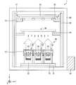
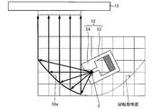
- FIG. 1 is a schematic diagram of a vapor deposition apparatus 1 according to the present embodiment.
- the insulating substrate 111 in FIG. 10 is an example of the deposition target substrate 10 in FIG. 1.
- the vapor deposition apparatus 1 is an apparatus that deposits vapor deposition particles on a predetermined region (hereinafter referred to as a vapor deposition film formation target region) of the deposition target substrate 10, and vapor deposition particles that inject the vapor deposition particles toward the deposition target substrate 10. It has the injection
- the vapor deposition film formation target surface in the claims is a surface having a vapor deposition film formation target region.
- the vapor deposition mask 20 and the vapor deposition particle injection mechanism 84 are disposed to face each other with a certain gap (gap) (that is, separated by a certain distance).
- gap a certain gap
- the vapor deposition mask 20 is made of, for example, a metal member.
- the vapor deposition mask 20 is a rectangular (band-shaped) vapor deposition mask in which at least one side is formed shorter than the width of the vapor deposition film formation target region of the deposition target substrate 10.
- the vapor deposition mask 20 has an opening (through hole) 21 corresponding to a film formation pattern to be formed on the film formation substrate 10.
- the opening 21 has a strip shape
- the vapor deposition mask 20 has a stripe-shaped opening pattern in which a plurality of the openings 21 are arranged in one direction (here, the long side direction of the vapor deposition mask 20).
- the openings 21 are formed so as to be long in the short side direction of the vapor deposition mask 20, and a plurality of openings 21 are provided side by side in the long side direction of the vapor deposition mask 20.
- the deposition target substrate 10 is scanned in the short side direction (scanning direction) of the vapor deposition mask 20 while fixing the relative position between the vapor deposition mask 20 and the vapor deposition particle injection mechanism 84. As a result, a predetermined stripe-shaped vapor deposition pattern is formed in the vapor deposition film formation target region of the deposition target substrate 10.
- the deposition mask 20 and the vapor deposition particle ejection mechanism 84 are fixed to the deposition substrate 10 while the relative position relationship between the vapor deposition mask 20 and the vapor deposition particle ejection mechanism 84 is maintained with the deposition substrate 10 fixed. You may make it move. Alternatively, both the deposition target substrate 10, the vapor deposition mask 20, and the vapor deposition particle injection mechanism 84 may be moved.
- the present invention is not limited to a vapor deposition apparatus of a type that deposits vapor deposition particles on the film formation substrate 10 by moving at least one of the film formation substrate 10 and the vapor deposition mask 20 relative to the other.
- the deposition mask 20 has an area equal to or larger than the deposition film formation target region of the deposition target substrate 10 and can be applied to a deposition apparatus in which the deposition target substrate 10 and the deposition mask 20 are fixed. Is possible.
- the vapor deposition mask 20 having the above configuration can be omitted when a solid pattern is formed on the deposition target substrate 10.
- the vapor deposition particle injection mechanism 84 is disposed below the film formation substrate 10, and the film formation substrate 10 is held with the vapor deposition film formation target region facing downward.
- the vapor deposition particle injection mechanism 84 deposits vapor deposition particles on the vapor deposition film formation target region of the deposition target substrate 10 from below through the opening 21 of the vapor deposition mask 20.
- the vapor deposition particle injection mechanism 84 includes a plurality of crucibles 50.
- the plurality of crucibles 50 are arranged in a line along the arrangement direction of the openings 21 of the vapor deposition mask 20.
- the plurality of crucibles 50 have substantially the same configuration, and have an injection port 86 for injecting (scattering) vapor deposition particles on the surface facing the vapor deposition mask 20.
- the crucible 50 is installed such that the injection port 86 faces the opening 21 of the vapor deposition mask 20.
- the injection ports 86 of the crucible 50 are arranged in a line along the direction in which the openings 21 of the vapor deposition mask 20 are arranged in a state of facing the openings 21 of the vapor deposition mask 20.
- the relative positions of the vapor deposition mask 20 and each crucible 50 are fixed. That is, the gap between the surface of the crucible 50 where the injection port 86 is formed and the vapor deposition mask 20 is always kept constant, and the opening 21 of the vapor deposition mask 20 and the injection port 86 of the crucible 50 The relative position of is fixed.
- the injection port 86 of the crucible 50 is disposed so as to be positioned at the center of the opening 21 of the vapor deposition mask 20 when the vapor deposition mask 20 is viewed from the back surface of the deposition target substrate 10 (that is, in plan view). Is preferred.
- FIG. 2 is a diagram showing a specific configuration of the vapor deposition apparatus 1.
- the vapor deposition apparatus 1 includes a chamber 80 and a vacuum pump mechanism 81 as a casing. Except for the vacuum pump mechanism 81, components of the vapor deposition apparatus 1 including the vapor deposition mask 20 and the vapor deposition particle injection mechanism 84 are accommodated in the chamber 80. The deposition target substrate 10 is also set in the chamber 80.
- the vacuum pump mechanism 81 sets the inside of the chamber 80 to a vacuum state (for example, 1.0 ⁇ 10 ⁇ 4 Pa or less). Specifically, the vacuum pump mechanism 81 exhausts the inside of the chamber 80 to a vacuum state via an exhaust port (not shown) provided in the chamber 80 in order to keep the inside of the chamber 80 in a vacuum state during vapor deposition.
- a vacuum state for example, 1.0 ⁇ 10 ⁇ 4 Pa or less.
- the vapor deposition apparatus 1 includes a frame 60, a movable support 61, a fixed support 62, a shutter 40, a movable support 64, a support base 70, and an actuator 75. Have.
- the frame 60 is erected in the chamber 80 and supports the movable support portion 61, the fixed support portion 62, and the movable support portion 64.
- the movable support 61 is supported by the frame 60 at the highest position, and the movable support 64 is supported at the lowest position.
- the movable support unit 61 supports the deposition target substrate 10 in a horizontal posture.
- the movable support portion 61 can be moved in the X-axis direction (the front side of the drawing in FIG. 2) by an unillustrated drive portion (an example of a drive portion in claims) composed of a stepping motor, a roller, a gear, and the like. It has become.
- the drive unit drives the movable support unit 61, the deposition target substrate 10 moves in the X-axis direction.
- the fixed support part 62 supports the vapor deposition mask 20 in a horizontal posture.
- the shutter 40 is a member for blocking the vapor deposition particles ejected from each crucible 50 of the vapor deposition particle ejection mechanism 84 from reaching the deposition target substrate 10.
- a region of the deposition target substrate 10 where a vapor deposition film is not required hereinafter referred to as a vapor deposition film formation unnecessary region
- the shutter 40 is moved to each crucible 50 of the vapor deposition particle injection mechanism 84.
- the movable support part 64 supports the shutter 40.
- the movable support portion 64 can be moved in the X-axis direction (the front side in the drawing of FIG. 1) by a drive unit similar to the movable support portion 61.
- the drive unit drives the movable support unit 64, the shutter 40 moves in the X-axis direction.
- the support base 70 is placed on an actuator 75 installed on the bottom surface of the chamber 80 and supports the vapor deposition particle injection mechanism 84.
- the actuator 75 moves the support base 70 in the X-axis direction.
- the plurality of crucibles 50 constituting the vapor deposition particle injection mechanism 84 are directions perpendicular to both the relative movement direction (X-axis direction) of the deposition target substrate 10 and the normal direction (Z-axis direction) of the deposition target substrate 10. It is arranged along (Y-axis direction).
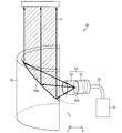
- FIG. 3 is a diagram showing an internal configuration of the crucible 50.
- the crucible 50 has a storage container 51 and an injection container 52.
- the storage container 51 and the injection container 52 are connected via a pipe 55.
- the storage container 51 a solid or liquid vapor deposition material is stored.
- the storage container 51 can be heated by a heater not shown.
- the temperature of the storage container 51 is the temperature at which the vapor deposition material evaporates into vapor deposition particles when the vapor deposition material stored in the storage container 51 is liquid (evaporation). Temperature).
- the temperature of the storage container 51 is set to a temperature higher than the temperature at which the vapor deposition material sublimates to become vapor deposition particles (sublimation temperature).
- the temperature at which the vapor deposition material vaporizes and becomes vapor deposition particles is defined as “vapor deposition particle generation temperature”.
- the vapor deposition material stored in the storage container 51 is vaporized into vapor deposition particles, regardless of whether the vapor deposition material is solid or liquid.
- the vapor deposition particles generated in the storage container 51 are supplied to the injection container 52 via the pipe 55.
- the vapor deposition particle injection mechanism 84 is configured such that vapor deposition particles from the crucible 50 are perpendicularly incident on the deposition target substrate 10. That is, the vapor deposition particle injection mechanism 84 injects a vapor deposition flow parallel to the normal direction of the deposition target substrate 10 from the crucible 50.
- FIG. 4 is an exploded perspective view showing the configuration of the injection container 52.
- the injection container 52 corresponds to a vapor deposition particle injection member, and includes a vapor deposition particle storage member 53 and an injection nozzle member 54. These two members 53 and 54 are joined by, for example, screw machining. It is preferable that the temperature of the vapor deposition particle storage member 53 and the injection nozzle member 54 can be adjusted independently.
- the vapor deposition particle storage member 53 is in the form of a cylindrical container for storing vapor deposition particles in this embodiment.
- the vapor deposition particle storage member 53 of the injection container 52 is connected to the storage container 51 via a pipe 55, and the vapor deposition particles supplied from the storage container 51 are supplied to the vapor deposition particle storage member 53 via the pipe 55. Is done.
- the vapor deposition particle storage member 53 temporarily stores the vapor deposition particles supplied from the storage container 51.
- the injection nozzle member 54 is a member in which an injection port 54a and a rotation inclined surface 54b are formed.
- the rotationally inclined surface 54b is a conical surface, and the conical shape formed by the rotationally inclined surface 54b is set to a shape that improves the utilization efficiency of the vapor deposition material (vapor deposition particles). Is preferred.
- the injection port 54a is provided at the apex of the conical shape formed by the rotation inclined surface 54b.
- the conical shape formed by the rotationally inclined surface 54b has as many vapor deposition particles as possible to be ejected from the injection port 54a, and more preferably, all the vapor deposition particles reach the reflection surface 56a (reflection region) of the reflection member 56 described later.
- the radiation shape is set so as to spread from the exit port 54a at such a radiation angle.
- the crucible 50 includes a reflection member 56 in addition to the storage container 51 and the injection container 52. 2 and 3, the case surrounding the storage container 51, the injection container 52, and the reflection member 56 and the injection port 86 formed on the upper surface of the case are not shown.
- the reflection member 56 has a reflection surface 56 a that reflects the vapor deposition particles emitted from the injection nozzle member 54 toward the vapor deposition film formation target surface of the deposition target substrate 10.
- the reflecting member 56 is installed so that the reflecting surface 56 a faces the injection nozzle member 54 in the crucible 50.
- the relative positional relationship between the reflecting member 56 and the crucible 50 will be described later.
- the temperature of at least the reflecting surface 56a of the reflecting member 56 is controlled by the reflecting member temperature control unit 57 shown in FIG.
- the temperature of at least the reflection surface 56a of the reflection member 56 is set to a temperature higher than the evaporation temperature (deposition particle generation temperature) when vapor deposition particles are generated by evaporating a liquid vapor deposition material in the storage container 51.
- the vapor deposition particles are set to a temperature higher than the sublimation temperature (vapor deposition particle generation temperature).
- the vapor deposition particles are reflected by the reflection surface 56a. More preferably, the temperature of the reflecting surface 56a is set to a temperature at which the vapor deposition particles are completely elastically reflected.
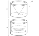
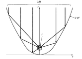
- the reflection surface 56a is formed in a concave curved surface shape.
- the reflecting surface 56a is formed on a rotating paraboloid (parabolic surface) as an example of a concave curved surface shape.
- the reflection surface 56a is formed on one plane when the paraboloid is divided by a plane passing through the apex and the focal point of the paraboloid or the plane parallel to the plane.
- the injection port 54a formed in the injection nozzle member 54 of the crucible 50 is disposed at the position of the focal point F of the paraboloid of revolution.
- FIG. 5 is a diagram for explaining the parabolic principle
- FIG. 6 is a diagram for explaining the function of the reflecting surface 56a in the present embodiment.
- the position of the injection port 54a is defined using this parabola principle. That is, as shown in FIG. 6, the exit port 54a is provided at the focal position of the reflecting surface 56a that is a paraboloid of revolution. Thereby, the reflective surface 56a injects vapor deposition particles in parallel to the normal direction (Z-axis direction) of the deposition target substrate 10.
- the vapor deposition material is vaporized into particles by heating in the storage container 51 of the crucible 50, and the vapor deposition particles are supplied to the injection container 52 of the crucible 50.
- the vapor deposition particles supplied to the injection container 52 are temporarily stored in the vapor deposition particle storage member 53 of the injection container 52 and appropriately discharged from the injection port 54a of the injection nozzle member 54 at a fixed radiation angle.
- the temperature of the reflection surface 56a is set to a predetermined temperature, preferably a temperature at which the vapor deposition particles are completely elastically reflected, so that the vapor deposition particles do not adhere to the reflection surface 56a and are reflected by the reflection surface 56a (including complete elastic reflection). Is done.
- the shape of the reflecting surface 56a is a paraboloid of revolution
- the injection port 54a of the injection nozzle member 54 is disposed at the position of the focal point F of the paraboloid of revolution. Therefore, the vapor deposition particles reflected by the reflecting surface 56 a pass through the injection port 86 toward the vapor deposition mask 20 while being parallel to the normal direction (Z-axis direction) of the deposition target substrate 10.
- the vapor deposition particles that have passed through the opening 21 of the vapor deposition mask 20 reach the vapor deposition film formation target region of the deposition target substrate 10, the vapor deposition particles are vapor deposited on the vapor deposition film formation target region.
- a member that constitutes a vapor deposition source (evaporation particle injection source) in the flow region of the vapor deposition particles between the reflecting member 56 and the deposition target substrate 10. Since the entire structure is disposed, the vapor deposition source component can hinder the flow of the vapor deposition particles.
- the vapor deposition particles are blocked by the vapor deposition source component, and accordingly, an area where the vapor deposition amount is smaller than the surrounding area or an area where no vapor deposition is performed (hereinafter referred to as a shadow area) is generated on the deposition target substrate 10.
- a shadow area an area where the vapor deposition amount is smaller than the surrounding area or an area where no vapor deposition is performed
- the injection container 52 since at least a part of the injection container 52 is installed outside the flow area X of the vapor deposition particles between the reflective surface 56a and the vapor deposition film formation target region, the reflective surface 56a The injection container 52 does not obstruct the flow of the vaporized particles reflected and collimated (vapor deposition flow). As a result, it is possible to prevent or suppress the situation where the film thickness of the vapor deposition film in the vapor deposition film formation target region becomes non-uniform.
- the vapor deposition particles adhere to the injection container 52, the vapor deposition material is not effectively used by the adhering amount. However, in this embodiment, the vapor deposition particles adhere to the injection container 52 and the storage container 51. Since this is avoided, it is also possible to avoid a situation in which the effective utilization rate of the vapor deposition material (a ratio representing how much the vapor deposition material has been effectively utilized without wasting it) is reduced.
- the effective utilization rate of the vapor deposition material is expressed by, for example, “amount of vapor deposition particles vapor deposited on the deposition target substrate 10 / amount of vapor deposition particles injected from the injection container 52”.
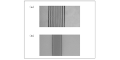
- the inventor of the present application sets the separation distance between the silicon film formation substrate 10 and the vapor deposition mask 20 to 1 mm, and forms a 100 nm vapor deposition film on the film formation substrate 10 with an Alq3 single film. And the vapor deposition apparatus 1 which concerns on this embodiment, respectively, and compared both vapor deposition films. The results of observation with an optical microscope are shown in FIG.
- the film thickness of the film formation pattern was formed evenly over the entire area of the film formation target region of the film formation substrate 10. As a result, it is possible to form a panel with higher display quality than in the prior art.
- the vapor deposition particle storage member 53 that stores the vapor deposition particles is provided corresponding to the injection nozzle member 54.
- the present invention is not limited to this, and a single space for storing the vapor deposition particles is used. You may comprise so that vapor deposition particle
- grains may be distributed to each injection nozzle member. Hereinafter, this specific configuration will be described.
- FIG. 12 is a perspective view schematically showing the external configuration of the crucible 50 ′ according to the present embodiment
- FIG. 13 is a plan view schematically showing the external configuration of the crucible 50 ′.
- the crucible 50 includes a plurality of injection containers 52 and a plurality of reflecting members 56.
- the crucible 50 ′ is a single injection container instead of the plurality of injection containers 52 in the crucible 50 according to the first embodiment. 52 '.
- the crucible 50 ' according to the present embodiment is provided with a plurality of reflecting members 56'.
- the arrangement of the reflection member 56 ' is the same as the arrangement of the reflection member 56 of each crucible 50 in the first embodiment.
- the injection container 52 ′ has an injection nozzle member 54 ′ for injecting vapor deposition particles corresponding to each reflection member 56 ′.
- the crucible 50 ′ has a single storage container 51 ′, and the storage container 51 ′ is connected to the injection container 52 ′ via a pipe 90.
- the storage container 51 ' has a function similar to that of the storage container 51 in the first embodiment.
- the injection container 52 ′ has a space S for temporarily storing the vapor deposition particles supplied from the storage container 51 ′, and the space S is shared by the plurality of injection nozzle members 54 ′. It has become.
- the vapor deposition particles supplied to the space S are ejected from the ejection nozzle member 54 'to the reflecting member 56'.
- the injection container 52 ′ in the present embodiment constitutes the vapor deposition particle injection member in the claims.
- the injection container 52 ′ shown in FIGS. 12 and 13 has a long shape in the arrangement direction of the injection nozzle members 54 ′ in accordance with the plurality of injection nozzle members 54 arranged in one direction. It has a configuration.
- the connection portion between the injection container 52 ′ and the pipe 90, the injection position Due to this positional relationship, it is possible to suppress the occurrence of unevenness in the injection amount of the vapor deposition particles between the injection nozzle members 54 ′.
- the nozzle diameter of the injection nozzle member 54 ′ may be corrected according to the film formation amount for each injection nozzle member 54 ′ obtained by a previously conducted experiment, and the nozzle diameter between the injection nozzle members 54 ′ may be corrected. May be different.
- the injection container 52 ′ and the pipe 90 are connected at a plurality of suitable locations.
- the part on the tank member 53 'side of the pipe 90 may be branched into a plurality of pipes, and each branch part may be connected to an appropriate position of the injection container 52'.
- a plurality of storage containers 51 ′ may be provided, and each storage container 51 ′ and the injection container 52 ′ may be connected by a plurality of pipes 90.
- the injection container 52 ′ is outside the flow region X of the vapor deposition particles between the reflection surface of the reflection member 56 ′ and the vapor deposition film formation target surface of the deposition target substrate (not shown). is set up.
- the injection container 52 ′, the reflection member 56 ′, and the pipe 90 it is desirable to set the injection container 52 ′, the reflection member 56 ′, and the pipe 90 to a temperature higher than the vapor deposition particle generation temperature.
- the storage container 51 ′ may be provided inside the chamber 80 or outside the chamber 80. If the storage container 51 ′ is installed outside the chamber 80, the structure of the chamber 80 can be simplified, and the temperature control of the vapor deposition material is facilitated.
- FIG. 14 is a diagram showing the vapor deposition apparatus 2 according to the present embodiment.
- the same members as those in the above-described embodiment are denoted by the same reference numerals, and differences from the above-described embodiment will be mainly described.
- the vapor deposition apparatus 2 shown in FIG. 14 includes a limiting plate 30 and a fixed support portion 63 in addition to the constituent members of the vapor deposition apparatus 1 including the crucible 50 according to the first embodiment.
- the fixed support portion 63 is supported by the frame 60 between the fixed support portion 62 and the movable support portion 64. Therefore, the limiting plate 30 is disposed between the vapor deposition mask 20 and the shutter 40 and is fixed at that position.
- FIG. 15 is a perspective view showing the arrangement of the deposition target substrate 10, the vapor deposition mask 20, the limiting plate 30, the shutter 40, and the vapor deposition particle injection mechanism 84 in the vapor deposition apparatus 2.
- the limiting plate 30 has an opening 31 that faces the opening 21 of the vapor deposition mask 20.
- the vapor deposition particle injection mechanism 84 the vapor deposition particles injected from the crucible 50 (the injection port 54 a of the injection nozzle member 54, see FIG. 3) pass through the opening 31 of the limiting plate 30 and the opening 21 of the vapor deposition mask 20. A flow path for vapor deposition particles reaching the deposition target substrate 10 is formed.
- the vapor deposition particles reflected by the reflection surface 56a (see FIG. 3) of the reflection member 56 may include vapor deposition particles that are not completely parallel to the normal direction of the deposition target substrate 10. is there.
- the limiting plate 30 removes some of the vapor deposition particles that are not completely parallel as unnecessary vapor deposition particles from the vapor deposition flow injected into the vapor deposition film formation target region of the deposition target substrate 10.
- the limiting plate 30 is set to a temperature lower than the vapor deposition particle generation temperature by a temperature control unit (not shown). In addition, you may provide the cooling mechanism which cools the restriction
- the blurring of the film formation pattern formed on the film formation substrate 10 can be further reduced.
- the inventor of the present application sets the separation distance between the silicon deposition substrate 10 and the vapor deposition mask 20 to 1 mm, and forms a 100 nm Alq3 vapor deposition film (single film) on the deposition target substrate 10.
- Each was formed by the apparatus and the vapor deposition apparatus according to the present example, and both vapor deposition films were compared. The results of observation with an optical microscope are shown in FIG.
- the inventor of the present application produced a large blur of the film formation pattern as shown in FIG. As shown in FIG. 16B, it was confirmed that the pattern blur was improved.
- the vapor deposition film can be formed over the entire region where the vapor deposition film is to be formed on the deposition target substrate 10 without the occurrence of film thickness unevenness in the film formation pattern. As a result, a panel with high display quality can be formed.
- the vapor deposition apparatus in each of the above embodiments was configured to up-deposit (deposit up) vapor deposition particles on the deposition target substrate from below to above through the opening of the vapor deposition mask.
- a deposition apparatus for down deposition (down deposition) in which vapor deposition particles are vapor-deposited on a film formation substrate from the upper side to the lower side through an opening of the vapor deposition mask,
- the present invention can also be applied to a vapor deposition apparatus that causes vapor deposition particles to be side-positioned (side deposit) from the side on the film formation substrate.
- the configuration in which the injection nozzle member is provided one-dimensionally is shown. Therefore, the injection nozzle member may be provided two-dimensionally.
- the number of the injection nozzle members 54 is three, but the number is not limited to this number, and any number is possible. In the case of a vapor deposition apparatus that relatively moves the deposition target substrate 10 and the deposition mask 20 in one direction, the larger the number of injection nozzle members 54, the larger the deposition target substrate 10 can be handled.
- the reflecting surface of the reflecting member is a rotating paraboloid, but it need not be a complete rotating paraboloid, and may be a concave curved surface close to the rotating paraboloid. Further, a part of the reflecting surface may be a paraboloid of revolution.
- the injection port is preferably provided outside the basin.
- the injection port is preferably provided outside the basin.
- the whole of the vapor deposition particle injection member is located outside the basin.
- the entire vapor-deposited particle injection member is located outside the basin.
- the reflecting surface is a rotating paraboloid, and the injection port is provided at a focal position of the rotating paraboloid.
- the reflection surface is a paraboloid of revolution, and the exit is provided at a focal position of the paraboloid of revolution.
- the traveling direction of the vapor deposition particles reflected by the reflecting member can be made parallel to the normal direction of the deposition target substrate.
- parallel includes not only a case where the film is completely parallel to the normal direction of the film formation substrate but also a direction that can be regarded as parallel to the normal direction of the film formation substrate.
- a plurality of the injection ports are provided on a plane parallel to the deposition film formation target surface.
- a plurality of the injection ports are provided on a plane parallel to the vapor deposition film formation target surface.
- the time required to form the vapor deposition film on the surface on which the vapor deposition film is to be formed can be shortened as compared with the case where there is one injection port.
- the temperature of the reflecting surface is higher than the vapor generation particle generation temperature at which the vapor deposition material of the vapor deposition particles vaporizes.
- the temperature of the reflecting surface is higher than a vapor generation particle generation temperature at which the vapor deposition material of the vapor deposition particles vaporizes.
- the vapor deposition particles are completely elastically reflected on the reflecting surface. be able to.
- a vapor deposition apparatus includes any one of the above crucibles.
- the vapor deposition apparatus includes a drive unit that relatively moves the vapor deposition film formation target surface and the crucible.
- the vapor deposition method according to the embodiment of the present invention includes a moving step of relatively moving the vapor deposition film formation target surface, the ejection port, and the reflection surface when vapor deposition particles are ejected.
- the deposition substrate is large, when forming a deposition film with the deposition substrate stationary, a deposition source area that is almost the same size as the deposition substrate is required, and a large number of crucibles are required. Thus, there is a problem that the device cost increases.
- the number of crucibles can be reduced by adopting the above configuration. Thereby, apparatus cost can be reduced.
- the vapor deposition apparatus which concerns on embodiment of this invention is provided with the vapor deposition mask for forming the film-forming pattern of the said vapor deposition film.
- the vapor deposition method according to the embodiment of the present invention includes a vapor deposition mask preparation step of preparing a vapor deposition mask for forming a deposition pattern of the vapor deposition film before the injection step.
- the pixel since the parallelized vapor deposition flow passes through the vapor deposition mask and reaches the vapor deposition film formation target surface, by appropriately setting the size of the vapor deposition particle passage region in the vapor deposition mask, the pixel It becomes possible to form a pattern with a fine unit.
- the vapor deposition apparatus includes a limiting plate for bringing the traveling direction of the vapor deposition particles close to the normal direction of the deposition target substrate.
- the vapor deposition method according to an embodiment of the present invention includes a limiting plate preparation step of preparing a limiting plate for bringing the traveling direction of the vapor deposition particles close to the normal direction of the film formation substrate before the injection step. It is preferable to provide.
- the traveling direction of the vapor deposition particles reflected by the reflecting member further approaches the normal direction of the film formation substrate, it is possible to further parallelize the vapor deposition flow.
- the crucible according to the present invention can be suitably used for, for example, a manufacturing apparatus and a manufacturing method of an organic EL display device used for a film forming process of an organic film in the organic EL display device.
Landscapes
- Chemical & Material Sciences (AREA)
- Engineering & Computer Science (AREA)
- Chemical Kinetics & Catalysis (AREA)
- Materials Engineering (AREA)
- Mechanical Engineering (AREA)
- Metallurgy (AREA)
- Organic Chemistry (AREA)
- Manufacturing & Machinery (AREA)
- Electroluminescent Light Sources (AREA)
Abstract
La présente invention concerne un creuset (50) comprenant : un récipient pour éjection (52) qui est muni d'un orifice d'éjection (54a) pour éjecter des particules de dépôt en phase vapeur dans le but de former un film de dépôt en phase vapeur dans une région de formation de film de dépôt en phase vapeur d'un substrat (10) sur lequel est formé un film. Le creuset comporte également une surface réfléchissante concave (56a) qui réfléchit les particules de dépôt en phase vapeur éjectées par l'orifice d'éjection (54a) en direction de la surface de formation de film de dépôt en phase vapeur. Le récipient pour éjection (52) est conçu de manière qu'au moins une de ses parties soit située à l'extérieur de la zone de flux (X) des particules de dépôt en phase vapeur entre la surface réfléchissante (56a) et la région de formation de film de dépôt en phase vapeur.
Applications Claiming Priority (2)
| Application Number | Priority Date | Filing Date | Title |
|---|---|---|---|
| JP2011-027873 | 2011-02-10 | ||
| JP2011027873 | 2011-02-10 |
Publications (1)
| Publication Number | Publication Date |
|---|---|
| WO2012108363A1 true WO2012108363A1 (fr) | 2012-08-16 |
Family
ID=46638579
Family Applications (1)
| Application Number | Title | Priority Date | Filing Date |
|---|---|---|---|
| PCT/JP2012/052549 Ceased WO2012108363A1 (fr) | 2011-02-10 | 2012-02-03 | Creuset, appareil et procédé de dépôt en phase vapeur et procédé de fabrication d'un dispositif d'affichage électroluminescent organique |
Country Status (1)
| Country | Link |
|---|---|
| WO (1) | WO2012108363A1 (fr) |
Cited By (1)
| Publication number | Priority date | Publication date | Assignee | Title |
|---|---|---|---|---|
| CN111979517A (zh) * | 2020-08-24 | 2020-11-24 | 京东方科技集团股份有限公司 | 温度调节方法及装置、蒸镀设备 |
Citations (5)
| Publication number | Priority date | Publication date | Assignee | Title |
|---|---|---|---|---|
| JPS6059064A (ja) * | 1983-08-20 | 1985-04-05 | ライボルト・アクチエンゲゼルシャフト | 基材上に真空蒸着法で薄層を製造する際に蒸発装置の局部的蒸発パワーを制御するための方法及び装置 |
| JPH04198474A (ja) * | 1990-11-29 | 1992-07-17 | Nkk Corp | イオンプレーティング方法および装置 |
| JPH04346656A (ja) * | 1991-05-21 | 1992-12-02 | Hitachi Ltd | 金属蒸気の加速方法および高速金属蒸気発生装置 |
| JPH0995778A (ja) * | 1995-09-29 | 1997-04-08 | Sony Corp | 真空蒸着装置 |
| JP2008163365A (ja) * | 2006-12-27 | 2008-07-17 | Seiko Epson Corp | 蒸着用坩堝、蒸着法および蒸着装置 |
-
2012
- 2012-02-03 WO PCT/JP2012/052549 patent/WO2012108363A1/fr not_active Ceased
Patent Citations (5)
| Publication number | Priority date | Publication date | Assignee | Title |
|---|---|---|---|---|
| JPS6059064A (ja) * | 1983-08-20 | 1985-04-05 | ライボルト・アクチエンゲゼルシャフト | 基材上に真空蒸着法で薄層を製造する際に蒸発装置の局部的蒸発パワーを制御するための方法及び装置 |
| JPH04198474A (ja) * | 1990-11-29 | 1992-07-17 | Nkk Corp | イオンプレーティング方法および装置 |
| JPH04346656A (ja) * | 1991-05-21 | 1992-12-02 | Hitachi Ltd | 金属蒸気の加速方法および高速金属蒸気発生装置 |
| JPH0995778A (ja) * | 1995-09-29 | 1997-04-08 | Sony Corp | 真空蒸着装置 |
| JP2008163365A (ja) * | 2006-12-27 | 2008-07-17 | Seiko Epson Corp | 蒸着用坩堝、蒸着法および蒸着装置 |
Cited By (2)
| Publication number | Priority date | Publication date | Assignee | Title |
|---|---|---|---|---|
| CN111979517A (zh) * | 2020-08-24 | 2020-11-24 | 京东方科技集团股份有限公司 | 温度调节方法及装置、蒸镀设备 |
| CN111979517B (zh) * | 2020-08-24 | 2022-12-20 | 京东方科技集团股份有限公司 | 温度调节方法及装置、蒸镀设备 |
Similar Documents
| Publication | Publication Date | Title |
|---|---|---|
| JP5623598B2 (ja) | 蒸着装置、蒸着方法、並びに、有機エレクトロルミネッセンス表示装置の製造方法 | |
| US9136310B2 (en) | Thin film deposition apparatus, method of manufacturing organic light-emitting display device by using the apparatus, and organic light-emitting display device manufactured by using the method | |
| KR101760897B1 (ko) | 증착원 및 이를 구비하는 유기막 증착 장치 | |
| TWI540777B (zh) | 薄膜沉積裝置以及使用該裝置製造有機發光顯示元件的方法 | |
| JP5710734B2 (ja) | 蒸着粒子射出装置および蒸着装置 | |
| JP5269256B2 (ja) | 蒸着方法及び蒸着装置 | |
| JP5367195B2 (ja) | 蒸着装置、蒸着方法、及び有機el表示装置の製造方法 | |
| US20120009332A1 (en) | Method of manufacturing organic light-emitting display device | |
| JP6567349B2 (ja) | 蒸着方法及び蒸着装置 | |
| WO2012124512A1 (fr) | Appareil de dépôt en phase vapeur, procédé de dépôt en phase vapeur et dispositif d'affichage électroluminescent organique | |
| WO2012098927A1 (fr) | Appareil de dépôt par évaporation sous vide, procédé de dépôt par évaporation sous vide, élément électroluminescent organique et appareil d'affichage électroluminescent organique | |
| WO2012099011A1 (fr) | Substrat sur lequel une couche est formée, procédé de fabrication et dispositif d'affichage électroluminescent organique | |
| WO2012124564A1 (fr) | Dispositif d'émission de particules de dépôt en phase vapeur, appareil de dépôt en phase vapeur et procédé de dépôt en phase vapeur | |
| WO2012086568A1 (fr) | Dispositif et procédé de dépôt en phase vapeur et procédé de fabrication de dispositifs d'affichage électroluminescents organiques | |
| WO2012099019A1 (fr) | Substrat sur lequel un film est formé, dispositif d'affichage électroluminescent organique et procédé de dépôt par évaporation | |
| WO2012098994A1 (fr) | Substrat sur lequel un film est formé, ainsi que dispositif d'affichage électroluminescent organique | |
| WO2012090777A1 (fr) | Procédé de dépôt, film de dépôt et procédé de production de dispositif d'affichage électroluminescent organique | |
| WO2015083600A1 (fr) | Dispositif de dépôt en phase vapeur, procédé de dépôt en phase vapeur et procédé de fabrication d'élément à électroluminescence organique | |
| CN103476962B (zh) | 蒸镀颗粒射出装置、蒸镀颗粒射出方法和蒸镀装置 | |
| US9614155B2 (en) | Vapor deposition apparatus, vapor deposition method, and method for producing organic electroluminescent element | |
| JP5718362B2 (ja) | 蒸着装置、蒸着方法、並びに、有機エレクトロルミネッセンス表示装置の製造方法 | |
| WO2012108363A1 (fr) | Creuset, appareil et procédé de dépôt en phase vapeur et procédé de fabrication d'un dispositif d'affichage électroluminescent organique |
Legal Events
| Date | Code | Title | Description |
|---|---|---|---|
| 121 | Ep: the epo has been informed by wipo that ep was designated in this application |
Ref document number: 12744249 Country of ref document: EP Kind code of ref document: A1 |
|
| NENP | Non-entry into the national phase |
Ref country code: DE |
|
| 122 | Ep: pct application non-entry in european phase |
Ref document number: 12744249 Country of ref document: EP Kind code of ref document: A1 |
|
| NENP | Non-entry into the national phase |
Ref country code: JP |