WO2012111274A1 - Amplificateur de puissance à haute fréquence - Google Patents
Amplificateur de puissance à haute fréquence Download PDFInfo
- Publication number
- WO2012111274A1 WO2012111274A1 PCT/JP2012/000758 JP2012000758W WO2012111274A1 WO 2012111274 A1 WO2012111274 A1 WO 2012111274A1 JP 2012000758 W JP2012000758 W JP 2012000758W WO 2012111274 A1 WO2012111274 A1 WO 2012111274A1
- Authority
- WO
- WIPO (PCT)
- Prior art keywords
- transistor
- circuit
- resistor
- bias
- base
- Prior art date
- Legal status (The legal status is an assumption and is not a legal conclusion. Google has not performed a legal analysis and makes no representation as to the accuracy of the status listed.)
- Ceased
Links
Images


Classifications
-
- H—ELECTRICITY
- H03—ELECTRONIC CIRCUITRY
- H03F—AMPLIFIERS
- H03F1/00—Details of amplifiers with only discharge tubes, only semiconductor devices or only unspecified devices as amplifying elements
- H03F1/30—Modifications of amplifiers to reduce influence of variations of temperature or supply voltage or other physical parameters
-
- H—ELECTRICITY
- H03—ELECTRONIC CIRCUITRY
- H03F—AMPLIFIERS
- H03F1/00—Details of amplifiers with only discharge tubes, only semiconductor devices or only unspecified devices as amplifying elements
- H03F1/02—Modifications of amplifiers to raise the efficiency, e.g. gliding Class A stages, use of an auxiliary oscillation
- H03F1/0205—Modifications of amplifiers to raise the efficiency, e.g. gliding Class A stages, use of an auxiliary oscillation in transistor amplifiers
- H03F1/0261—Modifications of amplifiers to raise the efficiency, e.g. gliding Class A stages, use of an auxiliary oscillation in transistor amplifiers with control of the polarisation voltage or current, e.g. gliding Class A
-
- H—ELECTRICITY
- H03—ELECTRONIC CIRCUITRY
- H03F—AMPLIFIERS
- H03F1/00—Details of amplifiers with only discharge tubes, only semiconductor devices or only unspecified devices as amplifying elements
- H03F1/30—Modifications of amplifiers to reduce influence of variations of temperature or supply voltage or other physical parameters
- H03F1/302—Modifications of amplifiers to reduce influence of variations of temperature or supply voltage or other physical parameters in bipolar transistor amplifiers
-
- H—ELECTRICITY
- H03—ELECTRONIC CIRCUITRY
- H03F—AMPLIFIERS
- H03F1/00—Details of amplifiers with only discharge tubes, only semiconductor devices or only unspecified devices as amplifying elements
- H03F1/56—Modifications of input or output impedances, not otherwise provided for
- H03F1/565—Modifications of input or output impedances, not otherwise provided for using inductive elements
-
- H—ELECTRICITY
- H03—ELECTRONIC CIRCUITRY
- H03F—AMPLIFIERS
- H03F3/00—Amplifiers with only discharge tubes or only semiconductor devices as amplifying elements
- H03F3/189—High-frequency amplifiers, e.g. radio frequency amplifiers
- H03F3/19—High-frequency amplifiers, e.g. radio frequency amplifiers with semiconductor devices only
- H03F3/191—Tuned amplifiers
-
- H—ELECTRICITY
- H03—ELECTRONIC CIRCUITRY
- H03F—AMPLIFIERS
- H03F3/00—Amplifiers with only discharge tubes or only semiconductor devices as amplifying elements
- H03F3/20—Power amplifiers, e.g. Class B amplifiers, Class C amplifiers
- H03F3/24—Power amplifiers, e.g. Class B amplifiers, Class C amplifiers of transmitter output stages
- H03F3/245—Power amplifiers, e.g. Class B amplifiers, Class C amplifiers of transmitter output stages with semiconductor devices only
-
- H—ELECTRICITY
- H03—ELECTRONIC CIRCUITRY
- H03F—AMPLIFIERS
- H03F2200/00—Indexing scheme relating to amplifiers
- H03F2200/18—Indexing scheme relating to amplifiers the bias of the gate of a FET being controlled by a control signal
-
- H—ELECTRICITY
- H03—ELECTRONIC CIRCUITRY
- H03F—AMPLIFIERS
- H03F2200/00—Indexing scheme relating to amplifiers
- H03F2200/222—A circuit being added at the input of an amplifier to adapt the input impedance of the amplifier
-
- H—ELECTRICITY
- H03—ELECTRONIC CIRCUITRY
- H03F—AMPLIFIERS
- H03F2200/00—Indexing scheme relating to amplifiers
- H03F2200/387—A circuit being added at the output of an amplifier to adapt the output impedance of the amplifier
-
- H—ELECTRICITY
- H03—ELECTRONIC CIRCUITRY
- H03F—AMPLIFIERS
- H03F2200/00—Indexing scheme relating to amplifiers
- H03F2200/555—A voltage generating circuit being realised for biasing different circuit elements
Definitions
- the present invention relates to a high-frequency power amplifier, and more particularly to a high-frequency power amplifier used in mobile communication devices such as mobile phones.
- An OFDM (Orthogonal Frequency Division Multiplexing) system is used as a modulated wave when performing high-speed data communication in a wireless LAN. Since high modulation accuracy is required in a system using OFDM, high linearity is required in a high-frequency power amplifier. To accommodate this, the high frequency power amplifier is designed to have a maximum output that is sufficiently high relative to the power used to obtain sufficient linearity at the power used. On the other hand, in order to increase the maximum output of the high-frequency power amplifier, it is necessary to increase the number of transistors or increase the size, which slows down the thermal response of the amplifier. For this reason, it takes time to stabilize after the amplifier temperature starts to rise due to the heat generated by the amplifying transistor immediately after the amplifier is started. While the temperature rises, the gain and phase of the amplifier change. In OFDM, such a change also causes fatal deterioration of the EVM (Error Vector Magnitude).
- EVM Error Vector Magnitude
- Patent Document 1 Japanese Patent Laid-Open No. 2009-200770
- Japanese Patent Laid-Open No. 2009-200770 has the following disclosure. That is, when the power of the power amplifier is started, the gain of the amplifier is temporarily increased by transiently increasing the bias to the amplifying transistor. Thus, a circuit is shown that shortens the time until temperature fluctuation due to heat generation of the amplification transistor reaches an equilibrium state in the entire circuit.
- FIG. 6 is a circuit diagram shown in Patent Document 1.
- the power amplifier in FIG. 6 includes an amplification transistor 503, a bias circuit 511, a power supply circuit 512, and a speed-up circuit 522.
- the speed-up circuit 522 includes a capacitor 521, a transistor 519, and a transistor 520.
- charge flows into the capacitor 521 when the control voltage for controlling on / off of power amplification rises. Accordingly, current temporarily flows through the collector of the transistor 519 and the collector of the transistor 520, and the potential of the collector of the transistor 519 temporarily decreases. Then, the output voltage of the power supply circuit 512 temporarily increases, and the bias from the bias circuit 511 to the amplification transistor 503 temporarily increases. As a result, the gain of the amplifier temporarily increases, thereby shortening the time until temperature fluctuation due to heat generation of the amplifying transistor reaches an equilibrium state in the entire circuit.
- a high-frequency power amplifier includes a first transistor that amplifies power of a high-frequency signal and a bias circuit that supplies a bias to the first transistor in accordance with a reference voltage. Further, a power supply circuit is provided for applying a reference voltage for controlling a supply amount of bias from the bias circuit to the first transistor to the bias circuit. Further, the control voltage terminal to which a control signal for controlling the start and stop of the bias circuit is applied, and the reference voltage output from the power supply circuit are transiently increased at the rise of the control voltage, so that the first from the bias circuit. And a speed-up circuit for increasing the amount of bias supplied to the transistors.
- the speed-up circuit further includes a capacitor having one end connected to the control voltage terminal, a time constant control circuit connected to the other end of the capacitor, a discharge circuit connected in parallel with the capacitor, a time constant control circuit, and a power source.
- An overshoot control circuit connected to the circuit. Further, the overshoot control circuit determines an increase amount when the reference voltage output from the power supply circuit is transiently increased according to the amount of charge charged in the capacitor. Further, the time constant control circuit determines a time constant at the time of charging / discharging of the capacitor via the time constant control circuit and the overshoot control circuit.
- the capacitor is charged when the control voltage rises, and a charging current due to the charged charge flows to the overshoot control circuit.
- the reference voltage output from the power supply circuit increases transiently, and the bias to the first transistor can be increased transiently.
- the gain of the amplifier increases temporarily, thereby shortening the time until temperature fluctuation due to heat generation of the amplifying transistor reaches an equilibrium state in the entire circuit. Then, it is possible to suppress the degradation of the EVM due to the temperature variation due to the heat generation of the amplification transistor immediately after the amplifier is started.
- the amount of increase in transient bias at the rise of the control voltage can be easily adjusted by adjusting the overshoot control circuit.
- the time constant of the capacitor can be adjusted by the above time constant control circuit, the amount of transient increase in bias at the rise of the control voltage and the time constant until the capacitor charging is completed can be adjusted independently of each other. Can do. This leads to a higher degree of design freedom when adjusting gain fluctuations immediately after the amplifier is started.
- the bias circuit includes a second transistor that supplies a bias to the first transistor, and the overshoot control circuit includes a first resistor having one end grounded. Furthermore, the time constant control circuit includes a third transistor whose emitter is grounded via the first resistor, and a second resistor whose one end is connected to the base of the third transistor. Further, the time constant control circuit includes a fourth transistor having an emitter connected to the base of the third transistor via the second resistor, and a collector connected to the collector of the third transistor and the collector of the second transistor. With. Furthermore, one end of the capacitor is connected to the base of the fourth transistor, and the other end is connected to the control voltage terminal.
- the discharge circuit further includes an FET having a gate grounded, a source connected to the base of the fourth transistor, and a drain connected to the control voltage terminal.
- the power supply circuit includes a third resistor having one end connected to the control voltage terminal and the other end connected to the base of the second transistor.
- the emitter of the second transistor of the bias circuit may be connected to the base of the first transistor, and the base of the second transistor may be grounded via the first resistor.
- the bias circuit includes a first FET that supplies a bias to the first transistor, and the overshoot control circuit includes a first resistor having one end grounded. Furthermore, the time constant control circuit includes a third transistor whose emitter is grounded via the first resistor, and a second resistor whose one end is connected to the base of the third transistor. Further, the time constant control circuit includes a fourth transistor having an emitter connected to the base of the third transistor via the second resistor, and a collector connected to the collector of the third transistor and the drain of the first FET. With. Furthermore, one end of the capacitor is connected to the base of the fourth transistor, and the other end is connected to the control voltage terminal.
- the discharge circuit includes a second FET whose gate is grounded, whose source is connected to the base of the fourth transistor, and whose drain is connected to the control voltage terminal.
- the power supply circuit further includes a third resistor having one end connected to the control voltage terminal and the other end connected to the first FET.
- the source of the first FET of the bias circuit is connected to the base of the first transistor.
- the gate of the first FET may be grounded via the first resistor.
- the overshoot control circuit is configured by a resistor, and by optimizing the resistance value, the reference voltage can be easily set to the above increase amount, and the degree of freedom in design is high.
- the collector is connected to the base of the second transistor, the emitter is connected to the ground via the first resistor, one end is connected to the base of the fifth transistor, and the other And a fourth resistor whose end is grounded.
- the power supply circuit may further include a sixth transistor having a collector connected to the collector of the second transistor, a base connected to the base of the second transistor, and an emitter grounded through the fourth resistor. Good.
- the power supply circuit further includes a fifth transistor having a collector connected to the base of the second transistor and a base connected to the collector.
- the power supply circuit further includes a sixth transistor having a collector connected to the emitter of the fifth transistor, a base connected to the collector, and an emitter connected to the other end of the first resistor.
- the third resistor, the fifth transistor, and the sixth transistor may constitute a temperature compensation circuit that compensates the temperature of the reference voltage.
- the third resistor, the fifth transistor, and the sixth transistor are temperature compensation circuits, and stabilize the bias against temperature changes.
- the time until the temperature fluctuation due to heat generation of the amplification transistor reaches an equilibrium state in the entire circuit is shortened, and deterioration of EVM caused by temperature fluctuation due to heat generation of the amplification transistor immediately after the amplifier is started is suppressed. be able to.
- the amount of increase in transient bias at the rise of the control voltage can be easily adjusted by adjusting the overshoot control circuit.
- the time constant of the capacitor can be adjusted by the above time constant control circuit, the amount of transient increase in bias at the rise of the control voltage and the time constant until the capacitor charging is completed can be adjusted independently of each other. Can do. This leads to a higher degree of design freedom when adjusting gain fluctuations immediately after the amplifier is started.
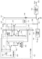
- FIG. 1 is a circuit diagram of a high-frequency power amplifier according to the first embodiment of the present invention.
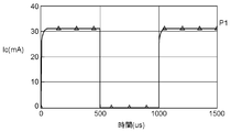
- FIG. 2 is a characteristic diagram showing an example of a transient response characteristic of a comparative example of the first embodiment of the present invention.
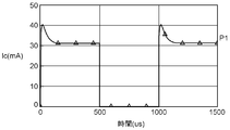
- FIG. 3 is a characteristic diagram showing an example of a transient response characteristic according to the first embodiment of the present invention.
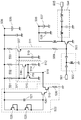
- FIG. 4 is a circuit diagram of a high-frequency power amplifier according to the second embodiment of the present invention.
- FIG. 5 is a circuit diagram of a high-frequency power amplifier according to the third embodiment of the present invention.
- FIG. 6 is a circuit diagram of the power amplifier described in Patent Document 1.
- FIG. 1 is a circuit diagram of a high-frequency power amplifier according to the first embodiment of the present invention.
- the high-frequency power amplifier according to the present embodiment mainly includes the overshoot control circuit 201 to transiently increase the reference voltage Vref for outputting the bias immediately after the control voltage at the control voltage terminal 143 rises. Makes it easy to determine or set the amount of increase.
- the high-frequency amplifier shown in FIG. 1 includes an input terminal 101, an output terminal 105, an input matching circuit 102, an output matching circuit 104, an amplification transistor 103, a stabilization resistor 109, a bias circuit 111, a power supply circuit 112, a speed-up circuit 122, and a collector power supply terminal. 141, a bias power supply terminal 142, a control voltage terminal 143, and a choke coil 144.
- the amplification transistor 103 as the first transistor performs power amplification of the high frequency signal.
- the bias circuit 111 supplies a bias to the amplification transistor 103 according to the reference voltage Vref applied from the power supply circuit 112.
- the bias circuit 111 includes a bias transistor 107 as a second transistor that supplies a bias to the amplification transistor 103.
- the bias transistor 107 supplies a bias corresponding to the reference voltage Vref to the amplification transistor 103.
- the emitter of the bias transistor 107 of the bias circuit 111 is connected to the base of the amplification transistor 103, and the base of the bias transistor 107 is grounded via the overshoot control circuit 201 (resistor 161).
- the power supply circuit 112 applies to the bias circuit 111 a reference voltage Vref that controls the amount of bias supplied from the bias circuit 111 to the amplification transistor 103.
- the power supply circuit 112 includes a resistor 131 as a third resistor having one end connected to the control voltage terminal 143 and the other end connected to the base of the bias transistor 107 that is the second transistor. Further, the power supply circuit 112 includes a transistor 151 that is diode-connected (that is, a collector and a base are short-circuited), and a transistor 152 that is diode-connected. The transistor 151 and the transistor 152 are connected in series so as to be inserted between the resistor 131 and the overshoot control circuit 201. A control signal for controlling the start and stop of the bias circuit 111 is applied to the control voltage terminal 143.
- the speed-up circuit 122 increases the supply amount of bias from the bias circuit 111 to the amplification transistor 103 by transiently increasing the reference voltage Vref output from the power supply circuit 112 when the control voltage rises.
- the speed-up circuit 122 includes a capacitor 121, a time constant control circuit 202, a discharge circuit 203, and an overshoot control circuit 201.
- the capacitor 121 has one end connected to the control voltage terminal 143 and the other end connected to the time constant control circuit 202.
- the discharge circuit 203 is connected in parallel with the capacitor 121.
- the overshoot control circuit 201 determines an increase amount when the reference voltage output from the power supply circuit 112 is transiently increased according to the charge amount charged in the capacitor 121.
- the overshoot control circuit 201 may have a simple circuit configuration including a resistor 161 as a first resistor having one end grounded and the other end connected to the power supply circuit 112.
- the time constant control circuit 202 includes a transistor 119 as a third transistor, a resistor 162 as a second resistor, and a transistor 120 as a fourth transistor.
- the emitter of the transistor 119 is grounded via the first resistor.
- One end of the resistor 162 is connected to the base of the transistor 119.
- the transistor 120 has an emitter connected to the base of the transistor 119 via the resistor 162, and a collector connected to the collector of the transistor 119 and the collector of the bias transistor 107.
- the time constant control circuit 202 determines a time constant at the time of charging / discharging of the capacitor 121 via the time constant control circuit 202 and the overshoot control circuit 201.
- One end of the capacitor 121 is connected to the base of the transistor 120, and the other end is connected to the control voltage terminal 143.
- the discharge circuit 203 includes an FET 163 whose gate is grounded, whose source is connected to the base of the transistor 120, and whose drain is connected to the control voltage terminal 143.
- the input terminal 101 is connected to the base of the amplification transistor 103 via the input matching circuit 102.
- the emitter of the amplification transistor 103 is grounded.
- the collector of the amplification transistor 103 is connected to the collector power supply terminal 141 via the choke coil 144 and connected to the output terminal 105 via the output matching circuit 104.
- the bias circuit 111 includes a bias transistor 107 that biases the amplification transistor 103.
- the collector of the bias transistor 107 is connected to the bias power supply terminal 142, and the emitter is connected to the base of the amplification transistor 103 through the stabilization resistor 109.
- the power supply circuit 112 includes a resistor 131, a transistor 151 as a fifth transistor, and a transistor 152 as a sixth transistor.
- the speed-up circuit 122 includes an overshoot control circuit 201, a time constant control circuit 202, a discharge circuit 203, and a capacitor 121.
- the overshoot control circuit 201 includes a resistor 161, the time constant control circuit 202 includes a transistor 119, a resistor 162, and a transistor 120, and the discharge circuit 203 includes an FET 163.
- One end of the resistor 161 is grounded, the other end is connected to the emitter of the transistor 152 and the emitter of the transistor 119, and the base of the transistor 119 is connected to the emitter of the transistor 120 via the resistor 162.
- the collector of the transistor 120 is connected to the collector of the transistor 119 and the collector of the bias transistor 107.
- One end of the capacitor 121 is connected to the control voltage terminal 143, and the other end is connected to the base of the transistor 120.
- the gate of the FET 163 is grounded, the drain is connected to the control voltage terminal 143, and the source is connected to the base of the transistor 120.
- a high-frequency signal input from the input terminal 101 is input to the amplification transistor 103 via the input matching circuit 102 and is amplified by the amplification transistor 103.
- the amplified high frequency signal is output to the output terminal 105 via the output matching circuit 104.
- the amount of increase in the base potential of the bias transistor 107 immediately after the control voltage rises can be adjusted by the resistance value of the resistor 161. Therefore, the amount of increase in bias can be adjusted independently of the time constant until the capacitor 121 is completely charged. For this reason, the degree of freedom in design when adjusting the transient gain change of the amplifier immediately after the control voltage rises is high. Further, since the charge charged in the capacitor 121 is discharged by the FET 163 when the control voltage falls, even when the capacitance value of the capacitor 121 is small, a sufficient charging current of the capacitor 121 is obtained when the control voltage falls next time. be able to.
- An example of the simulation result is shown.
- the idle current changes immediately after the rise (0 ⁇ s to 50 ⁇ s in FIG. 2) due to the slow thermal response of the amplification transistor 103. This causes changes in gain and phase immediately after the amplifier starts up, and causes distortion and EVM degradation.
- FIG. 3 shows an example of a simulation result of the transient response characteristic of the idle current (collector current Ic) of the amplification transistor in the state where no high-frequency signal is input for the high-frequency power amplifier shown in FIG.
- the current supplied from the bias transistor 107 to the amplification transistor 103 is forcibly increased when the bias rises.
- the capacitance value of the capacitor 121 and the resistance values of the resistors 161 and 162 are designed so as to cancel a transient gain change due to a temperature change immediately after the amplifier starts up.
- the FET 163 discharges the electric charge of the capacitor 121 when the bias falls, in FIG.
- the rise of the Ic of 1000 us realizes the same amount of increase in bias as that of the rise of Ic of 0 us. As a result, it is possible to suppress the degradation of the EVM due to the gain fluctuation at the rise of the amplifier even during the burst operation in which the ON / OFF operation is repeated in a short time.
- FIG. 4 shows a circuit diagram of the high-frequency power amplifier according to the second embodiment.
- the high-frequency power amplifier according to the second embodiment has the same configuration as that of the high-frequency power amplifier according to the first embodiment except for the power supply circuit. The difference will be mainly described.
- the power supply circuit 171 includes a transistor 172 as a fifth transistor, a resistor 175 as a fourth resistor, and a transistor 173 as a sixth transistor.
- the collector is connected to the base of the bias transistor 107, and the emitter is grounded via the resistor 161.
- the resistor 175 has one end connected to the base of the transistor 172 and the other end grounded.
- the transistor 173 has a collector connected to the collector of the bias transistor 107, a base connected to the base of the bias transistor 107, and an emitter grounded through a resistor 175.
- the power supply circuit 171 of the high frequency power amplifier shown in FIG. 4 includes the transistor 172, the transistor 173, the resistor 174, and the resistor 175.
- One end of the resistor 174 is connected to the control voltage terminal 143, and the other end is connected to the base of the bias transistor 107, the base of the transistor 173, and the collector of the transistor 172.
- the collector of the transistor 173 is connected to the collector of the bias transistor 107, the collector of the transistor 119, and the collector of the transistor 120.
- the emitter of the transistor 173 is connected to the base of the transistor 172 and grounded through a resistor 175 having one end grounded.
- the emitter of the transistor 172 is grounded via the resistor 161.
- the power supply circuit 171 also plays a role of temperature compensation and stabilizes the bias against temperature change.
- the high-frequency power amplifier shown in FIG. 4 can adjust the amount of increase in the base potential of the bias transistor 107 immediately after the control voltage rises, by the resistance value of the resistor 161, similarly to the high-frequency power amplifier shown in FIG. Thereby, the amount of increase in bias can be adjusted independently of the time constant until the charging of the capacitor 121 is completed.
- the charge charged in the capacitor 121 is discharged by the FET 163 even when the control voltage falls, similarly to the high-frequency power amplifier shown in FIG. Therefore, even if the capacitance value of the capacitor 121 is small, a sufficient charging current for the capacitor 121 can be obtained at the next rise of the control voltage.
- FIG. 5 shows a circuit diagram of the high-frequency power amplifier according to the third embodiment.
- the high-frequency power amplifier according to the third embodiment has the same configuration as the high-frequency power amplifier according to the first embodiment except for the power supply circuit and the bias circuit. Omitted and the description will focus on the differences.
- the bias circuit 181 includes a bias FET 182 as a first FET that supplies a bias to the amplification transistor 103.
- the source of the bias FET 182 is connected to the base of the amplification transistor 103, and the gate of the bias FET 182 is grounded via the resistor 161.
- the time constant control circuit 202 includes a transistor 119 as a third transistor, a resistor 162 as a second resistor, and a transistor 120 as a fourth transistor.
- the emitter of the transistor 119 is grounded via the resistor 161.
- One end of the resistor 162 is connected to the base of the transistor 119.
- the transistor 120 has an emitter connected to the base of the transistor 119 via the resistor 162, and a collector connected to the collector of the transistor 119 and the drain of the bias FET 182.
- the power supply circuit 191 includes a resistor 192 as a third resistor having one end connected to the control voltage terminal 143 and the other end connected to the bias FET 182.
- the power supply circuit 191 of the high-frequency power amplifier shown in FIG. 5 includes the resistor 192 having one end connected to the control voltage terminal 143.
- the bias circuit 181 includes a bias FET 182.
- the bias FET 182 has a source connected to the base of the amplification transistor 103 via the stabilization resistor 109, and a drain connected to the bias power supply terminal 142.
- the bias FET 182 has a gate connected to the control voltage terminal 143 via the resistor 192 and a gate grounded via the resistor 161.
- the current of the resistor 161 transiently flows when the control voltage rises, so that the potential of the gate of the bias FET 182 rises.
- the bias to the amplification transistor 103 can be increased transiently.
- the resistor 161 may have a fixed resistance value determined according to the use conditions of the high-frequency amplifier, for example, the collector power supply voltage Vcc, the bias voltage Vbias, the base current (bias) of the bias transistor 107, etc.
- a variable resistor may be used.
- the resistor 161 may be a semi-fixed resistor determined by trimming or the like in the manufacturing process.
- the high-frequency power amplifier according to an embodiment of the present invention is small in size, and at the same time, can suppress distortion and deterioration of modulation accuracy due to temperature fluctuation immediately after the amplifier is started up. It can be used for mobile communication devices and the like.
Landscapes
- Engineering & Computer Science (AREA)
- Power Engineering (AREA)
- Amplifiers (AREA)
Abstract
La présente invention se rapporte à un amplificateur de puissance à haute fréquence qui présente une petite taille et un niveau important de liberté de conception en ce qui concerne un changement de gain immédiatement après la mise en route de l'amplificateur. L'amplificateur de puissance à haute fréquence est doté d'un circuit d'accélération (122) qui augmente la quantité de fourniture de polarisation à partir d'un circuit de polarisation vers un transistor d'amplification en augmentant de manière transitoire une tension de référence quand une tension de commande est augmentée. Le circuit d'accélération (122) est doté d'un condensateur (121) et d'un circuit de commande de dépassement (201). Le circuit de commande de dépassement (201) détermine la quantité d'augmentation de la tension de référence lorsque la tension de référence est augmentée de manière transitoire selon une quantité de charge chargée dans le condensateur (121) tout en déterminant la constante de temps du condensateur (121) au cours de la charge et au cours de la décharge.
Priority Applications (2)
| Application Number | Priority Date | Filing Date | Title |
|---|---|---|---|
| JP2012557817A JP5990781B2 (ja) | 2011-02-14 | 2012-02-06 | 高周波電力増幅器 |
| US13/937,218 US8692619B2 (en) | 2011-02-14 | 2013-07-09 | High frequency power amplifier |
Applications Claiming Priority (2)
| Application Number | Priority Date | Filing Date | Title |
|---|---|---|---|
| JP2011-029168 | 2011-02-14 | ||
| JP2011029168 | 2011-02-14 |
Related Child Applications (1)
| Application Number | Title | Priority Date | Filing Date |
|---|---|---|---|
| US13/937,218 Continuation US8692619B2 (en) | 2011-02-14 | 2013-07-09 | High frequency power amplifier |
Publications (1)
| Publication Number | Publication Date |
|---|---|
| WO2012111274A1 true WO2012111274A1 (fr) | 2012-08-23 |
Family
ID=46672221
Family Applications (1)
| Application Number | Title | Priority Date | Filing Date |
|---|---|---|---|
| PCT/JP2012/000758 Ceased WO2012111274A1 (fr) | 2011-02-14 | 2012-02-06 | Amplificateur de puissance à haute fréquence |
Country Status (3)
| Country | Link |
|---|---|
| US (1) | US8692619B2 (fr) |
| JP (1) | JP5990781B2 (fr) |
| WO (1) | WO2012111274A1 (fr) |
Cited By (5)
| Publication number | Priority date | Publication date | Assignee | Title |
|---|---|---|---|---|
| WO2014203439A1 (fr) * | 2013-06-19 | 2014-12-24 | パナソニックIpマネジメント株式会社 | Amplificateur de puissance |
| JP2019220965A (ja) * | 2014-09-10 | 2019-12-26 | スカイワークス ソリューションズ, インコーポレイテッドSkyworks Solutions, Inc. | 無線周波数(rf)電力増幅器バイアス回路 |
| KR20200017854A (ko) * | 2018-08-09 | 2020-02-19 | 삼성전기주식회사 | 응답속도가 개선된 파워 증폭 장치 |
| JP2020028104A (ja) * | 2018-08-16 | 2020-02-20 | サムソン エレクトロ−メカニックス カンパニーリミテッド. | 線形性を改善するためのバイアス回路及び電力増幅装置 |
| JPWO2023188161A1 (fr) * | 2022-03-30 | 2023-10-05 |
Families Citing this family (14)
| Publication number | Priority date | Publication date | Assignee | Title |
|---|---|---|---|---|
| KR101767298B1 (ko) | 2011-05-13 | 2017-08-10 | 스카이워크스 솔루션즈, 인코포레이티드 | 파워 증폭기들을 바이어스하기 위한 장치 및 방법들 |
| US9136802B2 (en) * | 2012-05-17 | 2015-09-15 | Microsemi Corporation | Integrated start-up bias boost for dynamic error vector magnitude enhancement |
| US9154090B2 (en) * | 2012-05-17 | 2015-10-06 | Microsemi Corporation | Integrated start-up bias boost for dynamic error vector magnitude enhancement |
| TWI467916B (zh) * | 2012-11-14 | 2015-01-01 | Universal Scient Ind Shanghai | 電子系統、射頻功率放大器及其溫度補償方法 |
| TWI508432B (zh) * | 2013-06-13 | 2015-11-11 | Advanced Semiconductor Eng | 射頻功率放大器與電子系統 |
| US9632522B2 (en) * | 2015-04-15 | 2017-04-25 | Skyworks Solutions, Inc. | Current mirror bias circuit with voltage adjustment |
| JP2017092526A (ja) * | 2015-11-02 | 2017-05-25 | 株式会社村田製作所 | 電力増幅回路 |
| KR102029553B1 (ko) | 2017-12-22 | 2019-10-07 | 삼성전기주식회사 | 선형성 향상을 위한 바이어스 회로 및 파워 증폭 회로 |
| KR102029558B1 (ko) | 2017-12-27 | 2019-10-07 | 삼성전기주식회사 | 광대역 선형화가 개선된 파워 증폭 장치 |
| US10715093B2 (en) * | 2018-03-09 | 2020-07-14 | Murata Manufacturing Co., Ltd. | Power amplifier module |
| JP2019192987A (ja) * | 2018-04-19 | 2019-10-31 | 株式会社村田製作所 | 電力増幅器の制御回路 |
| KR102585869B1 (ko) * | 2018-10-25 | 2023-10-05 | 삼성전기주식회사 | 선형성을 개선한 증폭 장치 |
| JP7419656B2 (ja) * | 2019-02-05 | 2024-01-23 | 株式会社村田製作所 | 電流制御回路及び電力増幅回路 |
| JP2022150642A (ja) * | 2021-03-26 | 2022-10-07 | 株式会社村田製作所 | 電力増幅回路 |
Citations (4)
| Publication number | Priority date | Publication date | Assignee | Title |
|---|---|---|---|---|
| JP2003338712A (ja) * | 2002-05-20 | 2003-11-28 | Fujitsu Ten Ltd | 高周波電力増幅回路 |
| JP2006093906A (ja) * | 2004-09-22 | 2006-04-06 | Matsushita Electric Ind Co Ltd | 高周波電力増幅器 |
| JP2007504769A (ja) * | 2003-09-08 | 2007-03-01 | スカイワークス ソリューションズ,インコーポレイテッド | 高出力増幅器のための零入力電流制御回路 |
| JP2009200770A (ja) * | 2008-02-21 | 2009-09-03 | Sharp Corp | 電力増幅器 |
Family Cites Families (7)
| Publication number | Priority date | Publication date | Assignee | Title |
|---|---|---|---|---|
| JPH07118614B2 (ja) | 1993-01-14 | 1995-12-18 | 日本電気株式会社 | 増幅器 |
| JP2002280842A (ja) * | 2001-03-21 | 2002-09-27 | Hitachi Ltd | 電力増幅器モジュール |
| JP2005101733A (ja) * | 2003-09-22 | 2005-04-14 | Toshiba Corp | バイアス回路 |
| US7746590B2 (en) | 2004-10-06 | 2010-06-29 | Agere Systems Inc. | Current mirrors having fast turn-on time |
| US7365604B2 (en) * | 2005-12-16 | 2008-04-29 | Mediatek Inc. | RF amplifier with a bias boosting scheme |
| JP4611934B2 (ja) * | 2006-05-26 | 2011-01-12 | 三菱電機株式会社 | 電力増幅器用バイアス回路 |
| US8260224B2 (en) | 2009-12-02 | 2012-09-04 | Sige Semiconductor Inc. | System and method of prebias for rapid power amplifier response correction |
-
2012
- 2012-02-06 WO PCT/JP2012/000758 patent/WO2012111274A1/fr not_active Ceased
- 2012-02-06 JP JP2012557817A patent/JP5990781B2/ja active Active
-
2013
- 2013-07-09 US US13/937,218 patent/US8692619B2/en active Active
Patent Citations (4)
| Publication number | Priority date | Publication date | Assignee | Title |
|---|---|---|---|---|
| JP2003338712A (ja) * | 2002-05-20 | 2003-11-28 | Fujitsu Ten Ltd | 高周波電力増幅回路 |
| JP2007504769A (ja) * | 2003-09-08 | 2007-03-01 | スカイワークス ソリューションズ,インコーポレイテッド | 高出力増幅器のための零入力電流制御回路 |
| JP2006093906A (ja) * | 2004-09-22 | 2006-04-06 | Matsushita Electric Ind Co Ltd | 高周波電力増幅器 |
| JP2009200770A (ja) * | 2008-02-21 | 2009-09-03 | Sharp Corp | 電力増幅器 |
Cited By (11)
| Publication number | Priority date | Publication date | Assignee | Title |
|---|---|---|---|---|
| WO2014203439A1 (fr) * | 2013-06-19 | 2014-12-24 | パナソニックIpマネジメント株式会社 | Amplificateur de puissance |
| US9374039B2 (en) | 2013-06-19 | 2016-06-21 | Panasonic Intellectual Property Management Co., Ltd. | Power amplifier |
| JPWO2014203439A1 (ja) * | 2013-06-19 | 2017-02-23 | パナソニックIpマネジメント株式会社 | 電力増幅器 |
| JP2019220965A (ja) * | 2014-09-10 | 2019-12-26 | スカイワークス ソリューションズ, インコーポレイテッドSkyworks Solutions, Inc. | 無線周波数(rf)電力増幅器バイアス回路 |
| KR20200017854A (ko) * | 2018-08-09 | 2020-02-19 | 삼성전기주식회사 | 응답속도가 개선된 파워 증폭 장치 |
| KR102127808B1 (ko) * | 2018-08-09 | 2020-06-29 | 삼성전기주식회사 | 응답속도가 개선된 파워 증폭 장치 |
| US10903794B2 (en) | 2018-08-09 | 2021-01-26 | Samsung Electro-Mechanics Co., Ltd. | Power amplifier device with improved response speed |
| JP2020028104A (ja) * | 2018-08-16 | 2020-02-20 | サムソン エレクトロ−メカニックス カンパニーリミテッド. | 線形性を改善するためのバイアス回路及び電力増幅装置 |
| US10879853B2 (en) | 2018-08-16 | 2020-12-29 | Samsung Electro-Mechanics Co., Ltd. | Bias circuit and power amplifier for improving linearity |
| JPWO2023188161A1 (fr) * | 2022-03-30 | 2023-10-05 | ||
| WO2023188161A1 (fr) * | 2022-03-30 | 2023-10-05 | 日本電気株式会社 | Dispositif de communication sans fil et procédé de communication sans fil |
Also Published As
| Publication number | Publication date |
|---|---|
| JP5990781B2 (ja) | 2016-09-14 |
| US8692619B2 (en) | 2014-04-08 |
| JPWO2012111274A1 (ja) | 2014-07-03 |
| US20130293311A1 (en) | 2013-11-07 |
Similar Documents
| Publication | Publication Date | Title |
|---|---|---|
| JP5990781B2 (ja) | 高周波電力増幅器 | |
| JP5958774B2 (ja) | 電力増幅モジュール | |
| KR102268387B1 (ko) | 적응형 다중밴드 바이어스 제어 회로 및 파워 증폭 장치 | |
| JP5854372B2 (ja) | 電力増幅モジュール | |
| JP6590323B2 (ja) | 適応形マルチバンド電力増幅装置 | |
| JP2009200770A (ja) | 電力増幅器 | |
| JP6229369B2 (ja) | 電力増幅器 | |
| US9407207B2 (en) | Radio frequency amplifying circuit and power amplifying module | |
| JP5821876B2 (ja) | 電力増幅モジュール | |
| CN111106803B (zh) | 具有改善的线性度的放大设备 | |
| JP6364624B2 (ja) | 電力増幅器 | |
| JP2005526412A (ja) | 能動バイアス回路 | |
| KR20070074661A (ko) | 전력 증폭기 출력 전력의 정밀 제어를 위한 전력 제어 회로 | |
| JP5158425B2 (ja) | Rf電力増幅装置 | |
| JP4330549B2 (ja) | 高周波電力増幅装置 | |
| CN114584080A (zh) | 一种功率放大器及电子设备 | |
| JP6288607B2 (ja) | 電力増幅モジュール | |
| JP4583967B2 (ja) | 高周波電力増幅器及びその出力電力調整方法 | |
| CN111934630B (zh) | 包络跟踪电源调制器及相关的方法和系统 | |
| JP2007048283A (ja) | マルチループ電圧調整器制御スキームにおける零消去 | |
| US20140253244A1 (en) | Power amplifier spurious cancellation | |
| JP2005521286A (ja) | 無線周波出力電力の制御 | |
| JP5757362B2 (ja) | 高周波増幅回路、無線装置 | |
| JP2005184258A (ja) | 高周波増幅器 | |
| CN117397171A (zh) | 发送电路 |
Legal Events
| Date | Code | Title | Description |
|---|---|---|---|
| 121 | Ep: the epo has been informed by wipo that ep was designated in this application |
Ref document number: 12747157 Country of ref document: EP Kind code of ref document: A1 |
|
| ENP | Entry into the national phase |
Ref document number: 2012557817 Country of ref document: JP Kind code of ref document: A |
|
| NENP | Non-entry into the national phase |
Ref country code: DE |
|
| 122 | Ep: pct application non-entry in european phase |
Ref document number: 12747157 Country of ref document: EP Kind code of ref document: A1 |