WO2012111476A1 - Dispositif d'affichage et procédé d'entraînement - Google Patents
Dispositif d'affichage et procédé d'entraînement Download PDFInfo
- Publication number
- WO2012111476A1 WO2012111476A1 PCT/JP2012/052698 JP2012052698W WO2012111476A1 WO 2012111476 A1 WO2012111476 A1 WO 2012111476A1 JP 2012052698 W JP2012052698 W JP 2012052698W WO 2012111476 A1 WO2012111476 A1 WO 2012111476A1
- Authority
- WO
- WIPO (PCT)
- Prior art keywords
- potential
- pixel
- electrode
- pixel electrode
- switching element
- Prior art date
- Legal status (The legal status is an assumption and is not a legal conclusion. Google has not performed a legal analysis and makes no representation as to the accuracy of the status listed.)
- Ceased
Links
Images


Classifications
-
- G—PHYSICS
- G09—EDUCATION; CRYPTOGRAPHY; DISPLAY; ADVERTISING; SEALS
- G09G—ARRANGEMENTS OR CIRCUITS FOR CONTROL OF INDICATING DEVICES USING STATIC MEANS TO PRESENT VARIABLE INFORMATION
- G09G3/00—Control arrangements or circuits, of interest only in connection with visual indicators other than cathode-ray tubes
- G09G3/20—Control arrangements or circuits, of interest only in connection with visual indicators other than cathode-ray tubes for presentation of an assembly of a number of characters, e.g. a page, by composing the assembly by combination of individual elements arranged in a matrix no fixed position being assigned to or needed to be assigned to the individual characters or partial characters
- G09G3/34—Control arrangements or circuits, of interest only in connection with visual indicators other than cathode-ray tubes for presentation of an assembly of a number of characters, e.g. a page, by composing the assembly by combination of individual elements arranged in a matrix no fixed position being assigned to or needed to be assigned to the individual characters or partial characters by control of light from an independent source
- G09G3/36—Control arrangements or circuits, of interest only in connection with visual indicators other than cathode-ray tubes for presentation of an assembly of a number of characters, e.g. a page, by composing the assembly by combination of individual elements arranged in a matrix no fixed position being assigned to or needed to be assigned to the individual characters or partial characters by control of light from an independent source using liquid crystals
- G09G3/3611—Control of matrices with row and column drivers
- G09G3/3648—Control of matrices with row and column drivers using an active matrix
- G09G3/3655—Details of drivers for counter electrodes, e.g. common electrodes for pixel capacitors or supplementary storage capacitors
-
- G—PHYSICS
- G09—EDUCATION; CRYPTOGRAPHY; DISPLAY; ADVERTISING; SEALS
- G09G—ARRANGEMENTS OR CIRCUITS FOR CONTROL OF INDICATING DEVICES USING STATIC MEANS TO PRESENT VARIABLE INFORMATION
- G09G3/00—Control arrangements or circuits, of interest only in connection with visual indicators other than cathode-ray tubes
- G09G3/20—Control arrangements or circuits, of interest only in connection with visual indicators other than cathode-ray tubes for presentation of an assembly of a number of characters, e.g. a page, by composing the assembly by combination of individual elements arranged in a matrix no fixed position being assigned to or needed to be assigned to the individual characters or partial characters
- G09G3/34—Control arrangements or circuits, of interest only in connection with visual indicators other than cathode-ray tubes for presentation of an assembly of a number of characters, e.g. a page, by composing the assembly by combination of individual elements arranged in a matrix no fixed position being assigned to or needed to be assigned to the individual characters or partial characters by control of light from an independent source
- G09G3/36—Control arrangements or circuits, of interest only in connection with visual indicators other than cathode-ray tubes for presentation of an assembly of a number of characters, e.g. a page, by composing the assembly by combination of individual elements arranged in a matrix no fixed position being assigned to or needed to be assigned to the individual characters or partial characters by control of light from an independent source using liquid crystals
- G09G3/3611—Control of matrices with row and column drivers
- G09G3/3614—Control of polarity reversal in general
-
- G—PHYSICS
- G09—EDUCATION; CRYPTOGRAPHY; DISPLAY; ADVERTISING; SEALS
- G09G—ARRANGEMENTS OR CIRCUITS FOR CONTROL OF INDICATING DEVICES USING STATIC MEANS TO PRESENT VARIABLE INFORMATION
- G09G3/00—Control arrangements or circuits, of interest only in connection with visual indicators other than cathode-ray tubes
- G09G3/20—Control arrangements or circuits, of interest only in connection with visual indicators other than cathode-ray tubes for presentation of an assembly of a number of characters, e.g. a page, by composing the assembly by combination of individual elements arranged in a matrix no fixed position being assigned to or needed to be assigned to the individual characters or partial characters
- G09G3/34—Control arrangements or circuits, of interest only in connection with visual indicators other than cathode-ray tubes for presentation of an assembly of a number of characters, e.g. a page, by composing the assembly by combination of individual elements arranged in a matrix no fixed position being assigned to or needed to be assigned to the individual characters or partial characters by control of light from an independent source
- G09G3/36—Control arrangements or circuits, of interest only in connection with visual indicators other than cathode-ray tubes for presentation of an assembly of a number of characters, e.g. a page, by composing the assembly by combination of individual elements arranged in a matrix no fixed position being assigned to or needed to be assigned to the individual characters or partial characters by control of light from an independent source using liquid crystals
- G09G3/3611—Control of matrices with row and column drivers
- G09G3/3648—Control of matrices with row and column drivers using an active matrix
- G09G3/3659—Control of matrices with row and column drivers using an active matrix the addressing of the pixel involving the control of two or more scan electrodes or two or more data electrodes, e.g. pixel voltage dependant on signal of two data electrodes
-
- G—PHYSICS
- G02—OPTICS
- G02F—OPTICAL DEVICES OR ARRANGEMENTS FOR THE CONTROL OF LIGHT BY MODIFICATION OF THE OPTICAL PROPERTIES OF THE MEDIA OF THE ELEMENTS INVOLVED THEREIN; NON-LINEAR OPTICS; FREQUENCY-CHANGING OF LIGHT; OPTICAL LOGIC ELEMENTS; OPTICAL ANALOGUE/DIGITAL CONVERTERS
- G02F1/00—Devices or arrangements for the control of the intensity, colour, phase, polarisation or direction of light arriving from an independent light source, e.g. switching, gating or modulating; Non-linear optics
- G02F1/01—Devices or arrangements for the control of the intensity, colour, phase, polarisation or direction of light arriving from an independent light source, e.g. switching, gating or modulating; Non-linear optics for the control of the intensity, phase, polarisation or colour
- G02F1/13—Devices or arrangements for the control of the intensity, colour, phase, polarisation or direction of light arriving from an independent light source, e.g. switching, gating or modulating; Non-linear optics for the control of the intensity, phase, polarisation or colour based on liquid crystals, e.g. single liquid crystal display cells
- G02F1/133—Constructional arrangements; Operation of liquid crystal cells; Circuit arrangements
- G02F1/1333—Constructional arrangements; Manufacturing methods
- G02F1/1335—Structural association of cells with optical devices, e.g. polarisers or reflectors
- G02F1/133553—Reflecting elements
- G02F1/133555—Transflectors
-
- G—PHYSICS
- G02—OPTICS
- G02F—OPTICAL DEVICES OR ARRANGEMENTS FOR THE CONTROL OF LIGHT BY MODIFICATION OF THE OPTICAL PROPERTIES OF THE MEDIA OF THE ELEMENTS INVOLVED THEREIN; NON-LINEAR OPTICS; FREQUENCY-CHANGING OF LIGHT; OPTICAL LOGIC ELEMENTS; OPTICAL ANALOGUE/DIGITAL CONVERTERS
- G02F1/00—Devices or arrangements for the control of the intensity, colour, phase, polarisation or direction of light arriving from an independent light source, e.g. switching, gating or modulating; Non-linear optics
- G02F1/01—Devices or arrangements for the control of the intensity, colour, phase, polarisation or direction of light arriving from an independent light source, e.g. switching, gating or modulating; Non-linear optics for the control of the intensity, phase, polarisation or colour
- G02F1/13—Devices or arrangements for the control of the intensity, colour, phase, polarisation or direction of light arriving from an independent light source, e.g. switching, gating or modulating; Non-linear optics for the control of the intensity, phase, polarisation or colour based on liquid crystals, e.g. single liquid crystal display cells
- G02F1/133—Constructional arrangements; Operation of liquid crystal cells; Circuit arrangements
- G02F1/136—Liquid crystal cells structurally associated with a semi-conducting layer or substrate, e.g. cells forming part of an integrated circuit
- G02F1/13606—Liquid crystal cells structurally associated with a semi-conducting layer or substrate, e.g. cells forming part of an integrated circuit having means for reducing parasitic capacitance
-
- G—PHYSICS
- G02—OPTICS
- G02F—OPTICAL DEVICES OR ARRANGEMENTS FOR THE CONTROL OF LIGHT BY MODIFICATION OF THE OPTICAL PROPERTIES OF THE MEDIA OF THE ELEMENTS INVOLVED THEREIN; NON-LINEAR OPTICS; FREQUENCY-CHANGING OF LIGHT; OPTICAL LOGIC ELEMENTS; OPTICAL ANALOGUE/DIGITAL CONVERTERS
- G02F1/00—Devices or arrangements for the control of the intensity, colour, phase, polarisation or direction of light arriving from an independent light source, e.g. switching, gating or modulating; Non-linear optics
- G02F1/01—Devices or arrangements for the control of the intensity, colour, phase, polarisation or direction of light arriving from an independent light source, e.g. switching, gating or modulating; Non-linear optics for the control of the intensity, phase, polarisation or colour
- G02F1/13—Devices or arrangements for the control of the intensity, colour, phase, polarisation or direction of light arriving from an independent light source, e.g. switching, gating or modulating; Non-linear optics for the control of the intensity, phase, polarisation or colour based on liquid crystals, e.g. single liquid crystal display cells
- G02F1/133—Constructional arrangements; Operation of liquid crystal cells; Circuit arrangements
- G02F1/136—Liquid crystal cells structurally associated with a semi-conducting layer or substrate, e.g. cells forming part of an integrated circuit
- G02F1/1362—Active matrix addressed cells
- G02F1/136213—Storage capacitors associated with the pixel electrode
-
- G—PHYSICS
- G02—OPTICS
- G02F—OPTICAL DEVICES OR ARRANGEMENTS FOR THE CONTROL OF LIGHT BY MODIFICATION OF THE OPTICAL PROPERTIES OF THE MEDIA OF THE ELEMENTS INVOLVED THEREIN; NON-LINEAR OPTICS; FREQUENCY-CHANGING OF LIGHT; OPTICAL LOGIC ELEMENTS; OPTICAL ANALOGUE/DIGITAL CONVERTERS
- G02F1/00—Devices or arrangements for the control of the intensity, colour, phase, polarisation or direction of light arriving from an independent light source, e.g. switching, gating or modulating; Non-linear optics
- G02F1/01—Devices or arrangements for the control of the intensity, colour, phase, polarisation or direction of light arriving from an independent light source, e.g. switching, gating or modulating; Non-linear optics for the control of the intensity, phase, polarisation or colour
- G02F1/13—Devices or arrangements for the control of the intensity, colour, phase, polarisation or direction of light arriving from an independent light source, e.g. switching, gating or modulating; Non-linear optics for the control of the intensity, phase, polarisation or colour based on liquid crystals, e.g. single liquid crystal display cells
- G02F1/133—Constructional arrangements; Operation of liquid crystal cells; Circuit arrangements
- G02F1/136—Liquid crystal cells structurally associated with a semi-conducting layer or substrate, e.g. cells forming part of an integrated circuit
- G02F1/1362—Active matrix addressed cells
- G02F1/13624—Active matrix addressed cells having more than one switching element per pixel
-
- G—PHYSICS
- G02—OPTICS
- G02F—OPTICAL DEVICES OR ARRANGEMENTS FOR THE CONTROL OF LIGHT BY MODIFICATION OF THE OPTICAL PROPERTIES OF THE MEDIA OF THE ELEMENTS INVOLVED THEREIN; NON-LINEAR OPTICS; FREQUENCY-CHANGING OF LIGHT; OPTICAL LOGIC ELEMENTS; OPTICAL ANALOGUE/DIGITAL CONVERTERS
- G02F2201/00—Constructional arrangements not provided for in groups G02F1/00 - G02F7/00
- G02F2201/52—RGB geometrical arrangements
-
- G—PHYSICS
- G09—EDUCATION; CRYPTOGRAPHY; DISPLAY; ADVERTISING; SEALS
- G09G—ARRANGEMENTS OR CIRCUITS FOR CONTROL OF INDICATING DEVICES USING STATIC MEANS TO PRESENT VARIABLE INFORMATION
- G09G2300/00—Aspects of the constitution of display devices
- G09G2300/04—Structural and physical details of display devices
- G09G2300/0421—Structural details of the set of electrodes
- G09G2300/0426—Layout of electrodes and connections
-
- G—PHYSICS
- G09—EDUCATION; CRYPTOGRAPHY; DISPLAY; ADVERTISING; SEALS
- G09G—ARRANGEMENTS OR CIRCUITS FOR CONTROL OF INDICATING DEVICES USING STATIC MEANS TO PRESENT VARIABLE INFORMATION
- G09G2300/00—Aspects of the constitution of display devices
- G09G2300/08—Active matrix structure, i.e. with use of active elements, inclusive of non-linear two terminal elements, in the pixels together with light emitting or modulating elements
- G09G2300/0809—Several active elements per pixel in active matrix panels
- G09G2300/0833—Several active elements per pixel in active matrix panels forming a linear amplifier or follower
-
- G—PHYSICS
- G09—EDUCATION; CRYPTOGRAPHY; DISPLAY; ADVERTISING; SEALS
- G09G—ARRANGEMENTS OR CIRCUITS FOR CONTROL OF INDICATING DEVICES USING STATIC MEANS TO PRESENT VARIABLE INFORMATION
- G09G2300/00—Aspects of the constitution of display devices
- G09G2300/08—Active matrix structure, i.e. with use of active elements, inclusive of non-linear two terminal elements, in the pixels together with light emitting or modulating elements
- G09G2300/0809—Several active elements per pixel in active matrix panels
- G09G2300/0842—Several active elements per pixel in active matrix panels forming a memory circuit, e.g. a dynamic memory with one capacitor
-
- G—PHYSICS
- G09—EDUCATION; CRYPTOGRAPHY; DISPLAY; ADVERTISING; SEALS
- G09G—ARRANGEMENTS OR CIRCUITS FOR CONTROL OF INDICATING DEVICES USING STATIC MEANS TO PRESENT VARIABLE INFORMATION
- G09G2300/00—Aspects of the constitution of display devices
- G09G2300/08—Active matrix structure, i.e. with use of active elements, inclusive of non-linear two terminal elements, in the pixels together with light emitting or modulating elements
- G09G2300/0876—Supplementary capacities in pixels having special driving circuits and electrodes instead of being connected to common electrode or ground; Use of additional capacitively coupled compensation electrodes
-
- G—PHYSICS
- G09—EDUCATION; CRYPTOGRAPHY; DISPLAY; ADVERTISING; SEALS
- G09G—ARRANGEMENTS OR CIRCUITS FOR CONTROL OF INDICATING DEVICES USING STATIC MEANS TO PRESENT VARIABLE INFORMATION
- G09G2310/00—Command of the display device
- G09G2310/02—Addressing, scanning or driving the display screen or processing steps related thereto
- G09G2310/0243—Details of the generation of driving signals
- G09G2310/0248—Precharge or discharge of column electrodes before or after applying exact column voltages
-
- G—PHYSICS
- G09—EDUCATION; CRYPTOGRAPHY; DISPLAY; ADVERTISING; SEALS
- G09G—ARRANGEMENTS OR CIRCUITS FOR CONTROL OF INDICATING DEVICES USING STATIC MEANS TO PRESENT VARIABLE INFORMATION
- G09G2310/00—Command of the display device
- G09G2310/08—Details of timing specific for flat panels, other than clock recovery
-
- G—PHYSICS
- G09—EDUCATION; CRYPTOGRAPHY; DISPLAY; ADVERTISING; SEALS
- G09G—ARRANGEMENTS OR CIRCUITS FOR CONTROL OF INDICATING DEVICES USING STATIC MEANS TO PRESENT VARIABLE INFORMATION
- G09G2330/00—Aspects of power supply; Aspects of display protection and defect management
- G09G2330/02—Details of power systems and of start or stop of display operation
- G09G2330/021—Power management, e.g. power saving
Definitions
- the present invention relates to a display device, and more particularly to a display device having a configuration in which one pixel is divided into a plurality of sub-pixels in order to improve viewing angle characteristics and a driving method thereof.
- an active matrix liquid crystal display device including a thin film transistor (TFT) as a switching element is known.
- the display portion of the active matrix liquid crystal display device includes a plurality of source bus lines (video signal lines), a plurality of gate bus lines (scanning signal lines), the plurality of source bus lines, and a plurality of gates.
- a plurality of pixel forming portions provided corresponding to the intersections with the bus lines are included. These pixel forming portions are arranged in a matrix to constitute a pixel array.
- FIG. 41 is a circuit diagram showing a configuration of a pixel forming portion of a conventional general active matrix type liquid crystal display device.
- the pixel forming portion includes a thin film transistor T91 having a gate electrode connected to a gate bus line GL passing through a corresponding intersection and a source electrode connected to a source bus line SL passing through the intersection.
- the pixel electrode 92 connected to the drain electrode of the thin film transistor T91, the common electrode (counter electrode) COM and the auxiliary capacitance electrode CS provided in common to the plurality of pixel forming portions, the pixel electrode 92, and the common electrode
- a liquid crystal capacitor Clc formed by COM and an auxiliary capacitor Cstg formed by the pixel electrode 92 and the auxiliary capacitor electrode CS are included.
- a pixel capacitor is formed by the liquid crystal capacitor Clc and the auxiliary capacitor Cstg.
- the auxiliary capacitor Cstg is not necessarily provided.
- FIG. 42 is a circuit diagram showing a configuration example of a pixel formation portion in a conventional liquid crystal display device having a multi-pixel structure. As shown in FIG.
- the pixel formation portion PIX9 is configured by two subpixel portions (a first subpixel portion PIX9a and a second subpixel portion PIX9b).
- Both sub-pixel portions (PIX9a, PIX9b) include transistors (T92, T93), pixel electrodes (E91, E92), liquid crystal capacitors (ClcA, ClcB), and storage capacitors (CstA, CstB) as common components.
- the second sub-pixel portion PIX9b further includes a transistor T94 having a gate electrode connected to the scanning signal line GLi + 1 and a source electrode connected to the pixel electrode E92, and a capacitor connected to the drain electrode of the transistor T94.
- the electrode E93 includes a buffer capacitor Cdown formed by the capacitor electrode E93 and the common electrode (auxiliary capacitor electrode) COM102.
- the potential of the pixel electrode E91 in the first subpixel unit PIX9a is equal to the potential of the pixel electrode E92 in the second subpixel unit PIX9b.
- the transistor T94 is turned on.
- charges move between the pixel electrode E92 and the capacitor electrode E93, and the potential of the pixel electrode E92 varies.
- the pixel electrode E91 and the pixel electrode E92 have different potentials
- the first subpixel unit PIX9a and the second subpixel unit PIX9b have different luminance.
- Japanese Patent Application Laid-Open No. 2009-109600 discloses a liquid crystal display device that can reduce the amplitude of a video signal by amplifying the pixel electrode potential.
- the pixel forming portion is configured as shown in FIG. 43 and the following driving is performed.
- an on-level potential is applied to the line indicated by reference numeral 9 while an off-level potential is applied to the gate bus line GL.
- the thin film transistors T902 and T903 are turned on.
- the video signal potential (the potential of the source bus line SL) is applied to the node 901
- the potential of the common electrode COM is applied to the node 902.
- an on-level potential is applied to the gate bus line GL while an off-level potential is applied to the line indicated by reference numeral 9. Accordingly, the thin film transistor T901 is turned on. As a result, a video signal potential is applied to the node 902. That is, the potential of the node 902 rises from the common electrode potential to the video signal potential. At this time, since the node 901 is in a floating state, the potential of the node 901 increases via the capacitor C91 as the potential of the node 902 increases. As described above, a larger voltage is applied between the pixel electrode and the common electrode.
- the common electrode potential is applied to the node 902 (see FIG. 43) in the first half of one horizontal scanning period. That is, precharge using the common electrode potential is performed. Therefore, the pixel electrode potential is amplified according to the difference between the video signal potential and the common electrode potential.
- the common electrode potential cannot be set freely, the difference between the video signal potential and the common electrode potential cannot be sufficiently increased, and the degree of amplification of the pixel electrode potential is not sufficient.
- the invention disclosed in Japanese Unexamined Patent Publication No. 2009-109600 is applied to a liquid crystal display device having a multi-pixel structure. I can't.
- the amplitude of the video signal cannot be reduced so as to reduce the power consumption for the following reason.
- positive writing when the transistor T94 is turned on, positive charge moves from the storage capacitor CstB to the buffer capacitor Cdown.
- the potential of the pixel electrode E92 in the second subpixel unit PIX9b is lower than the potential of the pixel electrode E91 in the first subpixel unit PIX9a.
- negative polarity writing when the transistor T94 is turned on, positive charges move from the buffer capacitor Cdown to the storage capacitor CstB.
- the potential of the pixel electrode E92 in the second subpixel portion PIX9b is higher than the potential of the pixel electrode E91 in the first subpixel portion PIX9a.
- the liquid crystal applied voltage in the second sub-pixel unit PIX9b is smaller than the liquid crystal applied voltage in the first sub-pixel unit PIX9a in both the frame where the positive polarity writing is performed and the frame where the negative polarity writing is performed.
- a difference voltage between the video signal potential and the common electrode potential is applied to the liquid crystal.
- a voltage smaller than the difference voltage between the video signal potential and the common electrode potential is applied to the liquid crystal.
- an object of the present invention is to realize low power consumption by reducing the amplitude of a video signal in a liquid crystal display device in which one pixel is divided into a plurality of sub-pixels.
- a plurality of video signal lines there are a plurality of video signal lines, a plurality of scanning signal lines intersecting with the plurality of video signal lines, the plurality of video signal lines, and the plurality of scanning signal lines.
- An active matrix type display device having a plurality of pixel forming portions arranged in a matrix corresponding to the intersections with each other and a common electrode provided in common to the plurality of pixel forming portions.
- a selection period including the second period and a non-selection period other than the selection period A constant potential is applied to the corresponding first control wiring, or a constant high level potential and a constant low level potential are alternately applied,
- the corresponding second control wiring is supplied with a potential for turning on the second switching element and the third switching element in the first period, and the second switching element in a period other than the first period.
- a potential to turn off the third switching element is provided,
- a corresponding scanning signal line is given a potential for turning on the first switching element in the second period, and a potential for turning off the first switching element in a period other than the second period. It is characterized by being given.
- the high-level potential and the low-level potential are alternately applied to the first control wiring.
- the corresponding first control wiring includes In a selection period in which a potential lower than the potential of the common electrode is to be applied to the first pixel electrode and the second pixel electrode, the high level potential is applied, The low level potential is applied in a selection period in which a potential higher than the potential of the common electrode is to be applied to the first pixel electrode and the second pixel electrode.
- the corresponding first control wiring includes In a selection period in which a potential lower than the potential of the common electrode is to be applied to the first pixel electrode and the second pixel electrode, the low level potential is applied, The high-level potential is applied in a selection period in which a potential higher than the potential of the common electrode is to be applied to the first pixel electrode and the second pixel electrode.
- the potential of the scanning signal line at the transition from the selection period to the non-selection period is set to a potential lower than the reference potential by an amount equal to the magnitude of the change in potential of the first pixel electrode caused by the change; Selection in which a potential lower than the potential of the second pixel electrode and the potential of the common electrode in a selection period in which a potential higher than the potential of the common electrode is to be applied to the second pixel electrode is to be applied to the second pixel electrode.
- the potential of the first control wiring is set so that a central potential with the potential of the second pixel electrode in the period is equal to the potential of the common electrode.
- a sixth aspect of the present invention is the fifth aspect of the present invention,
- the potential Vctl of the first control wiring is set to a value calculated by the following equation.
- Vctl Vd1 + Vd2 ⁇ Vcom ⁇ Vg2
- Vd1 represents the maximum potential that can be applied to the plurality of video signal lines
- Vd2 represents the minimum potential that can be applied to the plurality of video signal lines
- Vcom represents the potential of the common electrode.
- ⁇ Vg2 represents the magnitude of the change in the potential of the second pixel electrode caused by the change in the potential of the scanning signal line during the transition from the selection period to the non-selection period.
- the first control wiring is arranged to extend in parallel to the scanning signal line.
- the first control wiring is arranged to extend in parallel with the video signal line.
- a two-layer transparent electrode comprising a first transparent electrode functioning as the first pixel electrode and a second transparent electrode including a portion functioning as the second pixel electrode;
- the second capacitor is formed by the first transparent electrode and the second transparent electrode.
- the first transparent electrode is formed in a region between the second transparent electrode and the common electrode, An opening is provided in the center of the first transparent electrode.
- An eleventh aspect of the present invention is the ninth aspect of the present invention,
- the second transparent electrode is formed in a lattice shape so as to have a portion extending in parallel with the scanning signal line and a portion extending in parallel with the video signal line, and the portion functioning as the second pixel electrode is electrically A grid-like electrode part that is separated;
- the grid electrode portion functions as the first control wiring.
- a twelfth aspect of the present invention is the ninth aspect of the present invention,
- the second transparent electrode further includes a shield electrode portion formed in a region between the video signal line and the first transparent electrode and electrically separated from a portion functioning as the second pixel electrode. It is characterized by.
- a thirteenth aspect of the present invention is the twelfth aspect of the present invention,
- the shield electrode portion is formed so as to cover the video signal line.
- a fourteenth aspect of the present invention is the twelfth aspect of the present invention,
- the shield electrode portion does not overlap with the video signal line, and between the video signal line and a portion of the second transparent electrode that functions as the second pixel electrode in a direction in which the scanning signal line extends. It is formed in the area
- a fifteenth aspect of the present invention is the twelfth aspect of the present invention,
- the shield electrode part functions as the first control wiring.
- a sixteenth aspect of the present invention is the ninth aspect of the present invention, Liquid crystal is provided as a display medium between the first pixel electrode and the common electrode and between the second pixel electrode and the common electrode.
- Each pixel forming portion forms a pixel composed of a plurality of regions having different alignment states of the liquid crystal,
- the sub-pixel portion including the first pixel electrode and the sub-pixel portion including the second pixel electrode have the same alignment center.
- Liquid crystal is provided as a display medium between the first pixel electrode and the common electrode and between the second pixel electrode and the common electrode.
- Each pixel forming portion forms a pixel composed of a plurality of regions having different alignment states of the liquid crystal, Of the sub-pixel portion including the first pixel electrode and the sub-pixel portion including the second pixel electrode, the sub-pixel portion to be displayed relatively brightly is disposed at the center of each pixel forming portion.
- Liquid crystal is provided as a display medium between the first pixel electrode and the common electrode and between the second pixel electrode and the common electrode.
- Each pixel forming portion forms a pixel composed of a plurality of regions having different alignment states of the liquid crystal
- the first control wiring is disposed in a region corresponding to a boundary portion of the plurality of regions.
- the plurality of pixel forming portions includes a plurality of color pixel forming portions, Among the plurality of color pixel formation portions, at least one color pixel formation portion has a capacitance value of the second capacitor different from that of the other color pixel formation portions. .
- the plurality of pixel forming portions includes a plurality of color pixel forming portions, For at least one of the plurality of color pixel forming portions, the first control corresponding to the other color pixel forming portions is applied to the corresponding first control wiring. It is characterized by being different from the potential applied to the wiring.
- the amplification circuit unit includes a plurality of amplification stages
- the second conduction terminal of the first switching element is a second conduction terminal of a third switching element included in the amplification stage that is electrically farthest from the second pixel electrode among the plurality of amplification stages.
- the first pixel electrode is included in an amplification stage other than an amplification stage that is electrically closest to the second pixel electrode among the plurality of amplification stages or the second conduction terminal of the first switching element.
- the second pixel electrode is connected to a second conduction terminal of a second switching element included in an amplification stage that is electrically closest to the second pixel electrode among the plurality of amplification stages,
- the second conduction terminal of the second switching element included in the amplification stage disposed electrically away from the second pixel electrode is electrically connected to the second pixel. It is connected to the 2nd conduction terminal of the 3rd switching element contained in the amplification stage arranged near the electrode.
- the display device A first control wiring crossing at least one of the plurality of video signal lines or the plurality of scanning signal lines;
- One step In a state where a potential for turning off the second switching element and the third switching element is applied to the corresponding second control wiring, a potential for turning on the first switching element is applied to the corresponding scanning signal line.
- a potential for turning off the first switching element is applied to the corresponding scanning signal line, and the second switching element and the third switching element are turned off to the corresponding second control wiring. It is characterized in that a potential to be brought into a state is given.
- each pixel forming portion includes a first pixel electrode and a second pixel electrode, and the potentials of the first pixel electrode and the second pixel electrode are changed according to the display image.
- the selection period for this is composed of a first period and a second period.
- the potential of the first pixel electrode is made equal to the potential of the first control wiring in the first period, and then made equal to the video signal potential in the second period.
- the potential of the second pixel electrode is made equal to the video signal potential in the first period, and then amplified in accordance with the difference between the potential of the first control wiring and the video signal potential in the second period.
- the first pixel electrode for example, a sub-pixel for dark display
- the potential of the pixel electrode provided is equal to the video signal potential
- the potential of the second pixel electrode for example, the pixel electrode provided in the sub-pixel for bright display
- the relationship between the difference between the video signal potential and the common electrode potential and the transmittance (described later “ The pseudo VT characteristic ”) can be adjusted as appropriate. This improves the degree of freedom in viewing angle compensation in a display device having a multi-pixel structure.
- the potential of the second pixel electrode is further amplified. For this reason, in a display device having a multi-pixel structure, the amplitude of the video signal can be made significantly smaller than before, and the power consumption is effectively reduced.
- the degree of freedom of viewing angle compensation is improved.
- occurrence of bias in applied voltage to the pixel capacitor between positive and negative polarities in both the dark display pixel and the bright display pixel is suppressed.
- the capacitance value of the second capacitor is extremely larger than the capacitance values of the second first capacitor and the parasitic capacitance, the voltage applied to the pixel capacitor between the positive and negative polarities. It becomes possible to set the potential of the first control wiring relatively easily so as to prevent the occurrence of bias.
- the number of necessary first control wirings is reduced as compared with the configuration in which the first control wirings are arranged so as to extend in parallel with the video signal lines. For this reason, the fall of the aperture ratio by providing a 1st control wiring can be suppressed.
- the same timing is provided from one first control wiring to a plurality of third switching elements.
- no precharge potential is applied.
- the load applied to each first control wiring can be reduced.
- the aperture ratio can be improved and the second capacitor can be set without affecting the aperture ratio. can do.
- the area of the sub-pixel is determined by the area of the opening, and the capacitance value of the second capacitor is the area of the portion where the first transparent electrode and the second transparent electrode overlap (overlapping). Amount). For this reason, the freedom degree regarding the design of the 2nd capacity is secured.
- the transparent electrode formed in a lattice shape functions as the first control wiring. For this reason, the resistance of the first control wiring is reduced, and the aperture ratio can be improved.
- the shield electrode portion is provided in the region between the first transparent electrode and the video signal line, fluctuations in the video signal potential are caused by the potentials of the first pixel electrode and the second pixel electrode. It is possible to reduce the influence on the.
- the shield electrode portion is formed so as to cover the video signal line, the influence of the fluctuation of the video signal potential on the potentials of the first pixel electrode and the second pixel electrode is effective. It becomes possible to reduce it.
- the capacitance formed between the video signal line and the shield electrode portion is relatively small, the fluctuation of the video signal potential is reduced while reducing the wiring capacitance of the video signal line.
- the influence on the potentials of the first pixel electrode and the second pixel electrode can be reduced.
- one electrode functions as both a shield electrode portion and a first control wiring. For this reason, even in a display device having a higher-definition display unit, it is possible to reduce the influence of fluctuations in the video signal potential on the potentials of the first pixel electrode and the second pixel electrode.
- a display device alignment-divided liquid crystal display device
- liquid crystal employed as a display medium and the alignment states of the liquid crystal are different from each other
- the alignment centers of the sub-pixel and the sub-pixel for dark display coincide with each other. For this reason, the number of dark lines can be reduced in the alignment-divided liquid crystal display device. Thereby, the fall of the transmittance
- the sub-pixel for bright display is arranged at the center of each pixel, and suitable display in consideration of the alignment characteristics of the liquid crystal is performed in the alignment-divided liquid crystal display device.
- the first control wiring is formed so as to overlap the dark line. For this reason, the fall of the aperture ratio by providing a 1st control wiring is suppressed effectively.
- the degree of amplification of the potential of the second pixel electrode in the second period can be different for each color. This makes it possible to adjust the viewing angle characteristics more finely.
- the degree of amplification of the potential of the second pixel electrode in the second period can be made different for each color, and the field of view can be more finely divided.
- the angular characteristics can be adjusted.
- the potential of the second pixel electrode is amplified in a plurality of stages during the selection period. For this reason, the amplitude of the video signal can be made significantly smaller than before, and the power consumption is greatly reduced as compared with the conventional one.
- the same effect as in the first aspect of the present invention can be achieved in the method for driving the display device.
- FIG. 6 is an equivalent circuit diagram illustrating a configuration of a typical pixel formation portion (portion for forming one pixel) in the display device of the present invention. It is a signal waveform diagram for demonstrating operation
- 1 is a block diagram showing an overall configuration of an active matrix liquid crystal display device according to a first embodiment of the present invention. In the said 1st Embodiment, it is a figure which shows the arrangement
- FIG. 6 is a diagram for describing a layout in the vicinity of a pixel formation portion in the first embodiment. It is a signal waveform diagram for demonstrating the drive method in the said 1st Embodiment.
- FIG. 6 is a signal waveform diagram for describing an operation of a pixel formation unit in a selection period in the first embodiment. In the said 1st Embodiment, it is a signal waveform diagram for demonstrating the bias
- FIG. 6 is a signal waveform diagram for explaining an example of the operation in the pixel formation portion in the first embodiment. It is a signal waveform diagram for demonstrating the drive method in the 2nd Embodiment of this invention.
- the said 2nd Embodiment it is a signal waveform diagram for demonstrating operation
- it is a signal waveform diagram for demonstrating an example of the operation
- It is a figure which shows the layout of the pixel formation part vicinity in a 1st modification.
- FIG. 10 is a diagram illustrating an arrangement relationship between a pixel formation portion and each line in the first modification example. It is a signal waveform diagram for demonstrating the drive method in the said 1st modification.
- FIG. 20 is a cross-sectional view taken along line AA of FIG. It is a figure which shows the layout of the pixel formation part vicinity in a 3rd modification. It is a figure which shows the layout of the pixel formation part vicinity in a 4th modification. In the said 4th modification, it is a figure which shows the shape of an upper layer transparent electrode and a lower layer transparent electrode. In the 4th modification, it is a figure which shows the arrangement
- FIG. 30 is a cross-sectional view taken along line AA in FIG. 29.
- FIG. 17 is an equivalent circuit diagram including a parasitic capacitance between the source bus line and the transparent electrode and a capacitance formed between the shield electrode and the transparent electrode in the seventh modification example. It is a figure which shows the layout of the pixel formation part vicinity in an 8th modification.
- FIG. 33 is a sectional view taken along line AA in FIG. 32. It is a figure which shows the layout of the pixel formation part vicinity in a 9th modification. It is a figure which shows another example of the layout of the pixel formation part vicinity in a 9th modification. It is a signal waveform diagram for demonstrating the drive method in a 10th modification. It is a signal waveform diagram for demonstrating the drive method in the 11th modification. In the 11th modification, it is a figure showing the arrangement relation between a pixel formation part and each line. It is an equivalent circuit diagram which shows the structure of the pixel formation part in a 12th modification. FIG. 38 is a signal waveform diagram for describing an operation of a pixel formation portion in a selection period in the twelfth modification.
- the term “amplification” is used to mean that the difference between the pixel electrode potential and the common electrode potential is increased.
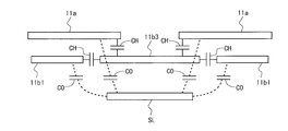
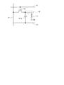
- FIG. 1 is an equivalent circuit diagram showing a configuration of a typical pixel forming portion (portion for forming one pixel) in the display device of the present invention.
- the pixel formation portion includes three thin film transistors T1, T2, and T3 and three capacitors Clc1, Clc2, and Ctr.
- the gate bus line GL and the source bus line SL as a wiring passing through the pixel formation portion, a wiring indicated by a symbol RST (hereinafter referred to as “reset wiring”) and a wiring indicated by a symbol CTL (hereinafter referred to as “control”). Wiring ”) is provided.
- the capacitor Clc1 is referred to as a “first first capacitor”
- the capacitor Clc2 is referred to as a “second first capacitor”
- the capacitor Ctr is referred to as a “second capacitor”.
- the first first capacitor Clc1, the second first capacitor Clc2, and the second capacitor Ctr the capacitance values thereof are also indicated by the same symbols “Clc1”, “Clc2”, and “Ctr”, respectively.
- the control wiring CTL is shown to extend in parallel to the gate bus line GL, but the present invention is not limited to this.
- the pixel formation portion shown in FIG. 1 forms a pixel having a multi-pixel structure. That is, one pixel is divided into a plurality of subpixels (here, two subpixels).
- the first first capacitor Clc1 is a capacitor provided in a pixel in which a relatively dark display (hereinafter referred to as “dark display”) is performed
- the second first capacitor Clc2 is relatively
- the first first capacitor Clc1 may be a capacitor provided in a pixel for bright display
- the second first capacitor Clc2 may be a capacitor provided in a pixel for dark display.
- connection relationship between the components in the pixel forming section is as follows.
- the gate electrode is connected to the gate bus line GL
- the source electrode is connected to the source bus line SL
- the drain electrode is connected to one end of the first first capacitor Clc1 and one end of the second capacitor Ctr.
- the gate electrode is connected to the reset wiring RST
- the source electrode is connected to the source bus line SL
- the drain electrode is connected to the other end of the second capacitor Ctr and one end of the second first capacitor Clc2. Yes.
- the gate electrode is connected to the reset wiring RST, the source electrode is connected to the control wiring CTL, and the drain electrode is connected to one end of the second capacitor Ctr.
- One end of the first first capacitor Clc1 is connected to the drain electrode of the thin film transistor T1 and one end of the second capacitor Ctr, and the other end of the first first capacitor Clc1 is connected to the common electrode COM.
- One end of the second first capacitor Clc2 is connected to the drain electrode of the thin film transistor T2 and the other end of the second capacitor Ctr, and the other end of the second first capacitor Clc2 is connected to the common electrode COM.
- One end of the second capacitor Ctr is connected to the drain electrode of the thin film transistor T1, the drain electrode of the thin film transistor T3, and one end of the first first capacitor Clc1, and the other end of the second capacitor Ctr is connected to the drain electrode of the thin film transistor T2 and the second electrode. It is connected to one end of the first capacitor Clc2.
- the first first capacitor Clc1 and the second first capacitor Clc2 correspond to the liquid crystal capacitor.
- the pixel electrode 1011 for dark display exists at one end of the first first capacitor Clc1. That is, the first capacitor Clc1 is formed by the pixel electrode 1011 for dark display and the common electrode COM.
- a pixel electrode 1012 for bright display exists at one end of the second first capacitor Clc2. That is, the second first capacitor Clc2 is formed by the pixel electrode 1012 for bright display and the common electrode COM.
- one end of the second capacitor Ctr has a capacitor (bright display pixel electrode 1012) between the pixel electrode 1012 for bright display or an electrode electrically connected to the pixel electrode 1012 for bright display.
- an electrode (hereinafter referred to as an “amplifying electrode”) 102 for forming a capacitor for amplifying the potential of the first electrode 102. Since the amplification electrode 102 is electrically connected to the pixel electrode 1011 for dark display, the potential of the amplification electrode 102 is equal to the potential of the pixel electrode 1011 for dark display.
- the potential of the pixel electrode 1011 for dark display (the potential of the amplification electrode 102) is represented by a symbol Vpix1
- the potential of the pixel electrode 1012 for bright display is represented by a symbol Vpix2.
- the first switching element is realized by the thin film transistor T1
- the second switching element is realized by the thin film transistor T2
- the third switching element is realized by the thin film transistor T3, and the first switching element is realized by the control wiring CTL.
- the control wiring is realized
- the second control wiring is realized by the reset wiring RST
- the first pixel electrode is realized by the pixel electrode 1011 for dark display
- the second pixel electrode is realized by the pixel electrode 1012 for bright display.
- the gate electrode corresponds to the control terminal
- the source electrode corresponds to the first conduction terminal
- the drain electrode corresponds to the second conduction terminal.
- the amplification circuit unit 13 for amplifying the pixel electrode potential Vpix2 is realized by the thin film transistor T2, the thin film transistor T3, and the second capacitor Ctr.
- FIG. 2 shows the operation of the pixel formation section in the selection period (period for writing to the first first capacitor Clc1 and the second first capacitor Clc2 in accordance with the image to be displayed in each pixel formation section). It is a signal waveform diagram for explaining.
- the length of the selection period typically corresponds to the length of one horizontal scanning period in a conventional display device.
- the symbol Vdata represents the video signal potential (the potential of the source bus line SL)
- the symbol Vctl represents the potential of the control wiring CTL.
- the selection period horizontal scanning period
- the selection period is the first half period (hereinafter referred to as “precharge period”) Ta and the second half period (hereinafter referred to as “amplification period”).
- Tb the first half period
- amplification period the second half period
- one frame period includes a selection period including the precharge period Ta and the amplification period Tb, and a non-selection period that is a period other than the selection period.
- the length of the precharge period Ta and the length of the amplification period Tb are not necessarily equal. Note that since the same operation is performed for a frame in which positive polarity writing is performed and a frame in which negative polarity writing is performed, the following description will be focused on a frame in which positive polarity writing is performed.
- the gate line GL is supplied with an off-level (low level in the example shown in FIG. 2) potential, and the reset wiring RST is on-level (high level in the example shown in FIG. 2). ) Potential.
- the thin film transistor T1 is turned off and the thin film transistors T2 and T3 are turned on.
- the video signal potential Vdata is applied to the pixel electrode 1012 for bright display
- the control wiring potential Vctl is applied to the pixel electrode 1011 for dark display (amplification electrode 102).
- the video signal potential Vdata is a potential determined according to the display image.
- an on-level potential is applied to the gate bus line GL while an off-level potential is applied to the reset wiring RST.
- the thin film transistor T1 is turned on and the thin film transistors T2 and T3 are turned off.
- the video signal potential Vdata is applied to the pixel electrode 1011 for dark display. That is, the pixel electrode potential Vpix1 rises from Vctl to Vdata.
- the pixel electrode potential Vpix2 rises via the second capacitor Ctr as the pixel electrode potential Vpix1 rises.
- the magnitude V1 of the increase in the pixel electrode potential Vpix2 at this time is expressed by the following equation (1).
- Cp represents the capacitance value of the parasitic capacitance.
- the value of the pixel electrode potential Vpix1 is Vdata
- the value of the pixel electrode potential Vpix2 is “Vdata + V1”.
- the potential of the gate bus line GL changes from the on level to the off level.
- voltage fluctuations ⁇ Vg1, ⁇ Vg2 called “feedthrough voltage”, “pull-in voltage”, etc. occur in the pixel electrode potentials Vpix1, Vpix2.
- the value of the pixel electrode potential Vpix1 is “Vdata ⁇ Vg1”
- the pixel electrode potential Vpix2 is a value represented by the following equation (2). Note that when the positive polarity writing is performed, the above voltage fluctuation occurs so that the difference between the pixel electrode potential and the common electrode potential is reduced.
- the pixel electrode potential and the common electrode potential are The voltage fluctuation occurs so that the difference becomes large.
- the pixel electrode potential Vpix1 is maintained at “Vdata ⁇ Vg1” and the pixel electrode potential Vpix2 is expressed by the above formula (from the time when the voltage variation occurs to the time when writing is performed in the next frame after the selection period ends. 2) (however, fluctuations in potential due to leakage current or the like are ignored).
- the pixel electrode potential changing step is realized by the operation in the selection period
- the pixel electrode potential maintaining step is realized by the operation in the non-selection period.
- the first step is realized by the operation in the precharge period Ta
- the second step is realized by the operation in the amplification period Tb.
- the pixel electrode potential for dark display is lower than the video signal potential at the end of the selection period, and the pixel electrode potential for bright display is equal to the video signal potential. It was. From this and the above equation (2), according to the display device of the present invention, the pixel electrode potential Vpix2 for bright display at the end of the selection period is (Ctr / (Ctr + Clc2 + Cp)) ⁇ ( It can be seen that it is increased by the magnitude of Vdata ⁇ Vctl). Further, from the above equation (2), it is understood that the pixel electrode potential Vpix2 is amplified according to the magnitude of (Vdata ⁇ Vctl) during the amplification period Tb.
- the above equation (2) can be modified as shown in the following equation (3).
- the video signal potential Vdata is amplified by (1+ (Ctr / (Ctr + Clc2 + Cp)) times as much as the conventional one based on the potential obtained by amplifying the pixel electrode potential Vpix2. It is understood that the value is determined. Further, it is understood that the pixel electrode potential Vpix2 is offset based not only on the voltage fluctuation ⁇ Vg2 but on the value of the control wiring potential Vctl.
- control wiring CTL may be DC driving or AC driving.
- the value of the control wiring potential Vctl and the negative polarity writing when the positive polarity writing is performed are performed according to the above equation (3). It is understood that the degree of amplification of the pixel electrode potential Vpix2 can be changed by setting the value of the control wiring potential Vctl at various times (when the video signal potential Vdata is lower than the common electrode potential).
- FIG. 3 is a diagram showing the relationship between the difference between the video signal potential and the common electrode potential and the transmittance.
- the characteristic representing the relationship between the liquid crystal applied voltage and the transmittance in the liquid crystal display device is referred to as “VT characteristic”. Therefore, the characteristic representing the relationship shown in FIG. 3 is referred to as “pseudo VT characteristic” for convenience.
- the solid line denoted by reference numeral 71 represents the pseudo VT characteristic in the dark display pixel.
- the “difference between the video signal potential and the common electrode potential” necessary for obtaining an arbitrary transmittance is smaller in the bright display pixel than in the dark display pixel. Therefore, according to the display device of the present invention, when the control wiring CTL is DC driven, the pixel for bright display can obtain a pseudo VT characteristic represented by a thick solid line indicated by reference numeral 72, for example. Further, by driving the control wiring CTL with an alternating current, the pseudo VT characteristic of the bright display pixel can be shifted.
- the pixel electrode potential Vpix2 is increased by the amplification period Tb. It is greatly amplified. Thereby, in the pixel for bright display, for example, a pseudo VT characteristic represented by a thick dotted line indicated by reference numeral 73 is obtained.
- the pixel electrode potential Vpix2 in the amplification period Tb is set.
- the degree of amplification is reduced.
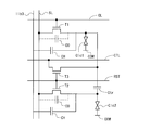
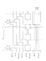
- FIG. 4 is a block diagram showing the overall configuration of the active matrix liquid crystal display device according to the first embodiment of the present invention.
- the liquid crystal display device includes a display unit 100, a display control circuit 200, a gate driver 300, a source driver 400, a reset wiring driver 500, and a control wiring driver 600.
- the display unit 100 is provided corresponding to a plurality of source bus lines SL, a plurality of gate bus lines GL, and intersections of the plurality of source bus lines SL and the plurality of gate bus lines GL. And a plurality of pixel formation portions.
- the display unit 100 includes a reset wiring RST provided to correspond to the gate bus line GL on a one-to-one basis and a control wiring CTL provided to correspond to the gate bus line GL on a one-to-one basis.
- a reset wiring RST provided to correspond to the gate bus line GL on a one-to-one basis
- a control wiring CTL provided to correspond to the gate bus line GL on a one-to-one basis.
- the display control circuit 200 receives the image data DAT and the timing signal group TG, and controls the control signal SG for controlling the operation of the gate driver 300, the control signal SS for controlling the operation of the source driver 400, and the image data DAT.
- a control signal SR for controlling the operation of the reset wiring driver 500, and a control signal SC for controlling the operation of the control wiring driver 600 are output.
- Each control signal is composed of one or a plurality of signals.
- the control signal SG includes a start pulse signal indicating the start timing of the vertical scanning period and a clock signal for controlling the timing of the shift operation in the shift register in the gate driver 300.
- the gate driver 300 drives the gate bus line GL based on the control signal SG.
- the source driver 400 drives the source bus line SL based on the control signal SS.
- the reset wiring driver 500 drives the reset wiring RST based on the control signal SR.
- the control wiring driver 600 drives the control wiring CTL based on the control signal SC.
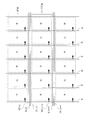
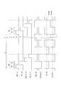
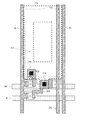
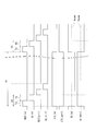
- FIG. 5 is a diagram illustrating an arrangement relationship between the pixel formation portion and each line (source bus line SL, gate bus line GL, reset wiring RST, and control wiring CTL).
- the supply direction of the video signal from the source bus line SL to the pixel formation portion is indicated by an arrow.
- R, G, and B respectively indicate a red pixel formation portion, a green pixel formation portion, and a blue pixel formation portion.
- the video signal is supplied from the source bus line SL arranged on the same side (left side in this example) in all the pixel forming portions.
- a single pixel is divided into a plurality of sub-pixels (here, two sub-pixels including a dark display pixel and a bright display pixel). It has a pixel structure.
- the gate metal forming the gate bus line GL and the source metal forming the source bus line SL are arranged so as to be orthogonal to each other.
- the reset wiring RST and the control wiring CTL are formed of gate metal and are disposed so as to extend in parallel with the gate bus line GL.
- the area other than the area where the reset wiring RST, the gate bus line GL, and the control wiring CTL are arranged is used for dark display.
- the transparent electrode 111 that functions as the pixel electrode 1011 and the transparent electrode 112 that functions as the pixel electrode 1012 for bright display are formed.
- the transparent electrode 111 and the transparent electrode 112 are formed in the same layer.
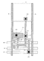
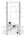
- the electrode 12 functioning as the amplification electrode 102 described above is formed as shown in FIG. 6 by gate metal between two adjacent source bus lines SL.
- the drain electrode of the thin film transistor T1 and the transparent electrode 111 are electrically connected by a source metal indicated by reference numeral SE1 and a contact CT0.
- the drain electrode of the thin film transistor T1 and the electrode 12 are electrically connected by a source metal denoted by reference numeral SE1 and a contact CT1.
- the drain electrode of the thin film transistor T2 and the transparent electrode 112 are electrically connected to each other by a source metal indicated by reference numeral SE2 and a contact CT2.
- the source electrode of the thin film transistor T3 and the control wiring CTL are electrically connected by a source metal indicated by reference numeral SE3 and a contact CT3.
- the drain electrode of the thin film transistor T3 and the electrode 12 are electrically connected by a source metal indicated by reference numeral SE1 and a contact CT1.
- the second capacitor Ctr is formed by the source metal indicated by reference numeral SE2 and the electrode 12.
- FIG. 7 shows the positions of the transparent electrode 111, the transparent electrode 112, the electrode 12, the source metal denoted by reference numerals SE1 to SE3, and the contacts CT0 to CT3 in FIG. 6 on the equivalent circuit diagram shown in FIG. It becomes as follows.
- a driving method in the present embodiment will be described.
- a constant potential is applied to the control wiring CTL throughout the operation of the liquid crystal display device (see also FIG. 5). That is, direct current drive is performed for the control wiring CTL.
- a positive video signal and a negative video signal are alternately applied to the source bus line SL every horizontal scanning period. At any time, video signals having the same polarity are given to all the source bus lines SL.
- a method called “1H line inversion driving” is adopted for the polarity inversion of the pixel.
- any one of “1H line inversion driving”, “dot inversion driving”, and “column inversion driving” can be applied to the polarity inversion of the pixel. good.
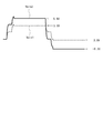
- FIG. 9 is a signal waveform diagram for explaining the operation of the pixel formation portion in the selection period in the present embodiment.
- the selection period is composed of the precharge period Ta and the amplification period Tb.
- the control wiring potential Vctl is set to a value lower than the common electrode potential Vcom.
- an on-level potential is applied to the reset wiring RST while an off-level potential is applied to the gate bus line GL.
- the thin film transistor T1 is turned off and the thin film transistors T2 and T3 are turned on.
- the video signal potential Vdata is applied to the transparent electrode 112 that functions as the pixel electrode 1012 for bright display
- the control wiring potential Vctl is applied to the transparent electrode 111 that functions as the pixel electrode 1011 for dark display.
- an on-level potential is applied to the gate bus line GL while an off-level potential is applied to the reset wiring RST.
- the thin film transistor T1 is turned on and the thin film transistors T2 and T3 are turned off.
- the pixel electrode potential Vpix1 rises from Vctl to Vdata.
- the pixel electrode potential Vpix2 increases by the magnitude V1 shown in the above equation (1).
- the pixel electrode potential Vpix1 decreases by ⁇ Vg1
- the pixel electrode potential Vpix2 decreases by ⁇ Vg2.
- the value of the pixel electrode potential Vpix1 is “Vdata ⁇ Vg1”
- the pixel electrode potential Vpix2 is a value represented by the above equation (2).
- voltages having different magnitudes are applied to the liquid crystal between the dark display pixels and the bright display pixels, and the viewing angle characteristics are improved.
- movement of the odd frame was demonstrated here, the same operation
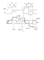
- ⁇ Vg1 and ⁇ Vg2 have different sizes due to the configuration of the pixel circuit. For this reason, if the control wiring potential Vctl is not set to a suitable value, the counter adjustment (the common electrode potential Vcom is set in consideration of the voltage fluctuation) is performed even if the pixel for dark display is used as a reference. Even in a bright display pixel, the liquid crystal applied voltage when positive polarity writing is performed differs from the liquid crystal applied voltage when negative polarity writing is performed. For example, as shown in FIG.
- Vpix1 Vd1 ⁇ Vg1” is obtained when writing in the positive polarity
- their median values should be set as the value of the common electrode potential Vcom. Therefore, if the median value of the video signal potential Vdata is 0V, the value of the common electrode potential Vcom is preferably set to ⁇ Vg1.
- the value of the common electrode potential Vcom is set to a potential that is lower than the reference potential by ⁇ Vg1. It is preferred that
- the median value of the pixel electrode potential Vpix2 at the time of positive polarity writing and the pixel electrode potential Vpix2 at the time of negative polarity writing is set as described above. It is necessary to be equal to the value of the common electrode potential Vcom set as described above.
- Vctl ⁇ Vg1 ⁇ Vg2 (6)
- the voltage fluctuations ⁇ Vg1, ⁇ Vg2, etc. are set so that the median value of the pixel electrode potential Vpix2 at the time of positive writing and the pixel electrode potential Vpix2 at the time of negative writing matches the common electrode potential Vcom. Based on this, it is preferable that the value of the control wiring potential Vctl is set.
- the median value of the video signal potential Vdata is 0V
- the voltage fluctuation ⁇ Vg1 is 0.1V
- the voltage fluctuation ⁇ Vg2 is 0.3V.
- the common electrode potential Vcom is set to -0.1V
- the control wiring potential Vctl is set to -0.2V.
- the pixel electrode potential Vpix1 is ⁇ 0.2V and the pixel electrode potential Vpix2 is 3.0V during the precharge period Ta.
- the pixel electrode potential Vpix1 rises from ⁇ 0.2V to 3.0V.
- the pixel electrode potential Vpix2 rises from 3.0V to 6.2V.
- the pixel electrode potential Vpix1 decreases from 3.0 V to 2.9 V due to the voltage variation ⁇ Vg1
- the pixel electrode potential Vpix2 decreases from 6.2 V to 5.9 V due to the voltage variation ⁇ Vg2.
- the pixel electrode potential Vpix1 is ⁇ 0.2V
- the pixel electrode potential Vpix2 is ⁇ 3.0V.
- the pixel electrode potential Vpix1 decreases from ⁇ 0.2V to ⁇ 3.0V.
- the pixel electrode potential Vpix2 decreases from ⁇ 3.0V to ⁇ 5.8V.
- the pixel electrode potential Vpix1 decreases from ⁇ 3.0V to ⁇ 3.1V due to the voltage variation ⁇ Vg1
- the pixel electrode potential Vpix2 decreases from ⁇ 5.8V to ⁇ 6.1V due to the voltage variation ⁇ Vg2. .
- a potential of ⁇ 3.1 V to 2.9 V is applied to the pixel electrode 1011 for dark display, and a potential of ⁇ 6.1 V to 5.9 V is applied to the pixel electrode 1012 for bright display. Is given.
- the liquid crystal applied voltage is not biased between the positive and negative polarities.
- the pixel electrode potential Vpix2 for bright display is made equal to the video signal potential Vdata during the precharge period Ta, and then according to the difference between the video signal potential Vdata and the control wiring potential Vctl during the amplification period Tb. Amplified. Accordingly, at the end of the selection period, the pixel electrode potential Vpix1 for dark display becomes equal to the video signal potential Vdata, and the pixel electrode potential Vpix2 for bright display becomes higher than the video signal potential Vdata.
- the pixel electrode potential for dark display is lower than the video signal potential at the end of the selection period.
- the pixel electrode potential for display was equal to the video signal potential.
- the amplitude of the video signal is made smaller than before, it is possible to perform the same image display as before.
- the amplitude of the video signal can be made smaller than before, the power consumption is reduced more than before.
- the common electrode potential Vcom and the control wiring potential Vctl are set to appropriate values, liquid crystal application between positive and negative polarities is performed in both the dark display pixel and the bright display pixel. Occurrence of voltage bias is suppressed, and deterioration of liquid crystal reliability (such as occurrence of image sticking to the screen) is suppressed.
- control wiring CTL is disposed so as to extend in parallel with the gate bus line GL.
- the number of gate bus lines GL is smaller than the number of source bus lines SL, so that it is necessary as compared with a configuration in which the control wiring CTL is arranged to extend in parallel to the source bus lines SL.
- the number of control wirings CTL is reduced. For this reason, it is possible to suppress a decrease in the aperture ratio due to the provision of the control wiring CTL.
- Second Embodiment> ⁇ 2.1 Configuration> The configuration of the pixel formation unit, the overall configuration, the arrangement relationship between the pixel formation unit and each line, and the layout in the vicinity of the pixel formation unit are the same as those in the first embodiment, and thus description thereof is omitted (FIGS. 1 and 4). FIG. 5 and FIG. 6). In the present embodiment, which of the pixel electrode 1011 and the pixel electrode 1012 becomes the pixel electrode for bright display is determined according to the value of the control wiring potential Vctl.
- a constant high level potential and a constant low level potential are alternately applied to the control wiring CTL every frame (one vertical scanning period). That is, AC driving is performed for the control wiring CTL.
- a positive video signal and a negative video signal are alternately applied to the source bus line SL every horizontal scanning period. At any time, video signals having the same polarity are given to all the source bus lines SL.
- a method called “1H line inversion driving” is adopted for the polarity inversion of the pixel.
- FIG. 13 is a signal waveform diagram for explaining the operation of the pixel formation portion in the selection period in the present embodiment.
- the control wiring potential Vctl is negative.
- the control wiring potential Vctl is positive.
- the video signal potential Vdata varies between ⁇ 3.0 V and 3.0 V
- the control wiring potential Vctl when the positive writing is performed is
- the control wiring potential Vctl is set to ⁇ 2.0 V and the negative voltage writing is performed
- the control wiring potential Vctl is set to 1.6 V
- the voltage fluctuation ⁇ Vg1 becomes 0.1 V
- the voltage fluctuation ⁇ Vg2 becomes 0.3 V.
- the operation of the pixel formation portion in the selection period is as follows (see FIG. 14).
- the pixel electrode potential Vpix1 is ⁇ 2.0V and the pixel electrode potential Vpix2 is 3.0V during the precharge period Ta.
- the pixel electrode potential Vpix1 rises from ⁇ 2.0V to 3.0V.
- the pixel electrode potential Vpix2 rises from 3.0V to 8.0V.
- the pixel electrode potential Vpix1 decreases from 3.0 V to 2.9 V due to the voltage variation ⁇ Vg1
- the pixel electrode potential Vpix2 decreases from 8.0 V to 7.7 V due to the voltage variation ⁇ Vg2.
- the pixel electrode potential Vpix1 is 1.6V and the pixel electrode potential Vpix2 is ⁇ 3.0V in the precharge period Ta.
- the pixel electrode potential Vpix1 decreases from 1.6V to ⁇ 3.0V.
- the pixel electrode potential Vpix2 decreases from ⁇ 3.0V to ⁇ 7.6V.
- the pixel electrode potential Vpix1 decreases from ⁇ 3.0V to ⁇ 3.1V due to the voltage variation ⁇ Vg1
- the pixel electrode potential Vpix decreases from ⁇ 7.6V to ⁇ 7.9V due to the voltage variation ⁇ Vg.
- the pixel electrode 1011 is supplied with a potential of ⁇ 3.1 V to 2.9 V
- the pixel electrode 1012 is supplied with a potential of ⁇ 7.9 V to 7.7 V.
- the amplitude of the pixel electrode potential Vpix2 is larger than that of the example shown in the first embodiment (see FIG. 11).
- the above-described pseudo VT characteristic for the pixel including the pixel electrode 1012 is shifted in the minus direction (left direction in FIG. 3).
- a pseudo VT characteristic represented by a solid line 71 is obtained for one subpixel
- a pseudo VT characteristic represented by a thick dotted line 73 is obtained for the other subpixel. Is obtained "(see FIG. 3).
- the larger the difference between the video signal potential and the common electrode potential the greater the difference in transmittance between the two sub-pixels.
- the video signal potential Vdata varies between ⁇ 3.0 V and 3.0 V
- the control wiring potential when positive writing is performed When Vctl is set to 5.0 V, the control wiring potential Vctl when negative polarity writing is performed is set to ⁇ 5.4 V, the voltage fluctuation ⁇ Vg 1 becomes 0.1 V, and the voltage fluctuation ⁇ Vg 2 becomes 0.3 V.
- the operation of the pixel formation portion in the selection period is as follows (see FIG. 15).
- the pixel electrode potential Vpix1 is 5.0V
- the pixel electrode potential Vpix2 is 3.0V.
- the pixel electrode potential Vpix1 decreases from 5.0V to 3.0V.
- the pixel electrode potential Vpix2 decreases from 3.0V to 1.0V.
- the pixel electrode potential Vpix1 decreases from 3.0 V to 2.9 V due to the voltage variation ⁇ Vg1
- the pixel electrode potential Vpix2 decreases from 1.0 V to 0.7 V due to the voltage variation ⁇ Vg2.
- the pixel electrode potential Vpix1 is ⁇ 5.4V and the pixel electrode potential Vpix2 is ⁇ 3.0V in the precharge period Ta.
- the pixel electrode potential Vpix1 rises from ⁇ 5.4V to ⁇ 3.0V. Accordingly, the pixel electrode potential Vpix2 increases from ⁇ 3.0V to ⁇ 0.6V.
- the pixel electrode potential Vpix1 decreases from ⁇ 3.0V to ⁇ 3.1V due to the voltage variation ⁇ Vg1
- the pixel electrode potential Vpix decreases from ⁇ 0.6V to ⁇ 0.9V due to the voltage variation ⁇ Vg.
- the pixel electrode 1011 is supplied with a potential from ⁇ 3.1 V to 2.9 V
- the pixel electrode 1012 is supplied with a potential from ⁇ 0.9 V to 0.7 V.
- the amplitude of the pixel electrode potential Vpix2 is smaller than the example shown in the first embodiment (see FIG. 11).
- the above-described pseudo VT characteristic for the pixel including the pixel electrode 1012 is shifted in the plus direction (right direction in FIG. 3).
- a pseudo VT characteristic represented by a solid line 71 is obtained for one subpixel
- a pseudo VT characteristic represented by a thick dashed line 74 for the other subpixel.
- the degree of amplification of the pixel electrode potential Vpix2 can be changed by setting the value of the control wiring potential Vctl to various values. This makes it possible to shift the above-described pseudo VT characteristic for one subpixel in a wide range, and the degree of freedom in viewing angle compensation is improved. Further, since the control wiring CTL is arranged so as to extend in parallel with the gate bus line GL, a decrease in the aperture ratio due to the provision of the control wiring CTL can be suppressed as in the first embodiment.
- FIG. 16 is a diagram illustrating a layout in the vicinity of the pixel formation portion in the first modification.
- the control wiring CTL is arranged to extend in parallel with the gate bus line GL (see FIG. 6).
- the control wiring CTL extends in parallel to the source bus line SL. It is arranged. Therefore, in the present modification, the control wiring CTL intersects with the gate bus line GL. For this reason, the control wiring CTL is formed not by the gate metal but by the source metal.
- the arrangement relationship between the pixel formation portion and each line is as shown in FIG. 17, for example.
- FIG. 18 is a signal waveform diagram for explaining the driving method in the present modification (see also FIG. 17).
- a constant high level potential and a constant low level potential are alternately applied to the control wiring every horizontal scanning period. That is, AC driving is performed for the control wiring.
- two adjacent control wirings (for example, CTL (m) and CTL (m + 1)) are given different levels of potential.
- a positive video signal and a negative video signal are alternately supplied to the source bus line every horizontal scanning period (see FIG. 8).
- video signals having different polarities are applied to two adjacent source bus lines (for example, SL (m) and SL (m + 1)).
- each control wiring CTL is connected to a number of thin film transistors T3 equal to the number of source bus lines SL, and all the thin film transistors T3 connected to one control wiring CTL are connected to the control wiring CTL.
- a precharge potential is applied from CTL at the same timing.
- the precharge potential is not applied from the single control wiring CTL to the plurality of thin film transistors T3 at the same timing. Therefore, according to this modification, it is possible to reduce a load applied to one control wiring CTL when precharging is performed.
- FIG. 19 is a diagram showing a layout in the vicinity of the pixel formation portion in the second modification.
- the transparent electrode has one layer (see FIG. 6), but in the present modification, the transparent electrode has two layers.
- the pixel electrode 1011 for dark display is formed in a portion other than the region where the reset wiring RST, the gate bus line GL, and the control wiring CTL are arranged in a region between two adjacent source bus lines SL.
- a functioning upper transparent electrode (first transparent electrode) 11a and a lower transparent electrode (second transparent electrode) 11b functioning as a pixel electrode 1012 for bright display are provided.
- Two capacitors Ctr are formed.
- the shapes of the upper transparent electrode 11a and the lower transparent electrode 11b are as shown in FIG.
- the drain electrode of the thin film transistor T1 and the upper transparent electrode 11a are electrically connected by a source metal indicated by reference numeral SE4 and a contact CT4.
- the drain electrode of the thin film transistor T2 and the lower transparent electrode 11b are electrically connected by a source metal indicated by reference numeral SE5 and a contact CT5.
- the source electrode of the thin film transistor T3 and the control wiring CTL are electrically connected by a source metal indicated by reference numeral SE6 and a contact CT6.
- the drain electrode of the thin film transistor T3 and the upper transparent electrode 11a are electrically connected by a source metal indicated by reference numeral SE4 and a contact CT4.
- FIG. 21 is a cross-sectional view taken along line AA in FIG.
- the upper transparent electrode 11a is arranged closer to the common electrode COM than the lower transparent electrode 11b.
- an opening is provided in the center of the upper transparent electrode 11a.
- the second capacitor is formed by two transparent electrodes.
- the aperture ratio can be increased as compared with the above embodiments (see FIG. 6), and the second capacitance is set without affecting the aperture ratio (since the electrode is transparent).
- the control wiring CTL is arranged so as to extend in parallel with the gate bus line GL, a decrease in the aperture ratio due to the provision of the control wiring CTL is suppressed as in the above embodiments.
- the upper transparent electrode 11a functions as the pixel electrode 1011 for dark display and the lower transparent electrode 11b functions as the pixel electrode 1012 for bright display has been described, but this relationship is reversed. May be. Further, regarding the upper transparent electrode 11a, in FIG. 20 and FIG. 21, an opening is provided at the center, but an electrode having a shape shown as an opening in FIG. 20 may be used as the upper transparent electrode 11a. However, in consideration of the alignment characteristics of the liquid crystal, it is preferable that a sub-pixel for bright display is arranged at the center of each pixel.
- FIG. 22 is a diagram illustrating a layout in the vicinity of the pixel formation portion in the third modification. Similar to the first modification, the control wiring CTL is arranged to extend in parallel with the source bus line SL. Further, as in the second modification, the transparent electrode has two layers. Note that the source electrode of the thin film transistor T3 and the control wiring CTL are directly connected as shown in FIG. With the configuration as described above, as in the first modification, a precharge potential is not applied from one control wiring CTL to a plurality of thin film transistors T3 at the same timing. It is possible to reduce the load applied to the control wiring CTL. As in the second modification, the aperture ratio can be increased as compared with the above embodiments, and the second capacity is set without affecting the aperture ratio.
- FIG. 23 is a diagram illustrating a layout in the vicinity of the pixel formation portion in the fourth modification.
- the upper transparent electrode 11a has the same shape as that of the second modification.
- the lower transparent electrode is divided into two parts denoted by reference numerals 11b1 and 11b2 in FIG. 24 in this modification.
- One lower transparent electrode 11b1 functions as a pixel electrode 1012 for bright display, and the other lower transparent electrode 11b2 functions as a control wiring CTL.
- the lower transparent electrode 11b2 having a shape as shown in FIG.
- the control wiring CTL is provided in a lattice shape in the display unit 100.
- the source electrode of the thin film transistor T3 and the control wiring CTL are electrically connected by a source metal indicated by reference numeral SE7 and a contact CT7.
- SE7 source metal indicated by reference numeral SE7
- a contact CT7 a source metal indicated by reference numeral SE7 and a contact CT7.
- the arrangement relationship between the pixel forming portion and each line is as shown in FIG. 25, for example.
- lattice-like electrode part is implement
- FIG. 26 is a signal waveform diagram for explaining the driving method in the present modification (see also FIG. 25).
- a constant high level potential and a constant low level potential are alternately applied to the control wiring CTL every horizontal scanning period. That is, AC driving is performed for the control wiring CTL.
- a positive video signal and a negative video signal are alternately applied to the source bus line SL every horizontal scanning period. At any time, video signals having the same polarity are given to all the source bus lines SL.
- a method called “1H line inversion driving” is adopted for the polarity inversion of the pixels. Note that in FIG.
- the control wiring CTL is formed by a transparent electrode. For this reason, the aperture ratio can be improved. Further, since the control wiring CTL is provided in a lattice shape in the display unit 100, the resistance of the control wiring CTL is reduced. Although an example in which the control wiring CTL is AC driven is described here, the control wiring CTL may be DC driven as shown in FIG.
- a fifth modification and a sixth modification described below are liquid crystal display devices (hereinafter referred to as “alignment division type”) including pixels composed of a plurality of regions having different alignment states (inclination directions of liquid crystal molecules) of liquid crystals. Applied to a liquid crystal display device).
- the fifth modification will be described in comparison with the second modification (see FIG. 19), and the sixth modification will be described in comparison with the third modification (see FIG. 22).
- FIG. 27 is a diagram showing a layout in the vicinity of the pixel formation portion in the fifth modification.
- the control wiring CTL is disposed so as not to overlap the transparent electrode in the vertical direction.
- the control wiring CTL is disposed so as to overlap the transparent electrode in the vertical direction.
- the dark line 15 is generated at the boundary of the region in the display unit 100, and the control wiring CTL is overlapped with the dark line 15 generated so as to extend parallel to the gate bus line GL. It is made of gate metal.
- the source electrode of the thin film transistor T3 and the control wiring CTL are electrically connected by the source metal indicated by reference numeral SE8 and the contact CT8.
- control wiring CTL is formed so as to overlap the dark line 15 in the alignment-divided liquid crystal display device, so that the reduction in the aperture ratio due to the provision of the control wiring CTL is effectively suppressed.
- the control wiring CTL may be formed so as to overlap the dark line 15 generated so as to extend parallel to the gate bus line GL. it can.
- the sub-pixel for bright display is arranged at the center of each pixel forming portion.
- suitable display in consideration of the alignment characteristics of the liquid crystal is performed.
- the alignment centers of the bright display sub-pixel and the dark display sub-pixel coincide with each other.
- the alignment centers of the bright display sub-pixel and the dark display sub-pixel coincide with each other, so that the number of dark lines can be reduced, and a decrease in transmittance due to the dark lines is suppressed.
- the transparent electrode is composed of one layer (see FIG. 6), since dark lines are generated in both the vertical direction and the horizontal direction in both of the two transparent electrodes, the transmittance decreases.
- FIG. 28 is a diagram showing a layout in the vicinity of the pixel formation portion in the sixth modification.
- the control wiring CTL is arranged so as to overlap the end portion of the lower transparent electrode 11b in the vertical direction.
- the control wiring CTL is disposed so as to overlap the central portion of the lower transparent electrode 11b in the vertical direction.
- the control wiring CTL is formed of a source metal so as to overlap the dark line 15 generated so as to extend in parallel with the source bus line SL.
- the drain electrode of the thin film transistor T1 and the upper transparent electrode 11a are electrically connected by the source metal indicated by reference numeral SE9 and the contact CT9.
- the drain electrode of the thin film transistor T3 and the upper transparent electrode 11a are electrically connected by a source metal indicated by reference numeral SE10 and a contact CT10.
- the control wiring CTL is formed so as to overlap the dark line 15, so that the aperture ratio is reduced by providing the control wiring CTL. Effectively suppressed.
- the control wiring CTL may be formed so as to overlap the dark line 15 generated so as to extend in parallel with the source bus line SL. it can.
- FIG. 29 is a diagram showing a layout in the vicinity of the pixel formation portion in the seventh modification.
- the lower transparent electrode is a parasitic capacitance formed between the portion 11b1 functioning as the pixel electrode 1012 for bright display, and the transparent electrode (upper transparent electrode and lower transparent electrode) and the source bus line SL.
- the transparent electrode upper transparent electrode and lower transparent electrode
- the configuration of this modification is a configuration in which the shield electrode portion 11b3 is added to the configuration of the second modification (see FIG. 19).
- the common electrode potential Vcom is applied to the shield electrode portion 11b3.
- FIG. 30 is a cross-sectional view taken along line AA in FIG. FIG. 30 also shows the upper transparent electrode and the lower transparent electrode in the pixel formation portion on the right side of the pixel formation portion shown in FIG.
- the shield electrode portion 11b3 is formed in a region between the source bus line SL and the upper transparent electrode 11a. By providing the shield electrode portion 11b3 in this way, the parasitic capacitance C0 between the source bus line and the transparent electrode (transparent electrode excluding the shield electrode portion) is reduced. In this modification, the shield electrode portion 11b3 is formed so as to cover the source bus line SL.
- FIG. 31 is an equivalent circuit diagram including the parasitic capacitance C0 between the source bus line and the transparent electrode and the capacitance CH formed between the shield electrode portion and the transparent electrode.
- the capacitance CH formed between the shield electrode portion and the transparent electrode functions as an auxiliary capacitance, and the fluctuation of the video signal potential (the potential of the source bus line SL) is changed to the pixel electrode potentials Vpix1 and Vpix2. It is possible to effectively reduce the influence exerted.
- FIG. 32 is a diagram showing a layout in the vicinity of the pixel formation portion in the eighth modification.
- 33 is a cross-sectional view taken along line AA in FIG.
- the shield electrode portion 11b3 is formed so as to cover the source bus line SL.
- the shield electrode portion is positioned so as to be adjacent to the source bus line SL in plan view. 11b3 is formed.
- the source bus line SL and the lower transparent electrode the portion functioning as the bright display pixel electrode 1012
- 11b1 in the extending direction of the gate bus line GL so as not to overlap the source bus line SL.
- a shield electrode portion 11b3 is formed in the region.
- the capacitance formed between the source bus line SL and the shield electrode portion 11b3 is reduced as compared with the seventh modification. For this reason, the same effect as the seventh modification can be obtained, and the wiring capacity of the source bus line SL can be reduced.
- FIG. 34 is a diagram showing a layout in the vicinity of the pixel formation portion in the ninth modification.
- the shield electrode portion 11b3 in the seventh modification (see FIG. 29) is configured to function also as the control wiring CTL. Therefore, unlike the seventh modification, the control wiring CTL extending in parallel with the gate bus line GL is not provided.
- the source electrode of the thin film transistor T3 and the shield electrode portion 11b3 (control wiring CTL) are electrically connected by the source metal indicated by reference numeral SE11 and the contact CT11.
- FIG. 36 is a signal waveform diagram for describing a driving method in the tenth modification.
- the arrangement relationship between the pixel formation portion and each line is as shown in FIG. 17, for example.
- a constant high level potential and a constant low level potential are alternately applied to the control wiring every frame (one vertical scanning period). That is, AC driving is performed for the control wiring CTL.
- two adjacent control wirings (for example, CTL (m) and CTL (m + 1)) are given different levels of potential.
- a positive video signal and a negative video signal are alternately supplied to the source bus line every frame (one vertical scanning period).
- video signals having different polarities are applied to two adjacent source bus lines (for example, SL (m) and SL (m + 1)).
- a method referred to as “column inversion driving (column inversion driving)” can also be adopted for polarity inversion of pixels.
- the layout near the pixel formation portion is configured as in the first modification (see FIG. 16), the third modification (see FIG. 22), or the sixth modification (see FIG. 28).
- the driving method of this modification can be employed.
- FIG. 37 is a signal waveform diagram for describing a driving method in the eleventh modification.
- the arrangement relationship between the pixel formation portion and each line is as shown in FIG. 38, for example.
- FIG. 38 when attention is paid to one source bus line, pixel formation portions that receive video signals from the source bus line are arranged in a staggered manner on both sides of the source bus line.
- the source bus line is driven as in the tenth modification.
- a constant high level potential and a constant low level potential are alternately applied to the control wiring every horizontal scanning period. That is, AC driving is performed for the control wiring.
- two adjacent control wirings for example, CTL (m) and CTL (m + 1) are given different levels of potential.
- the layout near the pixel formation portion is configured as in the first modification (see FIG. 16), the third modification (see FIG. 22), or the sixth modification (see FIG. 28).
- the driving method of this modification can be employed.
- the source bus lines are driven in the same manner as the column inversion drive, but the occurrence of flicker is suppressed because the pixel forming portions connected to the source bus lines are arranged in a staggered manner. .
- dot inversion driving is employed for pixel polarity inversion (see FIG. 18).
- the layout in the vicinity of the pixel formation portion is configured as in the third modification (see FIG. 22) or the sixth modification (see FIG. 28), and the control wiring CTL is AC driven, Similarly, dot inversion driving can be employed.
- FIG. 39 is an equivalent circuit diagram showing the configuration of the pixel formation portion in this modification.
- the amplifier circuit unit 13 includes two amplification stages (a first amplification stage 131 and a second amplification stage 132).
- the first amplification stage 131 includes a thin film transistor T21, a thin film transistor T31, and a first second capacitor Ctr1.
- the second amplification stage 132 includes a thin film transistor T22, a thin film transistor T32, a second second capacitor Ctr2, and a first first capacitor Clc1.
- reset lines RST1 and RST2 and control lines CTL1 and CTL2 are provided as lines that pass through the pixel formation portion.
- the pixel formation portion includes a thin film transistor T1 and a second first capacitor Clc2.
- the pixel electrode 1011 for dark display exists at one end of the first first capacitor Clc1. That is, the first capacitor Clc1 is formed by the pixel electrode 1011 for dark display and the common electrode COM.
- a pixel electrode 1012 for bright display exists at one end of the second first capacitor Clc2. That is, the second first capacitor Clc2 is formed by the pixel electrode 1012 for bright display and the common electrode COM.
- one end of the first second capacitor Ctr1 has a capacitance (bright display pixel electrode) between the pixel electrode 1012 for bright display or an electrode electrically connected to the pixel electrode 1012 for bright display.
- first amplification electrode for forming a capacitor for amplifying the potential of the pixel electrode 1012. Since the first amplification electrode 1021 is electrically connected to the dark display pixel electrode 1011, the potential of the first amplification electrode 1021 is equal to the potential of the dark display pixel electrode 1011. Furthermore, one end of the second second capacitor Ctr2 has a capacitor (dark display) between the pixel electrode 1011 for dark display or an electrode electrically connected to the pixel electrode 1011 for dark display. There is an electrode (hereinafter referred to as “second amplification electrode”) 1022 for forming a capacitor for amplifying the potential of the pixel electrode 1011.
- the potential of the second amplification electrode 1022 is represented by the symbol Vpix1
- the potential of the pixel electrode 1011 for dark display is represented by the symbol Vpix2.
- the potential of the pixel electrode 1012 for bright display is represented by reference numeral Vpix3.
- the connection relationship between the components in the pixel forming section is as follows.
- the gate electrode is connected to the gate bus line GL
- the source electrode is connected to the source bus line SL
- the drain electrode is connected to one end of the second second capacitor Ctr2.
- the gate electrode is connected to the reset wiring RST2
- the source electrode is connected to the source bus line SL
- the drain electrode is connected to one end of the first first capacitor Clc1 and the other end of the second second capacitor Ctr2. It is connected.
- the gate electrode is connected to the reset wiring RST2
- the source electrode is connected to the control wiring CTL2
- the drain electrode is connected to one end of the second second capacitor Ctr2.
- the other end of the second second capacitor Ctr2, the drain electrode of the thin film transistor T22, and one end of the first first capacitor Clc1 are connected to one end of the first second capacitor Ctr1 and the drain electrode of the thin film transistor T31.
- the other end of the first first capacitor Clc1 is connected to the common electrode COM.
- the gate electrode is connected to the reset wiring RST1
- the source electrode is connected to the source bus line SL
- the drain electrode is connected to the other end of the first second capacitor Ctr1.
- the gate electrode is connected to the reset wiring RST1
- the source electrode is connected to the control wiring CTL1
- the drain electrode is connected to one end of the first second capacitor Ctr1.
- One end of the second first capacitor Clc2 is connected to the drain electrode of the thin film transistor T21 and the other end of the first second capacitor Ctr1, and the other end of the second first capacitor Clc2 is connected to the common electrode COM.
- FIG. 40 is a signal waveform diagram for explaining the operation of the pixel formation portion in the selection period in the present modification.
- the selection period includes a precharge period Ta, a first amplification period Tb1, and a second amplification period Tb2.
- an on-level potential is applied to the reset wiring RST1 while an off-level potential is applied to the gate bus line GL and the reset wiring RST2.
- the thin film transistors T1, T22, and T32 are turned off and the thin film transistors T21, T31 are turned on.
- the video signal potential Vdata is applied to the pixel electrode 1012 for bright display
- the potential Vctl1 of the control wiring CTL1 is applied to the pixel electrode 1011 for dark display.
- the video signal potential Vdata is applied to the pixel electrode 1011 for dark display. That is, the pixel electrode potential Vpix2 rises from Vctl1 to Vdata.
- the pixel electrode potential Vpix3 rises via the first second capacitor Ctr1 as the pixel electrode potential Vpix2 rises. Further, during this period, the potential Vctl2 of the control wiring CTL2 is applied to the second amplification electrode 1022.
- the on-level potential is applied to the gate bus line GL while the off-level potential is applied to the reset lines RST1 and RST2.
- the thin film transistor T1 is turned on, and the thin film transistors T21, T31, T22, and T32 are turned off.
- the video signal potential Vdata is applied to the second amplification electrode 1022. That is, the potential Vpix1 of the second amplification electrode 1022 rises from Vctl2 to Vdata.
- the second second capacitor Ctr2 is increased as the potential Vpix1 of the second amplification electrode 1022 increases. Accordingly, the pixel electrode potential Vpix2 rises, and the pixel electrode potential Vpix3 rises through the second second capacitor Ctr2 and the first second capacitor Ctr1.
- the potential Vpix1 of the second amplification electrode 1022 decreases by ⁇ Vg1
- the pixel electrode potential Vpix2 decreases by ⁇ Vg2
- the pixel electrode potential Vpix3 decreases by ⁇ Vg3.
- the pixel electrode potential Vpix3 is made equal to the video signal potential Vdata during the precharge period Ta, and then amplified during the first amplification period Tb1 and the second amplification period Tb2.
- the potential of the pixel electrode 1012 for bright display is amplified in two stages.
- the pixel electrode potential Vpix2 is amplified to the second amplification period Tb2 after being equalized to the video signal potential Vdata in the first amplification period Tb1. In this manner, the potential of the pixel electrode 1011 for dark display is also amplified.
- the pixel electrode potential Vpix2 and the pixel electrode potential Vpix3 after the selection period ends and the above-described voltage fluctuation occurs are values represented by the following expressions (7) and (8), respectively.
- Cp1 represents the capacitance value of the parasitic capacitance at the node 16 in FIG. 39
- Cp2 represents the capacitance value of the parasitic capacitance at the node 17 in FIG.
- the pixel electrode potential Vpix3 for bright display is greatly amplified, and the pixel electrode potential Vpix2 for dark display is also amplified. For this reason, in the liquid crystal display device having a multi-pixel structure, the amplitude of the video signal can be made significantly smaller than before, and the power consumption is greatly reduced as compared with the conventional one.
- one end of the first first capacitor Clc1 that is, the pixel electrode 1011 for bright display may be connected to the drain electrode of the thin film transistor T1.
- the difference between the pixel electrode potential for bright display and the pixel electrode potential for dark display can be further increased.
- the amplification circuit unit 13 may be configured by three or more amplification stages.
- the drain electrode of the thin film transistor T1 functions as a third switching element of the thin film transistors included in the amplification stage that is disposed farthest from the pixel electrode 1012 that is electrically brightest among the plurality of amplification stages.
- the bright display pixel electrode 1012 functions as a second switching element of the thin film transistors included in the amplification stage that is electrically closest to the bright display pixel electrode 1012 among the plurality of amplification stages. Connected to the drain electrode of the thin film transistor.
- the drain electrode of the thin film transistor functioning as the second switching element among the thin film transistors included in the amplification stage that is electrically disposed far from the pixel electrode 1012 for bright display is This is electrically connected to the drain electrode of the thin film transistor functioning as a third switching element among the thin film transistors included in the amplification stage disposed near the pixel electrode 1012 for bright display.
- the pixel electrode 1011 for dark display may be included in any amplification stage other than the amplification stage that is electrically arranged closest to the pixel electrode 1012 for the brightest display. It may be configured to be connected to the drain electrode.
- a general color liquid crystal display device includes three pixels for R (red) color, G (green) color, and B (blue) color.
- the pixel electrode potential Vpix2 in the amplification period Tb is The amount of amplification can be adjusted for each color. This makes it possible to adjust the viewing angle characteristics more finely.
- specific implementation methods will be described as a thirteenth modification and a fourteenth modification.
- the capacitance value of the second capacitor Ctr is different for each color.
- the magnitude V1 of the increase in the pixel electrode potential Vpix2 in the amplification period Tb is expressed by the above equation (1). From the above equation (1), it is understood that V1 is different if the capacitance value of the second capacitor Ctr is different. Accordingly, by setting the capacitance value of the second capacitor Ctr to a different value for each color, the amplification amount of the pixel electrode potential Vpix2 in the amplification period Tb also differs for each color. In this way, the viewing angle characteristic is adjusted more finely. For example, in the case of a three-color liquid crystal display device, the capacitance value of the second capacitor Ctr may differ from the other two colors for only one color.
- control wiring potential Vctl is a different value for each color. With respect to this as well, it is understood from the above equation (1) that V1 is different if the control wiring potential Vctl is different. Therefore, by setting the control wiring potential Vctl to a different value for each color, the amplification amount of the pixel electrode potential Vpix2 in the amplification period Tb also differs for each color. In this way, the viewing angle characteristic is adjusted more finely.
- This modification can be applied to the case where the control wiring CTL is arranged so as to extend in parallel to the source bus line SL (see FIGS. 17 and 38).
Landscapes
- Engineering & Computer Science (AREA)
- Chemical & Material Sciences (AREA)
- Crystallography & Structural Chemistry (AREA)
- Physics & Mathematics (AREA)
- Computer Hardware Design (AREA)
- General Physics & Mathematics (AREA)
- Theoretical Computer Science (AREA)
- Power Engineering (AREA)
- Control Of Indicators Other Than Cathode Ray Tubes (AREA)
- Liquid Crystal Display Device Control (AREA)
Abstract
L'invention concerne un dispositif d'affichage à cristaux liquides qui est composé de telle sorte qu'un pixel est divisé en une pluralité de sous-pixels, et qui permet de réaliser une baisse de la consommation d'énergie par une réduction de l'amplitude du signal d'imagerie. Au niveau de chaque partie de formation d'image, une partie circuit d'amplification (13) contenant un second contenu (Ctr), est agencée entre une électrode de pixel pour affichage sombre (1011) et une électrode de pixel pour affichage lumineux (1012). Une période de choix se compose d'une période de précharge et d'une période d'amplification. Lors de la période de précharge, un potentiel de câblage de commande (CTL) est conféré à l'électrode de pixel pour affichage sombre (1011), et un potentiel de ligne de signal d'image (SL) est conféré à l'électrode de pixel pour affichage lumineux (1012). Lors de la période d'amplification, un potentiel de ligne signal d'image (SL) est conféré à l'électrode de pixel pour affichage sombre (1011), dans un état dans lequel l'électrode de pixel pour affichage lumineux (1012) est mise en floating.
Priority Applications (1)
| Application Number | Priority Date | Filing Date | Title |
|---|---|---|---|
| US13/985,274 US9230497B2 (en) | 2011-02-14 | 2012-02-07 | Display device having each pixel divided into sub pixels for improved view angle characteristic |
Applications Claiming Priority (2)
| Application Number | Priority Date | Filing Date | Title |
|---|---|---|---|
| JP2011028810 | 2011-02-14 | ||
| JP2011-028810 | 2011-02-14 |
Publications (1)
| Publication Number | Publication Date |
|---|---|
| WO2012111476A1 true WO2012111476A1 (fr) | 2012-08-23 |
Family
ID=46672404
Family Applications (1)
| Application Number | Title | Priority Date | Filing Date |
|---|---|---|---|
| PCT/JP2012/052698 Ceased WO2012111476A1 (fr) | 2011-02-14 | 2012-02-07 | Dispositif d'affichage et procédé d'entraînement |
Country Status (2)
| Country | Link |
|---|---|
| US (1) | US9230497B2 (fr) |
| WO (1) | WO2012111476A1 (fr) |
Cited By (1)
| Publication number | Priority date | Publication date | Assignee | Title |
|---|---|---|---|---|
| CN110718196A (zh) * | 2018-07-11 | 2020-01-21 | 咸阳彩虹光电科技有限公司 | 用于像素显示的自举电路及显示面板 |
Families Citing this family (9)
| Publication number | Priority date | Publication date | Assignee | Title |
|---|---|---|---|---|
| CN103197480B (zh) * | 2013-03-22 | 2015-07-01 | 京东方科技集团股份有限公司 | 阵列基板及其制作方法、显示面板 |
| JP6124668B2 (ja) | 2013-04-26 | 2017-05-10 | 三菱電機株式会社 | 薄膜トランジスタ基板およびその製造方法 |
| CN105513553B (zh) * | 2016-01-27 | 2018-12-11 | 京东方科技集团股份有限公司 | 像素电路及其驱动方法、显示面板和显示装置 |
| WO2018207660A1 (fr) * | 2017-05-09 | 2018-11-15 | シャープ株式会社 | Dispositif d'affichage pourvu d'une fonction d'entrée de position |
| CN107958657B (zh) * | 2018-01-18 | 2020-11-10 | 京东方科技集团股份有限公司 | 像素驱动电路及方法、显示面板及显示装置 |
| JP2019191236A (ja) * | 2018-04-19 | 2019-10-31 | シャープ株式会社 | 表示装置 |
| CN109064988B (zh) * | 2018-09-07 | 2021-02-26 | 惠科股份有限公司 | 显示面板的驱动方法及显示装置 |
| WO2020229920A1 (fr) * | 2019-05-10 | 2020-11-19 | 株式会社半導体エネルギー研究所 | Dispositif à semi-conducteur et procédé de fonctionnement de dispositif à semi-conducteur |
| CN111463255B (zh) * | 2020-05-09 | 2022-06-24 | 京东方科技集团股份有限公司 | 一种显示面板及其制作方法、显示装置 |
Citations (7)
| Publication number | Priority date | Publication date | Assignee | Title |
|---|---|---|---|---|
| JP2001520762A (ja) * | 1997-04-11 | 2001-10-30 | スペシャルライト インコーポレイテッド | 集積充電ポンプを持つピクセル駆動回路を設けたアクチブマトリックスディスプレイ |
| JP2006235267A (ja) * | 2005-02-25 | 2006-09-07 | Sony Corp | 半導体装置の駆動方法および駆動装置並びに半導体装置 |
| JP2008256914A (ja) * | 2007-04-04 | 2008-10-23 | Sony Corp | 画像表示装置、表示パネルおよび画像表示装置の駆動方法 |
| JP2008287115A (ja) * | 2007-05-18 | 2008-11-27 | Semiconductor Energy Lab Co Ltd | 液晶表示装置 |
| JP2009128900A (ja) * | 2007-11-26 | 2009-06-11 | Samsung Electronics Co Ltd | 液晶表示装置 |
| JP2010020302A (ja) * | 2008-07-10 | 2010-01-28 | Au Optronics Corp | 液晶ディスプレイ装置およびその駆動方法 |
| JP2010266494A (ja) * | 2009-05-12 | 2010-11-25 | Sony Corp | 表示装置、表示方法 |
Family Cites Families (6)
| Publication number | Priority date | Publication date | Assignee | Title |
|---|---|---|---|---|
| JP3950845B2 (ja) * | 2003-03-07 | 2007-08-01 | キヤノン株式会社 | 駆動回路及びその評価方法 |
| KR100908357B1 (ko) * | 2006-08-09 | 2009-07-20 | 엡슨 이미징 디바이스 가부시키가이샤 | 횡전계 방식의 액정 표시 패널 |
| US20100182345A1 (en) * | 2006-08-10 | 2010-07-22 | Fumikazu Shimoshikiryoh | Liquid crystal display |
| JP2009109600A (ja) | 2007-10-29 | 2009-05-21 | Hitachi Displays Ltd | 液晶表示装置 |
| KR101518325B1 (ko) * | 2008-12-18 | 2015-05-11 | 삼성디스플레이 주식회사 | 액정 표시 장치 |
| US20120086700A1 (en) * | 2009-06-29 | 2012-04-12 | Sharp Kabushiki Kaisha | Display Device And Method For Driving Same |
-
2012
- 2012-02-07 WO PCT/JP2012/052698 patent/WO2012111476A1/fr not_active Ceased
- 2012-02-07 US US13/985,274 patent/US9230497B2/en active Active
Patent Citations (7)
| Publication number | Priority date | Publication date | Assignee | Title |
|---|---|---|---|---|
| JP2001520762A (ja) * | 1997-04-11 | 2001-10-30 | スペシャルライト インコーポレイテッド | 集積充電ポンプを持つピクセル駆動回路を設けたアクチブマトリックスディスプレイ |
| JP2006235267A (ja) * | 2005-02-25 | 2006-09-07 | Sony Corp | 半導体装置の駆動方法および駆動装置並びに半導体装置 |
| JP2008256914A (ja) * | 2007-04-04 | 2008-10-23 | Sony Corp | 画像表示装置、表示パネルおよび画像表示装置の駆動方法 |
| JP2008287115A (ja) * | 2007-05-18 | 2008-11-27 | Semiconductor Energy Lab Co Ltd | 液晶表示装置 |
| JP2009128900A (ja) * | 2007-11-26 | 2009-06-11 | Samsung Electronics Co Ltd | 液晶表示装置 |
| JP2010020302A (ja) * | 2008-07-10 | 2010-01-28 | Au Optronics Corp | 液晶ディスプレイ装置およびその駆動方法 |
| JP2010266494A (ja) * | 2009-05-12 | 2010-11-25 | Sony Corp | 表示装置、表示方法 |
Cited By (2)
| Publication number | Priority date | Publication date | Assignee | Title |
|---|---|---|---|---|
| CN110718196A (zh) * | 2018-07-11 | 2020-01-21 | 咸阳彩虹光电科技有限公司 | 用于像素显示的自举电路及显示面板 |
| CN110718196B (zh) * | 2018-07-11 | 2021-06-08 | 咸阳彩虹光电科技有限公司 | 用于像素显示的自举电路及显示面板 |
Also Published As
| Publication number | Publication date |
|---|---|
| US9230497B2 (en) | 2016-01-05 |
| US20130321492A1 (en) | 2013-12-05 |
Similar Documents
| Publication | Publication Date | Title |
|---|---|---|
| WO2012111476A1 (fr) | Dispositif d'affichage et procédé d'entraînement | |
| JP5616662B2 (ja) | 液晶表示装置 | |
| JP4932823B2 (ja) | アクティブマトリクス基板、表示装置及びテレビジョン受像機 | |
| US8928568B2 (en) | Sub-pixel voltage control using coupling capacitors | |
| US8633884B2 (en) | Liquid crystal display having data lines disposed in pairs at both sides of the pixels | |
| US8085230B2 (en) | Driving device and display apparatus having the same | |
| US9928791B2 (en) | Display apparatus and method of driving with pixels alternatively connected to adjacent gate lines | |
| TWI397734B (zh) | 液晶顯示器及其驅動方法 | |
| CN104238220B (zh) | 液晶显示面板 | |
| US20110249046A1 (en) | Liquid crystal display device | |
| US7928947B2 (en) | Liquid crystal display device and method of driving the same | |
| US9293100B2 (en) | Display apparatus and method of driving the same | |
| JP2008058941A (ja) | 表示パネル | |
| US20080012807A1 (en) | Liquid Crystal Display | |
| US20080186304A1 (en) | Display apparatus and method for driving the same | |
| JPWO2007135803A1 (ja) | アクティブマトリクス型液晶表示装置及びその駆動方法 | |
| CN104680998A (zh) | 一种源极驱动器及液晶显示装置 | |
| CN100462824C (zh) | 液晶显示器 | |
| US9111503B2 (en) | Display device and method for driving same | |
| WO2017208954A1 (fr) | Circuit de pilotage de ligne de signal vidéo, dispositif d'affichage le comprenant et procédé de pilotage de ligne de signal vidéo | |
| JP4720261B2 (ja) | 電気光学装置、駆動方法および電子機器 | |
| KR102501906B1 (ko) | 액정표시장치와 그 구동 방법 | |
| WO2013069559A1 (fr) | Dispositif d'affichage et son procédé de commande | |
| JP2008158286A (ja) | 液晶表示装置 | |
| KR20160042352A (ko) | 액정표시장치 |
Legal Events
| Date | Code | Title | Description |
|---|---|---|---|
| 121 | Ep: the epo has been informed by wipo that ep was designated in this application |
Ref document number: 12747024 Country of ref document: EP Kind code of ref document: A1 |
|
| WWE | Wipo information: entry into national phase |
Ref document number: 13985274 Country of ref document: US |
|
| NENP | Non-entry into the national phase |
Ref country code: DE |
|
| 122 | Ep: pct application non-entry in european phase |
Ref document number: 12747024 Country of ref document: EP Kind code of ref document: A1 |
|
| NENP | Non-entry into the national phase |
Ref country code: JP |