WO2012111479A1 - Pâte conductrice, photopile et procédé de fabrication d'une photopile - Google Patents
Pâte conductrice, photopile et procédé de fabrication d'une photopile Download PDFInfo
- Publication number
- WO2012111479A1 WO2012111479A1 PCT/JP2012/052707 JP2012052707W WO2012111479A1 WO 2012111479 A1 WO2012111479 A1 WO 2012111479A1 JP 2012052707 W JP2012052707 W JP 2012052707W WO 2012111479 A1 WO2012111479 A1 WO 2012111479A1
- Authority
- WO
- WIPO (PCT)
- Prior art keywords
- conductive paste
- semiconductor substrate
- conductive
- solar cell
- thermosetting resin
- Prior art date
- Legal status (The legal status is an assumption and is not a legal conclusion. Google has not performed a legal analysis and makes no representation as to the accuracy of the status listed.)
- Ceased
Links
Images


Classifications
-
- H—ELECTRICITY
- H01—ELECTRIC ELEMENTS
- H01B—CABLES; CONDUCTORS; INSULATORS; SELECTION OF MATERIALS FOR THEIR CONDUCTIVE, INSULATING OR DIELECTRIC PROPERTIES
- H01B1/00—Conductors or conductive bodies characterised by the conductive materials; Selection of materials as conductors
- H01B1/20—Conductive material dispersed in non-conductive organic material
- H01B1/22—Conductive material dispersed in non-conductive organic material the conductive material comprising metals or alloys
-
- H—ELECTRICITY
- H10—SEMICONDUCTOR DEVICES; ELECTRIC SOLID-STATE DEVICES NOT OTHERWISE PROVIDED FOR
- H10F—INORGANIC SEMICONDUCTOR DEVICES SENSITIVE TO INFRARED RADIATION, LIGHT, ELECTROMAGNETIC RADIATION OF SHORTER WAVELENGTH OR CORPUSCULAR RADIATION
- H10F77/00—Constructional details of devices covered by this subclass
- H10F77/20—Electrodes
- H10F77/206—Electrodes for devices having potential barriers
- H10F77/211—Electrodes for devices having potential barriers for photovoltaic cells
-
- Y—GENERAL TAGGING OF NEW TECHNOLOGICAL DEVELOPMENTS; GENERAL TAGGING OF CROSS-SECTIONAL TECHNOLOGIES SPANNING OVER SEVERAL SECTIONS OF THE IPC; TECHNICAL SUBJECTS COVERED BY FORMER USPC CROSS-REFERENCE ART COLLECTIONS [XRACs] AND DIGESTS
- Y02—TECHNOLOGIES OR APPLICATIONS FOR MITIGATION OR ADAPTATION AGAINST CLIMATE CHANGE
- Y02E—REDUCTION OF GREENHOUSE GAS [GHG] EMISSIONS, RELATED TO ENERGY GENERATION, TRANSMISSION OR DISTRIBUTION
- Y02E10/00—Energy generation through renewable energy sources
- Y02E10/50—Photovoltaic [PV] energy
Definitions
- the present invention relates to a conductive paste, a solar cell, and a method for manufacturing a solar cell. More specifically, the present invention relates to a conductive paste suitable for forming an electrode of a solar cell, a solar cell manufactured using the conductive paste, and the solar cell. The present invention relates to a method for manufacturing a solar cell suitable for manufacturing a battery.
- a solar cell usually has a light-receiving surface electrode of a predetermined pattern formed on one main surface of a semiconductor substrate. Further, a thin film for antireflection and passivation (hereinafter referred to as “antireflection film”) is formed on the semiconductor substrate excluding the light receiving surface electrode, and the reflection loss of incident sunlight is reduced by the antireflection film. This improves the conversion efficiency of sunlight into electrical energy.
- antireflection film a thin film for antireflection and passivation
- the light-receiving surface electrode is usually formed by applying a conductive paste on the surface of the antireflection film to form a conductive film having a predetermined pattern, and firing. That is, the conductive paste contains conductive powder, glass frit, and an organic vehicle including at least a binder resin and a solvent. Then, a conductive paste is applied to the surface of the antireflection film formed on the semiconductor substrate to form a conductive film having a predetermined pattern. Next, the glass frit is melted in the baking process, and the antireflection film under the conductive film is decomposed and removed, whereby the conductive film is sintered to form a light receiving surface electrode, and the light receiving surface electrode and the semiconductor substrate are bonded together. They are bonded to make them both conductive.
- ethyl cellulose resin capable of forming an electrode having a high aspect ratio (ratio of electrode thickness and electrode width) is widely used. That is, as the electrode width of the light-receiving surface electrode becomes narrower, the electrode cross-sectional area becomes smaller and the electric resistance value becomes higher, leading to a decrease in conversion efficiency. For this reason, it is necessary to increase the aspect ratio, and as a resin material for the binder resin, an ethyl cellulose resin suitable for exhibiting such an action is widely used.
- Patent Document 1 discloses a paste composition for a solar cell electrode containing a conductor powder, a glass powder, and an organic vehicle, wherein the organic vehicle is 60% by weight of ethylcellulose having a degree of ethoxylation of 45 to 47%.
- a solar cell electrode paste composition containing a resin and a solvent that occupy the above and ethylcellulose having a degree of ethoxylation of 48% or more and the balance is proposed.
- the thixotropic property of the paste is enhanced by including 60% by weight or more of ethyl cellulose resin having a low ethoxylation degree of 45 to 47% of the total ethyl cellulose resin.
- the ethyl cellulose resin used in Patent Document 1 has high thermal decomposability, and most of it decomposes and disappears at a temperature of 400 ° C. or lower.
- the softening of the glass frit and the sintering of the conductive powder start in a temperature region of 450 ° C. or higher, and the shrinkage behavior occurs due to the sintering.
- the ethyl cellulose resin as the binder resin is thermally decomposed at a temperature of 400 ° C. or lower, so that it does not sufficiently contribute to the adhesion between the light receiving surface electrode and the semiconductor substrate, and the adhesion between the light receiving surface electrode and the semiconductor substrate. May become insufficient. If the adhesion between the light-receiving surface electrode and the semiconductor substrate becomes insufficient in this way, the antireflection film is poorly decomposed. As a result, the contact resistance increases and the battery characteristics of the solar cell may be deteriorated. Further, the adhesive strength between the light-receiving surface electrode after firing and the semiconductor substrate may be insufficient.
- the fluidized glass component becomes the light receiving surface electrode. It tends to be deposited at the interface between the semiconductor substrate and the semiconductor substrate, which may increase the contact resistance.
- the glass component is deposited at the interface between the light-receiving surface electrode and the semiconductor substrate because the anti-reflection film has high resolving power and low fluidity even when the glass softening point is lowered. hard.
- lead is an environmentally hazardous substance that causes environmental pollution, it is not preferable to use it.
- the present invention has been made in view of such circumstances, and has a high adhesive strength between the light-receiving surface electrode and the semiconductor substrate, and can provide a good conversion efficiency. It aims at providing the solar cell manufactured using this electrically conductive paste, and the manufacturing method of a solar cell.
- the binder resin contains a thermosetting resin that thermally decomposes at 450 to 650 ° C., and the thermosetting resin is 1. It has been found that by containing it in the range of 0% by weight or less (not including 0% by weight), a solar cell with improved adhesive strength and improved conversion efficiency can be obtained.
- the conductive paste according to the present invention is a conductive paste for forming an electrode of a solar cell, comprising conductive powder, glass frit,
- the binder resin contains a binder resin and a solvent, and the binder resin contains a thermosetting resin that is thermally decomposed at a temperature of 450 to 650 ° C., and the content of the thermosetting resin is 1.0% by weight. It is characterized by the following (excluding 0% by weight).
- thermosetting resin does not remain between the semiconductor substrate and the light-receiving surface electrode, and reaches a temperature range where the softening of the glass frit and the sintering of the conductive powder start. Since the thermosetting resin can be cured during this period, the adhesion between the semiconductor substrate and the conductive film can be ensured, and the conversion efficiency can be improved. In addition, the adhesive strength between the light-receiving surface electrode and the semiconductor substrate can be improved even after firing.
- the binder resin preferably contains a cellulose derivative, and the total content of the thermosetting resin and the cellulose derivative is preferably 2.0% by weight or less.
- thermosetting resin is preferably an alkyd resin.
- thermosetting resin has an acid value of 5 KOHmg / g or more.
- the glass frit contains Bi in a range of less than 30 mol% in terms of Bi 2 O 3 and does not contain Pb.
- the conductive powder is preferably Ag powder.
- an antireflection film and an electrode penetrating the antireflection film are formed on one main surface of a semiconductor substrate, and the electrode is the conductive paste according to any one of the above Is characterized by being sintered.
- thermosetting resin a solar cell having good adhesive strength and excellent conversion efficiency can be obtained.
- the manufacturing method of the solar cell according to the present invention includes an antireflection film forming step of forming an antireflection film on one main surface of the semiconductor substrate, and 1.0 wt% or less (not including 0 wt%).
- baking step is performed at a temperature of 450 to 650 ° C. for the thermosetting resin. It is characterized by decomposing and disappearing in the range.
- the alkyd contains conductive powder such as Ag powder, glass frit, binder resin, and solvent, and the binder resin is thermally decomposed at a temperature of 450 to 650 ° C.
- the thermosetting resin receives light from the semiconductor substrate. It does not remain between the surface electrodes, and by curing the thermosetting resin until reaching a temperature range where the softening of the glass frit and the sintering of the conductive powder starts, the semiconductor substrate and the conductive film Adhesiveness can be ensured and conversion efficiency can be improved.
- the adhesive strength between the light-receiving surface electrode and the semiconductor substrate can be improved even after firing.
- an antireflection film and an electrode penetrating the antireflection film are formed on one main surface of the semiconductor substrate, and the electrode has the conductivity described in any of the above. Since the paste is sintered, by using the above-described thermosetting resin, a solar cell having good adhesive strength and excellent conversion efficiency can be obtained.
- an antireflection film forming step of forming an antireflection film on one main surface of the semiconductor substrate and 1.0 wt% or less (excluding 0 wt%).
- a second conductive film forming step of forming a second conductive film by applying a paste to the other main surface of the semiconductor substrate; and the semiconductor on which the first conductive film and the second conductive film are formed Firing the substrate, disassembling and removing the antireflection film, and joining the first conductive film to the semiconductor substrate, wherein the firing step is performed at 450 to 650 ° C. for the thermosetting resin. Decomposes and disappears in the temperature range, resulting in good adhesive strength and conversion efficiency It can be easily obtained superior solar cell.
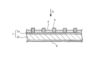
- FIG. 1 is a cross-sectional view of an essential part showing an embodiment of a solar cell manufactured using a conductive paste according to the present invention.
- an antireflection film 2 and a light receiving surface electrode 3 are formed on one main surface of a semiconductor substrate 1 containing Si as a main component, and a back electrode 4 is formed on the other main surface of the semiconductor substrate 1.
- the semiconductor substrate 1 has a p-type semiconductor layer 1b and an n-type semiconductor layer 1a, and an n-type semiconductor layer 1a is formed on the upper surface of the p-type semiconductor layer 1b.
- the semiconductor substrate 1 can be obtained, for example, by diffusing impurities on one main surface of a single-crystal or polycrystalline p-type semiconductor layer 1b to form a thin n-type semiconductor layer 1a.
- the n-type semiconductor layer 1a is formed on the upper surface of the layer 1b, its structure and manufacturing method are not particularly limited.
- the semiconductor substrate has a structure in which a thin p-type semiconductor layer is formed on one main surface of the n-type semiconductor layer, or a p-type semiconductor layer and an n-type semiconductor layer on a part of one main surface of the semiconductor substrate.
- a structure in which both are formed may be used.
- the conductive paste according to the present invention can be used effectively as long as it is the main surface of the semiconductor substrate 1 on which the antireflection film 2 is formed.
- the surface of the semiconductor substrate 1 is shown in a flat shape, but the surface is formed to have a fine concavo-convex structure in order to effectively confine sunlight to the semiconductor substrate 1.
- the antireflection film 2 is formed of an insulating material such as silicon nitride (SiNx), suppresses reflection of light to the light receiving surface indicated by arrow A, and guides sunlight to the semiconductor substrate 1 quickly and efficiently.
- the material constituting the antireflection film 2 is not limited to the above silicon nitride, and other insulating materials such as silicon oxide and titanium oxide may be used, and two or more kinds of insulating materials may be used. May be used in combination. In addition, as long as it is crystalline Si, either single crystal Si or polycrystalline Si may be used.
- the light receiving surface electrode 3 is formed on the semiconductor substrate 1 through the antireflection film 2.
- the light-receiving surface electrode 3 is formed by applying a conductive paste of the present invention, which will be described later, onto the semiconductor substrate 1 by using screen printing or the like to produce a conductive film and baking it. That is, in the baking process for forming the light receiving surface electrode 3, the antireflection film 2 under the conductive film is decomposed and removed and fired through, whereby the light receiving surface electrode is formed on the semiconductor substrate 1 so as to penetrate the antireflection film 2. 3 is formed.
- the light-receiving surface electrode 3 has a large number of finger electrodes 5a, 5b,... 5n arranged in a comb-like shape and intersects with the finger electrodes 5a, 5b,.
- the bus bar electrode 6 is provided, and the finger electrodes 5a, 5b,... 5n and the bus bar electrode 6 are electrically connected.
- the antireflection film 2 is formed in the remaining region excluding the portion where the light receiving surface electrode 3 is provided. In this way, the electric power generated in the semiconductor substrate 1 is collected by the finger electrodes 5n and taken out to the outside by the bus bar electrodes 6.
- the back electrode 4 is formed on the back surface of the current collecting electrode 7 and the current collecting electrode 7 made of Al or the like formed on the back surface of the p-type semiconductor layer 1b. It is comprised with the extraction electrode 8 which consists of Ag etc. which were electrically connected with the current collection electrode 7. FIG. Then, the electric power generated in the semiconductor substrate 1 is collected by the collecting electrode 7 and is taken out by the extracting electrode 8.
- the conductive paste of the present invention contains conductive powder, glass frit, binder resin, and organic solvent.
- the binder resin contains a thermosetting resin having a thermal decomposition end temperature of 450 to 650 ° C. in a range of 1.0 wt% or less (not including 0 wt%).
- thermoplastic resin such as a cellulose derivative typified by an ethyl cellulose resin
- ethyl cellulose resin usually disappear at the end of thermal decomposition at a temperature of 400 ° C. or lower during the baking process.
- the softening point is excessively lowered, it is excessively fluidized, and a glass component is deposited at the interface between the light-receiving surface electrode 3 and the semiconductor substrate 1 after firing, resulting in increased contact resistance. Therefore, glass frit having a softening point of 450 ° C. or higher is usually used.
- the conductive powder such as Ag starts sintering at a temperature of 450 ° C. or higher in the firing process.
- thermoplastic resin that terminates thermal decomposition at a temperature of at least 450 ° C. at which the softening of the glass frit and the sintering of the conductive powder starts is included as the binder resin.
- the thermal decomposition end temperature must be 650 ° C or lower. That is, when the end temperature of thermal decomposition exceeds 650 ° C., the thermosetting resin cannot be sufficiently thermally decomposed in the baking process, and the thermosetting resin that cannot be completely decomposed is also subjected to the light-receiving surface electrode 3 and the semiconductor even after baking. It remains at the interface with the substrate 1. For this reason, contact resistance increases between the light-receiving surface electrode 3 and the semiconductor substrate 1, and there exists a possibility of causing the battery characteristic fall of a solar cell.
- the content of the thermosetting resin needs to be 1.0% by weight (including 0% by weight) or less. This is because when the content of the thermosetting resin exceeds 1.0% by weight, the thermosetting resin cannot be sufficiently thermally decomposed in the temperature range of 450 to 650 ° C. This is because the curable resin remains at the interface between the light-receiving surface electrode 3 and the semiconductor substrate 1 even after firing, and as a result, the contact resistance between the two increases and the battery characteristics of the solar cell may be degraded.
- thermosetting resin is not particularly limited as long as it is thermally decomposed at 450 to 650 ° C.
- the alkyd resin, phenol resin, melamine resin, polyurethane resin, etc. are used. Of these, alkyd resins can be preferably used.
- the decomposition end temperature of the thermosetting resin can be set by adjusting the molecular weight of the resin and the additive substance. For example, in the case of an alkyd resin, the thermal decomposition end temperature can be adjusted by changing the type and blending ratio of the organic acid used as a raw material.
- the present invention preferably contains a cellulose derivative as the binder resin. That is, since the cellulose derivative has an action of suppressing bleeding after the conductive paste is printed, it is possible to make fine wiring. And since the light-receiving area of a solar cell increases by making it fine wiring, the solar cell which has favorable conversion efficiency can be obtained. Moreover, since the adhesive strength at a low temperature can be sufficiently secured, a solar cell having even better adhesive strength and conversion efficiency can be obtained. That is, since the cellulose derivative is a thermoplastic resin that is usually thermally decomposed and disappears at a low temperature of 400 ° C. or lower, the inclusion of the cellulose derivative together with the thermosetting resin further uses the adhesive strength and improves the conversion efficiency. A solar cell having excellent battery characteristics can be obtained.
- the total content of the cellulose derivative and the thermosetting resin needs to be in the range of 2.0% by weight or less. This is because when the total content of the thermosetting resin and the cellulose derivative exceeds 2.0% by weight, these resins cannot be fully thermally decomposed, and the thermosetting resin that has not been fully thermally decomposed receives light even after firing. This is because if it remains at the interface between the surface electrode 3 and the semiconductor substrate 1, the contact resistance between the two will increase and the battery characteristics of the solar cell may deteriorate.
- the total content of the thermosetting resin and the cellulose derivative needs to be in the range of 2.0% by weight or less.
- Such a cellulose derivative is not particularly limited, and for example, ethyl cellulose resin, cellulose acetate butyrate resin, nitrocellulose resin and the like can be used.
- the conductive paste of the present invention may contain other binder resin components such as rosin in addition to the thermosetting resin and the cellulose derivative.
- thermosetting resin preferably has an acid value of 5 KOHmg / g or more.
- the acid value is the weight (mg) of KOH required to neutralize the acidic component contained in 1 g of the thermosetting resin.
- the reason why the acid value is preferably 5 KOHmg / g or more is as follows.
- the silicon nitride when using silicon nitride (SiNx) on the anti-reflective coating composition, the silicon nitride reacts with moisture in the air, part of which forms a SiNH 2. SiNH 2 is dehydrated and condensed with the carboxyl group (—COOH) of the alkyd resin to form an amide bond, thereby improving the adhesive strength at low temperatures. And it is thought that a much better adhesive strength and conversion efficiency can be obtained because the higher the acid value, the more carboxyl groups.
- the acid value of the thermosetting resin is preferably 5 KOHmg / g or more.
- the lead-free glass frit causes excessive flow when the softening point of the glass frit is excessively lowered as compared with the lead-based glass frit, it is necessary to use a glass frit having a softening point of 450 ° C. or higher.
- thermosetting resin that is thermally decomposed at 450 to 650 ° C. is contained in the conductive paste, the thermal decomposition of the binder resin is completed after the softening of the glass frit is started.
- the present invention is particularly effective when such a lead-free glass frit is used.
- a lead-free glass frit for example, a Si—B—Bi—M glass frit (M is an alkaline earth metal) can be used.
- the Bi content is preferably 30 mol% or less in terms of Bi 2 O 3 .
- the conductive powder is not particularly limited as long as it is a metal powder having good conductivity, but good conductivity without being oxidized even when the baking treatment is performed in the air. Ag powder that can maintain the viscosity can be preferably used.
- the shape of the conductive powder is not particularly limited, and may be, for example, a spherical shape, a flat shape, an irregular shape, or a mixed powder thereof.
- the average particle diameter of the conductive powder is not particularly limited, but from the viewpoint of securing a desired contact point between the conductive powder and the semiconductor substrate 1, in terms of spherical powder, 1. 0 to 5.0 ⁇ m is preferable.
- ZnO facilitates the decomposition and removal of the antireflection film formed in advance on the surface of the semiconductor substrate 1 when firing the conductive paste, thereby enabling smooth fire-through.
- the light-receiving surface electrode 3 and the semiconductor substrate 1 Reduce the contact resistance.
- the decomposition action of the antireflection film occurs at a location where the conductive powder and ZnO are in contact.
- plasticizers such as di-2-ethylhexyl phthalate and dibutyl phthalate as necessary to the conductive paste.
- plasticizers such as di-2-ethylhexyl phthalate and dibutyl phthalate
- a thixotropic agent, a thickener, a dispersant, and the like may be added, and a rheology adjuster such as a fatty acid amide or a fatty acid may be added as necessary.
- this conductive paste is weighed so that the conductive powder, glass frit, binder resin, and organic solvent have a predetermined mixing ratio, and dispersed and kneaded in the organic vehicle using a three-roll mill or the like. Thus, it can be easily manufactured.
- the binder resin and the organic solvent are blended so that the volume ratio is, for example, 1 to 3: 7 to 9.
- the alkyd resin that includes conductive powder such as Ag powder, glass frit, binder resin, and solvent, and the thermal decomposition finishes at a temperature of 450 to 650 ° C.
- the content of the thermosetting resin is 1.0% by weight or less (not including 0% by weight) in the paste.
- the thermosetting resin is cured until it reaches the temperature range where the softening of the glass frit and the sintering of the conductive powder starts, and the semiconductor substrate and the conductive surface electrode are electrically conductive. Adhesiveness with the film can be ensured, and conversion efficiency can be improved. In addition, the adhesive strength between the light-receiving surface electrode and the semiconductor substrate can be improved even after firing.
- the binder resin contains a cellulose derivative, and the total content of the thermosetting resin and the cellulose derivative is 2.0% by weight or less, thereby printing the conductive paste. Bleeding can be effectively suppressed, and fine wiring can be achieved. And the light-receiving area of a solar cell increases by making it fine wiring in this way, As a result, the solar cell which has favorable conversion efficiency can be obtained. And since the adhesive strength in low temperature can also be ensured enough, the solar cell which has much more favorable adhesive strength and conversion efficiency can be obtained.
- thermosetting resin has an acid value of 5 KOHmg / g or more, the adhesive strength can be improved more effectively.
- the glass frit contains Bi in a range of less than 30 mol% in terms of Bi 2 O 3 and does not contain Pb, thereby using a lead-free conductive paste. Even if it exists, the conversion efficiency can be further improved.
- FIG. 4 is a manufacturing process diagram showing an embodiment of a method for manufacturing a solar cell.
- a p-type semiconductor substrate 11 made of monocrystalline or polycrystalline Si or the like and having a thickness of about 200 mm is prepared.
- the p-type semiconductor substrate 11 is obtained, for example, by cutting an ingot formed by melting and re-solidifying a semiconductor raw material such as Si in a crucible for each block and slicing it into a thin piece with a wire saw or the like.
- an n-type diffusion layer 12 is formed on the surface of the p-type semiconductor substrate 11. That is, a coating solution containing an impurity to be diffused is applied in a film shape by spin coating or the like to form a coating film, and heat treatment is performed to diffuse the impurities on the surface of the p-type semiconductor substrate 11, and the thickness is 300. An n-type diffusion layer 12 of ⁇ 500 nm is formed. Thus, a semiconductor substrate 1 is obtained in which the p-type semiconductor substrate 11 is a p-type semiconductor layer 1b and the n-type diffusion layer 12 is an n-type semiconductor layer 1a (formation of a pn junction).
- the impurity to be diffused is not particularly limited as long as it can form the n-type diffusion layer 12, but P is usually preferred and phosphorus oxychloride (POCl 3 ) is preferred as the coating solution. Is done. Further, in order to effectively confine incident sunlight in the semiconductor substrate 1, it is preferable to perform texture etching to make the surface have a micro uneven structure.
- the film thickness of an insulating material such as silicon nitride (SiNx) is 70 to 80 nm.
- An antireflection film 2 is formed.
- an Al paste containing Al powder having an average particle diameter of 5 ⁇ m is prepared, and further an Ag paste containing Ag powder having an average particle diameter of 1.5 ⁇ m is prepared.
- the Al paste is applied to the entire back surface of the semiconductor substrate 1, and the Ag paste is screen-printed and dried to form the second conductive film 13 for the back electrode as shown in FIG. To do.
- screen printing is performed using the conductive paste of the present invention to form the first conductive film 14 having a predetermined pattern.
- the first and second firing profiles are such that Al is sintered at 500 ° C. and the maximum firing temperature is 750 ° C.
- the light-receiving surface electrode 3 and the back surface electrode 4 are produced, and a solar cell is formed.
- the thermosetting resin contained in the conductive paste of the present invention is thermally decomposed at 450 to 650 ° C. and disappears during the baking process.
- baking step is performed when the thermosetting resin is 450. Decomposes and disappears in a temperature range of ⁇ 650 ° C. Excellent solar cell efficiency can be easily obtained.
- the present invention is not limited to the above embodiment.
- the B—Si—Bi—M glass frit is exemplified as the glass frit.
- the glass frit is not limited to this.
- alkali metal oxides Li 2 O, Na 2 O, K 2 O
- various oxides such as TiO 2 and ZrO 2 .
- Example preparation Measurement of decomposition end temperature
- TG-DTA thermogravimetric-differential thermal analyzer
- ethyl cellulose resin as a cellulose derivative was prepared, and the decomposition end temperature was determined using TG-DTA as described above, and it was 365 ° C.
- the alkyd resin was dissolved in an alcohol / ether mixture, and the acid value was measured by titration with a 0.1N alcoholic potassium hydroxide solution using a phenolphthalein reagent as an indicator.
- a spherical Ag powder having an average particle diameter of 1.0 ⁇ m as a conductive powder, and a Si—B—Bi—Ba-based glass frit prepared with a molar content of Bi 2 O 3 in the glass frit of 26 mol% were prepared. .
- the alkyd resin is weighed so that the glass frit is 2.5 parts by weight with respect to 100 parts by weight of the Ag powder, and the alkyd resin and ethyl cellulose resin are contained in the conductive paste as shown in Table 1. Then, the ethylcellulose resin was weighed, mixed with texanol as a solvent in a planetary mixer, dispersed with a three-roll mill, and kneaded to prepare conductive pastes of sample numbers 1 to 10.
- an antireflection film having a thickness of 80 nm was formed by plasma enhanced chemical vapor deposition (PECVD) over the entire surface of a single crystal Si-based semiconductor substrate having a length of 50 mm, a width of 50 mm, and a thickness of 0.18 mm.
- PECVD plasma enhanced chemical vapor deposition
- P is diffused into a part of the p-type Si-based semiconductor layer, whereby an n-type Si-based semiconductor layer is formed on the upper surface of the p-type Si-based semiconductor layer.
- spherical Al powder having an average particle diameter of 5 ⁇ m and Pb—Si glass frit were prepared. Then, 3.7 parts by weight of the above glass frit is mixed with 100 parts by weight of Al powder, and further weighed so that the ethyl cellulose resin is 4.6% by weight in the conductive paste, and in a planetary mixer together with texanol as a solvent. And then dispersed with a three-roll mill to produce an Al paste.
- spherical Ag powder having an average particle diameter of 1.5 ⁇ m and Si—B—Bi glass frit were prepared. Then, 3 parts by weight of the glass frit is mixed with 100 parts by weight of Ag powder, and further weighed so that the ethylcellulose resin is 3% by weight in the conductive paste, and mixed in a planetary mixer together with texanol as a solvent, Ag paste was produced by dispersing with a three-roll mill.
- an Al paste is applied to the entire back surface of the semiconductor substrate 1 so that the film thickness after firing is 10 ⁇ m, and further, Ag paste is screen-printed and dried so that the film thickness after firing is 10 ⁇ m.
- a second conductive film mainly composed of Al and Ag was produced for the electrode. And it dried in the oven set to 150 degreeC. Thereafter, the conductive paste was screen-printed on the antireflection film to produce a first conductive film so that the film thickness after baking was 20 ⁇ m, and dried in an oven set at 150 ° C.
- the conveyance speed is adjusted so that the sample passes between the inlet and the outlet in about 1 minute, and the maximum firing temperature is 750 ° C. in an air atmosphere.
- the first and second conductive films were sintered to form the light-receiving surface electrodes, thereby preparing samples Nos. 1 to 10.
- sample evaluation The adhesive strength was measured for each of sample numbers 1 to 10. That is, the lead wire in which the core wire Cu was coated with Sn—Ag—Cu solder was soldered to the light-receiving surface electrode of each sample.
- Table 1 shows the content of alkyd resin and ethyl cellulose resin, decomposition end temperature, acid value, adhesive strength, and conversion efficiency ⁇ .
- the conversion efficiency ⁇ was expressed as a relative value with the sample number 1 being 100%. A sufficient power generation amount can be obtained when the relative value is 98.0% or more.
- Sample No. 6 had a low adhesive strength of 2001 mN, and the conversion efficiency ⁇ was also reduced to 83.3% relative to Sample No. 1. This is probably because the conductive paste does not contain an alkyd resin, so that ethyl cellulose alone cannot sufficiently secure the adhesion between the light-receiving surface electrode and the semiconductor substrate in the baking process.
- Sample No. 7 had a sufficient adhesive strength of 4178 mN, but the conversion efficiency ⁇ decreased to 88.1% with respect to Sample No. 1. This is because the alkyd resin content in the conductive paste is 2.0% by weight and exceeds 1.0% by weight, so that the alkyd resin cannot be fully thermally decomposed and cannot be completely decomposed. It is considered that the alkyd resin remained at the interface between the light-receiving surface electrode and the semiconductor substrate even after firing, thereby increasing the contact resistance at the interface and reducing the conversion efficiency ⁇ .
- Sample No. 8 had an adhesive strength as low as 1981 mN, and the conversion efficiency ⁇ also decreased to 89.0% with respect to Sample No. 1. This is because the decomposition end temperature of the alkyd resin is 435 ° C. and is as low as less than 450 ° C., so the alkyd resin is thermally decomposed before the softening of the glass frit starts or before the Ag powder starts sintering. This seems to be because sufficient adhesion between the light-receiving surface electrode and the semiconductor substrate cannot be secured.
- Sample No. 9 had a sufficient adhesive strength of 3609 mN, but the conversion efficiency ⁇ decreased to 83.2% with respect to Sample No. 1. This is because the thermal decomposition end temperature of the alkyd resin is 680 ° C. and exceeds 650 ° C., the alkyd resin cannot be fully thermally decomposed, and the alkyd resin that has not been completely thermally decomposed is fired even after firing. It is considered that it remains at the interface with the substrate, which increases the contact resistance at the interface and lowers the conversion efficiency ⁇ .
- Sample No. 10 had a sufficient adhesive strength of 4658 mN, but the conversion efficiency ⁇ decreased to 87.0% with respect to Sample No. 1. This is because the total content of the alkyd resin and ethyl cellulose resin exceeds 2.0% by weight, so that a part of the alkyd resin remains without being thermally decomposed. It remains at the interface between the electrode and the semiconductor substrate, which increases the contact resistance at the interface and thus leads to a decrease in conversion efficiency ⁇ .
- the decomposition end temperature of the alkyd resin is 589 ° C.
- the content of the alkyd resin is 1.0% by weight or less
- the adhesive strength is 3690-4786 mN, far exceeding 2940 mN
- the conversion efficiency ⁇ is 98.6% or more. It was found that solar cells with good battery characteristics can be obtained.
- conductive pastes and solar cells of sample numbers 21 to 26 were prepared by the same method and procedure as in Example 1, and the adhesive strength and conversion efficiency ⁇ of each sample were obtained.
- Table 2 shows the contents of alkyd resin and ethyl cellulose resin of sample numbers 21 to 26, decomposition end temperature, acid value, adhesive strength, and conversion efficiency ⁇ .
- the decomposition end temperature of the alkyd resin is 452 to 649 ° C.
- the content of the alkyd resin is 1.0% by weight or less
- the total amount of the alkyd resin and ethyl cellulose is 2.0% by weight or less. Therefore, the adhesive strength exceeded 2940 mN, and the conversion efficiency ⁇ was 99.8% or higher, and a solar cell with good battery characteristics could be obtained.
- sample numbers 25 and 26 have acid values of 3.7, 4.7, and 5 or less, respectively, it was found that the adhesive strength tends to decrease slightly.
- the conductive pastes and solar cells of sample numbers 31 to 33 were prepared by the same method and procedure as in Example 1, and the adhesive strength and conversion efficiency ⁇ of each sample were prepared. Asked.
- Table 3 shows the contents of the alkyd resin and ethyl cellulose resin of sample numbers 31 to 33, the decomposition end temperature, the acid value, the adhesive strength, and the conversion efficiency ⁇ .
- the decomposition end temperature of the alkyd resin is 589 ° C.
- the content of the alkyd resin is 0.5% by weight
- the total content of the alkyd resin and the ethyl cellulose resin is 1.0% by weight. %
- the adhesive strength was 4197 to 4413 mN
- the conversion efficiency ⁇ was 98.5% or more, and a solar cell with good battery characteristics could be obtained.
- Sample Nos. 31 to 33 have a Bi 2 O 3 content of 29.5 to 32.0 mol%, which exceeds 26.0 mol%. It turned out that it becomes a downward tendency.
- a solar cell having high adhesion strength between the light-receiving surface electrode and the semiconductor substrate and capable of obtaining good conversion efficiency can be realized.
Landscapes
- Physics & Mathematics (AREA)
- Chemical & Material Sciences (AREA)
- Dispersion Chemistry (AREA)
- Spectroscopy & Molecular Physics (AREA)
- Photovoltaic Devices (AREA)
- Conductive Materials (AREA)
Abstract
L'invention concerne une pâte conductrice qui contient une poudre d'Ag, une fritte de verre, une résine thermodurcissable et un solvant. La décomposition thermique de la résine thermodurcissable se termine à une température de 450 à 650 °C, et la résine thermodurcissable est contenue dans la pâte à hauteur de 1,0 % en poids ou moins (à l'exception de 0 % en poids). Dans des cas où un dérivé de cellulose est contenu dans la pâte conductrice, la teneur totale de la résine thermodurcissable et du dérivé de cellulose est de 2,0 % en poids ou moins. Une électrode de surface réceptrice de lumière (3) est formée à l'aide de la pâte conductrice. En conséquence, on peut obtenir : une pâte conductrice permettant de former une électrode pour des photopiles, qui permet d'obtenir une importante résistance de liaison entre une électrode de surface réceptrice de lumière et un substrat de semi-conducteur, et qui permet d'atteindre un bon rendement de conversion ; une photopile qui est fabriquée à l'aide de la pâte conductrice ; et un procédé de fabrication d'une photopile.
Priority Applications (1)
| Application Number | Priority Date | Filing Date | Title |
|---|---|---|---|
| JP2012557898A JP5403304B2 (ja) | 2011-02-16 | 2012-02-07 | 導電性ペースト、太陽電池、及び太陽電池の製造方法 |
Applications Claiming Priority (2)
| Application Number | Priority Date | Filing Date | Title |
|---|---|---|---|
| JP2011030704 | 2011-02-16 | ||
| JP2011-030704 | 2011-02-16 |
Publications (1)
| Publication Number | Publication Date |
|---|---|
| WO2012111479A1 true WO2012111479A1 (fr) | 2012-08-23 |
Family
ID=46672407
Family Applications (1)
| Application Number | Title | Priority Date | Filing Date |
|---|---|---|---|
| PCT/JP2012/052707 Ceased WO2012111479A1 (fr) | 2011-02-16 | 2012-02-07 | Pâte conductrice, photopile et procédé de fabrication d'une photopile |
Country Status (3)
| Country | Link |
|---|---|
| JP (1) | JP5403304B2 (fr) |
| TW (1) | TW201243867A (fr) |
| WO (1) | WO2012111479A1 (fr) |
Cited By (3)
| Publication number | Priority date | Publication date | Assignee | Title |
|---|---|---|---|---|
| JP2014086217A (ja) * | 2012-10-22 | 2014-05-12 | Taiyo Holdings Co Ltd | 導電性組成物、電極、プラズマディスプレイパネル及びタッチパネル |
| JPWO2020195522A1 (fr) * | 2019-03-28 | 2020-10-01 | ||
| JPWO2020195523A1 (fr) * | 2019-03-28 | 2020-10-01 |
Citations (4)
| Publication number | Priority date | Publication date | Assignee | Title |
|---|---|---|---|---|
| JP2001202822A (ja) * | 2000-01-21 | 2001-07-27 | Murata Mfg Co Ltd | 導電性ペースト |
| JP2003165744A (ja) * | 2001-11-26 | 2003-06-10 | Murata Mfg Co Ltd | 導電性ペースト |
| JP2004134775A (ja) * | 2002-09-19 | 2004-04-30 | Murata Mfg Co Ltd | 導電性ペースト |
| WO2007102287A1 (fr) * | 2006-03-07 | 2007-09-13 | Murata Manufacturing Co., Ltd. | Pate conductrice et cellule solaire |
Family Cites Families (1)
| Publication number | Priority date | Publication date | Assignee | Title |
|---|---|---|---|---|
| JP2012248790A (ja) * | 2011-05-31 | 2012-12-13 | Yokohama Rubber Co Ltd:The | 太陽電池集電電極形成用導電性組成物および太陽電池セル |
-
2012
- 2012-02-07 WO PCT/JP2012/052707 patent/WO2012111479A1/fr not_active Ceased
- 2012-02-07 JP JP2012557898A patent/JP5403304B2/ja not_active Expired - Fee Related
- 2012-02-14 TW TW101104778A patent/TW201243867A/zh unknown
Patent Citations (4)
| Publication number | Priority date | Publication date | Assignee | Title |
|---|---|---|---|---|
| JP2001202822A (ja) * | 2000-01-21 | 2001-07-27 | Murata Mfg Co Ltd | 導電性ペースト |
| JP2003165744A (ja) * | 2001-11-26 | 2003-06-10 | Murata Mfg Co Ltd | 導電性ペースト |
| JP2004134775A (ja) * | 2002-09-19 | 2004-04-30 | Murata Mfg Co Ltd | 導電性ペースト |
| WO2007102287A1 (fr) * | 2006-03-07 | 2007-09-13 | Murata Manufacturing Co., Ltd. | Pate conductrice et cellule solaire |
Cited By (5)
| Publication number | Priority date | Publication date | Assignee | Title |
|---|---|---|---|---|
| JP2014086217A (ja) * | 2012-10-22 | 2014-05-12 | Taiyo Holdings Co Ltd | 導電性組成物、電極、プラズマディスプレイパネル及びタッチパネル |
| JPWO2020195522A1 (fr) * | 2019-03-28 | 2020-10-01 | ||
| JPWO2020195523A1 (fr) * | 2019-03-28 | 2020-10-01 | ||
| JP7136334B2 (ja) | 2019-03-28 | 2022-09-13 | 株式会社村田製作所 | チップ型セラミック電子部品およびその製造方法 |
| JP7136333B2 (ja) | 2019-03-28 | 2022-09-13 | 株式会社村田製作所 | チップ型セラミック電子部品およびその製造方法 |
Also Published As
| Publication number | Publication date |
|---|---|
| JPWO2012111479A1 (ja) | 2014-07-03 |
| JP5403304B2 (ja) | 2014-01-29 |
| TW201243867A (en) | 2012-11-01 |
Similar Documents
| Publication | Publication Date | Title |
|---|---|---|
| JP5349738B2 (ja) | 半導体デバイスの製造方法、およびそこで使用される導電性組成物 | |
| CN1862839B (zh) | 半导体器件的制造方法及其中用到的导电组合物 | |
| TW201035260A (en) | Conductive paste for solar cell electrode | |
| US8884277B2 (en) | Thick film conductive composition and use thereof | |
| JP6714275B2 (ja) | 導電性ペースト及び太陽電池 | |
| JP2013239695A (ja) | 酸化アンチモンを含有する厚膜組成物および半導体デバイスの製造におけるその使用 | |
| JP2014533432A (ja) | Lfc−percシリコン太陽電池の製造方法 | |
| CN108701504A (zh) | 导电性糊剂和太阳能电池 | |
| JP2010087501A (ja) | 導電性組成物及びそれを用いた太陽電池 | |
| TWI725035B (zh) | 導電性膠、太陽能電池及太陽能電池的製造方法 | |
| JP7027025B2 (ja) | 導電性組成物 | |
| JP2010251645A (ja) | 太陽電池及びその電極形成用導電性ペースト | |
| JP5403304B2 (ja) | 導電性ペースト、太陽電池、及び太陽電池の製造方法 | |
| WO2012111478A1 (fr) | Pâte conductrice et photopile | |
| JP4907331B2 (ja) | 光電変換素子用導電性ペースト、光電変換素子、および光電変換素子の作製方法 | |
| WO2014050704A1 (fr) | Pâte conductrice et cellule solaire | |
| JP2013243279A (ja) | 太陽電池の電極形成用導電性ペースト | |
| JP2014078594A (ja) | ペースト組成物と太陽電池 | |
| WO2024101223A1 (fr) | Pâte électriquement conductrice, cellule solaire, et procédé destiné à fabriquer une cellule solaire | |
| JP6266079B2 (ja) | 太陽電池の電極形成用導電性ペースト及び太陽電池の製造方法 | |
| JP6200128B2 (ja) | 太陽電池の電極形成用導電性ペースト | |
| WO2012160921A1 (fr) | Pâte conductrice et cellule solaire | |
| JP4970026B2 (ja) | 光電変換素子用導電性ペースト、光電変換素子、および光電変換素子の作製方法 | |
| KR20250108642A (ko) | 태양 전지 | |
| WO2024257439A1 (fr) | Pâte électroconductrice, utilisation de pâte électroconductrice, cellule solaire et procédé de production de cellule solaire |
Legal Events
| Date | Code | Title | Description |
|---|---|---|---|
| 121 | Ep: the epo has been informed by wipo that ep was designated in this application |
Ref document number: 12747096 Country of ref document: EP Kind code of ref document: A1 |
|
| ENP | Entry into the national phase |
Ref document number: 2012557898 Country of ref document: JP Kind code of ref document: A |
|
| NENP | Non-entry into the national phase |
Ref country code: DE |
|
| 122 | Ep: pct application non-entry in european phase |
Ref document number: 12747096 Country of ref document: EP Kind code of ref document: A1 |