WO2012114392A1 - Circuit de protection d'entrée - Google Patents
Circuit de protection d'entrée Download PDFInfo
- Publication number
- WO2012114392A1 WO2012114392A1 PCT/JP2011/004197 JP2011004197W WO2012114392A1 WO 2012114392 A1 WO2012114392 A1 WO 2012114392A1 JP 2011004197 W JP2011004197 W JP 2011004197W WO 2012114392 A1 WO2012114392 A1 WO 2012114392A1
- Authority
- WO
- WIPO (PCT)
- Prior art keywords
- protection circuit
- impedance
- terminal
- termination
- input protection
- Prior art date
- Legal status (The legal status is an assumption and is not a legal conclusion. Google has not performed a legal analysis and makes no representation as to the accuracy of the status listed.)
- Ceased
Links
Images


Classifications
-
- H—ELECTRICITY
- H02—GENERATION; CONVERSION OR DISTRIBUTION OF ELECTRIC POWER
- H02H—EMERGENCY PROTECTIVE CIRCUIT ARRANGEMENTS
- H02H3/00—Emergency protective circuit arrangements for automatic disconnection directly responsive to an undesired change from normal electric working condition with or without subsequent reconnection ; integrated protection
- H02H3/20—Emergency protective circuit arrangements for automatic disconnection directly responsive to an undesired change from normal electric working condition with or without subsequent reconnection ; integrated protection responsive to excess voltage
-
- H—ELECTRICITY
- H03—ELECTRONIC CIRCUITRY
- H03K—PULSE TECHNIQUE
- H03K19/00—Logic circuits, i.e. having at least two inputs acting on one output; Inverting circuits
- H03K19/0005—Modifications of input or output impedance
-
- H—ELECTRICITY
- H03—ELECTRONIC CIRCUITRY
- H03K—PULSE TECHNIQUE
- H03K19/00—Logic circuits, i.e. having at least two inputs acting on one output; Inverting circuits
- H03K19/0175—Coupling arrangements; Interface arrangements
- H03K19/017545—Coupling arrangements; Impedance matching circuits
Definitions
- the present invention relates to an input protection circuit for a low-amplitude interface circuit, and more particularly to an unintended high-voltage pull-up protection for a low-voltage interface circuit between mobile memory cards inserted in a host device having a combo socket.
- a low amplitude interface For Gbps class data transmission, a low amplitude interface is generally used.
- low-amplitude differential interfaces are widely used in applications in which noise resistance and radiated electromagnetic wave restrictions are strictly demanded, for example, LVDS (Low Voltage Voltage Differential Driver) transmission system.
- LVDS Low Voltage Voltage Differential Driver
- a constant current of about 3.5 mA flows through the differential termination resistor 100 ⁇ on the receiving side, so that the amplitude on the receiving side is guaranteed while establishing impedance matching with the signal transmission line.
- impedance matching As a result, there is an advantage that the received signal quality can be improved.
- the signal amplitude is set around 300 mV.
- the power supply voltage of the interface circuit it is possible to reduce the power supply voltage of the interface circuit to around 1 V, and one of the merits is that the power reduction effect can be obtained.
- the supplier of the personal computer is equipped with a card reader device equipped with a mechanism called a combo socket that is devised so that a plurality of different types of mobile memory cards can be handled with one opening.
- a combo socket that is devised so that a plurality of different types of mobile memory cards can be handled with one opening.
- the electrode terminal provided on the socket side has a spring shape to press against the terminal electrode on the mobile memory card side to reduce contact resistance.
- an existing SD card or MMC uses a 3.3V single-ended interface, but when the interface voltage is lowered to reduce power consumption, the combo socket has 1 as the power supply voltage. Terminals for mobile memory cards equipped with an interface using .8V or 1.2V will be mixed, and the problem of destruction due to excess withstand voltage will become apparent. This is a problem directly related to the reliability and safety of the product and cannot be ignored.
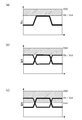
- FIG. 14 shows an example of a diode clamp circuit.
- FIG. 14A uses a forward connection of junction diodes.
- the clamp circuit 20 is composed of a diode 21.
- the role of the diode 21 is to fix the terminal voltage to be displaced beyond the threshold voltage V F by utilizing the electrical characteristics that the resistance between the terminals becomes low when the forward voltage becomes the threshold voltage V F or more. It is to be.
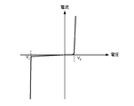
- FIG. 15 shows the electrical characteristics of the diode.
- FIG. 14B shows a case where a Zener diode is used for the clamp circuit 20.
- the clamp circuit 20 in the figure is configured by connecting the Zener diodes 22 in the reverse direction, and the role of the Zener diodes 22 is to make use of electrical characteristics that the Zener breakdown voltage VZ or less is low resistance between the diode terminals. This is to fix the voltage at which the terminal voltage tends to be displaced more than
- the threshold voltage of the diode is lower than the upper limit voltage of the low amplitude interface signal, the clamp diode is turned on at the time of signal transmission, and the resistance becomes low. At this time, the signal waveform is clamped, and when viewed as a terminal impedance, the low resistance of the diode becomes dominant, so that a reflected wave in which the sign of the signal voltage waveform is inverted is generated, and the reflected wave passes through the transmission line. It also causes EMI (Electro Magnetic Interference) due to propagation.
- EMI Electro Magnetic Interference
- the threshold voltage of the diode does not exceed the withstand voltage of the internal device but exceeds the power supply voltage of the low-amplitude interface circuit, the potential at the signal terminal when a high voltage is applied from the outside Will exceed the power supply voltage.
- the low-amplitude interface circuit is composed of CMOS
- the P-channel MOS transistor whose gate terminal is connected to the external terminal is exposed to a characteristic deterioration condition called PBTI (Positive Bias Temperature Instability).
- PBTI Positive Bias Temperature Instability
- a method of controlling the clamp voltage with high accuracy for example, as in Patent Document 1, a method of forming a source voltage follower circuit with a MOS transistor and a differential amplifier and determining the clamp voltage with a reference voltage is effective.
- Patent Document 1 has a problem of input capacity.
- a depletion layer capacitance is added as a terminal capacitance. Since the interface circuit is exposed to the external environment by its terminal electrode and receives electrostatic discharge or the like, a protection circuit is provided by separately added components such as a diode element and a varistor on the integrated circuit. The total capacity of the protection circuit and the interface circuit component itself from the beginning exists as a terminal capacity unique to the system. The terminal capacitance works to lower the input / output impedance for high-frequency signal components.
- the absolute value of the synthesized impedance with the termination device is lowered and the complex impedance is complex.
- the corner is shifted from the impedance originally possessed by the termination device. If the complex angle of the impedance of the terminator is shifted, this alone causes impedance mismatching, and thus the influence on the signal quality begins to appear. Furthermore, if the frequency rises and the impedance of the terminal capacitance is lower than the impedance of the termination device, the impedance of the terminal capacitance portion becomes dominant, and the range of impedance values assumed by the termination device falls outside.
- the present invention solves the above-described problems, and an object thereof is to provide a diode element in an input protection circuit in which a termination device is connected to an external terminal of an interface circuit, and is caused by terminal contact with the external terminal.
- a protection circuit having a configuration in which a resistance element and a diode element are connected in series is inserted in parallel with the termination device of the interface circuit.
- the resistance element of the protection circuit functions as a pull-down circuit, while an input signal during normal low amplitude signal transmission has a high impedance.
- the impedance characteristics of the termination device are not affected.
- the input protection circuit includes an external terminal, and when the external terminal is connected to a voltage source exceeding an allowable voltage to be applied via a resistor, the input protection circuit is connected to the external terminal.
- An input protection circuit for limiting a voltage applied to the amplitude interface circuit comprising: a termination device connected to the external terminal; and a protection circuit connected in parallel to the termination device, And a resistance element having one end connected to the external terminal, and a diode element having the other end connected to the anode terminal and a cathode terminal connected to a reference potential terminal.
- a termination impedance obtained in a frequency range in which the termination device desires to be matched is a real value, and a resistance value of a resistance element of the protection circuit
- the absolute value of the combined parallel impedance of the impedance of the resistance element of the protection circuit and the termination impedance obtained in the frequency range that the termination device desires to match is the absolute value of the termination impedance from the absolute value of the termination impedance. It is set so as to be within a predetermined fluctuation range.
- the predetermined variation range of the absolute value of the termination impedance is a variation range of 5% or less.
- the resistance value of the resistance element of the protection circuit is a termination obtained in a frequency range in which the impedance of the resistance element and the termination device are desired to be matched.
- the absolute value of the combined parallel impedance with the impedance falls within a fluctuation range within 3% from the absolute value of the terminal impedance, and the phase difference between the complex angle of the combined parallel impedance and the complex angle of the terminal impedance is 2 It is characterized in that it is set so as to be within degrees.
- the diode element is composed of a MOS transistor element on a semiconductor integrated circuit.
- the low-amplitude interface circuit is a differential interface circuit
- both ends of the termination device are differential signal terminals of the differential interface circuit.
- a series connection circuit of the resistance element and the diode element is connected to one or both of the differential signal pair.
- an input protection circuit comprising: an external terminal; and a low-amplitude interface circuit connected to the external terminal when the external terminal is connected to a voltage source exceeding an applied allowable voltage via a resistor.
- An input protection circuit for limiting an applied voltage comprising: a termination device connected to the external terminal; and a protection circuit connected in parallel to the termination device, wherein the protection circuit includes the external terminal A resistance element having one end connected to the N-type MOS transistor, an N-type MOS transistor having the other end connected to the drain terminal and a source terminal connected to a reference potential terminal, and an output terminal being the gate of the N-type MOS transistor.
- the non-inverting input terminal is connected to the drain terminal of the N-type MOS transistor, and the reference voltage generated by the reference voltage generating device is applied to the inverting input terminal. Characterized in that it comprises a differential amplifier with.
- a termination impedance obtained in a frequency range in which the termination device desires matching is a real value, and a resistance value of a resistance element of the protection circuit
- the absolute value of the combined parallel impedance of the impedance of the resistance element of the protection circuit and the termination impedance obtained in the frequency range that the termination device desires to match is the absolute value of the termination impedance from the absolute value of the termination impedance. It is set so as to be within a predetermined fluctuation range.
- the invention according to claim 9 is the input protection circuit according to claim 8, wherein the predetermined variation range of the absolute value of the termination impedance is a variation range of 5% or less.
- the resistance value of the resistance element of the protection circuit is a termination obtained in a frequency range in which the impedance of the resistance element and the termination device are desired to be matched.
- the absolute value of the combined parallel impedance with the impedance falls within a fluctuation range within 3% from the absolute value of the terminal impedance, and the phase difference between the complex angle of the combined parallel impedance and the complex angle of the terminal impedance is 2 It is characterized in that it is set so as to be within degrees.
- An input protection circuit includes an external terminal pair, and when one or both of the external terminal pairs are connected to a voltage source that exceeds an applied allowable voltage through a resistor, one of the external terminal pairs. Or an input protection circuit for limiting a voltage applied to a low-amplitude interface circuit connected to both, a termination device connected between the pair of external terminals, and a protection connected in parallel to the termination device
- the protection circuit includes a resistance element having one end connected to an impedance midpoint of the termination device, the other end of the resistance element connected to an anode terminal, and a cathode terminal connected to a ground terminal. And a diode element.
- an electrical connection state and a disconnection state between the external terminal pair via the termination device are provided at an impedance intermediate point of the termination device.
- a switch which can be switched is provided, and a series connection circuit of the resistance element and the diode element is connected to each of both terminals of the switch.
- the diode element of the protection circuit is formed of a MOS transistor element on a semiconductor integrated circuit.
- a protection circuit configured by connecting a resistance element and a diode element in series and inserted in parallel with the termination device.
- the anode side of the diode element of the protection circuit is charged through the resistance element of the protection circuit, and when the threshold value of the diode element is exceeded, it is turned on and energized.
- the current characteristic of the diode element exhibits a low impedance characteristic when the threshold voltage V F is exceeded.
- the voltage on the anode side of the diode element remains in the vicinity of the threshold value, and the external voltage And the threshold voltage are covered by a pull-up resistor connected to the external voltage side and a resistance element of the protection circuit.
- the method of determining the resistance value of the resistance element of the protection circuit is important in the present invention. .
- the protection circuit operates at an intermediate value between the interface power supply potential and the reference potential. If the maximum value of the signal potential does not exceed the threshold value of the diode element, the diode element is turned off and no current flows, and the impedance on the protection circuit side is high, so the influence on the termination parameter is negligible. When the threshold voltage of the diode element is exceeded, a slight direct current is generated, but the influence on the termination parameter is negligible and the influence on the signal component that is an alternating current can be suppressed.
- the interface circuit is a differential interface circuit in which a termination resistor is connected between the non-inverted signal and the inverted signal, a resistor element and a diode element are connected in series to one or both of the differential signal terminals.
- the same effect can be obtained by inserting the protective element.
- a configuration that is more effective is a configuration in which a protection circuit is inserted at a node corresponding to the midpoint of the termination impedance value.
- the effect as the protection circuit can be obtained similarly only by adding 1/2 of the termination resistance value as the resistance element of the protection circuit.
- the impedance intermediate node of the termination device is treated as AC grounding. For this reason, even if an element having any impedance value is inserted between the impedance intermediate node of the termination device and the ground potential, it is possible to eliminate the influence on the AC operation.
- a common voltage is applied to the impedance intermediate node of the termination device when a low-amplitude signal is transmitted / received, but the common voltage is always lower than the maximum value of the signal potential, and generally the fluctuation range of the signal potential is the common potential. Since 1/2 of the fluctuation width of the signal amplitude is added to the fluctuation width of the common potential, the fluctuation width of the common potential becomes narrower.
- the present invention can maximize the design margin of the protection circuit from the low signal potential and the small fluctuation range, and has a more excellent configuration.
- the resistance element connected in series with the diode element keeps the input voltage below the breakdown voltage and keeps the impedance of the protection circuit high during normal use. Can be prevented.
- the protection function can be realized at a lower cost by forming the input protection circuit on the semiconductor integrated circuit device.
- a protection circuit in which a resistance element and a diode element are connected in series at the center of the termination device can be provided to achieve a desired protection function and maintain signal quality. Is possible.
- FIG. 1 is a diagram showing the configuration of the first embodiment of the input protection circuit according to the first embodiment of the present invention.
- FIG. 2 is a diagram showing a specific configuration of a diode element of a protection circuit provided in the input protection circuit.
- FIG. 3 shows a configuration example of the termination device, where FIG. 3A is a diagram configured with pure resistance, FIG. 3B is a diagram configured with direct connection of resistance and capacitance, and FIG. It is the figure comprised by the direct connection with an inductor.
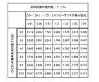
- FIG. 4 is the absolute value of the reflection coefficient for the ratio Zr and their complex angular phase difference theta d of the absolute value of the terminal impedance Z tt characteristic impedance Z0 and the terminal device of the transmission line
- FIG. 5 is a diagram showing a configuration of an input protection circuit for a differential interface circuit showing a modification of the embodiment.
- FIG. 6 is a diagram showing a specific configuration of a diode element of a protection circuit provided in the input protection circuit.
- FIG. 7 is a diagram showing the configuration of the input protection circuit according to the second embodiment of the present invention.
- FIG. 8 is a diagram showing the configuration of the input protection circuit according to the third embodiment of the present invention.
- FIG. 9 is a diagram showing a specific configuration of a diode element of a protection circuit provided in the input protection circuit.
- FIG. 10 is a diagram showing a small signal equivalent circuit of the differential impedance circuit shown in FIG.
- FIG. 11 shows the voltage range in which the protection circuit becomes active between the configurations of the first, second, and third embodiments, and FIG. 11A shows the case of the configuration of the first embodiment.
- FIG. 7B is a diagram showing the configuration of the second embodiment, and FIG. 9C is a diagram showing the configuration of the third embodiment.
- FIG. 12 is a diagram showing the configuration of the input protection circuit according to the fourth embodiment of the present invention.
- FIG. 13 is a diagram showing a specific configuration of a diode element of a protection circuit provided in the input protection circuit.
- FIG. 14A is a diagram showing the configuration of a conventional clamp circuit
- FIG. 14B is a diagram showing the configuration of another conventional clamp circuit.
- FIG. 15 is a diagram showing the voltage-current characteristics of
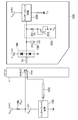
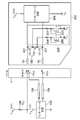
- FIG. 1 and 2 are diagrams showing the configuration of the input protection circuit according to the first embodiment of the present invention.
- reference numeral 500 denotes a device that can be inserted and removed, such as a mobile memory card.
- the external terminal Sig included in the device 500 is a signal electrode, and is electrically connected to the terminal SSig of the socket S when the socket S such as a combo socket is inserted, via the terminal SSig of the socket S and the communication path 120.
- the interface circuit 130 is connected.
- a termination device 100 having a predetermined impedance is inserted between the termination voltage Vtt and a signal node (external terminal Sig).
- a resistance element 201 and a diode element 202 are inserted. Are provided in series.
- the external terminal Sig includes an interface circuit 300 that transmits and receives signals through the external terminal Sig.
- the interface circuit 300 is an input circuit, an output circuit, or an input / output circuit.
- the interface circuit 300 should be protected from the external high voltage V DDH when it accidentally contacts the signal terminal HVBUS in the socket S pulled up to the high voltage V DDH via the resistor 150. It becomes a target.
- An ESD protection circuit 140 is connected to the external terminal Sig.
- FIG. 2 is a diagram in which the diode element 202 in FIG. 1 is specifically constituted by a MOS transistor 203 and the diode characteristics of the MOS transistor 203 are used.
- the present embodiment is suitable for mounting on a semiconductor integrated device.
- the MOS transistor 203 uses an N-type MOS transistor.
- the use of a P-type MOS transistor can provide the same effect as a diode.
- the protection circuit 200 is characterized in how to determine the resistance value of the resistance element 201.
- a voltage protection function is realized when the signal terminal HVBUS pulled up to the high voltage V DDH via the resistor 150 contacts the external terminal Sig. It is necessary to decide the parameters to do, and this will be explained.
- FIG. 3A and 3B show a configuration example of a termination device whose termination impedance is a real value
- FIG. 3C shows a configuration example of the termination device whose termination impedance is a complex value
- FIG. 3A shows a termination device using a pure resistor 101, which can terminate at a constant value over the entire frequency range
- FIG. 3B shows a termination device in which a resistor 101 and a capacitor 102 are connected in series. In the configuration of FIG.
- FIG. 3C shows a termination device in which a resistor 101 and an inductor 103 are connected in series.
- a system that matches a generally used 50 ⁇ transmission line is taken as an example, and a case where the protection circuit 200 is formed on a semiconductor integrated circuit and a MOS transistor is used as a diode element is considered.
- the power supply voltage V DD of the interface circuit 300 is standard 1.2V, minimum 1.1V, the desired termination impedance is 50 ⁇ , and the power supply voltage V DDH of the signal electrode terminal HVBUS of the socket S is standard 3.3V, maximum 3.6V.
- the power supply voltage V DDH is pulled up through a resistor 150 having a resistance value R PU of 10 k ⁇ to 100 k ⁇ , the voltage of the external terminal Sig is lowered to 1.2 V or less by the protection circuit 200.
- the following are examples of specific cases.
- the termination voltage V TT may be handled as ground when considering a small signal equivalent circuit for an AC signal, and a specific voltage value is determined by an electrical standard of the interface circuit 300.
- the threshold value of the MOS transistor 203 is maximum, the power supply voltage V DD of the interface circuit 300 is minimum, the power supply voltage V DDH of the signal electrode terminal HVBUS is maximum, and the pull-up resistor 150 This is when the resistance value R PU is initially 10 k ⁇ .
- the maximum threshold value of the MOS transistor 203 is 500 mV
- the minimum value of the power supply voltage V DD of the interface circuit 300 is 1.1 V
- the maximum value of the power supply voltage V DDH of the signal electrode terminal HVBUS is 3.6 V.
- the remaining voltage (3.6 ⁇ 0.5) V 3.1 V is set to the resistance value R of the resistance element 201 and the pull-up resistance on the socket S side.
- the resistance value is less than that.
- the impedance value is the sum of the resistance value R of the resistor 201 and the impedance of the diode element 202, but since the impedance value of the protection circuit 200 is the minimum because it is connected in parallel with the termination resistor 100. In this case, the worst condition is that the fluctuation amount given to the termination impedance characteristic is the maximum.
- the resistance value R of the resistance element 201 is fixed, while the impedance of the diode element 203 is a parallel impedance of parasitic capacitance and on-resistance.
- the worst condition is that the impedance of the protection circuit 200 is the resistance value R of the resistance element 201. Can be considered to be equal to.
- the resistance value R of the resistor element 201 is
- the resistance value R of the resistance element 201 included in the protection circuit 200 is between 450 ⁇ and 2.4 k ⁇ , and the input protection voltage margin and the allowable range of the variation width of the termination resistance characteristics, This can be determined according to design factors such as mounting area and cost factors.
- the characteristic impedance becomes a complex number, and the condition for matching the termination impedance of the termination device 100 must be a complex number equivalent to the transmission line.
- the characteristic impedance Z0 of the transmission line is
- j is an imaginary unit
- ⁇ 0 is a complex angle of Z 0 in the impedance plane
- the real component of impedance Z 0 is represented by
- the imaginary component is represented by j
- the termination impedance Z tt of the termination device 100 is
- ⁇ tt is a complex angle of the termination impedance Z tt of the termination device 100 in the impedance plane
- the real component of the impedance Z tt is represented by
- the imaginary component is represented by j
- the reflection coefficient ⁇ in the termination device 100 of the circuit in which the transmission line and the termination device 100 are connected is
- is Zr
- the step size of the ratio Zr is set to every 3%
- the step size of the phase difference ⁇ d of the complex angle is set to every 2 degrees
- this protection circuit 200 work as an ESD protection circuit, since the impedance is too high and the direction of current flow is one direction, it is not practical and the ESD protection circuit 140 needs to be provided separately. Since it is essentially different from the present invention, it is not shared.
- a separately provided ESD protection diode element is used as a countermeasure for this problem, the forward current continuously flows into the power supply side protection diode, the driver circuit of the interface circuit, etc., which may promote deterioration of device characteristics. There is.
- the external terminal converges to a voltage obtained by adding the threshold voltage of the ESD protection diode to the power supply voltage. Therefore, the PMOS transistor constituting the interface circuit whose gate terminal is connected to the external terminal is PBTI. There is a possibility that the characteristic variation is accelerated due to the deterioration condition. Therefore, it is desirable to avoid such implementation from the viewpoint of reliability.
- the protection circuit 200 can obtain the same effect when connected to the differential signal terminal of the differential interface.
- 5 and 6 are diagrams showing a configuration of a modification in which the protection circuit according to the first embodiment is applied to a differential interface circuit.
- a termination resistor 100 of 20 ⁇ to 400 ⁇ is connected between the differential signal terminal pair Sig + and Sig ⁇ of the differential interface circuit 400.
- a resistance element 201 and a diode element 202 are connected in series to one terminal Sig + of the differential signal terminal pair, and a resistance element 204 and a diode element 2052 are connected in series to the other terminal Sig ⁇ .
- a protection circuit 200 is configured.
- the power supply voltage V DDH of the signal electrode terminal HVBUS of the socket S is typically 3.3 V and a maximum of 3.6 V, and may be pulled up via a pull-up resistor 150 of 5 k ⁇ to 500 k ⁇ with respect to the power supply voltage V DDH If there is a possibility, the same effect can be obtained even when only one of the differential signal terminal pair Sig + and Sig + is connected. Of course, the effect is the same even if it is connected to both of the differential signal terminal pair Sig + and Sig ⁇ .
- one signal terminal HVBUS pulled up to the high voltage V DDH via the resistor 100 is arranged close to the signal terminal SSig +.
- the present invention can be similarly applied to the case where the signal terminal HVBUS (not shown) pulled up to the high voltage V DDH is disposed close to the signal terminal Sig ⁇ .
- all of the embodiments shown in FIGS. 1, 2, 5 and 6 perform a protection operation in response to only the high voltage V DDH applied to the external terminal Sig (or Sig +, Sig ⁇ ). Since it does not depend on the operation state of the interface circuits 300 and 400, hot-line insertion / removal is frequently performed as in the case where the interface circuits 300 and 400 are mobile memory cards, and before the internal state is determined, the external terminal Sig (Or Sig +, Sig ⁇ ) has the added advantage of being more suitable to be applied to a device where a high voltage V DDH may be applied.
- the diode element 202 when a diode element composed only of a PN junction is used as the diode element 202, it is clear that the effect is the same even if the connection between the resistance element 201 and the diode element 202 is switched. is there. Further, when a MOS transistor is used as the diode element 202, the effect as the protection circuit 200 can be similarly obtained even if the resistance element 201 and the diode element 202 are interchanged. However, in this case, since the drain-substrate junction capacitance of the MOS transistor is added to the input capacitance, it is necessary to consider that the influence on the termination impedance characteristic changes.
- FIG. 7 shows a configuration of an input protection circuit according to the second embodiment of the present invention.
- the configuration in which the MOS transistor diode element 203 is arranged is replaced with a source voltage follower circuit including the NMOS transistor 207 and the differential amplifier 208 in FIG.
- the output of the differential amplifier 208 is connected to the gate terminal of the NMOS transistor 207
- the drain terminal of the NMOS transistor 207 is connected to the non-inverting input of the differential amplifier 208
- the inverting input of the differential amplifier 208 Is supplied with the reference voltage ref generated by the reference voltage generation circuit VG1.
- the differential amplifier 208 starts an operation of raising the gate of the NMOS transistor 207.
- the NMOS transistor 207 is turned on, the NMOS transistor 207 starts to reduce its drain terminal voltage, and the drain voltage of the NMOS transistor 207 is stabilized near the reference voltage ref.
- the threshold voltage of the NMOS transistor 207 can be accurately determined by the differential amplifier 208 and the reference voltage generation circuit VG1, so that there is an advantage that the design can be performed without worrying about variations in the threshold voltage.
- the resistance value R of the resistance element 201 included in the protection circuit 200 can be determined by the same method as that of the first embodiment only by replacing the threshold value of the diode element with the reference voltage ref. Further, the variation amount of the reflection coefficient ⁇ when the termination impedance of the termination device 100 is a complex number can be calculated in the same manner as in the first embodiment.
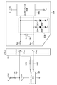
- (Embodiment 3) 8 and 9 are diagrams showing the configuration of the input protection circuit according to the third embodiment of the present invention.
- reference numeral 500 denotes a device that employs a differential interface in which a termination device 104 is connected between a differential signal terminal pair Sig + and Sig ⁇ , which can be inserted and removed from a mobile memory card or the like.
- the differential signal terminal pair Sig +, Sig ⁇ included in the device 500 is an external terminal electrode and is electrically connected to the differential signal electrodes SSig +, SSig ⁇ included in the socket S.
- a termination device 104 having a predetermined impedance is inserted between the differential signal terminal pair Sig +, Sig ⁇ , and an intermediate node TC in which the impedance value of the termination device 100 is 1 ⁇ 2.
- a protection circuit 200 is provided which is connected in series with a resistance element 201 and a diode element 202 having an anode connected to the resistance element 201 and a cathode connected to a reference potential.
- the differential signal terminal pair Sig +, Sig ⁇ has a differential interface circuit 400 to be protected from an external voltage.
- the differential interface circuit 400 is an input circuit, an output circuit, or an input / output circuit.
- FIG. 9 shows a diagram in which the diode element 202 of FIG. 8 is specifically composed of a MOS transistor diode element 203.
- the MOS transistor diode element 203 has a drain terminal and a gate terminal connected to serve as an anode terminal and a source terminal as a cathode terminal, and utilizes the diode characteristics.
- the resistance value R of the resistance element 201 of the protection circuit 200 is a voltage when the signal terminal HVBUS of the socket S pulled up to the high voltage V DDH through the high resistance 150 contacts the signal terminal Sig +. What is necessary is just to determine the parameter for implement
- the calculation method of the resistance value R is that the DC impedance value of the termination device Z tt , that is, the half value (R tt / 2) of the real component R tt is added to the resistance value R of the resistance element 201 of the protection circuit 200.
- the voltage division ratio is ⁇ R + (R tt / 2) ⁇ / ⁇ R PU + (R + R tt / 2) ⁇ , it can be determined in the same manner as in the first embodiment.
- the impedance intermediate node TC of the termination device 104 corresponds to a common voltage point. That is, in the small signal equivalent circuit when a differential signal is inputted to the differential signal terminal pair Sig +, Sig ⁇ , as shown in FIG. 10, the impedance intermediate node TC becomes a ground node. Therefore, even if a circuit having any impedance value is inserted between the intermediate node TC and the ground potential, the combined impedance with respect to the AC signal component becomes 0, and the waveform quality of the signal is not affected.
- the impedance intermediate node TC is in a state where a common voltage is applied as DC when transmitting and receiving a low-amplitude signal.
- the common voltage Vcm is a high potential level Vih or an output of the input signal. It is always lower than the value of the high potential level Voh of the signal.
- the fluctuation range of the signal potential is 1 ⁇ 2 of the fluctuation range of the signal amplitude to the fluctuation range of the common potential Vcm, the fluctuation of the common potential Vcm is relatively larger than the fluctuation range of the signal potential. The width becomes smaller.
- the high potential level Vih or output of the input signal as in the first and third embodiments shown in FIGS.
- the protection circuit 20 is turned on in a voltage range exceeding the value of the high potential level Voh of the signal, in this method, the on region of the diode element 202 of the protection circuit 200 is the common region as shown in FIG. Since the voltage range exceeds the potential Vcm, the effect that the protection circuit 200 becomes difficult to enter the operation region during differential signal transmission is obtained, and this is a suitable method that can maximize the design margin.
- the protection circuit 200 performs a protection operation only in response to a high voltage applied to the external terminals Sig + and Sig ⁇ , and does not depend on the operation state of the interface circuit 400.
- the advantage is that it is more suitable to be applied to a device such as a mobile memory card where hot plugging is frequently performed and a high voltage may be applied to the external terminal before the internal state is determined. is there.
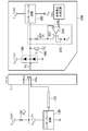
- (Embodiment 4) 12 and 13 show the configuration of the input protection circuit according to the fourth embodiment of the present invention.
- reference numeral 500 includes a termination device 100 in which two termination circuits 107 that can be inserted into and removed from a mobile memory card or the like and are in charge of 1/2 each termination impedance between the differential signal terminal pair Sig + and Sig ⁇ are connected in series.
- the impedance intermediate point of the termination device 100 includes a connection switch 105 for switching the termination device 100 between the differential signal terminal pair Sig + and Sig ⁇ to a connected state / non-connected state, and a differential interface circuit 400. It is a device equipped with.
- connection switch 105 is ON / OFF controlled according to the unidirectional / bidirectional communication mode of the device 500 and the like.
- the differential signal terminal pair Sig +, Sig ⁇ of the device 500 is electrically connected to the differential signal terminal pair SSig +, SSig ⁇ of the socket S.
- a resistance element 201 and a diode element 202 are connected in series to one end of the connection switch 105, and another resistance element 204 and a diode element 205 are connected in series to the other end of the connection switch 105 for protection.
- a circuit 200 is configured.
- FIG. 13 shows a diagram in which the diode elements 202 and 205 in FIG. 12 are specifically composed of MOS transistor diode elements 203 and 206.
- MOS transistor diode elements 203 and 205 the drain terminal and the gate terminal are connected to serve as an anode terminal, the source terminal is used as the cathode terminal, and the diode characteristics are used.
- an N-type MOS transistor is used as a diode element.
- a P-type MOS transistor is used, the same effect as a diode element can be obtained.
- the protection circuit 200 performs a protection operation only in response to a high voltage applied to the external terminals Sig + and Sig ⁇ , and the connection switch 105 that is the operation state of the interface circuit 400 is in an ON / OFF state. Therefore, there is a possibility that a high voltage is applied to the external terminal before the internal state is determined by frequent hot-swap as in the case where the interface circuit 400 is a mobile memory card. It has the advantage of being more suitable to apply to.
- the protection circuit according to the present invention can be designed with a digital transistor.
- a semiconductor integrated circuit it can be realized with a small circuit configuration without adding external parts, and the termination impedance is guaranteed. For example, it is useful for application to a mobile memory card interface circuit that is frequently inserted into a combo socket of a personal computer.
- Termination circuit 100, 104 Termination device 101 Pure resistance 102 Capacitance 103 Inductor 105 Connection switch 107 Termination circuit 120 Communication path 130 Interface circuit 140 ESD protection circuit 150 Pull-up resistor 200 Protection circuit 201, 204 Resistance element 202, 205 Diode element 203, 206 MOS transistor 207 N-type MOS transistor 208 differential amplifier 300 interface circuit 400 differential interface circuit VSS reference potential terminal V DD interface circuit power supply V DDH high voltage power supply S socket Sig, Sig +, Sig- outer Terminal SSig, SSig +, SSig- socket side of the signal terminals HVBUS signal terminal
Landscapes
- Engineering & Computer Science (AREA)
- Computer Hardware Design (AREA)
- Physics & Mathematics (AREA)
- Computing Systems (AREA)
- General Engineering & Computer Science (AREA)
- Mathematical Physics (AREA)
- Logic Circuits (AREA)
- Semiconductor Integrated Circuits (AREA)
Abstract
L'invention concerne un circuit de protection d'entrée, dans lequel une extrémité d'une résistance (201) d'un circuit de protection (200) est connectée à un point central d'impédance (TC) d'un dispositif de terminaison (100) qui est connecté entre une paire de bornes extérieures (Sig+, Sig-) d'un circuit d'interface différentiel à faible amplitude (400) et l'autre extrémité de la résistance (201) est connectée à une borne d'anode d'un élément à diode (203), la borne de cathode de l'élément à diode (203) étant connectée à une borne de potentiel de référence (VSS). Cette configuration assure une bonne protection à faible coût contre la dégradation ou la destruction, etc., des éléments composant le circuit, tout en maintenant la qualité des signaux transmis, lorsque les bornes extérieures (Sig+, Sig-) d'un circuit de tension à faible résistance entrent par erreur en contact avec une borne de signal (une borne de bus qui est constamment élevée par une résistance élevée) (HVBUS) d'une douille (S) et sont portées à une haute tension (VDDH).
Priority Applications (2)
| Application Number | Priority Date | Filing Date | Title |
|---|---|---|---|
| JP2013500677A JPWO2012114392A1 (ja) | 2011-02-25 | 2011-07-26 | 入力保護回路 |
| US13/975,041 US20130342943A1 (en) | 2011-02-25 | 2013-08-23 | Input protection circuit |
Applications Claiming Priority (2)
| Application Number | Priority Date | Filing Date | Title |
|---|---|---|---|
| JP2011040329 | 2011-02-25 | ||
| JP2011-040329 | 2011-02-25 |
Related Child Applications (1)
| Application Number | Title | Priority Date | Filing Date |
|---|---|---|---|
| US13/975,041 Continuation US20130342943A1 (en) | 2011-02-25 | 2013-08-23 | Input protection circuit |
Publications (1)
| Publication Number | Publication Date |
|---|---|
| WO2012114392A1 true WO2012114392A1 (fr) | 2012-08-30 |
Family
ID=46720215
Family Applications (1)
| Application Number | Title | Priority Date | Filing Date |
|---|---|---|---|
| PCT/JP2011/004197 Ceased WO2012114392A1 (fr) | 2011-02-25 | 2011-07-26 | Circuit de protection d'entrée |
Country Status (3)
| Country | Link |
|---|---|
| US (1) | US20130342943A1 (fr) |
| JP (1) | JPWO2012114392A1 (fr) |
| WO (1) | WO2012114392A1 (fr) |
Cited By (3)
| Publication number | Priority date | Publication date | Assignee | Title |
|---|---|---|---|---|
| CN103713678A (zh) * | 2012-09-28 | 2014-04-09 | 富士通半导体股份有限公司 | 保护电路、接口电路及通信系统 |
| JP2014144699A (ja) * | 2013-01-29 | 2014-08-14 | Sanyo Electric Co Ltd | 電動自転車及び充電器、回路 |
| WO2025192151A1 (fr) * | 2024-03-13 | 2025-09-18 | ソニーセミコンダクタソリューションズ株式会社 | Dispositif de circuit |
Families Citing this family (4)
| Publication number | Priority date | Publication date | Assignee | Title |
|---|---|---|---|---|
| CN109066577B (zh) * | 2018-09-14 | 2024-02-20 | 深圳众城卓越科技有限公司 | 一种抱闸驱动电路 |
| US11043488B2 (en) * | 2019-01-24 | 2021-06-22 | Western Digital Technologies, Inc. | High voltage protection for high-speed data interface |
| US11137932B2 (en) * | 2019-12-02 | 2021-10-05 | Western Digital Technologies, Inc. | Pad indication for device capability |
| CN111141962B (zh) * | 2020-01-19 | 2024-05-24 | 湖南大学 | 一种测量功率器件c-v曲线的测量电路及其保护方法 |
Citations (4)
| Publication number | Priority date | Publication date | Assignee | Title |
|---|---|---|---|---|
| JP2002344303A (ja) * | 2001-05-18 | 2002-11-29 | Mitsubishi Electric Corp | レベルシフト回路 |
| JP2006202979A (ja) * | 2005-01-20 | 2006-08-03 | Hitachi Ltd | 半導体装置 |
| JP2010211645A (ja) * | 2009-03-11 | 2010-09-24 | Ricoh Co Ltd | 電子装置 |
| JP2010233140A (ja) * | 2009-03-30 | 2010-10-14 | Hitachi Ltd | 半導体集積回路装置 |
Family Cites Families (6)
| Publication number | Priority date | Publication date | Assignee | Title |
|---|---|---|---|---|
| US3982233A (en) * | 1974-02-19 | 1976-09-21 | Ampex Corporation | Core memory with improved sense-inhibit recovery time |
| US6323756B1 (en) * | 1997-09-02 | 2001-11-27 | Matsushita Electric Industrial Co., Ltd. | Data transmitter |
| US6650280B2 (en) * | 2000-12-08 | 2003-11-18 | The United States Of America As Represented By The Administrator Of The National Aeronautics And Space Administration | Measurement system and method |
| DE102004017284B4 (de) * | 2004-04-07 | 2012-06-06 | Qimonda Ag | Integrierte Halbleiterschaltung und Verfahren zur Prüfung der integrierten Halbleiterschaltung |
| JP4544326B2 (ja) * | 2008-03-26 | 2010-09-15 | セイコーエプソン株式会社 | 集積回路装置、電気光学装置及び電子機器 |
| TWI453893B (zh) * | 2011-08-15 | 2014-09-21 | Faraday Tech Corp | 靜電放電保護電路 |
-
2011
- 2011-07-26 JP JP2013500677A patent/JPWO2012114392A1/ja not_active Withdrawn
- 2011-07-26 WO PCT/JP2011/004197 patent/WO2012114392A1/fr not_active Ceased
-
2013
- 2013-08-23 US US13/975,041 patent/US20130342943A1/en not_active Abandoned
Patent Citations (4)
| Publication number | Priority date | Publication date | Assignee | Title |
|---|---|---|---|---|
| JP2002344303A (ja) * | 2001-05-18 | 2002-11-29 | Mitsubishi Electric Corp | レベルシフト回路 |
| JP2006202979A (ja) * | 2005-01-20 | 2006-08-03 | Hitachi Ltd | 半導体装置 |
| JP2010211645A (ja) * | 2009-03-11 | 2010-09-24 | Ricoh Co Ltd | 電子装置 |
| JP2010233140A (ja) * | 2009-03-30 | 2010-10-14 | Hitachi Ltd | 半導体集積回路装置 |
Cited By (5)
| Publication number | Priority date | Publication date | Assignee | Title |
|---|---|---|---|---|
| CN103713678A (zh) * | 2012-09-28 | 2014-04-09 | 富士通半导体股份有限公司 | 保护电路、接口电路及通信系统 |
| CN103713678B (zh) * | 2012-09-28 | 2016-04-27 | 株式会社索思未来 | 保护电路、接口电路及通信系统 |
| US9520708B2 (en) | 2012-09-28 | 2016-12-13 | Socionext Inc. | Protection circuit, interface circuit, and communication system |
| JP2014144699A (ja) * | 2013-01-29 | 2014-08-14 | Sanyo Electric Co Ltd | 電動自転車及び充電器、回路 |
| WO2025192151A1 (fr) * | 2024-03-13 | 2025-09-18 | ソニーセミコンダクタソリューションズ株式会社 | Dispositif de circuit |
Also Published As
| Publication number | Publication date |
|---|---|
| US20130342943A1 (en) | 2013-12-26 |
| JPWO2012114392A1 (ja) | 2014-07-07 |
Similar Documents
| Publication | Publication Date | Title |
|---|---|---|
| US11848552B2 (en) | USB type-C/PD controller having integrated VBUS to CC short protection | |
| US10148084B2 (en) | Overvoltage protection circuit for USB interface | |
| WO2012114392A1 (fr) | Circuit de protection d'entrée | |
| US10990560B2 (en) | USB type-C sideband signal interface circuit | |
| EP2526618B1 (fr) | Circuit de protection contre les décharges électrostatiques haute tension et haute fréquence pour les circuits intégrés rf | |
| CN102904235B (zh) | 以太网络受电电路与其静电防护电路 | |
| CN108666303B (zh) | 用于电过应力和静电放电保护的方法和器件 | |
| US20130194005A1 (en) | Generation of differential signals | |
| US9209799B2 (en) | Switch and switch circuit using the same | |
| US20200264643A1 (en) | Controller area network (can) transceiver | |
| US9391602B1 (en) | Differential driver circuit and method for controlling a differential driver circuit | |
| JP2008028214A (ja) | 静電気対策回路 | |
| CN101944901B (zh) | 包括宽带高压缓冲器的集成电路 | |
| EP3471230B1 (fr) | Circuit de protection d'interface et interface de dispositif | |
| US12483445B2 (en) | Differential transmitter circuitry with ESD circuitry | |
| US20250192546A1 (en) | Communication circuit having a termination resistance circuit with esd circuitry | |
| CN120033639A (zh) | Esd保护电路、半导体芯片、基站和移动设备 | |
| CN107395192A (zh) | 双向接口电路 | |
| CN107437894B (zh) | 过电压保护装置 | |
| US8559145B1 (en) | Serializer/deserializer frontend | |
| CN2750618Y (zh) | 一种usb接口的静电放电保护结构 | |
| US11909388B2 (en) | Terminal resistance circuit, chip and chip communication device | |
| US9628069B2 (en) | Transmission circuit with leakage prevention circuit | |
| CN102692539A (zh) | 过压容限电平检测电路、其操作方法及系统 | |
| CN120074483A (zh) | 开关电路、衰减电路、接收机、基站和移动设备 |
Legal Events
| Date | Code | Title | Description |
|---|---|---|---|
| 121 | Ep: the epo has been informed by wipo that ep was designated in this application |
Ref document number: 11859208 Country of ref document: EP Kind code of ref document: A1 |
|
| ENP | Entry into the national phase |
Ref document number: 2013500677 Country of ref document: JP Kind code of ref document: A |
|
| NENP | Non-entry into the national phase |
Ref country code: DE |
|
| 122 | Ep: pct application non-entry in european phase |
Ref document number: 11859208 Country of ref document: EP Kind code of ref document: A1 |