WO2012114701A1 - ディスプレイ装置の製造方法 - Google Patents
ディスプレイ装置の製造方法 Download PDFInfo
- Publication number
- WO2012114701A1 WO2012114701A1 PCT/JP2012/001087 JP2012001087W WO2012114701A1 WO 2012114701 A1 WO2012114701 A1 WO 2012114701A1 JP 2012001087 W JP2012001087 W JP 2012001087W WO 2012114701 A1 WO2012114701 A1 WO 2012114701A1
- Authority
- WO
- WIPO (PCT)
- Prior art keywords
- display panel
- flat display
- liquid crystal
- circuit board
- crystal display
- Prior art date
- Legal status (The legal status is an assumption and is not a legal conclusion. Google has not performed a legal analysis and makes no representation as to the accuracy of the status listed.)
- Ceased
Links
Images




Classifications
-
- H—ELECTRICITY
- H05—ELECTRIC TECHNIQUES NOT OTHERWISE PROVIDED FOR
- H05K—PRINTED CIRCUITS; CASINGS OR CONSTRUCTIONAL DETAILS OF ELECTRIC APPARATUS; MANUFACTURE OF ASSEMBLAGES OF ELECTRICAL COMPONENTS
- H05K13/00—Apparatus or processes specially adapted for manufacturing or adjusting assemblages of electric components
-
- G—PHYSICS
- G02—OPTICS
- G02F—OPTICAL DEVICES OR ARRANGEMENTS FOR THE CONTROL OF LIGHT BY MODIFICATION OF THE OPTICAL PROPERTIES OF THE MEDIA OF THE ELEMENTS INVOLVED THEREIN; NON-LINEAR OPTICS; FREQUENCY-CHANGING OF LIGHT; OPTICAL LOGIC ELEMENTS; OPTICAL ANALOGUE/DIGITAL CONVERTERS
- G02F1/00—Devices or arrangements for the control of the intensity, colour, phase, polarisation or direction of light arriving from an independent light source, e.g. switching, gating or modulating; Non-linear optics
- G02F1/01—Devices or arrangements for the control of the intensity, colour, phase, polarisation or direction of light arriving from an independent light source, e.g. switching, gating or modulating; Non-linear optics for the control of the intensity, phase, polarisation or colour
- G02F1/13—Devices or arrangements for the control of the intensity, colour, phase, polarisation or direction of light arriving from an independent light source, e.g. switching, gating or modulating; Non-linear optics for the control of the intensity, phase, polarisation or colour based on liquid crystals, e.g. single liquid crystal display cells
- G02F1/133—Constructional arrangements; Operation of liquid crystal cells; Circuit arrangements
- G02F1/1333—Constructional arrangements; Manufacturing methods
- G02F1/133308—Support structures for LCD panels, e.g. frames or bezels
-
- H—ELECTRICITY
- H04—ELECTRIC COMMUNICATION TECHNIQUE
- H04N—PICTORIAL COMMUNICATION, e.g. TELEVISION
- H04N5/00—Details of television systems
- H04N5/64—Constructional details of receivers, e.g. cabinets or dust covers
-
- G—PHYSICS
- G02—OPTICS
- G02F—OPTICAL DEVICES OR ARRANGEMENTS FOR THE CONTROL OF LIGHT BY MODIFICATION OF THE OPTICAL PROPERTIES OF THE MEDIA OF THE ELEMENTS INVOLVED THEREIN; NON-LINEAR OPTICS; FREQUENCY-CHANGING OF LIGHT; OPTICAL LOGIC ELEMENTS; OPTICAL ANALOGUE/DIGITAL CONVERTERS
- G02F1/00—Devices or arrangements for the control of the intensity, colour, phase, polarisation or direction of light arriving from an independent light source, e.g. switching, gating or modulating; Non-linear optics
- G02F1/01—Devices or arrangements for the control of the intensity, colour, phase, polarisation or direction of light arriving from an independent light source, e.g. switching, gating or modulating; Non-linear optics for the control of the intensity, phase, polarisation or colour
- G02F1/13—Devices or arrangements for the control of the intensity, colour, phase, polarisation or direction of light arriving from an independent light source, e.g. switching, gating or modulating; Non-linear optics for the control of the intensity, phase, polarisation or colour based on liquid crystals, e.g. single liquid crystal display cells
- G02F1/133—Constructional arrangements; Operation of liquid crystal cells; Circuit arrangements
- G02F1/1333—Constructional arrangements; Manufacturing methods
- G02F1/133308—Support structures for LCD panels, e.g. frames or bezels
- G02F1/133325—Assembling processes
-
- G—PHYSICS
- G02—OPTICS
- G02F—OPTICAL DEVICES OR ARRANGEMENTS FOR THE CONTROL OF LIGHT BY MODIFICATION OF THE OPTICAL PROPERTIES OF THE MEDIA OF THE ELEMENTS INVOLVED THEREIN; NON-LINEAR OPTICS; FREQUENCY-CHANGING OF LIGHT; OPTICAL LOGIC ELEMENTS; OPTICAL ANALOGUE/DIGITAL CONVERTERS
- G02F2201/00—Constructional arrangements not provided for in groups G02F1/00 - G02F7/00
- G02F2201/46—Fixing elements
-
- H—ELECTRICITY
- H04—ELECTRIC COMMUNICATION TECHNIQUE
- H04N—PICTORIAL COMMUNICATION, e.g. TELEVISION
- H04N5/00—Details of television systems
- H04N5/64—Constructional details of receivers, e.g. cabinets or dust covers
- H04N5/642—Disposition of sound reproducers
-
- Y—GENERAL TAGGING OF NEW TECHNOLOGICAL DEVELOPMENTS; GENERAL TAGGING OF CROSS-SECTIONAL TECHNOLOGIES SPANNING OVER SEVERAL SECTIONS OF THE IPC; TECHNICAL SUBJECTS COVERED BY FORMER USPC CROSS-REFERENCE ART COLLECTIONS [XRACs] AND DIGESTS
- Y10—TECHNICAL SUBJECTS COVERED BY FORMER USPC
- Y10T—TECHNICAL SUBJECTS COVERED BY FORMER US CLASSIFICATION
- Y10T29/00—Metal working
- Y10T29/49—Method of mechanical manufacture
- Y10T29/49002—Electrical device making
Definitions
- the present invention relates to a method of manufacturing a display device such as a liquid crystal display device used in a television receiver or a monitor device.
- a liquid crystal display device includes a display module formed by arranging a backlight device as a surface light source on the back side of a flat liquid crystal display panel.
- the display module is housed in a thin housing having a front cabinet and a back cabinet (see Patent Document 1).
- the liquid crystal display device is completed as follows, for example. Panel manufacturers manufacture LCD panels and deliver them to finished product manufacturers such as TV manufacturers. A finished product manufacturer produces a display module by combining a liquid crystal display panel and a backlight device as a surface light source. The display module is housed in a thin casing having a front cabinet and a back cabinet together with a driving circuit board of the liquid crystal display panel. In this way, a liquid crystal display device is completed.
- the finished product manufacturer builds a factory for assembling products in the region where the liquid crystal display device is sold or is close to that region, and assembles the finished product with the design and functions corresponding to the selling region. I am trying to sell.
- the present invention relates to a housing having a back cabinet, a flat display panel installed in the housing, a backlight device disposed on the back side of the flat display panel, and an image on the flat display panel.
- a circuit board constituting a drive circuit for displaying an image on a backlight device, a flat display panel, and a flat display panel A space that can accommodate the board is provided, and the backlight device and the circuit board are accommodated and mounted in the back cabinet, and a dummy panel having the same shape as the flat display panel is arranged at the position for accommodating the flat display panel. Then packed and transported.
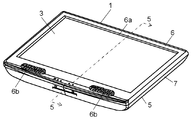
- FIG. 1 is a front view showing an appearance of a liquid crystal display device in an embodiment of the present invention.
- FIG. 2 is a perspective view showing the liquid crystal display device with the stand removed.
- FIG. 3 is a block diagram showing a circuit block of the entire configuration of the liquid crystal display device.
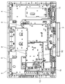
- FIG. 4 is a plan view showing a state in which the back cabinet is removed in order to explain an arrangement example of circuit blocks of the liquid crystal display device.
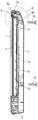
- FIG. 5 is a cross-sectional view showing the liquid crystal display device taken along line 5-5 in FIG.
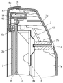
- FIG. 6 is an enlarged view showing a portion B of FIG.
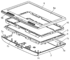
- FIG. 7 is an exploded perspective view showing each part of the liquid crystal display device.
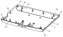
- FIG. 8 is a perspective view showing the inner wall surface of the back cabinet of the liquid crystal display device.
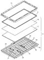
- FIG. 9 is a perspective view showing an exploded state of the backlight device of the liquid crystal display device.
- FIG. 10A is an explanatory diagram for explaining a display device manufacturing method according to the present invention.
- FIG. 10B is an explanatory diagram for explaining a display device manufacturing method according to the present invention.
- FIG. 10C is an explanatory diagram for explaining a method of manufacturing a display device according to the present invention.
- FIG. 1 is a front view showing the appearance of a liquid crystal display device according to an embodiment of the present invention
- FIG. 2 is a perspective view showing a state in which the stand is removed from the liquid crystal display device
- FIG. 3 is the entire liquid crystal display device.
- FIG. 4 is a plan view showing a state in which the back cabinet is removed for explaining an arrangement example of the circuit block of the liquid crystal display device
- FIG. 5 is a plan view showing the liquid crystal display device shown in FIG.
- FIG. 6 is an enlarged view showing a portion B of FIG. 5 in an enlarged manner
- FIG. 7 is an exploded perspective view showing each portion of the liquid crystal display device.
- the liquid crystal display device includes a display device body 1 and a stand 2 that holds the display device body 1 in a standing state.
- the display device body 1 is configured by housing a display module including a liquid crystal display panel 3 which is a flat display panel and a backlight device 4 (shown in FIG. 5) in a housing 5 made of a resin molded product.
- the housing 5 includes a front cabinet 6 provided with an opening 6 a so as to correspond to an image display area of the liquid crystal display panel 3, and a back cabinet 7 combined with the front cabinet 6.
- Reference numeral 6b denotes a speaker grill for releasing the sound of the speaker to the outside.
- the schematic configuration of the entire liquid crystal display device includes a drive circuit that displays an image on the liquid crystal display panel 3. Further, a signal processing circuit block 8 having a lighting control circuit for controlling lighting of the backlight device 4, and a power supply block 9 for supplying a power supply voltage to the liquid crystal display panel 3, the backlight device 4 and the signal processing circuit block 8. And a tuner 10 for receiving a television broadcast and supplying a received signal to the signal processing circuit block 8 and a speaker 11 for outputting sound.
- the signal processing circuit block 8 and the power supply block 9 are each configured by mounting components constituting a circuit on a circuit board.
- the circuit board on which the signal processing circuit block 8, the power supply block 9, the tuner 10, and the like are mounted is attached so as to be disposed in a space between the back surface of the backlight device 4 and the back cabinet 7.
- reference numeral 12 denotes an external signal input terminal for inputting a video signal from an external device such as a DVD player to the liquid crystal display device, which is mounted on the signal processing circuit block 8.
- the back cabinet 7 is a space portion 7a that can accommodate a display module including the liquid crystal display panel 3 and the backlight device 4, and a circuit board.
- backlight support portions 7 b and 7 c that support the backlight device 4 are provided on the inner bottom surface that forms the space portion 7 a.
- a frame 4 a of the backlight device 4 is attached to the backlight support portions 7 b and 7 c with screws 13.
- a panel support portion 7 d for holding a panel support member 14 made of a resin molded product that supports the outer peripheral edge portion of the liquid crystal display panel 3 is provided on the peripheral edge portion of the inner bottom surface of the back cabinet 7.
- the metal frame 15 having a substantially L-shaped cross section.
- the liquid crystal display panel 3 is accommodated and arranged at the periphery of the opening of the space 7 a of the back cabinet 7.
- 3a is a deflection film affixed on the display surface of the liquid crystal display panel 3.
- the liquid crystal display panel 3 disposed in the opening of the space portion 7 a of the back cabinet 7 extends along the outer periphery of the backlight device 4 on the circuit board constituting the drive circuit disposed on the back side of the backlight device 4. It is electrically connected through a flexible wiring plate (not shown) arranged as described above.
- the back cabinet 7 has its outer peripheral tip 7 e fitted into a fitting piece 6 c provided on the inner peripheral wall surface of the front cabinet 6. Further, the front cabinet 6 is attached to the back cabinet 7 with screws from the front cabinet 6 side, thereby constituting a housing for accommodating a circuit board on which a display module and a drive circuit are mounted.
- FIG. 8 shows an inner wall surface of the back cabinet 7, and the front cabinet 6 is attached to the boss portion 7 f provided on the outer peripheral portion of the back cabinet 7 with screws.
- FIG. 9 is a perspective view showing an exploded state of the backlight device of the liquid crystal display device.
- the backlight device 4 illuminates the liquid crystal display panel 3 from the back side.
- a plurality of linear light sources 16 arranged so as to be parallel to the liquid crystal display panel 3 in the frame 4a and a diffusion plate 17 arranged so as to cover the frame 4a are provided.
- an optical sheet 18 such as a prism sheet that diffuses or collects light transmitted through the diffusion plate 17 is laminated.
- a reflection sheet 19 made of a metal foil or the like that reflects light emitted from the linear light source 16 toward the diffusion plate 17 is disposed on the inner bottom surface of the frame 4a so as to cover substantially the entire surface.
- a pair of support members 20 for holding the linear light source 16 are disposed apart from each other in the extending direction of 16.
- a straight tubular cold cathode fluorescent lamp (CCFL) is used as the linear light source 16, and these are arranged in parallel to each other. Both ends of the linear light source 16 are covered with the support member 20.
- the frame 4a is made of a metal such as aluminum or a resin and has a box shape that opens in one direction.
- the box-shaped frame 4a has a bottom wall that forms a bottom surface parallel to the arrangement surface of the linear light sources 16, and a side wall that rises from the peripheral edge of the bottom wall.
- a plurality of diffusion plate support members 21 that support the diffusion plate 17 are arranged on the inner bottom surface of the frame 4a.
- the diffusion plate 17 is disposed between the linear light source 16 and the liquid crystal display panel 3, and diffuses light incident from the incident surface on the linear light source 16 side and emits it from the output surface on the liquid crystal display panel 3 side. It is.
- the diffusion plate 17 is formed by injection molding of a transparent resin such as polystyrene or polycarbonate. Specifically, as shown in FIG. 9, the diffusion plate 17 is disposed on the opposite side of the reflection sheet 19 with the linear light source 16 interposed therebetween. Moreover, it has the incident surface which injects the direct light from the linear light source 16, and the reflected light from the reflective sheet 19, and the output surface which radiate
- the optical sheet 18 described above is laminated on the exit surface.
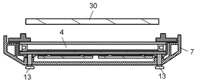
- 10A to 10C are explanatory views for explaining a method of manufacturing a display device according to the present invention.
- the display device can accommodate the backlight device 4, the liquid crystal display panel 3, and the circuit board constituting the drive circuit for displaying an image on the liquid crystal display panel 3 in the back cabinet 7.
- a space portion 7a is provided.
- the backlight device 4 and the circuit board are accommodated and attached in the back cabinet 7, and the position where the liquid crystal display panel 3 is accommodated is the same as the liquid crystal display panel 3 as shown in FIG. 10B.
- a dummy panel 30 made of a resin plate having a shape is arranged, and as shown in FIG. 10C, the front cabinet 6 is attached to pack the backlight device 4, the circuit board, and the housing 5.
- the liquid crystal display panel 3 can be prevented from being damaged during transportation by being separately packed and transported.
- the front cabinet 6 is removed and the dummy panel 30 attached to the back cabinet 7 in the reverse order of the procedure described in FIGS. 10A to 10C. Remove. Thereafter, the liquid crystal display panel 3 is attached in the order shown in FIGS. 10A to 10C, the electrical connection between the liquid crystal display panel 3 and the circuit board is made, and then the front cabinet 6 is attached, whereby the display device is completed.
- the dummy panel 30 may be collected after being removed and reused.
- the dummy panel 30 has the same shape as the liquid crystal display panel 3, this means that the shape is the same as a rectangular shape or a square shape. Of course, terminal portions for electrical connection of the liquid crystal display panel 3 have different shapes.
- the dummy panel 30 is preferably the same size as the liquid crystal display panel 3, but is not necessarily the same size.
- the broadcasting system preferred image quality, and design differ, and it is necessary to supply products that meet the customers in that sales area.
- a manufacturing method for packing, transporting, and assembling is adopted as in the present invention, the supply parts can be easily transported when assembling products in the sales area according to customers in the sales area. Is obtained.
- the present invention provides a casing having a back cabinet, a flat display panel installed inside the casing, a backlight device disposed on the back side of the flat display panel, and a flat display.
- a display device comprising a circuit board constituting a drive circuit for displaying an image on a panel, a backlight device, a flat display panel, and a drive circuit for displaying an image on the flat display panel are provided on the back cabinet.
- a space that can accommodate the circuit board to be configured is provided, and the backlight device and the circuit board are accommodated and attached in the back cabinet, and a dummy having the same shape as the flat display panel is provided at a position for accommodating the flat display panel.
- Panels are arranged, packed and transported. Therefore, it is possible to prevent the flat display panel from being damaged and to obtain an effect that a separate packing member is not required for packing the backlight device and the circuit board.
- the flat display panel is separately packed and transported, and when assembling the display device, the dummy panel attached to the back cabinet is removed, and then the flat display panel is attached. Therefore, with the back cabinet used for conveyance as a reference, the backlight device, the flat display panel, and the circuit board are sequentially assembled in the back cabinet, and the finished product can be assembled by attaching the front cabinet. Therefore, the effect that it becomes easy to assemble compared with the case where parts are separately packed and transported and assembled is obtained.
- the present invention is useful in obtaining a display device that can be easily assembled.
Landscapes
- Physics & Mathematics (AREA)
- Nonlinear Science (AREA)
- Engineering & Computer Science (AREA)
- Optics & Photonics (AREA)
- Crystallography & Structural Chemistry (AREA)
- General Physics & Mathematics (AREA)
- Chemical & Material Sciences (AREA)
- Mathematical Physics (AREA)
- Multimedia (AREA)
- Signal Processing (AREA)
- Manufacturing & Machinery (AREA)
- Microelectronics & Electronic Packaging (AREA)
- Devices For Indicating Variable Information By Combining Individual Elements (AREA)
- Liquid Crystal (AREA)
Abstract
本発明は、バックキャビネットを有する筐体と、この筐体の内部に設置された平面型表示パネルと、この平面型表示パネルの背面側に配置されたバックライト装置(4)と、平面型表示パネルに画像を表示するための駆動回路を構成する回路基板とを備えたディスプレイ装置において、バックキャビネット(7)に、バックライト装置(4)、回路基板が収容可能な空間部を設け、バックキャビネット(7)内に、バックライト装置(4)および回路基板を収容して取り付ける。さらに、平面型表示パネルを収容する位置に、平面型表示パネルと同一形状のダミーパネル(30)を配置して梱包して搬送するものである。 本発明により、平面型表示パネルの破損を防ぐとともに、バックライト装置や回路基板の梱包に別の梱包部材を必要としないという効果が得られる。
Description
本発明は、テレビジョン受像機やモニター装置に使用される液晶表示装置等のディスプレイ装置の製造方法に関するものである。
液晶表示装置は、平面型のディスプレイ装置として、一般家庭は勿論のこと、業務用として、需要が拡大している。
一般的に液晶表示装置は、平面型の液晶表示パネルの背面側に、面光源としてのバックライト装置を配置して形成した表示モジュールを備える。また、この表示モジュールは、フロントキャビネットとバックキャビネットを有する薄型の筐体の内部に収容されている(特許文献1参照)。
液晶表示装置は、例えば、次のようにして完成される。パネルメーカーが液晶表示パネルを製造してテレビメーカーなどの完成品メーカーに納入する。完成品メーカーは液晶表示パネルと面光源としてのバックライト装置とを組み合わせて表示モジュールを作製する。その表示モジュールは液晶表示パネルの駆動回路基板とともに、フロントキャビネットとバックキャビネットを有する薄型の筐体の内部に収容する。このようにすれば、液晶表示装置が完成する。
また、完成品メーカーは、液晶表示装置を販売する地域、またはその地域に近い地域に、製品を組み立てる工場を建設して、販売する地域に対応するデザイン、機能を備えた完成品の組立てを行い、販売するようにしている。
このような現状において、全世界において需要が拡大するに伴い、完成品として組み立てる際の組立て工数の削減および組み立て易さが求められる。また、組立てを行う工場に表示モジュールなどを輸送する場合の梱包方法の簡素化が求められている。
本発明は、バックキャビネットを有する筐体と、この筐体の内部に設置された平面型表示パネルと、この平面型表示パネルの背面側に配置されたバックライト装置と、平面型表示パネルに画像を表示するための駆動回路を構成する回路基板とを備えたディスプレイ装置において、バックキャビネットに、バックライト装置、平面型表示パネルおよび平面型表示パネルに画像を表示するための駆動回路を構成する回路基板が収容可能な空間部を設け、バックキャビネット内に、バックライト装置および回路基板を収容して取り付けるとともに、平面型表示パネルを収容する位置に、平面型表示パネルと同一形状のダミーパネルを配置して梱包して搬送するものである。
以下、本発明の一実施の形態によるディスプレイ装置の製造方法について、液晶表示装置に使用する表示モジュールを例にとって図面を参照しながら説明する。
図1は本発明の一実施の形態において、液晶表示装置の外観を示す正面図、図2は同液晶表示装置において、スタンドを取り外した状態を示す斜視図、図3は同液晶表示装置の全体構成の回路ブロックを示すブロック図、図4は同液晶表示装置の回路ブロックの配置例を説明するためにバックキャビネットを取り除いた状態を示す平面図、図5は同液晶表示装置を図2の5-5線で切断した状態を示す断面図、図6は図5のB部を拡大して示す拡大図、図7は同液晶表示装置の各部を分解して示す斜視図である。
まず、図1、図2に示すように、液晶表示装置は、表示装置本体1と、この表示装置本体1を立てた状態で保持するスタンド2とを有している。表示装置本体1は、平面型表示パネルである液晶表示パネル3とバックライト装置4(図5に図示)とからなる表示モジュールを樹脂成型品などからなる筐体5内に収容することにより構成されている。また、筐体5は、液晶表示パネル3の画像表示領域に対応するように開口部6aを設けたフロントキャビネット6と、このフロントキャビネット6と組み合わせられるバックキャビネット7とから構成されている。なお、6bはスピーカの音を外部に放出するためのスピーカグリルである。
また、図3、図4に示すように、液晶表示装置全体の概略構成は、液晶表示パネル3に画像を表示する駆動回路を備える。さらに、バックライト装置4の点灯を制御する点灯制御回路を備えた信号処理回路ブロック8と、液晶表示パネル3、バックライト装置4および信号処理回路ブロック8に電源電圧を供給するための電源ブロック9と、テレビジョン放送を受信して信号処理回路ブロック8に受信信号を供給するチューナ10と、音を出力するためのスピーカ11とから構成されている。また、信号処理回路ブロック8、電源ブロック9は、それぞれ回路基板に回路を構成する部品を搭載することにより構成されている。そして、信号処理回路ブロック8、電源ブロック9、チューナ10などを搭載した回路基板は、バックライト装置4の背面とバックキャビネット7との間の空間に配置されるように取り付けられている。
なお、図3においては、スピーカを省略して示している。また、図4において、12はDVDプレーヤーなどの外部機器からの映像信号を液晶表示装置に入力するための外部信号入力端子で、信号処理回路ブロック8に搭載されている。
ここで、図5~図7に示すように、本発明の液晶表示装置において、バックキャビネット7は、液晶表示パネル3とバックライト装置4からなる表示モジュール、および回路基板を収容可能な空間部7aを有する。また、空間部7aを形成する内底面には、バックライト装置4を支持するバックライト支持部7b、7cが設けられている。このバックライト支持部7b、7cには、バックライト装置4のフレーム4aがビス13により取り付けられている。
また、バックキャビネット7の内底面の周縁部には、液晶表示パネル3の外周縁部を支持する樹脂成型品からなるパネル支持部材14を保持するためのパネル支持部7dが設けられている。パネル支持部材14によって液晶表示パネル3の外周縁部を支持するとともに、断面形状が略L字形状の金属製のフレーム15によって液晶表示パネル3の外周縁部をパネル支持部材14に押し付けることにより、液晶表示パネル3がバックキャビネット7の空間部7aの開口部周縁部に収容配置されている。なお、3aは液晶表示パネル3の表示面に貼り付けられている偏向フィルムである。
ここで、バックキャビネット7の空間部7aの開口部に配置された液晶表示パネル3は、バックライト装置4の背面側に配置した駆動回路を構成する回路基板に、バックライト装置4の外周に沿うように配置されるフレキシブル配線版(図示せず)を介して電気的に接続されている。
さらに、図6に示すように、バックキャビネット7は、その外周先端部7eをフロントキャビネット6の内周壁面に設けた嵌め合せ片6cに嵌め合せている。また、フロントキャビネット6をバックキャビネット7に、フロントキャビネット6側からビスにより取り付けることにより、表示モジュールや駆動回路を搭載した回路基板を収容する筐体が構成されている。図8にバックキャビネット7の内壁面を示しており、バックキャビネット7の外周部に設けたボス部7fにフロントキャビネット6がビスにて取り付けられる。
図9は同液晶表示装置のバックライト装置を分解した状態を示す斜視図である。図9に示すように、バックライト装置4は、液晶表示パネル3を背面側から照明するものである。具体的には、フレーム4a内に液晶表示パネル3と平行となるように配列された複数本の線状光源16と、フレーム4aに蓋をするように配置された拡散板17とを備えている。また、拡散板17上には、拡散板17を透過した光を拡散または集光するプリズムシートなどの光学シート18が積層されている。フレーム4aの内底面には、線状光源16から発せられる光を拡散板17側に反射する金属箔などからなる反射シート19が略全面的に覆うように配設されているとともに、線状光源16の延在方向に離間して、線状光源16を保持するための一対の支持部材20が配置されている。
ここで、線状光源16としては、直管状の冷陰極蛍光ランプ(CCFL)が用いられており、これらが互いに平行に配列されている。そして、線状光源16の両端部が支持部材20で覆われている。また、フレーム4aは、アルミニウム等の金属または樹脂で構成されるとともに、一方向に開口する箱形状をしている。箱形状のフレーム4aは、線状光源16の配列面と平行な底面を構成する底壁と、この底壁の周縁部から立ち上がる側壁とを有している。さらに、フレーム4aの内底面には、拡散板17を支持する拡散板支持部材21が複数個配置されている。
拡散板17は、線状光源16と液晶表示パネル3との間に配設され、線状光源16側の入射面から入射した光を拡散して液晶表示パネル3側の出射面から出射するものである。この拡散板17は、ポリスチレンやポリカーボネートなどの透明な樹脂の射出成形により形成されている。具体的には、図9に示すように、拡散板17は、線状光源16を挟んで反射シート19と反対側に配設されている。また、線状光源16からの直射光および反射シート19からの反射光を内部に入射させる入射面と、内部で拡散した光を出射させる出射面とを有している。上述した光学シート18は出射面上に積層配置されている。
図10A~Cは本発明によるディスプレイ装置の製造方法を説明するための説明図である。
上述したように、本発明によるディスプレイ装置には、バックキャビネット7に、バックライト装置4および液晶表示パネル3および液晶表示パネル3に画像を表示するための駆動回路を構成する回路基板が収容可能な空間部7aを設けている。図10Aに示すように、バックキャビネット7内に、バックライト装置4および回路基板を収容して取り付け、液晶表示パネル3を収容する位置には、図10Bに示すように、液晶表示パネル3と同一形状の樹脂板からなるダミーパネル30を配置し、図10Cに示すように、フロントキャビネット6を取り付けることにより、バックライト装置4および回路基板および筐体5の梱包を行う。一方、液晶表示パネル3は、別に梱包して搬送することにより、輸送途中の破損などを防ぐことができる。
そして、別々に梱包して搬送した後、ディスプレイ装置の組み立てを行う際には、図10A~Cで説明した手順と逆の手順で、フロントキャビネット6を取り外し、バックキャビネット7に取り付けたダミーパネル30を取り外す。その後、図10A~Cに示す順番で、液晶表示パネル3を取り付け、液晶表示パネル3と回路基板との電気的接続を行った後、フロントキャビネット6の取り付けを行うことにより、ディスプレイ装置が完成される。なお、ダミーパネル30は、取り外した後、回収して、再利用すればよい。なお、ダミーパネル30は液晶表示パネル3と同一形状としているが、これは長方形状や正方形状というように、形状が同じ形状であるということを意味する。勿論、液晶表示パネル3の電気的接続のための端子部などについては、異なる形状となっている。また、ダミーパネル30は、液晶表示パネル3と同一寸法である方が望ましいが、必ずしも全く同じ寸法である必要はない。
販売地域によっては、放送方式や好まれる画質、デザインが異なっており、その販売地域の顧客に応じた製品を供給する必要がある。しかし、本発明のように、梱包、搬送、組立を行う製造方法を採用すれば、販売地域の顧客に応じた製品の組立を販売地域で行う際に、供給部品の搬送が容易に行えるという効果が得られる。
このように本発明は、バックキャビネットを有する筐体と、この筐体の内部に設置された平面型表示パネルと、この平面型表示パネルの背面側に配置されたバックライト装置と、平面型表示パネルに画像を表示するための駆動回路を構成する回路基板とを備えたディスプレイ装置において、バックキャビネットに、バックライト装置、平面型表示パネルおよび平面型表示パネルに画像を表示するための駆動回路を構成する回路基板が収容可能な空間部を設け、バックキャビネット内に、バックライト装置および回路基板を収容して取り付けるとともに、平面型表示パネルを収容する位置に、平面型表示パネルと同一形状のダミーパネルを配置して梱包して搬送するものである。そのため、平面型表示パネルの破損を防ぐとともに、バックライト装置や回路基板の梱包に別の梱包部材を必要としないという効果が得られる。
また、平面型表示パネルは別に梱包して搬送し、ディスプレイ装置の組み立てを行う際に、前記バックキャビネットに取り付けたダミーパネルを取り外し、その後平面型表示パネルを取り付ける。そのため、搬送に使用したバックキャビネットを基準として、バックキャビネット内にバックライト装置、平面型表示パネル、回路基板を順次組み込むとともに、フロントキャビネットを取り付けることにより、完成品の組立てを行うことができる。したがって、別々に部品を梱包して搬送し、そして組み立てを行う場合に比べ、組み立て易くなるという効果が得られる。
以上のように本発明によれば、組立ての容易なディスプレイ装置を得る上で有用である。
1 表示装置本体
3 液晶表示パネル
4 バックライト装置
5 筐体
6 フロントキャビネット
7 バックキャビネット
7a 空間部
7b,7c バックライト支持部
7d パネル支持部
14 パネル支持部材
15 フレーム
30 ダミーパネル
3 液晶表示パネル
4 バックライト装置
5 筐体
6 フロントキャビネット
7 バックキャビネット
7a 空間部
7b,7c バックライト支持部
7d パネル支持部
14 パネル支持部材
15 フレーム
30 ダミーパネル
Claims (2)
- バックキャビネットを有する筐体と、この筐体の内部に設置された平面型表示パネルと、この平面型表示パネルの背面側に配置されたバックライト装置と、前記平面型表示パネルに画像を表示するための駆動回路を構成する回路基板とを備えたディスプレイ装置において、前記バックキャビネットに、前記バックライト装置、前記回路基板が収容可能な空間部を設け、前記バックキャビネット内に、前記バックライト装置および前記回路基板を収容して取り付けるとともに、前記平面型表示パネルを収容する位置に、前記平面型表示パネルと同一形状のダミーパネルを配置して梱包して搬送するディスプレイ装置の製造方法。
- バックキャビネットを有する筐体と、この筐体の内部に設置された平面型表示パネルと、この平面型表示パネルの背面側に配置されたバックライト装置と、前記平面型表示パネルに画像を表示するための駆動回路を構成する回路基板とを備えたディスプレイ装置において、前記バックキャビネットに、前記バックライト装置、前記回路基板が収容可能な空間部を設け、前記バックキャビネット内に、前記バックライト装置および前記回路基板を収容して取り付けるとともに、前記平面型表示パネルを収容する位置に、前記平面型表示パネルと同一形状のダミーパネルを配置して梱包し、前記平面型表示パネルは別に梱包して搬送し、前記ディスプレイ装置の組み立てを行う際に、前記バックキャビネットに取り付けたダミーパネルを取り外し、その後、前記平面型表示パネルを取り付けるディスプレイ装置の製造方法。
Priority Applications (3)
| Application Number | Priority Date | Filing Date | Title |
|---|---|---|---|
| CN2012800035885A CN103201782A (zh) | 2011-02-22 | 2012-02-20 | 显示装置的制造方法 |
| JP2013500878A JPWO2012114701A1 (ja) | 2011-02-22 | 2012-02-20 | ディスプレイ装置の製造方法 |
| US13/796,180 US20130192055A1 (en) | 2011-02-22 | 2013-03-12 | Method for producing display device |
Applications Claiming Priority (2)
| Application Number | Priority Date | Filing Date | Title |
|---|---|---|---|
| JP2011-035662 | 2011-02-22 | ||
| JP2011035662 | 2011-02-22 |
Related Child Applications (1)
| Application Number | Title | Priority Date | Filing Date |
|---|---|---|---|
| US13/796,180 Continuation US20130192055A1 (en) | 2011-02-22 | 2013-03-12 | Method for producing display device |
Publications (1)
| Publication Number | Publication Date |
|---|---|
| WO2012114701A1 true WO2012114701A1 (ja) | 2012-08-30 |
Family
ID=46720496
Family Applications (1)
| Application Number | Title | Priority Date | Filing Date |
|---|---|---|---|
| PCT/JP2012/001087 Ceased WO2012114701A1 (ja) | 2011-02-22 | 2012-02-20 | ディスプレイ装置の製造方法 |
Country Status (4)
| Country | Link |
|---|---|
| US (1) | US20130192055A1 (ja) |
| JP (1) | JPWO2012114701A1 (ja) |
| CN (1) | CN103201782A (ja) |
| WO (1) | WO2012114701A1 (ja) |
Families Citing this family (3)
| Publication number | Priority date | Publication date | Assignee | Title |
|---|---|---|---|---|
| JP5877318B2 (ja) | 2010-09-28 | 2016-03-08 | パナソニックIpマネジメント株式会社 | ディスプレイ装置 |
| KR102284718B1 (ko) * | 2017-05-31 | 2021-07-30 | 엘지디스플레이 주식회사 | 디스플레이 장치 |
| CN217386607U (zh) | 2022-07-18 | 2022-09-06 | 南京洛普股份有限公司 | 显示模组和显示屏 |
Citations (2)
| Publication number | Priority date | Publication date | Assignee | Title |
|---|---|---|---|---|
| JPS5365055A (en) * | 1976-11-24 | 1978-06-10 | Hitachi Ltd | Dummy panel |
| JP2009171519A (ja) * | 2008-01-21 | 2009-07-30 | Funai Electric Co Ltd | 薄型表示装置 |
Family Cites Families (6)
| Publication number | Priority date | Publication date | Assignee | Title |
|---|---|---|---|---|
| JP2002196312A (ja) * | 2000-12-25 | 2002-07-12 | Hitachi Ltd | 液晶表示装置 |
| JP2002258313A (ja) * | 2001-02-28 | 2002-09-11 | Optrex Corp | 間隙管理用液晶パネル |
| TWI224293B (en) * | 2001-05-09 | 2004-11-21 | Sanyo Electric Co | Display module and display device |
| KR101273592B1 (ko) * | 2007-01-08 | 2013-06-11 | 삼성전자주식회사 | 패널형 디스플레이장치 |
| JP4471022B2 (ja) * | 2007-06-27 | 2010-06-02 | エプソンイメージングデバイス株式会社 | 電気光学装置用基板、及び電子機器 |
| JP2009175230A (ja) * | 2008-01-22 | 2009-08-06 | Sharp Corp | 表示装置 |
-
2012
- 2012-02-20 JP JP2013500878A patent/JPWO2012114701A1/ja active Pending
- 2012-02-20 CN CN2012800035885A patent/CN103201782A/zh active Pending
- 2012-02-20 WO PCT/JP2012/001087 patent/WO2012114701A1/ja not_active Ceased
-
2013
- 2013-03-12 US US13/796,180 patent/US20130192055A1/en not_active Abandoned
Patent Citations (2)
| Publication number | Priority date | Publication date | Assignee | Title |
|---|---|---|---|---|
| JPS5365055A (en) * | 1976-11-24 | 1978-06-10 | Hitachi Ltd | Dummy panel |
| JP2009171519A (ja) * | 2008-01-21 | 2009-07-30 | Funai Electric Co Ltd | 薄型表示装置 |
Also Published As
| Publication number | Publication date |
|---|---|
| JPWO2012114701A1 (ja) | 2014-07-07 |
| US20130192055A1 (en) | 2013-08-01 |
| CN103201782A (zh) | 2013-07-10 |
Similar Documents
| Publication | Publication Date | Title |
|---|---|---|
| KR101569154B1 (ko) | 액정표시장치 및 이를 구비하는 텔레비전 장치 | |
| US10884276B2 (en) | Display device with simplified appearance structure and improved coupling arrangement | |
| EP2339426B1 (en) | Display apparatus | |
| CN104471305B (zh) | 照明装置、显示装置以及电视接收装置 | |
| US10036848B2 (en) | Lighting device, display device, and television device | |
| US9646545B2 (en) | Display device | |
| JP4212062B1 (ja) | 液晶表示パネル | |
| WO2014073425A1 (ja) | 照明装置、表示装置、及びテレビ受信装置 | |
| WO2012114701A1 (ja) | ディスプレイ装置の製造方法 | |
| KR20250003415A (ko) | 디스플레이 장치 | |
| WO2012042799A1 (ja) | ディスプレイ装置 | |
| JP2012004056A (ja) | 表示装置 | |
| WO2012042798A1 (ja) | ディスプレイ装置 | |
| KR20120090313A (ko) | 표시 장치 | |
| KR20100044627A (ko) | 양면 라이팅 디스플레이 장치용 백라이트 유닛 | |
| JP2014021220A (ja) | 液晶表示装置および液晶テレビ | |
| CN104321583B (zh) | 照明装置、显示装置以及电视接收装置 | |
| CN101910720B (zh) | 照明装置、显示装置和电视接收装置 | |
| JP2009282435A (ja) | 表示装置 | |
| KR20120088936A (ko) | 편광필름 및 그를 이용한 디스플레이 장치 | |
| WO2018235770A1 (ja) | 表示装置およびテレビジョン受信機 | |
| JP3179073U (ja) | 表示パネルアッセンブリまたは該表示パネルアッセンブリを有する表示装置。 | |
| WO2016013546A1 (ja) | 表示装置及びテレビジョン受信機 | |
| KR101688657B1 (ko) | 디스플레이 모듈 및 이를 구비한 디스플레이 장치 | |
| JP2013242391A (ja) | 表示装置及びテレビジョン受信機 |
Legal Events
| Date | Code | Title | Description |
|---|---|---|---|
| 121 | Ep: the epo has been informed by wipo that ep was designated in this application |
Ref document number: 12749498 Country of ref document: EP Kind code of ref document: A1 |
|
| ENP | Entry into the national phase |
Ref document number: 2013500878 Country of ref document: JP Kind code of ref document: A |
|
| NENP | Non-entry into the national phase |
Ref country code: DE |
|
| 122 | Ep: pct application non-entry in european phase |
Ref document number: 12749498 Country of ref document: EP Kind code of ref document: A1 |