WO2012115133A1 - Modulateur de lumière - Google Patents
Modulateur de lumière Download PDFInfo
- Publication number
- WO2012115133A1 WO2012115133A1 PCT/JP2012/054228 JP2012054228W WO2012115133A1 WO 2012115133 A1 WO2012115133 A1 WO 2012115133A1 JP 2012054228 W JP2012054228 W JP 2012054228W WO 2012115133 A1 WO2012115133 A1 WO 2012115133A1
- Authority
- WO
- WIPO (PCT)
- Prior art keywords
- light
- optical
- receiving element
- light receiving
- optical modulator
- Prior art date
- Legal status (The legal status is an assumption and is not a legal conclusion. Google has not performed a legal analysis and makes no representation as to the accuracy of the status listed.)
- Ceased
Links
Images



Classifications
-
- G—PHYSICS
- G02—OPTICS
- G02F—OPTICAL DEVICES OR ARRANGEMENTS FOR THE CONTROL OF LIGHT BY MODIFICATION OF THE OPTICAL PROPERTIES OF THE MEDIA OF THE ELEMENTS INVOLVED THEREIN; NON-LINEAR OPTICS; FREQUENCY-CHANGING OF LIGHT; OPTICAL LOGIC ELEMENTS; OPTICAL ANALOGUE/DIGITAL CONVERTERS
- G02F1/00—Devices or arrangements for the control of the intensity, colour, phase, polarisation or direction of light arriving from an independent light source, e.g. switching, gating or modulating; Non-linear optics
- G02F1/01—Devices or arrangements for the control of the intensity, colour, phase, polarisation or direction of light arriving from an independent light source, e.g. switching, gating or modulating; Non-linear optics for the control of the intensity, phase, polarisation or colour
- G02F1/011—Devices or arrangements for the control of the intensity, colour, phase, polarisation or direction of light arriving from an independent light source, e.g. switching, gating or modulating; Non-linear optics for the control of the intensity, phase, polarisation or colour in optical waveguides, not otherwise provided for in this subclass
-
- G—PHYSICS
- G02—OPTICS
- G02B—OPTICAL ELEMENTS, SYSTEMS OR APPARATUS
- G02B6/00—Light guides; Structural details of arrangements comprising light guides and other optical elements, e.g. couplings
- G02B6/24—Coupling light guides
- G02B6/26—Optical coupling means
- G02B6/30—Optical coupling means for use between fibre and thin-film device
-
- G—PHYSICS
- G02—OPTICS
- G02B—OPTICAL ELEMENTS, SYSTEMS OR APPARATUS
- G02B6/00—Light guides; Structural details of arrangements comprising light guides and other optical elements, e.g. couplings
- G02B6/24—Coupling light guides
- G02B6/26—Optical coupling means
- G02B6/28—Optical coupling means having data bus means, i.e. plural waveguides interconnected and providing an inherently bidirectional system by mixing and splitting signals
- G02B6/293—Optical coupling means having data bus means, i.e. plural waveguides interconnected and providing an inherently bidirectional system by mixing and splitting signals with wavelength selective means
- G02B6/29346—Optical coupling means having data bus means, i.e. plural waveguides interconnected and providing an inherently bidirectional system by mixing and splitting signals with wavelength selective means operating by wave or beam interference
- G02B6/2935—Mach-Zehnder configuration, i.e. comprising separate splitting and combining means
- G02B6/29352—Mach-Zehnder configuration, i.e. comprising separate splitting and combining means in a light guide
-
- G—PHYSICS
- G02—OPTICS
- G02F—OPTICAL DEVICES OR ARRANGEMENTS FOR THE CONTROL OF LIGHT BY MODIFICATION OF THE OPTICAL PROPERTIES OF THE MEDIA OF THE ELEMENTS INVOLVED THEREIN; NON-LINEAR OPTICS; FREQUENCY-CHANGING OF LIGHT; OPTICAL LOGIC ELEMENTS; OPTICAL ANALOGUE/DIGITAL CONVERTERS
- G02F1/00—Devices or arrangements for the control of the intensity, colour, phase, polarisation or direction of light arriving from an independent light source, e.g. switching, gating or modulating; Non-linear optics
- G02F1/01—Devices or arrangements for the control of the intensity, colour, phase, polarisation or direction of light arriving from an independent light source, e.g. switching, gating or modulating; Non-linear optics for the control of the intensity, phase, polarisation or colour
- G02F1/0121—Operation of devices; Circuit arrangements, not otherwise provided for in this subclass
- G02F1/0123—Circuits for the control or stabilisation of the bias voltage, e.g. automatic bias control [ABC] feedback loops
-
- G—PHYSICS
- G02—OPTICS
- G02F—OPTICAL DEVICES OR ARRANGEMENTS FOR THE CONTROL OF LIGHT BY MODIFICATION OF THE OPTICAL PROPERTIES OF THE MEDIA OF THE ELEMENTS INVOLVED THEREIN; NON-LINEAR OPTICS; FREQUENCY-CHANGING OF LIGHT; OPTICAL LOGIC ELEMENTS; OPTICAL ANALOGUE/DIGITAL CONVERTERS
- G02F1/00—Devices or arrangements for the control of the intensity, colour, phase, polarisation or direction of light arriving from an independent light source, e.g. switching, gating or modulating; Non-linear optics
- G02F1/01—Devices or arrangements for the control of the intensity, colour, phase, polarisation or direction of light arriving from an independent light source, e.g. switching, gating or modulating; Non-linear optics for the control of the intensity, phase, polarisation or colour
- G02F1/03—Devices or arrangements for the control of the intensity, colour, phase, polarisation or direction of light arriving from an independent light source, e.g. switching, gating or modulating; Non-linear optics for the control of the intensity, phase, polarisation or colour based on ceramics or electro-optical crystals, e.g. exhibiting Pockels effect or Kerr effect
- G02F1/0305—Constructional arrangements
- G02F1/0311—Structural association of optical elements, e.g. lenses, polarizers, phase plates, with the crystal
-
- G—PHYSICS
- G02—OPTICS
- G02F—OPTICAL DEVICES OR ARRANGEMENTS FOR THE CONTROL OF LIGHT BY MODIFICATION OF THE OPTICAL PROPERTIES OF THE MEDIA OF THE ELEMENTS INVOLVED THEREIN; NON-LINEAR OPTICS; FREQUENCY-CHANGING OF LIGHT; OPTICAL LOGIC ELEMENTS; OPTICAL ANALOGUE/DIGITAL CONVERTERS
- G02F1/00—Devices or arrangements for the control of the intensity, colour, phase, polarisation or direction of light arriving from an independent light source, e.g. switching, gating or modulating; Non-linear optics
- G02F1/01—Devices or arrangements for the control of the intensity, colour, phase, polarisation or direction of light arriving from an independent light source, e.g. switching, gating or modulating; Non-linear optics for the control of the intensity, phase, polarisation or colour
- G02F1/21—Devices or arrangements for the control of the intensity, colour, phase, polarisation or direction of light arriving from an independent light source, e.g. switching, gating or modulating; Non-linear optics for the control of the intensity, phase, polarisation or colour by interference
- G02F1/225—Devices or arrangements for the control of the intensity, colour, phase, polarisation or direction of light arriving from an independent light source, e.g. switching, gating or modulating; Non-linear optics for the control of the intensity, phase, polarisation or colour by interference in an optical waveguide structure
-
- G—PHYSICS
- G02—OPTICS
- G02B—OPTICAL ELEMENTS, SYSTEMS OR APPARATUS
- G02B6/00—Light guides; Structural details of arrangements comprising light guides and other optical elements, e.g. couplings
- G02B6/24—Coupling light guides
- G02B6/26—Optical coupling means
- G02B6/28—Optical coupling means having data bus means, i.e. plural waveguides interconnected and providing an inherently bidirectional system by mixing and splitting signals
- G02B6/293—Optical coupling means having data bus means, i.e. plural waveguides interconnected and providing an inherently bidirectional system by mixing and splitting signals with wavelength selective means
- G02B6/29346—Optical coupling means having data bus means, i.e. plural waveguides interconnected and providing an inherently bidirectional system by mixing and splitting signals with wavelength selective means operating by wave or beam interference
- G02B6/2935—Mach-Zehnder configuration, i.e. comprising separate splitting and combining means
-
- G—PHYSICS
- G02—OPTICS
- G02B—OPTICAL ELEMENTS, SYSTEMS OR APPARATUS
- G02B6/00—Light guides; Structural details of arrangements comprising light guides and other optical elements, e.g. couplings
- G02B6/24—Coupling light guides
- G02B6/42—Coupling light guides with opto-electronic elements
- G02B6/4201—Packages, e.g. shape, construction, internal or external details
- G02B6/4204—Packages, e.g. shape, construction, internal or external details the coupling comprising intermediate optical elements, e.g. lenses, holograms
- G02B6/4214—Packages, e.g. shape, construction, internal or external details the coupling comprising intermediate optical elements, e.g. lenses, holograms the intermediate optical element having redirecting reflective means, e.g. mirrors, prisms for deflecting the radiation from horizontal to down- or upward direction toward a device
-
- G—PHYSICS
- G02—OPTICS
- G02B—OPTICAL ELEMENTS, SYSTEMS OR APPARATUS
- G02B6/00—Light guides; Structural details of arrangements comprising light guides and other optical elements, e.g. couplings
- G02B6/24—Coupling light guides
- G02B6/42—Coupling light guides with opto-electronic elements
- G02B6/4201—Packages, e.g. shape, construction, internal or external details
- G02B6/4219—Mechanical fixtures for holding or positioning the elements relative to each other in the couplings; Alignment methods for the elements, e.g. measuring or observing methods especially used therefor
- G02B6/422—Active alignment, i.e. moving the elements in response to the detected degree of coupling or position of the elements
- G02B6/4225—Active alignment, i.e. moving the elements in response to the detected degree of coupling or position of the elements by a direct measurement of the degree of coupling, e.g. the amount of light power coupled to the fibre or the opto-electronic element
-
- G—PHYSICS
- G02—OPTICS
- G02F—OPTICAL DEVICES OR ARRANGEMENTS FOR THE CONTROL OF LIGHT BY MODIFICATION OF THE OPTICAL PROPERTIES OF THE MEDIA OF THE ELEMENTS INVOLVED THEREIN; NON-LINEAR OPTICS; FREQUENCY-CHANGING OF LIGHT; OPTICAL LOGIC ELEMENTS; OPTICAL ANALOGUE/DIGITAL CONVERTERS
- G02F1/00—Devices or arrangements for the control of the intensity, colour, phase, polarisation or direction of light arriving from an independent light source, e.g. switching, gating or modulating; Non-linear optics
- G02F1/01—Devices or arrangements for the control of the intensity, colour, phase, polarisation or direction of light arriving from an independent light source, e.g. switching, gating or modulating; Non-linear optics for the control of the intensity, phase, polarisation or colour
- G02F1/21—Devices or arrangements for the control of the intensity, colour, phase, polarisation or direction of light arriving from an independent light source, e.g. switching, gating or modulating; Non-linear optics for the control of the intensity, phase, polarisation or colour by interference
- G02F1/212—Mach-Zehnder type
Definitions
- the present invention relates to an optical modulator, and more particularly, to an optical modulator having a configuration in which light emitted from a Mach-Zehnder type optical waveguide is detected by a light receiving element.
- an optical modulator such as an intensity modulator having a Mach-Zehnder type optical waveguide is frequently used.
- the Mach-Zehnder type optical waveguide has a configuration in which an input waveguide is branched into two, and the two branched waveguides are coupled to be connected to an output waveguide.
- only one Mach-Zehnder type optical waveguide is used, or another Mach-Zehnder type optical waveguide is nested in the middle of each branching waveguide of one Mach-Zehnder type optical waveguide.
- each branch waveguide of the Mach-Zehnder type optical waveguide When the light wave propagated through each branch waveguide of the Mach-Zehnder type optical waveguide is coupled in the same phase in the combined portion, the light wave output to the output waveguide is in the On state, and in the case of the opposite phase, the optical waveguide Are introduced into a radiation waveguide disposed so as to sandwich the radiation or output waveguide in the substrate on which the substrate is formed, and the output of the output waveguide operates so as to be in the off state.
- a light wave output from the output waveguide in the On state is referred to as On light
- a light wave emitted from the combined portion in the Off state is referred to as Off light or radiated light.
- the intensity change of the light output from the Mach-Zehnder type optical waveguide shows a sinusoidal characteristic, so that it propagates through the Mach-Zehnder type optical waveguide to obtain the optimum output light intensity according to the application of the optical modulator. It is necessary to set the modulation signal applied to the modulation electrode for modulating the light wave to be set to an appropriate operation bias point.
- a part of output light (On light) derived from an optical fiber connected to the optical modulator, or Off light is detected as a monitor light by a light receiving element such as a photodetector, and light modulation is performed. Monitoring the state of the intensity of the output light of the vessel is performed. Based on the detection value (monitor output) of the light receiving element, the operation bias point of the modulation signal applied to the modulation electrode is adjusted (bias control).
- the light level detected as a signal is the maximum transmission or minimum transmission level of the output function of the intensity modulator having a Mach-Zehnder type optical waveguide, and in this case, the waveform is shaped by the nonlinearity of the output function. A phase difference of a few percent was acceptable.
- the 1/2 strength point of the output function is used.
- the bias point is set at a point sensitive to a change in light intensity
- the operation bias point of the optical modulator is strictly set, for example, with respect to the half-wave voltage V ⁇ in order to keep the quality of the output signal good. It is necessary to perform control with an accuracy of 1% or less.
- the Mach-Zehnder type optical waveguide in the Y branch structure of the multiplexing unit, when light waves are input from the two branching waveguides in the same phase to the multiplexing unit, most of them are the output waveguides. It is changed to the basic mode and output as On light. However, some of the light is emitted in the same phase as the On light on both sides of the output waveguide as a conversion loss.
- the output waveguide is usually designed to guide only the fundamental mode.
- Light having different phases (reverse phase) is emitted on both sides, and becomes Off light.
- the off-light (reverse phase) but also a part of the conversion loss light (changed to the same phase as the on-light) is mixed in the emitted light.
- a phase difference deviating from the reverse phase state is generated.
- Patent Document 1 in the configuration in which only one of the radiated light is detected as the monitor light, a state shifted from the normal phase of the Off light is detected. It is difficult to accurately adjust the bias to a point.
- Patent Document 3 it has been proposed to improve the monitor characteristics by using two radiated lights radiated on both sides of the output waveguide as monitor lights. This is because the direction in which the phase difference between the radiated light occurs is different in sign between the monitor outputs, so that the deviation can be corrected by using both radiated lights.
- Patent Document 3 in order to obtain a monitor output, it is necessary to use a photodetector having a large light receiving surface or two photodetectors. In the former case, a photodetector having a large light receiving diameter has a large component size. Moreover, there is a problem that the high-speed frequency response of the monitor output is inferior. In the latter case, the number of parts is increased, the structure and connection are complicated, and this causes an increase in size and cost.
- the problem to be solved by the present invention is to solve the above-described problems, compensate for the phase difference between the output light of the optical modulator and the monitor light, and have a configuration that can be downsized with a simple configuration.
- An optical modulator is provided.
- the condensing means is a reflecting means provided in a reinforcing capillary for connecting the optical fiber to an end of the substrate. It is characterized by that.
- the condensing means is configured using at least one of a lens, a mirror, or an optical fiber.
- the invention according to claim 4 is characterized in that, in the optical modulator according to any one of claims 1 to 3, the light amount ratio adjusting means is means for adjusting the arrangement position of the light receiving element.
- the two radiated lights intersect each other by the condensing means, and the light receiving element intersects the two radiated lights. It is arranged at a position deviating from the intersection.
- the light receiving element has a position where an optical path interval between the two radiated lights is 0.5 to 2 times a light receiving diameter of the light receiving element. It is characterized by being arranged in.
- the invention according to claim 7 is characterized in that, in the optical modulator according to any one of claims 1 to 3, the light amount ratio adjusting means is a light intensity adjusting filter.
- the substrate is provided with a radiated light waveguide for guiding the radiated light. To do.
- the invention according to claim 9 is the optical modulator according to any one of claims 1 to 8, wherein the thickness of the substrate is 20 ⁇ m or less.
- a substrate having an electro-optic effect an optical waveguide including a Mach-Zehnder type optical waveguide formed on the substrate, a modulation electrode for modulating a light wave propagating through the optical waveguide,
- condensing means for condensing two radiated lights emitted from the Mach-Zehnder type optical waveguide toward one light receiving element; Since the light receiving element includes a light amount ratio adjusting unit that adjusts a light amount ratio of the two radiated lights received by the light receiving element, two radiated lights can be received simultaneously using one light receiving element having a small light receiving diameter.
- the two radiated lights have characteristics that are opposite to each other in positive and negative phases with respect to the output light of the optical modulator, and the respective light intensities are added by simultaneous reception to compensate the output characteristics. That is, since the change in the electrical signal output from the light receiving element is in a phase opposite to the intensity change of the outgoing light guided to the optical fiber, the output light (outgoing light) from the optical modulator is in a reverse phase state.
- the monitor light (monitor output) can be easily obtained.
- the condensing means is a reflecting means provided in the reinforcing capillary for connecting the optical fiber to the end portion of the substrate, an increase in the number of parts is suppressed. Assembling work can be facilitated, and the cost can be reduced.
- the condensing means is configured using at least one of a lens, a mirror, or an optical fiber, various condensing means can be formed.
- the light quantity ratio adjusting means is a means for adjusting the arrangement position of the light receiving element, it is possible to easily adjust the light quantity ratio of the two radiated lights by aligning the light receiving elements. Become.
- the two radiated lights are configured to intersect each other by the condensing means, and the light receiving element is disposed at a position deviated from the intersection where the two radiated lights intersect. It is possible to easily adjust the light intensity ratio (ratio of light intensity) of two radiated light incident on the light receiving element simply by adjusting the position of the monitor, and the monitor output detected by the light receiving element can be adjusted to an appropriate phase difference. It becomes possible to compensate.
- the light receiving element is disposed at a position where the optical path interval between the two radiated lights is 0.5 to 2 times the light receiving diameter of the light receiving element.
- the monitor output detected by the light receiving element can be compensated for an appropriate phase difference simply by moving the sensor in a plane perpendicular to the direction of propagation of the radiated light, resulting in high light receiving sensitivity and fluctuations in light receiving sensitivity. Can be reduced.
- the intensity adjusting means is a light intensity adjusting filter, it is possible to easily adjust the light amount ratio by disposing it at least one of the two radiated lights.
- the substrate is provided with a waveguide for radiated light that guides the radiated light. Therefore, the position and direction in which the radiated light is emitted from the substrate can be adjusted. It becomes possible to easily guide one radiated light to an appropriate position.
- the thickness of the substrate is 20 ⁇ m or less, accurate monitor light can be obtained using two radiated lights even when there is a lot of unnecessary light confined in the thin plate substrate.
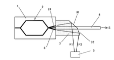
- FIG. 1 shows a first embodiment of the optical modulator of the present invention.
- the present invention includes a substrate 1 having an electro-optic effect, an optical waveguide 2 including Mach-Zehnder optical waveguides (21 to 24) formed on the substrate, and a modulation electrode for modulating a light wave propagating through the optical waveguide (Not shown) and an optical modulator having an optical fiber 4 for guiding light emitted from the optical waveguide, two radiated lights (R1, R2) emitted from the Mach-Zehnder optical waveguide are Condensing means (31, 32) which condenses toward the light receiving element 5, and a light quantity ratio adjusting means for adjusting a light quantity ratio of the two radiated lights received by the light receiving element 5.
- reflecting means (31, 32) provided in the reinforcing capillary 3 for connecting the optical fiber 4 to the end of the substrate 1 as shown in FIG. It is possible to use.
- the two radiated lights (R1, R2) generated in the combined portion 23 are received by one light receiving element 5 having a small light receiving diameter. It becomes possible to receive light. Thereby, the phase difference between the monitor light and the optical fiber output light S can be compensated, and good monitor characteristics can be obtained.
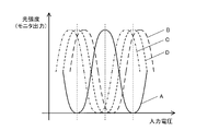
- the light intensity of the outgoing light S from the optical fiber is represented by a graph A in FIG.
- the horizontal axis of the graph represents the bias voltage (input voltage) applied to the modulation electrode.
- the light intensities of the two emitted lights (R1, R2) are denoted by B and C.
- B and C the intensity of the emitted lights
- the intensity of the emitted light changes in a phase opposite to that of the output light, and the electric field amplitudes of the two emitted lights are opposite to each other. If a part of light that is a conversion loss in On light (in-phase state with On light) is mixed with this, the light intensities of the two radiated lights (R1, R2) are displayed as B and C in FIG.
- a light amount ratio adjusting means for adjusting a light amount ratio of two radiated lights received by the light receiving element.
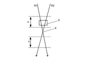
- the light quantity ratio adjusting means can be configured as means for adjusting the arrangement position of the light receiving elements. For example, as shown in FIG. 3, the propagation directions of the two radiated lights R1 and R2 are set to intersect with each other, and the light receiving surface of the light receiving element 5 is adjusted to be disposed within a predetermined range h while avoiding the intersection X. ing. This “intersection” is not limited to the case where the propagation direction of the radiated light is in the same plane.
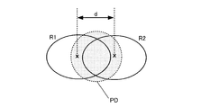
- the light receiving element 5 can be installed with its position adjusted in the vertical and horizontal directions in FIG. As a result, as shown in FIG. 4, the position of the light receiving surface PD can be changed relative to the beam shape of the radiated light R1 and the beam shape of the radiated light R2, and the radiated light R1 incident on the light receiving element can be changed. And the light intensity of R2 can be changed.
- the position of the light receiving element 5 is such that the optical path interval d (peak interval of the light intensity distribution) of the two radiated lights (R1, R2) is 0.5 to 2 times the light receiving diameter of the light receiving element (the diameter of the light receiving surface PD). It is preferable to arrange in the position. If it is less than 0.5 times, even if the light receiving element is moved in the left-right direction in FIG. 3 or FIG. It is difficult to efficiently receive both radiated light simultaneously with one light receiving element.
- the light receiving surface is not limited to a circular shape and may be a rectangular shape.
- the “light receiving diameter” corresponds to the length in the direction corresponding to the arrow d with the light receiving surface PD of FIG.
- the range h is arranged at a position deviating from the intersection X where two radiated lights intersect.
- the reflecting means provided in the reinforcing capillary 3 may be a flat surface as shown in FIG. 1 or a curved surface. Further, by configuring the reflection means to totally reflect the emitted light, the emitted light can be efficiently directed toward the light receiving element.
- the means for total reflection is realized by setting the end face angle of the capillary so that the relationship between the optical axis of the radiated light and the reflection surface satisfies total reflection, or by forming a mirror on the capillary reflection surface using a metal film. it can.
- the radiated light waveguide 6 disposed so as to sandwich the output waveguide 24 is provided. It is preferable. In particular, when a thin plate having a substrate thickness of 20 ⁇ m or less is used, it is possible to efficiently separate it from output light by providing a radiation waveguide.
- the position and direction in which the radiated light (R 1, R 2) is emitted to the reinforcing capillary 3 can be adjusted.
- the means (31, 32) it becomes possible to easily guide the two emitted lights to the proper positions.
- the substrate and the optical fiber or the reinforcing capillary are joined at an angle satisfying Snell's law, and it is also possible to prevent the light wave from being regularly reflected on the joining surface and going backward. is there.
- the light receiving element is disposed before or after the propagation direction of the emitted light intersects as shown in FIG. Therefore, an optical modulator having an optimum phase difference can be obtained even when there is a manufacturing error.
- the optical modulator and the optical fiber are optically connected by a spatial optical system using a condenser lens without using a reinforcing capillary as in Patent Document 4.
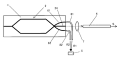
- a radiated light waveguide (61, 62) that guides the radiated light is formed on the substrate 1. It can also be used. This can be realized by adjusting the shape of the radiated light waveguide so that the radiated light (R1, R2) emitted from the radiated light waveguide (61, 62) is directed toward the light receiving element 5.
- Reference numeral 7 in FIG. 7 is a condensing lens for guiding output light (emitted light) S from the optical modulator to the optical fiber 4.
- optical fibers (81, 82) for guiding the radiated light as shown in FIG. 8 and to guide the radiated light (R 1, R 2) to the light receiving element 5. It is also possible to use a lens or a mirror instead of the optical fibers (81, 82).
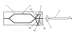
- the radiated light waveguide 62 is bent at the side surface of the substrate, and the reflecting means 63 such as a reflection film is disposed on the side surface, so that the two radiated lights (R1, R2) intersect on the substrate 1. It is also possible to configure as described above.
- the light receiving element 5 can receive two radiated lights propagating through the waveguide by being placed in contact with or close to the radiated light waveguide of the substrate 1. Naturally, by adjusting the position of the light receiving element 5 with respect to the waveguide for radiated light, the light quantity ratio of the two radiated lights received by the light receiving element can be adjusted.
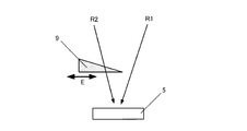
- the light modulator of the present invention it is also possible to use a light intensity adjusting filter 9 as shown in FIG. 10 instead of the light receiving element position adjusting means described above as the light quantity ratio adjusting means.
- the light intensity adjustment filter 9 is inserted in the optical path of at least one of the radiated lights, and the light quantity ratio between the two radiated lights incident on the light receiving element 5 is adjusted.
- the filter 9 By configuring the filter 9 so that the light transmittance changes depending on the amount of insertion, the amount of light can be adjusted at various levels.
- the optical modulator can compensate for the phase difference between the output light of the optical modulator and the monitor light and can be downsized with a simple configuration. Can be provided.
Landscapes
- Physics & Mathematics (AREA)
- Nonlinear Science (AREA)
- General Physics & Mathematics (AREA)
- Optics & Photonics (AREA)
- Chemical & Material Sciences (AREA)
- Engineering & Computer Science (AREA)
- Ceramic Engineering (AREA)
- Crystallography & Structural Chemistry (AREA)
- Optical Modulation, Optical Deflection, Nonlinear Optics, Optical Demodulation, Optical Logic Elements (AREA)
Abstract
La présente invention a pour objet un modulateur de lumière qui peut compenser une différence de phase entre la lumière de sortie du modulateur de lumière et une lumière d'un moniteur, a une structure simple et peut être miniaturisé. Un modulateur de lumière comprend : un substrat (1) ayant un effet électro-optique ; un guide d'ondes optiques (2) qui contient des guides d'ondes optiques de type Mach-Zehnder (21 à 24) formés sur le substrat ; une électrode de modulation permettant de moduler les ondes de lumière propagées à travers le guide d'ondes optiques ; et une fibre optique (4) qui guide la lumière projetée par le guide d'ondes optiques. Le modulateur de lumière est caractérisé en ce qu'il comprend les moyens suivants : un moyen de concentration de lumière (31, 32) qui concentre deux rayons lumineux propagés (R1, R2) émis par les guides d'ondes optiques de type Mach-Zehnder vers un unique élément de réception de lumière (5) ; et un moyen d'ajustement du rapport d'intensité de la lumière qui ajuste le rapport d'intensité de la lumière des deux rayons lumineux propagés reçus par l'élément de réception de lumière (5).
Priority Applications (3)
| Application Number | Priority Date | Filing Date | Title |
|---|---|---|---|
| CN201280010366.6A CN103392146B (zh) | 2011-02-23 | 2012-02-22 | 光调制器 |
| US14/001,059 US8923673B2 (en) | 2011-02-23 | 2012-02-22 | Optical modulator |
| EP12749790.7A EP2680061B1 (fr) | 2011-02-23 | 2012-02-22 | Modulateur de lumière |
Applications Claiming Priority (4)
| Application Number | Priority Date | Filing Date | Title |
|---|---|---|---|
| JP2011-037719 | 2011-02-23 | ||
| JP2011037719A JP4977789B1 (ja) | 2011-02-23 | 2011-02-23 | 光変調器 |
| JP2011-037718 | 2011-02-23 | ||
| JP2011037718A JP4977788B1 (ja) | 2011-02-23 | 2011-02-23 | 光変調器 |
Publications (1)
| Publication Number | Publication Date |
|---|---|
| WO2012115133A1 true WO2012115133A1 (fr) | 2012-08-30 |
Family
ID=46720909
Family Applications (1)
| Application Number | Title | Priority Date | Filing Date |
|---|---|---|---|
| PCT/JP2012/054228 Ceased WO2012115133A1 (fr) | 2011-02-23 | 2012-02-22 | Modulateur de lumière |
Country Status (4)
| Country | Link |
|---|---|
| US (1) | US8923673B2 (fr) |
| EP (1) | EP2680061B1 (fr) |
| CN (1) | CN103392146B (fr) |
| WO (1) | WO2012115133A1 (fr) |
Cited By (2)
| Publication number | Priority date | Publication date | Assignee | Title |
|---|---|---|---|---|
| US20150261060A1 (en) * | 2012-08-31 | 2015-09-17 | Sumitomo Osaka Cement Co., Ltd. | Light modulator |
| US20170012700A1 (en) * | 2014-01-31 | 2017-01-12 | Sumitomo Osaka Cement Co., Ltd. | Optical device |
Families Citing this family (6)
| Publication number | Priority date | Publication date | Assignee | Title |
|---|---|---|---|---|
| JP2013122546A (ja) * | 2011-12-12 | 2013-06-20 | Sumitomo Electric Ind Ltd | 半導体光位相変調器及びその駆動方法 |
| JP6056800B2 (ja) * | 2014-03-31 | 2017-01-11 | 住友大阪セメント株式会社 | 光変調器 |
| US10423008B2 (en) * | 2015-01-14 | 2019-09-24 | 3M Innovative Properties Company | Eyewear lens attachment assembly |
| US9715066B2 (en) * | 2015-12-24 | 2017-07-25 | Intel Corporation | Double-sided orthogonal grating optical coupler |
| JP2021509483A (ja) * | 2017-12-26 | 2021-03-25 | 住友電気工業株式会社 | 光モジュール及び光モジュールの組立方法 |
| JP7585940B2 (ja) * | 2021-03-31 | 2024-11-19 | 住友大阪セメント株式会社 | 光導波路素子とそれを用いた光変調デバイス並びに光送信装置 |
Citations (8)
| Publication number | Priority date | Publication date | Assignee | Title |
|---|---|---|---|---|
| JPH0553086A (ja) * | 1991-08-28 | 1993-03-05 | Fujitsu Ltd | マツハツエンダー型光導波路デバイス |
| JPH0566334A (ja) * | 1991-09-10 | 1993-03-19 | Fujitsu Ltd | 受光器モジユール |
| JPH1144867A (ja) | 1997-07-25 | 1999-02-16 | Fujitsu Ltd | 光変調器モジュール |
| JP2001281507A (ja) | 2000-03-31 | 2001-10-10 | Sumitomo Osaka Cement Co Ltd | 出力光モニタ付光導波路型光変調器 |
| US6795620B2 (en) | 2002-11-27 | 2004-09-21 | Codeon Corporation | Fiber tail assembly with optical signal tap |
| WO2005124438A1 (fr) * | 2004-06-15 | 2005-12-29 | Anritsu Corporation | Modulateur optique avec photodétecteur à moniteur |
| JP2006301612A (ja) * | 2005-03-25 | 2006-11-02 | Sumitomo Osaka Cement Co Ltd | 光変調器 |
| JP2010237376A (ja) | 2009-03-31 | 2010-10-21 | Sumitomo Osaka Cement Co Ltd | 光変調器 |
Family Cites Families (13)
| Publication number | Priority date | Publication date | Assignee | Title |
|---|---|---|---|---|
| FR2546309B1 (fr) * | 1983-05-19 | 1986-07-04 | Yi Yan Alfredo | Structure de guidage optique utilisant un reseau de diffraction |
| US4846540A (en) * | 1988-01-25 | 1989-07-11 | Bell Communications Research, Inc. | Optical wavegide junction |
| US5627929A (en) * | 1995-05-04 | 1997-05-06 | Sandia Corporation | Integrated optical XY coupler |
| US6240118B1 (en) * | 1998-11-16 | 2001-05-29 | Lucent Technologies Inc. | Multichannel laser transmitter with a single output port |
| US7200289B2 (en) * | 2000-03-15 | 2007-04-03 | Sumitomo Osaka Cement Co., Ltd. | Optical waveguide modulator with output light monitor |
| EP1818712B1 (fr) | 2000-03-15 | 2012-09-26 | Sumitomo Osaka Cement Co., Ltd. | Modulateur à guide d'onde optique avec moniteur lumineux de sortie |
| JP3974792B2 (ja) * | 2002-02-07 | 2007-09-12 | 富士通株式会社 | 光導波路デバイス及び光デバイス |
| JP4911529B2 (ja) * | 2005-02-22 | 2012-04-04 | 日本碍子株式会社 | 光変調器 |
| US7444039B2 (en) | 2005-03-25 | 2008-10-28 | Sumitomo Osaka Cement Co., Ltd. | Optical modulator |
| JP4879637B2 (ja) * | 2006-04-20 | 2012-02-22 | 住友大阪セメント株式会社 | 光変調装置 |
| US7783138B2 (en) * | 2007-11-16 | 2010-08-24 | Jds Uniphase Corporation | Free-space integrated photodetector with reduced phase tracking error |
| JP5012624B2 (ja) * | 2008-03-31 | 2012-08-29 | 住友大阪セメント株式会社 | 光導波路素子 |
| US8849071B2 (en) * | 2009-12-30 | 2014-09-30 | Jds Uniphase Corporation | Optical waveguide modulator |
-
2012
- 2012-02-22 WO PCT/JP2012/054228 patent/WO2012115133A1/fr not_active Ceased
- 2012-02-22 CN CN201280010366.6A patent/CN103392146B/zh not_active Expired - Fee Related
- 2012-02-22 US US14/001,059 patent/US8923673B2/en active Active
- 2012-02-22 EP EP12749790.7A patent/EP2680061B1/fr not_active Not-in-force
Patent Citations (8)
| Publication number | Priority date | Publication date | Assignee | Title |
|---|---|---|---|---|
| JPH0553086A (ja) * | 1991-08-28 | 1993-03-05 | Fujitsu Ltd | マツハツエンダー型光導波路デバイス |
| JPH0566334A (ja) * | 1991-09-10 | 1993-03-19 | Fujitsu Ltd | 受光器モジユール |
| JPH1144867A (ja) | 1997-07-25 | 1999-02-16 | Fujitsu Ltd | 光変調器モジュール |
| JP2001281507A (ja) | 2000-03-31 | 2001-10-10 | Sumitomo Osaka Cement Co Ltd | 出力光モニタ付光導波路型光変調器 |
| US6795620B2 (en) | 2002-11-27 | 2004-09-21 | Codeon Corporation | Fiber tail assembly with optical signal tap |
| WO2005124438A1 (fr) * | 2004-06-15 | 2005-12-29 | Anritsu Corporation | Modulateur optique avec photodétecteur à moniteur |
| JP2006301612A (ja) * | 2005-03-25 | 2006-11-02 | Sumitomo Osaka Cement Co Ltd | 光変調器 |
| JP2010237376A (ja) | 2009-03-31 | 2010-10-21 | Sumitomo Osaka Cement Co Ltd | 光変調器 |
Non-Patent Citations (1)
| Title |
|---|
| See also references of EP2680061A4 |
Cited By (3)
| Publication number | Priority date | Publication date | Assignee | Title |
|---|---|---|---|---|
| US20150261060A1 (en) * | 2012-08-31 | 2015-09-17 | Sumitomo Osaka Cement Co., Ltd. | Light modulator |
| US9377666B2 (en) * | 2012-08-31 | 2016-06-28 | Sumitomo Osaka Cement Co., Ltd. | Light modulator |
| US20170012700A1 (en) * | 2014-01-31 | 2017-01-12 | Sumitomo Osaka Cement Co., Ltd. | Optical device |
Also Published As
| Publication number | Publication date |
|---|---|
| CN103392146A (zh) | 2013-11-13 |
| EP2680061A4 (fr) | 2014-07-09 |
| EP2680061A1 (fr) | 2014-01-01 |
| US20140023310A1 (en) | 2014-01-23 |
| EP2680061B1 (fr) | 2016-06-22 |
| CN103392146B (zh) | 2015-05-06 |
| US8923673B2 (en) | 2014-12-30 |
Similar Documents
| Publication | Publication Date | Title |
|---|---|---|
| JP5782974B2 (ja) | 光変調器及び光変調器の受光素子の受光量調整方法 | |
| CN103392146B (zh) | 光调制器 | |
| JP5621861B2 (ja) | 光デバイス | |
| JP5070853B2 (ja) | 光デバイス | |
| US20060133713A1 (en) | Optical waveguide modulator equipped with an output light monitor | |
| US7783138B2 (en) | Free-space integrated photodetector with reduced phase tracking error | |
| US9703169B2 (en) | Optical modulator | |
| CN103261961A (zh) | 用于监控调制器的输出特性的组件 | |
| CN108693603B (zh) | 光学元件模块 | |
| JP4977789B1 (ja) | 光変調器 | |
| US6795620B2 (en) | Fiber tail assembly with optical signal tap | |
| JP2015138145A (ja) | 光変調器 | |
| JP4977788B1 (ja) | 光変調器 | |
| JP2012203334A (ja) | 光学素子 | |
| JP6561248B1 (ja) | 集積型光デバイス | |
| US10551714B2 (en) | Optical device | |
| CN103492920B (zh) | 光学部件 | |
| US7474812B2 (en) | Monitor photodetector equipped optical modulator | |
| CN110927872A (zh) | 具有大光程差的光波导强度调制器芯片 | |
| JP2012211971A (ja) | 偏波合成装置 | |
| JPH0674792A (ja) | 光学式エンコーダ | |
| CN119374572A (zh) | 一种基于硅基薄膜铌酸锂的光纤陀螺引擎 | |
| JP2005352469A (ja) | 可変光減衰器 | |
| JP2019028367A (ja) | 光学素子及びその製造方法 | |
| JP2006242840A (ja) | 光電界センサおよび光電界センサの指向性調整方法 |
Legal Events
| Date | Code | Title | Description |
|---|---|---|---|
| 121 | Ep: the epo has been informed by wipo that ep was designated in this application |
Ref document number: 12749790 Country of ref document: EP Kind code of ref document: A1 |
|
| NENP | Non-entry into the national phase |
Ref country code: DE |
|
| WWE | Wipo information: entry into national phase |
Ref document number: 2012749790 Country of ref document: EP |
|
| WWE | Wipo information: entry into national phase |
Ref document number: 14001059 Country of ref document: US |