WO2012115267A1 - Elément de conversion photoélectrique et dispositif de conversion photoélectrique - Google Patents
Elément de conversion photoélectrique et dispositif de conversion photoélectrique Download PDFInfo
- Publication number
- WO2012115267A1 WO2012115267A1 PCT/JP2012/054771 JP2012054771W WO2012115267A1 WO 2012115267 A1 WO2012115267 A1 WO 2012115267A1 JP 2012054771 W JP2012054771 W JP 2012054771W WO 2012115267 A1 WO2012115267 A1 WO 2012115267A1
- Authority
- WO
- WIPO (PCT)
- Prior art keywords
- layer
- photoelectric conversion
- semiconductor layer
- light absorption
- group
- Prior art date
- Legal status (The legal status is an assumption and is not a legal conclusion. Google has not performed a legal analysis and makes no representation as to the accuracy of the status listed.)
- Ceased
Links
Images








Classifications
-
- H—ELECTRICITY
- H10—SEMICONDUCTOR DEVICES; ELECTRIC SOLID-STATE DEVICES NOT OTHERWISE PROVIDED FOR
- H10F—INORGANIC SEMICONDUCTOR DEVICES SENSITIVE TO INFRARED RADIATION, LIGHT, ELECTROMAGNETIC RADIATION OF SHORTER WAVELENGTH OR CORPUSCULAR RADIATION
- H10F77/00—Constructional details of devices covered by this subclass
- H10F77/20—Electrodes
- H10F77/244—Electrodes made of transparent conductive layers, e.g. transparent conductive oxide [TCO] layers
- H10F77/247—Electrodes made of transparent conductive layers, e.g. transparent conductive oxide [TCO] layers comprising indium tin oxide [ITO]
-
- H—ELECTRICITY
- H10—SEMICONDUCTOR DEVICES; ELECTRIC SOLID-STATE DEVICES NOT OTHERWISE PROVIDED FOR
- H10F—INORGANIC SEMICONDUCTOR DEVICES SENSITIVE TO INFRARED RADIATION, LIGHT, ELECTROMAGNETIC RADIATION OF SHORTER WAVELENGTH OR CORPUSCULAR RADIATION
- H10F10/00—Individual photovoltaic cells, e.g. solar cells
- H10F10/10—Individual photovoltaic cells, e.g. solar cells having potential barriers
- H10F10/16—Photovoltaic cells having only PN heterojunction potential barriers
- H10F10/167—Photovoltaic cells having only PN heterojunction potential barriers comprising Group I-III-VI materials, e.g. CdS/CuInSe2 [CIS] heterojunction photovoltaic cells
-
- H—ELECTRICITY
- H10—SEMICONDUCTOR DEVICES; ELECTRIC SOLID-STATE DEVICES NOT OTHERWISE PROVIDED FOR
- H10F—INORGANIC SEMICONDUCTOR DEVICES SENSITIVE TO INFRARED RADIATION, LIGHT, ELECTROMAGNETIC RADIATION OF SHORTER WAVELENGTH OR CORPUSCULAR RADIATION
- H10F77/00—Constructional details of devices covered by this subclass
- H10F77/10—Semiconductor bodies
- H10F77/14—Shape of semiconductor bodies; Shapes, relative sizes or dispositions of semiconductor regions within semiconductor bodies
- H10F77/147—Shapes of bodies
-
- Y—GENERAL TAGGING OF NEW TECHNOLOGICAL DEVELOPMENTS; GENERAL TAGGING OF CROSS-SECTIONAL TECHNOLOGIES SPANNING OVER SEVERAL SECTIONS OF THE IPC; TECHNICAL SUBJECTS COVERED BY FORMER USPC CROSS-REFERENCE ART COLLECTIONS [XRACs] AND DIGESTS
- Y02—TECHNOLOGIES OR APPLICATIONS FOR MITIGATION OR ADAPTATION AGAINST CLIMATE CHANGE
- Y02E—REDUCTION OF GREENHOUSE GAS [GHG] EMISSIONS, RELATED TO ENERGY GENERATION, TRANSMISSION OR DISTRIBUTION
- Y02E10/00—Energy generation through renewable energy sources
- Y02E10/50—Photovoltaic [PV] energy
- Y02E10/541—CuInSe2 material PV cells
Definitions
- the present invention relates to a photoelectric conversion element and a photoelectric conversion device.
- a photoelectric conversion device used for solar power generation or the like there is one in which a light absorption layer is formed of a chalcopyrite-based I-III-VI group compound semiconductor such as CIGS having a high light absorption coefficient.
- CIGS has a high light absorption coefficient and is suitable for reducing the thickness, area, and cost of photoelectric conversion devices, and research and development of next-generation solar cells using the photoelectric conversion device is being promoted.
- the photoelectric conversion element includes a lower electrode such as a metal electrode on a substrate such as glass, a photoelectric conversion layer that is a semiconductor layer including a light absorption layer and a buffer layer, and an upper electrode such as a transparent electrode and a metal electrode. These are stacked in this order.
- the plurality of photoelectric conversion elements are electrically connected in series by electrically connecting the upper electrode of one adjacent photoelectric conversion element and the lower electrode of the other photoelectric conversion element by a connecting conductor. ing.
- CdS is deposited on a light absorption layer by a chemical deposition method to a thickness of 10 nm to form a buffer layer, and a binary target of a ZnO target and an MgO target is formed on the buffer layer.
- the upper electrode layer made of Zn 0.85 Mg 0.15 O and having a thickness of 1.2 ⁇ m is formed by the sputtering method used (see, for example, Patent Document 1).
- an object of the present invention is to increase the photoelectric conversion efficiency of the photoelectric conversion element and the photoelectric conversion device.
- a photoelectric conversion element includes a lower electrode layer, a light absorption layer including a photoelectrically convertible compound semiconductor provided on the lower electrode layer, and the light absorption layer.
- a photoelectric conversion element having a semiconductor layer provided on the semiconductor layer and an upper electrode layer having a lower resistivity than the semiconductor layer provided on the semiconductor layer, wherein the semiconductor layer is disposed on the upper electrode layer side.
- a porous layer region having a large number of pores.
- a photoelectric conversion element includes a lower electrode layer, a light absorption layer including a compound semiconductor capable of photoelectric conversion provided on the lower electrode layer, and the light absorption layer.
- a first semiconductor layer provided on the first semiconductor layer; a second semiconductor layer provided on the first semiconductor layer; and an upper electrode provided on the second semiconductor layer and having a lower resistivity than the second semiconductor layer.
- the first semiconductor layer has a first porous layer region having a large number of pores on the second semiconductor layer side.
- a photoelectric conversion device uses the photoelectric conversion element.
- the photoelectric conversion element and the photoelectric conversion device of the present invention it is possible to reduce damage caused by the sputtered particles being implanted into the light absorption layer or the like and to increase the photoelectric conversion efficiency.
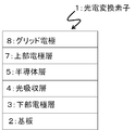
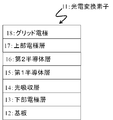
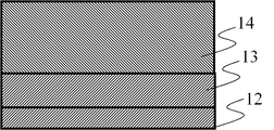
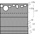
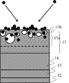
- FIG. 1 is a schematic diagram of a photoelectric conversion element according to a first embodiment. It is a cross-sectional schematic diagram of the manufacturing process of the photoelectric conversion element which concerns on 1st Embodiment. It is a cross-sectional schematic diagram of the manufacturing process of the photoelectric conversion element which concerns on 1st Embodiment. It is a cross-sectional schematic diagram of the manufacturing process of the photoelectric conversion element which concerns on 1st Embodiment. It is a cross-sectional schematic diagram of the manufacturing process of the photoelectric conversion element which concerns on 1st Embodiment.
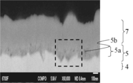
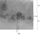
- FIG. 9 is an enlarged photograph substitution diagram within a dotted line in FIG. 8.
- It is a schematic diagram of the photoelectric conversion element which concerns on 2nd Embodiment.
- It is a cross-sectional schematic diagram of the manufacturing process of the photoelectric conversion element which concerns on 2nd Embodiment.
- It is a cross-sectional schematic diagram of the manufacturing process of the photoelectric conversion element which concerns on 2nd Embodiment.
- It is a cross-sectional schematic diagram of the manufacturing process of the photoelectric conversion element which concerns on 2nd Embodiment.
- It is a cross-sectional schematic diagram of the manufacturing process of the photoelectric conversion element which concerns on 2nd Embodiment.
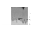
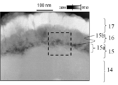
- FIG. 18 is an enlarged photograph substitute diagram within a dotted line in FIG. 17.
- the photoelectric conversion element 1 mainly includes a lower electrode layer 3, a light absorption layer 4, a semiconductor layer 5, an upper electrode layer 7, and a grid electrode 8 on a substrate 2.
- the material used for the substrate 2 examples include glass, ceramics, resin, and metal.
- a blue plate glass silica glass having a thickness of about 1 to 3 mm is used as the substrate 2.
- the lower electrode layer 3 is a conductor made of a metal such as Mo, Al, Ti, Ta or Au, or a laminated structure of these metals provided on one main surface of the substrate 2.
- the lower electrode layer 2 is formed to a thickness of about 0.2 to 1 ⁇ m using a known thin film forming method such as sputtering or vapor deposition.
- the light absorption layer 4 is a semiconductor layer having a p-type conductivity type and provided on the lower electrode layer 3 and containing, for example, a chalcopyrite-based (hereinafter also referred to as CIS-based) I-III-VI group compound. It is preferable.
- the light absorption layer 4 has a thickness of about 1 to 3 ⁇ m.
- the group I-III-VI compound is a group IB element, a group III-B element, and a group VI-B element (in other words, also referred to as a group 11, element, or group 16 element).
- Cu (In, Ga) Se 2 hereinafter also referred to as CIGS) and the like are exemplified, but the present invention is not limited thereto.
- Such a light absorbing layer 4 can be formed by a so-called vacuum process such as a sputtering method or a vapor deposition method, and a solution containing the constituent elements of the light absorbing layer 4 is applied on the lower electrode layer 3, and then It can also be formed by a so-called coating method or printing method in which drying and heat treatment are performed.
- the semiconductor layer 5 is a semiconductor layer provided on the light absorption layer 4 and having an n-type conductivity type different from the conductivity type of the light absorption layer 4.
- the semiconductor layer 5 is composed of a semiconductor layer having a compound semiconductor containing at least one of the II-B group element and the III-B group element provided on the light absorption layer 4, the semiconductor layer 5 is heterojunction with the light absorption layer 4. It is provided in the mode to do.
- the photoelectric conversion element 1 since photoelectric conversion occurs in the light absorption layer 4 and the semiconductor layer 5 constituting the heterojunction, the light absorption layer 4 and the semiconductor layer 5 are photoelectric conversion layers.
- the semiconductor layer 5 is preferably formed by a CBD method (chemical bath film formation method), for example, with a composition of In 2 S 3 system, ZnS system, CdS system, etc., and with a thickness of 1 to 30 nm. If possible, it may be formed by other means such as a thin film method or a plating method.
- CBD method chemical bath film formation method
- the upper electrode layer 7 is a transparent conductive film having an n-type conductivity provided on the semiconductor layer 5.
- the upper electrode layer 7 is provided as an electrode for extracting charges generated in the photoelectric conversion layer.
- the upper electrode layer 7 is made of a material having a resistivity lower than that of the semiconductor layer 5, such as indium oxide (ITO) containing tin, and the upper electrode layer 7 is formed by sputtering or vapor deposition. Formed by.
- ITO indium oxide
- the semiconductor layer 5 and the upper electrode layer 7 are preferably made of a material having light transmittance with respect to the wavelength region of the light absorbed by the light absorption layer 4, and the semiconductor layer 5 and the upper electrode layer 7. Are preferably substantially the same in absolute refractive index. Thereby, the fall of the light absorption efficiency to the light absorption layer 4 is suppressed.
- the grid electrode 8 including the current collector 8 a made of a metal such as Ag and the connecting portion 8 b takes out the electric charge generated in the photoelectric conversion element 1 from the upper electrode layer 7 and collects the current.
- the upper electrode layer 7 can be thinned.
- the grid electrode 8 preferably has a width of 50 to 400 ⁇ m in consideration of both conductivity and light transmittance to the light absorption layer 4.
- the semiconductor layer 5 will be described in detail.
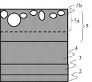
- the semiconductor layer 5 has a porous layer region having a large number of pores on the upper electrode layer 7 side.
- the light absorption layer 4, the semiconductor layer 5 provided on the light absorption layer 4, and the upper electrode layer 7 provided on the semiconductor layer 5 are provided.
- the semiconductor layer 5 has a porous layer region 5a having a large number of holes 5b on the upper electrode layer 7 side.
- the upper electrode layer 7 is formed by the sputtering method, pinning (striking) of the sputtered particles can be trapped and prevented by the holes 5b, and damage to the light absorption layer 4 can be reduced.
- the porous layer region 5a is a layer region in which a large number of holes 5b surrounded by the semiconductor layer 5 exist, that is, a large number of closed holes 5b are distributed on the upper electrode layer 7 side. It is preferable that pinned sputtered particles are easily captured.
- the pores 5b in the porous layer region 5a are, for example, portions that appear black in the TEM analysis photographs of FIGS.
- the semiconductor layer 5 contains sulfur element and oxygen element, and S / (S + O) absorbs light when the atomic% of the sulfur element contained in the semiconductor layer 5 is S and the atomic% of the oxygen element is O. It is preferable that the layer 4 side is larger.
- S / (S + O) is preferably 0.6 to 0.79.
- Each atomic% can be measured at each part of the semiconductor layer 5 by TEM EDS analysis, and it is preferable that this range be satisfied in the vicinity of the interface of the semiconductor layer 5 with the light absorption layer 4. .
- oxygen can be reduced and sulfur can be increased in the vicinity of the pn junction, so that the pn junction can be kept good.
- the light absorption layer includes a group IB element, a group III-B element, and a group VI-B element
- the semiconductor layer includes a group III-B element and a group VI-B element
- the porosity in the porous layer region 5a is preferably 10 to 80% in terms of area ratio.
- the sputtering particles are pinned (injected) by the holes 5b.
- damage to the light absorption layer 4 can be reduced.
- the porosity is obtained by binarizing the pore 5b in the porous region 5a and the portion without the pore 5b using an image processing analyzer, and measuring and calculating the respective areas. Can be sought.
- the photoelectric conversion efficiency can be increased.
- the lower electrode layer 13, the light absorption layer 14 including a compound semiconductor capable of photoelectric conversion provided on the lower electrode layer 13, and the light absorption layer 14 are provided.
- the first semiconductor layer 15 includes a first porous layer region 15a having a large number of pores 15b on the second semiconductor layer 16 side.
- the first semiconductor layer 51 has a first porous layer region 15a having a large number of holes 15b on the second semiconductor layer 16 side.
- the first porous layer region 15a is a layer region in which a large number of holes 15b surrounded by the first semiconductor layer 15 are present, that is, a large number of closed holes 5b are present on the second semiconductor layer 16 side. It is preferable that the pinned sputtered particles are easily captured.
- the first semiconductor layer 15 contains a sulfur element and an oxygen element
- S / is the atomic% of the sulfur element contained in the first semiconductor layer 15
- O is the atomic% of the oxygen element. It is preferable that (S + O) is configured to be larger toward the light absorption layer side.
- S / (S + O) is preferably 0.5 to 0.69.
- oxygen can be reduced and sulfur can be increased in the vicinity of the pn junction, so that the pn junction can be kept good.
- the light absorption layer 14 includes a group IB element, a group III-B element, and a group VI-B element
- the first semiconductor layer 15 includes a group III-B element and a group VI-B element
- the second semiconductor layer 16 may include a II-B group element and a VI-B group element.
- the first semiconductor layer 15 includes In 2 S 3 and the second semiconductor layer 16 includes ZnO.
- the porosity in the porous region 15a is preferably 10 to 80% in terms of area ratio.
- the porosity is obtained by binarizing the pore 15b in the porous region 15a and the portion without the pore 15b using an image processing analyzer, and measuring and calculating the respective areas. Can be sought.
- the second semiconductor layer 16 is formed by a sputtering method, pinning of the sputtered particles can be trapped and prevented by the holes 15b, and damage to the light absorption layer 14 can be further reduced.
- the thickness of the porous layer region 15a is 5 to 70 nm.
- a large number of electrons existing in the upper electrode layer 17 and the second semiconductor layer 16 are kept away from the holes of the p-type layer existing in the vicinity of the pn junction between the light absorption layer 14 and the first semiconductor layer 15 by the holes 15b. Can be easily done.
- the second semiconductor layer 16 is formed by the sputtering method, pinning (implantation) of the sputtered particles can be captured by the holes 15b, and damage to the light absorption layer 14 can be appropriately reduced.
- the present embodiment provides a photoelectric conversion device using a photoelectric conversion element.
- the photoelectric conversion device 10 includes a main surface on the side where the upper electrode layers 7 and 17 and the grid electrode 8 (8a is a current collecting portion and 8b is a connecting portion) are provided.
- the photoelectric conversion elements 1 and 11 are connected in series or in parallel to form a photoelectric conversion device 10.
- photoelectric conversion device 10 of the present invention is not limited to the above-described embodiment.
- a lower electrode layer 3 made of Mo is formed by sputtering on substantially the entire surface of the cleaned substrate 2, and light absorption made of an I-III-VI group compound semiconductor is formed on the lower electrode layer 3.
- the layer 4 (for example, CIGS including Cu, In, Ga, and Se) is formed using a coating method.
- a solution for forming the light absorption layer 4 is prepared by directly dissolving a group IB metal and a group III-B metal in a solvent containing a chalcogen element-containing compound and a basic organic solvent.
- the total concentration of the group B metal and the group III-B metal is 10% by mass or more.
- Various methods such as spin coater, screen printing, dipping, spraying, and die coater can be applied to the solution.
- the chalcogen element-containing organic compound is an organic compound containing a chalcogen element.
- chalcogen element S, Se, and Te among VI-B group elements are mentioned.
- the chalcogen element-containing organic compound include thiol, sulfide, selenol, tellurol and the like.
- To directly dissolve a metal in a mixed solvent means to dissolve a single metal or alloy ingot directly into the mixed solvent and dissolve it. Drying is desirably performed in a reducing atmosphere.
- the drying temperature is, for example, 50 to 300 ° C.
- the heat treatment is desirably performed in a reducing atmosphere such as a hydrogen atmosphere or a nitrogen atmosphere in order to prevent oxidation.
- the heat treatment temperature is 400 to 600 ° C., for example.
- the semiconductor layer 5 is formed by a CBD method (chemical bath film formation method) (see FIG. 4).
- the manufacturing method of the present embodiment includes a first step of forming a light absorption layer containing a group IB element, a group III-B element and a group VI-B element on the lower electrode layer,
- the circulation flow rate of the film-forming solution and the flow rate of the bubbling nitrogen are controlled so that the average particle size of the aggregates in the film-forming solution is 300 nm or more.
- the film forming temperature is controlled to be less than 500 nm, the film forming temperature of the film forming solution is in the range of 65 ° C. or higher and lower than 70 ° C., pH 2.4 or higher and lower than pH 2.6.
- the needle-like crystals are grown individually after the epitaxial growth, and the growth is performed.
- acicular crystals are grown and fused in the in-plane direction to grow a porous layer region 5a having a large number of holes 5b on the upper electrode layer 7 side (see FIG. 5).
- ph can be controlled by adding at least one of hydrochloric acid, acetic acid and nitric acid, or aqueous ammonia.
- the average particle size can be controlled by dividing the film-forming solution by centrifugal separation.
- ITO iridium oxide
- tin or the like is formed as the upper electrode layer 7 by a sputtering method or a vapor deposition method (see FIGS. 7, 8, and 9).
- the first semiconductor layer 15 is formed by a CBD method (chemical bath film formation method).
- the second semiconductor layer 16 is formed by a sputtering method in a later process, The thickness is preferably such that the absorption layer 14 can be protected from damage (see FIG. 12).
- the manufacturing method of the present embodiment includes a first step of forming a light absorption layer 14 containing a group IB element, a group III-B element, and a group VI-B element on the lower electrode layer 13, and a light
- a first semiconductor layer 15 containing a group III-B element and a group VI-B element is formed on the absorption layer 14 by the CBD method, and the atomic% C In and sulfur atoms of the film-forming solution in the CBD method
- It is preferable to have a second step of controlling so that% C S becomes C In : C S 1: 1 to 9 (preferably 2).
- the circulation flow rate of the film forming solution and the flow rate of the bubbling nitrogen are controlled, and the average particle size of the aggregates in the film forming solution is determined.
- the film-forming temperature of the film-forming solution is controlled to be in the range of from 65 to 70 ° C. and from pH 2.4 to less than 2.6.
- the needle-like crystals are grown individually after the epitaxial growth, and the growth is performed.
- acicular crystals are grown in the in-plane direction and fused to grow a first porous layer region 15a having a large number of holes 5b on the upper electrode layer 17 side (see FIG. 13).
- ph can be controlled by adding at least one of hydrochloric acid, acetic acid and nitric acid, or aqueous ammonia.
- the average particle size is achieved, and the particle size distribution can be managed by sizing the membrane solution by centrifugal separation.
- the sputtered particles pinned in the first porous layer region 15a can be captured (see FIGS. 14 and 15).
- ITO indium oxide containing ITO
- the upper electrode layer 17 is formed by a sputtering method or a vapor deposition method (see FIGS. 16, 17, and 18).
- Example 1 Photoelectric Conversion Element of First Embodiment (Sample Preparation)
- Example 1 relates to the case where the semiconductor layer has a single layer structure.
- a lower electrode layer 3 made of Mo is formed on substantially the entire surface of the cleaned glass substrate 2 by a sputtering method, and a light absorption layer 4 (CIGS containing Cu, In, Ga and Se) is applied on the lower electrode layer 3 Formed using.
- CIGS containing Cu, In, Ga and Se
- the concentration of the solution for forming the light absorption layer 4 was 10% by mass, applied with a spin coater, the drying temperature was 50 ° C. for 1 hour, and the heat treatment was performed in a nitrogen atmosphere at 400 ° C. for 1 hour.
- the semiconductor layer 5 was formed by the CBD method (chemical bath film formation method), and the upper electrode layer 7 was formed by the sputtering method in a later step.
- the circulation flow rate of the film-forming solution and the flow rate of the bubbling nitrogen are controlled so that the average particle size of the aggregates in the film-forming solution is 300 nm, and the film-forming solution is formed.
- the membrane temperature was controlled to 65 ° C. and pH 2.4.
- the needle-like crystals are grown during the growth process while growing the needle-like crystals individually after the epitaxial growth.
- the semiconductor layer 5 as a whole was grown to a thickness of 100 nm by growing in the in-plane direction and fusing. And the porous layer area
- ITO indium oxide
- the results are shown in Table 1 below.
- the porosity of the porous layer region 5a was controlled by the deposition rate of the porous layer region 5a, and the thickness of the porous layer region 5a was controlled by the deposition time of the porous layer region 5a.
- the semiconductor layer 5 is broken due to damage caused by pinning (striking) of the sputtered particles, and a defect is generated at the pn junction interface with the light absorption layer 4. Therefore, the photoelectric conversion efficiency was low.
- Samples 2 to 6, particularly Samples 3 to 5, showed good photoelectric conversion efficiency.
- Samples 7 to 11, particularly Samples 8 to 10 showed good photoelectric conversion efficiency, and showed a preferable range when the thickness of the porous layer region 5a was 5 to 70 nm.
- Example 2 Photoelectric Conversion Element of Second Embodiment (Sample Preparation)
- Example 2 relates to a case where the semiconductor layer has a two-layer structure.
- the process is the same as in Example 1 until the light absorption layer 14 is formed.
- the circulation flow rate of the film formation solution and the flow rate of the bubbling nitrogen are controlled so that the average particle size of the aggregates in the film formation solution is 300 nm.
- the film formation temperature of the solution was controlled to 65 ° C. and pH 2.4.
- the needle-like crystals are grown during the growth process while growing the needle-like crystals individually after the epitaxial growth.
- the porous layer region 15a having a large number of pores 15b on the second semiconductor layer 16 side is grown in the in-plane direction and fused, and the semiconductor layer 5 as a whole has a thickness of 100 nm.
- i-ZnO high resistance zinc oxide
- ITO indium oxide
- the circulation flow rate of the film formation solution and the flow rate of the bubbling nitrogen are controlled, and the average particle size of the aggregates in the film formation solution is 300 nm.
- the film-forming temperature of the film-forming solution is controlled to be 65 ° C. and pH 2.4
- the film formation is stopped before the acicular crystals are generated, and high resistance zinc oxide (i -ZnO) was prepared by forming indium oxide (ITO) as the upper electrode layer 7 by the sputtering method, so that the sample 12 having no porous layer region 15a was obtained.
- the results are shown in Table 2 below.
- the porosity of the first porous layer region 15a is the film formation speed of the first porous layer region 15a
- the thickness of the first porous layer region 15a is the film formation time of the first porous layer region 15a. Respectively.
- the first semiconductor layer 15 is broken due to damage due to pinning (implantation) of the sputtered particles, and the pn junction interface with the light absorption layer 14 is formed. Since a defect occurred, the photoelectric conversion efficiency was low.
- Samples 13 to 17, particularly Samples 14 to 16, showed good photoelectric conversion efficiency.
- Samples 18-22 showed good photoelectric conversion efficiency, and the thickness of the porous layer region 5a was found to be in a suitable range when it was 5-70 nm.
Landscapes
- Photovoltaic Devices (AREA)
- Recrystallisation Techniques (AREA)
Abstract
Lorsque de nombreux électrons présents dans une électrode transparente se trouvent à proximité de trous dans une couche absorbant la lumière, le nombre de défectuosités à l'interface de la jonction PN peut augmenter avec le temps. La solution proposée dans le cadre de cette invention consiste à utiliser un élément de conversion photoélectrique comprenant : une couche électrode inférieure; une couche d'absorption de la lumière disposée sur la couche électrode inférieure et comprenant un semi-conducteur composite capable de conversion photoélectrique; une couche semi-conductrice qui est disposée sur la couche d'absorption de la lumière; et une couche électrode supérieure qui est disposée sur la couche semi-conductrice et dont la résistivité électrique est inférieure à celle de cette couche semi-conductrice. La couche semi-conductrice présente une structure comportant une région de couche poreuse présentant de nombreux pores sur le côté couche électrode supérieure.
Priority Applications (1)
| Application Number | Priority Date | Filing Date | Title |
|---|---|---|---|
| JP2013501161A JPWO2012115267A1 (ja) | 2011-02-25 | 2012-02-27 | 光電変換素子および光電変換装置 |
Applications Claiming Priority (4)
| Application Number | Priority Date | Filing Date | Title |
|---|---|---|---|
| JP2011-040261 | 2011-02-25 | ||
| JP2011040261 | 2011-02-25 | ||
| JP2011164178 | 2011-07-27 | ||
| JP2011-164178 | 2011-07-27 |
Publications (1)
| Publication Number | Publication Date |
|---|---|
| WO2012115267A1 true WO2012115267A1 (fr) | 2012-08-30 |
Family
ID=46721034
Family Applications (1)
| Application Number | Title | Priority Date | Filing Date |
|---|---|---|---|
| PCT/JP2012/054771 Ceased WO2012115267A1 (fr) | 2011-02-25 | 2012-02-27 | Elément de conversion photoélectrique et dispositif de conversion photoélectrique |
Country Status (2)
| Country | Link |
|---|---|
| JP (1) | JPWO2012115267A1 (fr) |
| WO (1) | WO2012115267A1 (fr) |
Cited By (1)
| Publication number | Priority date | Publication date | Assignee | Title |
|---|---|---|---|---|
| JP2013012703A (ja) * | 2011-05-30 | 2013-01-17 | Kyocera Corp | 化合物半導体膜の製造方法および製造装置 |
Citations (4)
| Publication number | Priority date | Publication date | Assignee | Title |
|---|---|---|---|---|
| JPS5730379A (en) * | 1980-07-31 | 1982-02-18 | Agency Of Ind Science & Technol | Thin film solar battery |
| JPH0541531A (ja) * | 1991-05-27 | 1993-02-19 | Fuji Electric Corp Res & Dev Ltd | CuInSe2 系薄膜太陽電池およびその製造方法 |
| JP2006525671A (ja) * | 2003-05-08 | 2006-11-09 | ソリブロ エイビー | 薄膜太陽電池 |
| JP2010287607A (ja) * | 2009-06-09 | 2010-12-24 | Hitachi Ltd | タンデム型薄膜太陽電池 |
-
2012
- 2012-02-27 JP JP2013501161A patent/JPWO2012115267A1/ja active Pending
- 2012-02-27 WO PCT/JP2012/054771 patent/WO2012115267A1/fr not_active Ceased
Patent Citations (4)
| Publication number | Priority date | Publication date | Assignee | Title |
|---|---|---|---|---|
| JPS5730379A (en) * | 1980-07-31 | 1982-02-18 | Agency Of Ind Science & Technol | Thin film solar battery |
| JPH0541531A (ja) * | 1991-05-27 | 1993-02-19 | Fuji Electric Corp Res & Dev Ltd | CuInSe2 系薄膜太陽電池およびその製造方法 |
| JP2006525671A (ja) * | 2003-05-08 | 2006-11-09 | ソリブロ エイビー | 薄膜太陽電池 |
| JP2010287607A (ja) * | 2009-06-09 | 2010-12-24 | Hitachi Ltd | タンデム型薄膜太陽電池 |
Cited By (1)
| Publication number | Priority date | Publication date | Assignee | Title |
|---|---|---|---|---|
| JP2013012703A (ja) * | 2011-05-30 | 2013-01-17 | Kyocera Corp | 化合物半導体膜の製造方法および製造装置 |
Also Published As
| Publication number | Publication date |
|---|---|
| JPWO2012115267A1 (ja) | 2014-07-07 |
Similar Documents
| Publication | Publication Date | Title |
|---|---|---|
| JP5928612B2 (ja) | 化合物半導体太陽電池 | |
| US20110018089A1 (en) | Stack structure and integrated structure of cis based solar cell | |
| CN1350335A (zh) | 太阳能电池 | |
| JP2004296749A (ja) | 両面受光太陽電池 | |
| JP5178904B1 (ja) | Czts系薄膜太陽電池及びその製造方法 | |
| JP2001044464A (ja) | Ib―IIIb―VIb2族化合物半導体層の形成方法、薄膜太陽電池の製造方法 | |
| KR20080009346A (ko) | 태양전지 버퍼층의 제조방법 | |
| CN102628161A (zh) | 用于制造半导体膜和光伏装置的方法 | |
| JPWO2011136249A1 (ja) | 光電変換素子および光電変換装置ならびに光電変換素子の製造方法 | |
| US20130029450A1 (en) | Method for manufacturing solar cell | |
| KR101300791B1 (ko) | 전자빔 조사를 이용한 몰리브덴 박막의 전도도 향상 방법 | |
| JP2011119478A (ja) | 化合物半導体太陽電池 | |
| JP5641850B2 (ja) | 光電変換素子およびその製造方法 | |
| JPWO2012115267A1 (ja) | 光電変換素子および光電変換装置 | |
| CN102447008A (zh) | 光伏器件及其制造方法 | |
| CN102473768A (zh) | 太阳能电池及其制造方法 | |
| JP2012151432A (ja) | 光電変換素子および光電変換装置ならびに光電変換素子の製造方法 | |
| WO2012115265A1 (fr) | Elément de conversion photoélectrique et dispositif de conversion photoélectrique | |
| US20180240918A1 (en) | Photovoltaic devices including a chalcogenide-containing photovoltaic light-absorber, and related methods of making | |
| CN102496645A (zh) | 一种铜铟镓硒薄膜太阳能电池及其制备方法 | |
| JP2012079727A (ja) | 光電変換素子およびその製造方法 | |
| JP6738078B2 (ja) | 太陽電池及びその製造方法 | |
| KR101924538B1 (ko) | 투명 전도성 산화물 후면전극을 가지는 칼코게나이드계 태양전지 및 그 제조방법 | |
| CN102446989B (zh) | 光伏器件及其制造方法 | |
| Arredondo et al. | Study of electrical and morphological properties of AgInSe 2 thin films grown by co-evaporation |
Legal Events
| Date | Code | Title | Description |
|---|---|---|---|
| 121 | Ep: the epo has been informed by wipo that ep was designated in this application |
Ref document number: 12748911 Country of ref document: EP Kind code of ref document: A1 |
|
| ENP | Entry into the national phase |
Ref document number: 2013501161 Country of ref document: JP Kind code of ref document: A |
|
| NENP | Non-entry into the national phase |
Ref country code: DE |
|
| 122 | Ep: pct application non-entry in european phase |
Ref document number: 12748911 Country of ref document: EP Kind code of ref document: A1 |