WO2012117642A1 - Dispositif de conversion de puissance électrique, système de conversion de puissance électrique, et inverseur moteur - Google Patents
Dispositif de conversion de puissance électrique, système de conversion de puissance électrique, et inverseur moteur Download PDFInfo
- Publication number
- WO2012117642A1 WO2012117642A1 PCT/JP2011/078920 JP2011078920W WO2012117642A1 WO 2012117642 A1 WO2012117642 A1 WO 2012117642A1 JP 2011078920 W JP2011078920 W JP 2011078920W WO 2012117642 A1 WO2012117642 A1 WO 2012117642A1
- Authority
- WO
- WIPO (PCT)
- Prior art keywords
- power
- conversion
- signal
- voltage
- value
- Prior art date
- Legal status (The legal status is an assumption and is not a legal conclusion. Google has not performed a legal analysis and makes no representation as to the accuracy of the status listed.)
- Ceased
Links
Images


Classifications
-
- H—ELECTRICITY
- H02—GENERATION; CONVERSION OR DISTRIBUTION OF ELECTRIC POWER
- H02P—CONTROL OR REGULATION OF ELECTRIC MOTORS, ELECTRIC GENERATORS OR DYNAMO-ELECTRIC CONVERTERS; CONTROLLING TRANSFORMERS, REACTORS OR CHOKE COILS
- H02P27/00—Arrangements or methods for the control of AC motors characterised by the kind of supply voltage
- H02P27/04—Arrangements or methods for the control of AC motors characterised by the kind of supply voltage using variable-frequency supply voltage, e.g. inverter or converter supply voltage
- H02P27/06—Arrangements or methods for the control of AC motors characterised by the kind of supply voltage using variable-frequency supply voltage, e.g. inverter or converter supply voltage using DC to AC converters or inverters
- H02P27/08—Arrangements or methods for the control of AC motors characterised by the kind of supply voltage using variable-frequency supply voltage, e.g. inverter or converter supply voltage using DC to AC converters or inverters with pulse width modulation
-
- H—ELECTRICITY
- H02—GENERATION; CONVERSION OR DISTRIBUTION OF ELECTRIC POWER
- H02M—APPARATUS FOR CONVERSION BETWEEN AC AND AC, BETWEEN AC AND DC, OR BETWEEN DC AND DC, AND FOR USE WITH MAINS OR SIMILAR POWER SUPPLY SYSTEMS; CONVERSION OF DC OR AC INPUT POWER INTO SURGE OUTPUT POWER; CONTROL OR REGULATION THEREOF
- H02M7/00—Conversion of AC power input into DC power output; Conversion of DC power input into AC power output
- H02M7/02—Conversion of AC power input into DC power output without possibility of reversal
- H02M7/04—Conversion of AC power input into DC power output without possibility of reversal by static converters
- H02M7/12—Conversion of AC power input into DC power output without possibility of reversal by static converters using discharge tubes with control electrode or semiconductor devices with control electrode
- H02M7/21—Conversion of AC power input into DC power output without possibility of reversal by static converters using discharge tubes with control electrode or semiconductor devices with control electrode using devices of a triode or transistor type requiring continuous application of a control signal
- H02M7/217—Conversion of AC power input into DC power output without possibility of reversal by static converters using discharge tubes with control electrode or semiconductor devices with control electrode using devices of a triode or transistor type requiring continuous application of a control signal using semiconductor devices only
- H02M7/219—Conversion of AC power input into DC power output without possibility of reversal by static converters using discharge tubes with control electrode or semiconductor devices with control electrode using devices of a triode or transistor type requiring continuous application of a control signal using semiconductor devices only in a bridge configuration
-
- H—ELECTRICITY
- H02—GENERATION; CONVERSION OR DISTRIBUTION OF ELECTRIC POWER
- H02P—CONTROL OR REGULATION OF ELECTRIC MOTORS, ELECTRIC GENERATORS OR DYNAMO-ELECTRIC CONVERTERS; CONTROLLING TRANSFORMERS, REACTORS OR CHOKE COILS
- H02P2201/00—Indexing scheme relating to controlling arrangements characterised by the converter used
- H02P2201/03—AC-DC converter stage controlled to provide a defined DC link voltage
-
- H—ELECTRICITY
- H02—GENERATION; CONVERSION OR DISTRIBUTION OF ELECTRIC POWER
- H02P—CONTROL OR REGULATION OF ELECTRIC MOTORS, ELECTRIC GENERATORS OR DYNAMO-ELECTRIC CONVERTERS; CONTROLLING TRANSFORMERS, REACTORS OR CHOKE COILS
- H02P2201/00—Indexing scheme relating to controlling arrangements characterised by the converter used
- H02P2201/07—DC-DC step-up or step-down converter inserted between the power supply and the inverter supplying the motor, e.g. to control voltage source fluctuations, to vary the motor speed
Definitions
- the present invention relates to a power conversion device that converts AC voltage into DC, and a power conversion system and a motor inverter having the same.
- the power conversion circuit of this device is configured by connecting switching elements such as IGBTs (Insulated Gate Bipolar Transistors), for example, by bridge connection, and connecting diodes in antiparallel to each switching element.
- This type of power conversion circuit not only simply converts AC voltage to DC, but also normally has a function to approximate the waveform of the input AC current to a sine wave, a function to bring the power factor close to 1, and a DC output voltage. It has a function of controlling to a target value (desired value).
- Japanese Patent Application Laid-Open No. H10-228561 discloses a method for estimating a DC output voltage based on an input AC voltage or AC current instead of detecting a DC output voltage.
- the power converter that controls the DC output voltage to the target value it is possible to obtain a DC output voltage having a value as close to the desired value as possible.
- the main purpose of the power converter is to approximate the waveform of the input AC current to a sine wave, or to bring the power factor close to 1, etc., what is the target value of the DC output voltage? It becomes a problem whether to set to.
- the main circuit itself is a boost type.
- the direct-current output voltage needs to be controlled to at least a peak value of the input alternating voltage.
- the target value of the DC output voltage if the target value of the DC output voltage is set too low, the DC output voltage tends to be lower than the peak value of the AC voltage due to fluctuations in the input AC voltage. As a result, the waveform near the peak value of the input alternating current is distorted and the harmonic current increases. On the other hand, if the target value of the DC output voltage is set too high, the switching loss in each switching element increases, leading to a reduction in power conversion efficiency.
- the target value of the DC output voltage so as not to distort the input current waveform
- (1) the peak value of the input AC voltage is detected, and a certain margin is added to this peak value.
- (2) the efficiency of power conversion is somewhat sacrificed, but a value that is considered sufficiently higher than fluctuations in the input AC voltage is used as the target value.
- a fixed method may be used.
- the target value of the DC output voltage is dynamically adjusted so that the input current waveform is not distorted and the efficiency of power conversion is sufficiently high in the entire operating region having a certain width. Is difficult to set. Further, when a method involving detection or estimation of the DC output voltage is employed, a mechanism or operation for detecting or estimating the DC output voltage is required, resulting in an increase in cost of the power converter.
- an object of the present invention is to provide a power conversion device, a power conversion system, and a motor inverter that make it easy to dynamically set a target value of a DC output voltage.
- a power conversion device includes a switching element that performs switching according to a drive pulse signal, and a conversion circuit that performs AC-DC conversion on an input AC voltage by the switching.
- An operation signal generation unit that generates an operation signal that determines an operation amount of the switching element; and a pulse signal generation that performs pulse width modulation using the operation signal as a signal wave and generates the drive pulse signal according to the operation signal.
- the operation signal generation unit detects a modulation degree in the pulse width modulation, and generates the operation signal based on the detected value of the modulation degree.
- the conversion circuit has a bridge-type conversion circuit formed by bridge-connecting a plurality of the switching elements, and the operation signal generation unit receives an input alternating current.
- the operation signal may be generated so as to approach a sine wave having a power factor of 1.
- the operation signal generation unit feeds back the detected value of the modulation degree so that the modulation degree approaches a preset target value, or the modulation degree is
- the operation signal may be generated so as to fall within a preset allowable range.
- the operation signal generation unit may generate the operation signal so that the modulation degree approaches 1. More specifically, the conversion circuit may be configured to perform DC-AC conversion of voltage in a direction opposite to the direction of performing AC-DC conversion.
- the power conversion system includes the power conversion device having the above-described configuration and a DC-DC conversion circuit that performs bidirectional DC-DC conversion step-up or step-down, and the power conversion device includes the power An operation for outputting, from the DC-DC conversion circuit side, a DC voltage obtained by sequentially performing the AC-DC conversion and the DC-DC conversion on the AC voltage input to the converter side; and the DC An operation for outputting, from the power converter side, an AC voltage obtained by sequentially performing the DC-DC conversion and the DC-AC conversion on the DC voltage input to the DC conversion circuit.
- a power distribution system may be connected to the power conversion device side, and a secondary battery may be connected to the DC-DC conversion circuit side.
- the power conversion system can be used as a power conditioner for a secondary battery.
- a motor inverter includes a power converter according to the above configuration, a DC-AC converter circuit that receives a DC voltage obtained by the AC-DC conversion, and performs DC-AC conversion on the DC voltage.
- the DC-AC conversion circuit is configured to output an AC voltage obtained by the DC-AC conversion as a voltage for driving the motor.
- the power converter according to the present invention is provided using a converter circuit in which a plurality of switching elements that perform a switching operation in response to a pulse signal obtained by pulse width modulation using a signal wave and a carrier wave are connected in a bridge shape.
- a power conversion device that converts alternating current power into direct current power, wherein the power conversion device performs correction so that the amplitude of a signal wave and the amplitude of a carrier wave when performing the pulse width modulation approach the same value, The conversion is performed.
- the signal wave is calculated so that the power factor becomes 1 or a value in the vicinity of 1 based on a waveform of a difference between a voltage waveform in phase with the AC power and a current waveform of the AC power.
- the power converter is configured to adjust the amplitude of the voltage waveform or the current waveform as the correction.
- the pulse signal is controlled such that the maximum value of the ON duty ratio corresponding to the switching operation formed within one cycle of the carrier wave is close to 100% by the correction. To do.
- the pulse signal has a maximum ON duty ratio corresponding to the switching operation formed in one cycle of the carrier wave except for a section required for protecting the switching element of the conversion circuit,
- the correction is controlled to a value close to 100%.
- the power conversion device of the present invention no mechanism or operation for detecting or estimating the DC output voltage is required, the input current waveform is not distorted, and power conversion is performed. It becomes easy to dynamically set the target value of the DC output voltage so that the efficiency is sufficiently high. Moreover, according to the power conversion system and motor inverter which concern on this invention, it becomes possible to enjoy the advantage of the said power converter device.
- Configuration diagram of bidirectional power conditioner according to third embodiment of the present invention Configuration diagram of bidirectional power conditioner according to fourth embodiment of the present invention
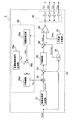
- FIG. 1 is a configuration diagram of the power conversion device 9. As shown in the figure, the power conversion device 9 includes a main circuit 1 and a control unit 2.
- the main circuit 1 includes a bridge type conversion circuit 11, a current / voltage detection circuit 12, a reactor L1, a capacitor C1, an output terminal T1, and the like.
- the main circuit 1 is connected to a single-phase AC power supply E1, and receives an AC input current Ii and an AC input voltage Vs from the single-phase AC power supply E1.
- the bridge type conversion circuit 11 has switching elements (Q1 to Q4) connected in a full bridge, and forms a PWM bridge type conversion circuit.
- the switching element is an NPN type IGBT, but other types such as a power MOSFET may be adopted.
- each switching element Q1 to Q4
- the collector of the switching element Q2 is connected to the emitter of the switching element Q1
- the collector of the switching element Q4 is connected to the emitter of the switching element Q3
- the collector of the switching element Q1 is connected.
- the collector of the switching element Q3 is connected, and the emitter of the switching element Q4 is connected to the emitter of the switching element Q2.
- connection point between the switching element Q3 and the switching element Q4 is connected to the positive side of the single-phase AC power supply E1 via the reactor L1, and the connection point between the switching element Q1 and the switching element Q2 is the single-phase AC power supply. Connected to the negative electrode side of E1. Further, the upper output end of the bridge type conversion circuit 11 (the connection point between the switching element Q1 and the switching element Q3) is connected to one end of the capacitor C1 and the upper output terminal T1, and the lower side of the bridge type conversion circuit 11 is connected to the lower side. The output end (the connection point between the switching element Q2 and the switching element Q4) is connected to the other end of the capacitor C1 and the lower output terminal T1.
- each switching element (Q1 to Q4) receives a drive pulse signal (G1 to G4) corresponding to itself from the control unit 2, and is turned on / off according to the inputted drive pulse signal. Switching.
- the current / voltage detection circuit 12 detects the waveforms of the AC input current Ii and the AC input voltage Vs.
- the current-voltage detection circuit 12 is a signal (referred to as “input current signal”) representing the waveform of the detected AC input current Ii and a signal (referred to as “input voltage signal”) representing the waveform of the detected AC input voltage Vs. ) Is output to the control unit 2.
- the control unit 2 generates drive pulse signals (G1 to G4) based on the input current signal and the input voltage signal input from the main circuit 1 side, and outputs them to the switching elements (Q1 to Q4).
- FIG. 2 is a configuration diagram of the control unit 2.
- the control unit 2 includes a reference sine wave generation unit 21, a multiplier 22, a subtractor 23, a PI controller 24, a compensation signal generation unit 25, an adder 26, a triangular wave generation unit 27, and a PWM comparator 28. , A modulation degree control unit 29, a gate drive circuit 30, and the like.
- the reference sine wave generation unit 21 performs a zero-cross detection process (detection process of timing when the voltage value becomes zero) and the like for the input voltage signal input from the main circuit 1 side, and is a reference in phase with the AC input voltage Vs Generate and output a sine wave.
- the multiplier 22 performs a process of multiplying the reference sine wave output from the reference sine wave generation unit 21 by a modulation degree correction value C MV (details will be described later).
- a waveform signal obtained by the multiplication is output to the subtractor 23.
- the subtracter 23 performs processing for subtracting the waveform of the AC input current Ii from the waveform of the signal output from the multiplier 22 based on the input current signal input from the main circuit 1 side. A signal having a waveform obtained by the subtraction is output to the PI controller 24.
- the PI controller 24 calculates an output value so that the value of the signal output from the subtracter 23 approaches zero, and outputs a signal representing this output value to the adder 26. That is, the PI controller 24 executes PI control so that the deviation between the waveform of the signal output from the multiplier 22 and the waveform of the AC input current Ii is small. As a result, the AC input current Ii is controlled to approach a sine wave with a power factor of 1.
- the compensation signal generation unit 25 generates a compensation signal for compensating for the back electromotive voltage generated in the main circuit 1. Based on the input current signal input from the main circuit 1 side, the compensation signal generation unit 25 generates a signal having a value obtained by multiplying the AC input voltage Vs by a predetermined coefficient K as a compensation signal, and outputs the signal to the adder 26.
- the adder 26 as an operation signal generation unit performs processing for adding the value of the compensation signal to the value of the output signal of the PI controller 24. Thereby, feedforward (FF) control for compensating the back electromotive voltage is realized.
- the waveform signal obtained by the addition is output to the non-inverting input terminal of the PWM comparator 28 and the modulation degree control unit 29 as the operation signal mv that determines the operation amount of the bridge type conversion circuit 11.
- the triangular wave generator 27 generates a reference triangular wave TRI signal having a predetermined period and amplitude, and outputs the generated signal to the inverting input terminal of the PWM comparator 28.
- the PWM comparator 28 as a pulse signal generation unit compares the values of the signals input to the input terminals, and generates a signal (a pulse signal in which H level and L level appear alternately) according to the comparison result.
- the PWM comparator 28 executes pulse width modulation (PWM) of a carrier modulation method using the operation signal mv as a signal wave and the reference triangular wave TRI as a carrier wave.
- the modulation degree MV in the pulse width modulation is represented by a ratio between the amplitude of the operation signal mv (signal wave) and the amplitude of the reference triangular wave TRI (carrier wave).
- the pulse signal generated by the PWM comparator 28 is output to the gate drive circuit 30.
- the modulation degree control unit 29 corrects feedback control for bringing the modulation degree MV closer to the target value, specifically, the amplitude of the signal wave and the amplitude of the carrier wave when performing pulse width modulation approach the same value. And includes a modulation degree detection unit 29a, a target modulation degree signal generation unit 29b, a subtractor 29c, and a PI controller 29d.
- the waveform (signal wave) of the signal output from the adder 26 is based on the waveform of the difference between the voltage waveform in phase with the AC input voltage Vs (AC power) and the current waveform of the AC input current Ii of AC power. It is a waveform calculated so that the rate becomes 1 or a value in the vicinity of 1.
- the modulation degree control unit 29 corrects the amplitude of the signal wave and the amplitude of the carrier wave so as to approach the same value by adjusting the amplitude of the waveform of the signal wave.
- the modulation degree detection unit 29a detects the amplitude of the input operation signal and modulates the current modulation, which is the ratio of the detection result (operation signal amplitude) and the reference triangular wave TRI amplitude (predetermined value).
- the degree MV is detected.
- the amplitude of the reference triangular wave TRI is set to 1, the amplitude of the detected operation signal can be regarded as the modulation degree.
- the detected signal indicating the current modulation degree MV is output to the subtractor 29c.
- the target modulation degree signal generation unit 29b generates a signal representing the target value of the modulation degree MV and outputs it to the subtractor 29c.
- the degree of modulation MV is 1 for the reason described later, and therefore it is usually preferable to set this target value to 1.
- the target value is not limited to 1.
- the target value may be slightly smaller than 1 in order to prevent the modulation degree MV from exceeding 1 more reliably.
- the target value may be fixed at all times or may be updated by a predetermined means.
- the subtractor 29c performs a process of subtracting the current modulation degree MV from the target modulation degree based on signals input from the modulation degree detection unit 29a and the target modulation degree signal generation unit 29b. A signal having a value obtained by the subtraction is output to the PI controller 29d.
- the PI controller 29d calculates the modulation degree correction value C MV described above so that the value of the signal output from the subtractor 29c approaches zero, and outputs a signal representing the modulation degree correction value C MV to the multiplier 22. To do. That is, the PI controller 29d performs PI control so that the deviation between the target modulation degree and the current modulation degree MV is small.
- the modulation degree correction value CMV is multiplied by the reference sine wave output from the reference sine wave generation unit 21.
- the modulation degree MV is feedback-controlled so as to approach the target value.
- the gate drive circuit 30 generates drive pulse signals (G1 to G4) according to the pulse signal input from the PWM comparator 28, and outputs the drive pulse signals (G1 to Q4). Thereby, PWM control of each switching element (Q1 to Q4) is realized.
- this pulse signal the largest value of the ON duty ratio corresponding to the switching operation formed within one cycle of the carrier wave reference (triangular wave TRI) is controlled to a value close to 100% by correction by the modulation degree control unit 29. Yes.
- this pulse signal has a maximum ON duty ratio corresponding to the switching operation formed within one cycle of the carrier wave (triangular wave TRI) and protects the switching elements (Q1 to Q4) of the conversion circuit (main circuit 1). Except for the interval required for the above, the correction by the modulation degree control unit 29 is controlled to a value close to 100%.
- the power converter 9 is configured as described above, and by switching the switching elements (Q1 to Q4) in the bridge type converter circuit 11, the AC input voltage Vs input from the single-phase AC power supply E1 is converted to DC. The voltage is converted into a voltage and output from the output terminal T1 as a DC output voltage Vo.
- control unit 2 controls the switching elements (Q1 to Q4) so that the AC input current Ii approaches a sine wave having a power factor of 1 and the modulation degree MV approaches a target value of 1.
- An operation signal mv that determines an operation amount is generated.
- the control unit 2 performs pulse width modulation of a carrier modulation method using the operation signal mv as a signal wave and the reference triangular wave TRI as a carrier wave, and generates drive pulse signals (G1 to G4) corresponding to the operation signal mv.
- the switching elements (Q1 to Q4) are driven.
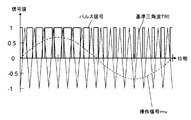
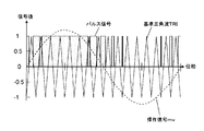
- FIG. 3 a schematic graph of a pulse signal or the like when the modulation degree MV is smaller than 1 (insufficient modulation) is shown in FIG. 3, and when the modulation degree MV is larger than 1 (overmodulation).
- 4 is a schematic graph of the pulse signal and the like generated in FIG.
- the degree of modulation MV is desirably maintained as close to 1 as possible.
- the modulation degree MV is dynamically controlled so as to always have a value near 1.
- the DC output voltage Vo is dynamically controlled so as to have an optimum value.
- the power converter 9 controls the modulation degree MV as described above, but the output voltage is not directly controlled. Therefore, when a power supply system to the load is formed using the power conversion device 9, a device for voltage adjustment (DC output) is provided between the power conversion device 9 and the load (that is, the rear stage side of the main circuit 1). A device that adjusts the voltage Vo so as to match the load may be provided. Thereby, while being able to supply an appropriate input voltage to the load, a power supply system utilizing the features of the power conversion device 9 is realized.
- FIG. 5 is a configuration diagram of the power conversion device 9a.
- the power conversion device 9 a includes a main circuit 3 and a control unit 4.
- the main circuit 3 includes a bridge type conversion circuit 31, a current / voltage detection circuit 32, a reactor (L1 to L3), a capacitor C1, and an output terminal T1.
- the main circuit 3 is connected to a three-phase AC power source E2, and from the three-phase AC power source E2, three-phase (U phase, V phase, and W phase) AC input currents (Iu, Iv, Iw) and an AC input voltage (Vu, Vv, Vw) is input.
- the subscripts u, v, and w represent the U phase, the V phase, and the W phase, respectively.
- the bridge type conversion circuit 31 has switching elements (Q1 to Q6) connected in a full bridge, and forms a PWM bridge type conversion circuit.
- the collector of the switching element Q2 is connected to the emitter of the switching element Q1
- the collector of the switching element Q4 is connected to the emitter of the switching element Q3, and the emitter of the switching element Q5 is connected.
- the collector of the switching element Q6 is connected.
- the collectors of switching elements Q1, Q3, and Q5 are connected to each other, and the emitters of switching elements Q2, Q4, and Q6 are connected to each other.
- connection point between the switching element Q1 and the switching element Q2 is connected to the U-phase power supply line of the three-phase AC power supply E2 via the reactor L1, and the connection point between the switching element Q3 and the switching element Q4 is connected to the reactor L2. Is connected to the V-phase power supply line of the three-phase AC power supply E2, and the connection point between the switching element Q5 and the switching element Q6 is connected to the W-phase power supply line of the three-phase AC power supply E2 via the reactor L3.
- the upper output terminal of the bridge type conversion circuit 31 (the connection point of the switching elements Q1, Q3, and Q5) is connected to one end of the capacitor C1 and the upper output terminal T1.
- the output end (the connection point of the switching elements Q2, Q4, and Q6) is connected to the other end of the capacitor C1 and the lower output terminal T1.
- Each switching element (Q1 to Q6) receives a drive pulse signal (G1 to G6) corresponding to the switching element (Q1 to Q6) from the control unit 4, and switches between conduction and non-conduction according to the drive pulse signal.
- the current voltage detection circuit 32 detects the waveform of the AC input current (Iu, Iv, Iw) and AC input voltage (Vu, Vv, Vw) of each phase.
- the current voltage detection circuit 12 outputs the detected waveform of the AC input current of each phase and the detected waveform of each AC input voltage to the control unit 4.
- the control unit 4 generates drive pulse signals (G1 to G6) based on the input current signal and the input voltage signal input from the main circuit 3 side, and outputs them to the switching elements (Q1 to Q6).
- FIG. 6 is a configuration diagram of the control unit 4.
- the control unit 4 includes a coordinate conversion unit 41 corresponding to the current value, a subtracter (42a, 42b), a PI controller (43a, 43b), a coordinate conversion unit 44 corresponding to the voltage value, and a compensation.
- a signal generation unit (45a, 45b), an adder (46a, 46b), an inverse coordinate conversion unit 47, a triangular wave generation unit 48, a PWM pulse generation unit 49, a modulation degree control unit 50, and a gate drive circuit 51 are provided. .
- the coordinate conversion unit 41 performs coordinate conversion (including three-phase two-phase conversion and rotational coordinate conversion) on the waveform of the AC input current of each phase input from the main circuit 3 side, and d-axis component (effective) of the AC input current Current component) signal Id and q-axis component (reactive current component) signal Iq.
- the signal Id is output to the subtractor 42a, and the signal Iq is output to the subtractor 42b.
- the subtractor 42a performs a process of subtracting the value of the signal Id from the modulation degree correction value C MV (described later in detail). A signal having a value obtained by the subtraction is output to the PI controller 43a.
- the subtractor 42b performs a process of subtracting the value of the signal Iq from the zero current value (0A). A signal having a value obtained by the subtraction is output to the PI controller 43b.
- the PI controller 43a calculates an output value so that the value of the signal output from the subtractor 42a approaches zero, and outputs a signal representing this output value to the adder 46a. That is, the PI controller 43a performs PI control so that the deviation between the modulation degree correction value CMV and the value of the signal Id becomes small. In this way, the amplitude of the effective current component is controlled.
- the PI controller 43b calculates an output value so that the value of the signal output from the subtractor 42b approaches zero, and outputs a signal representing this output value to the adder 46b. That is, the PI controller 43b executes PI control so that the value of the signal Iq approaches zero. In this way, the amplitude of the reactive current component is adjusted to approach zero so that the power factor 1 is maintained, and the AC input current is controlled to approach a sine wave having a power factor of 1.
- the coordinate conversion unit 44 performs coordinate conversion on the waveform of the AC input voltage of each phase input from the main circuit 3 side, and generates a d-axis component signal Vd and a q-axis component signal Vq of the AC input voltage.
- the signal Vd is output to the compensation signal generation unit 45a, and the signal Vq is output to the compensation signal generation unit 45b.
- the compensation signal generators (45a, 45b) generate a compensation signal for compensating the back electromotive voltage generated in the main circuit 3. More specifically, the compensation signal generation unit 45a generates a signal having a value obtained by multiplying the value of the signal Vd by a predetermined coefficient K1 as a compensation signal, and outputs the signal to the adder 46a. Further, the compensation signal generation unit 45b generates a signal having a value obtained by multiplying the value of the signal Vq by a predetermined coefficient K2 as a compensation signal, and outputs the signal to the adder 46b.
- the adder 46a performs a process of adding the value of the compensation signal output from the compensation signal generator 45a to the output value of the PI controller 43a.
- a signal having a value obtained by the addition is output to the inverse coordinate conversion unit 47 and the modulation degree control unit 50 as a signal (converter amplitude md) corresponding to the amplitude of the adjusted effective current component.
- the adder 46b performs a process of adding the value of the compensation signal output from the compensation signal generation unit 45b to the output value of the PI controller 43b.
- a signal having a value obtained by the addition is output to the inverse coordinate conversion unit 47 as a signal corresponding to the amplitude of the reactive current component after adjustment.
- the inverse coordinate conversion unit 47 performs inverse coordinate conversion (inverse of the coordinate conversion performed by the coordinate conversion unit 41) on the input signal (d-axis value) from the adder 46a and the input signal (q-axis value) from the adder 46b. Process).
- an operation signal mu corresponding to the U phase, an operation signal mv corresponding to the V phase, and an operation signal mw corresponding to the W phase are generated as operation signals for determining the operation amount of the bridge type conversion circuit 11.
- the These operation signals are output to the PWM pulse generator 49.
- the triangular wave generation unit 48 generates a reference triangular wave TRI signal having a predetermined period and amplitude, and outputs the signal to the PWM pulse generation unit 49.
- the PWM pulse generator 49 compares the values of the operation signal and the reference triangular wave TRI for each of the U phase, the V phase, and the W phase, and a signal (H level and L level alternately) according to the comparison result. Appearing pulse signal).
- the PWM pulse generator 49 performs pulse width modulation (PWM) of a carrier modulation method using the operation signal of each phase as a signal wave and the reference triangular wave TRI as a carrier wave.
- the modulation degree MD in the pulse width modulation is represented by a ratio between the amplitude of the operation signal (signal wave) and the amplitude of the reference triangular wave TRI (carrier wave).
- Each pulse signal generated by the PWM pulse generator 49 is output to the gate drive circuit 51.
- the modulation degree control unit 50 performs feedback control for bringing the modulation degree MD close to the target value.
- the modulation degree detection unit 50a performs scale conversion by dividing the value of the signal input from the adder 46a by the amplitude (predetermined value) of the reference triangular wave TRI. Since the value of the signal input from the adder 46a represents the amplitude of the operation signal, the current modulation degree MD is detected by the scale conversion. When the amplitude of the reference triangular wave TRI is set to 1, the value of the signal input from the adder 46a can be regarded as the modulation degree. The detected signal representing the current modulation degree MD is output to the subtractor 50c.
- the target modulation degree signal generation unit 50b generates a signal representing the target value of the modulation degree MD and outputs it to the subtracter 50c.
- the modulation degree MD is 1. Therefore, it is usually preferable to set this target value to 1.
- the target value is not limited to 1.
- the target value may be slightly smaller than 1 in order to prevent the modulation degree MV from exceeding 1 more reliably.
- the target value may be fixed at all times or may be updated by a predetermined means.
- the subtracter 50c performs a process of subtracting the current modulation degree MD from the target modulation degree based on the signals input from the modulation degree detection unit 50a and the target modulation degree signal generation unit 50b. A signal having a value obtained by the subtraction is output to the PI controller 50d.
- PI controller 50d calculates the modulation index correction value C MV so that the value of the signal outputted from the subtracter 50c approaches zero, outputs a signal representing the modulation factor compensation value C MV to the subtractor 42a To do. That is, the PI controller 50d performs PI control so that the deviation between the target modulation degree and the current modulation degree MD is small.
- the signal value of the signal Id from the modulation degree correction value C MV is subtracted value is output to the PI controller 43a.
- the modulation degree MD is feedback-controlled so as to approach the target value.
- the gate drive circuit 51 generates drive pulse signals (G1 to G6) according to the pulse signal input from the PWM pulse generator 49, and outputs the drive pulse signals (G1 to Q6).
- PWM control of each switching element (Q1 to Q6) is realized.
- the power conversion device 9a is configured as described above, and by switching the switching elements (Q1 to Q6) in the bridge type conversion circuit 31, the AC input voltage input from the three-phase AC power supply E2 is converted into a DC voltage. And output from the output terminal T1 as a DC output voltage Vo.
- the control unit 4 operates the switching elements (Q1 to Q6) so that the AC input current approaches a sine wave having a power factor of 1 and the modulation degree MD approaches a target value of 1.
- An operation signal (mu, mv, mw) that determines the quantity is generated.
- the control unit 4 performs pulse width modulation of a carrier modulation method using each operation signal (mu, mv, mw) as a signal wave and the reference triangular wave TRI as a carrier wave, and a driving pulse corresponding to these operation signals.
- Signals (G1 to G6) are generated to drive the switching elements (Q1 to Q6).
- the modulation degree MD is always a value near 1. Dynamically controlled. As a result, the DC output voltage Vo is dynamically controlled so as to have an optimum value.
- the power converter device 9a controls the modulation degree MD as described above, the output voltage is not directly controlled. Therefore, when a power supply system to the load is formed using the power conversion device 9a, a voltage adjustment device (DC output) is provided between the power conversion device 9a and the load (that is, the rear stage side of the main circuit 3). A device that adjusts the voltage Vo so as to match the load may be provided. Thereby, while being able to supply an appropriate input voltage to the load, a power supply system utilizing the features of the power converter 9a is realized.
- a voltage adjustment device DC output
- the power converter 9 (high power factor converter) corresponding to the single-phase AC power source has been described as the first embodiment.
- the structure form of the power converter device 9 it is possible to utilize for the apparatus of various uses.
- a bi-directional power conditioner [power conditioner] one form of a power conversion system for a secondary battery will be described as an example, and will be described below as a third embodiment.
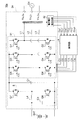
- FIG. 7 is a configuration diagram of the bidirectional power conditioner 10. As shown in the figure, the bidirectional power conditioner 10 includes a main circuit 1 a and a control unit 2.
- the main circuit 1a includes a bridge type conversion circuit 11, a current / voltage detection circuit 12, a reactor (L1, L2, L4), a capacitor (C1, C2), a bidirectional chopper circuit 5, and the like. Note that the configurations of the bridge type conversion circuit 11 and the current-voltage detection circuit 12 are the same as those of the first embodiment, and thus description thereof is omitted.
- the control unit 2 outputs the drive pulse signals (G1 to G4) so that the DC / AC conversion of the voltage is performed in the direction opposite to the direction of performing the AC / DC conversion. It also has a function to output.
- the main circuit 1a is connected to a power distribution system E3 that supplies single-phase AC power and a secondary battery BAT, so that bidirectional power transmission (charging and discharging of the secondary battery BAT) is possible.
- the main circuit 1a receives AC power (AC input current Ii and AC input voltage V ⁇ BR> sword J from the power distribution system E3, and DC power from the secondary battery BAT.
- the bidirectional chopper circuit 5 has switching elements (Q7, Q8), a reactor L4, and a capacitor C3.
- the emitter of switching element Q7 is connected to the collector of switching element Q8 and one end of reactor L4.
- the collector of the switching element Q7 is connected to the upper output end of the bridge type conversion circuit 11 and one end of the capacitor C1.
- the emitter of the switching element Q8 is connected to the lower output end of the bridge type conversion circuit 11, the other end of the capacitor C1, and the negative electrode side of the secondary battery BAT.
- the other end of the reactor L4 is connected to the positive electrode side of the secondary battery BAT.
- both ends of the capacitor C3 are connected to the positive electrode side and the negative electrode side of the secondary battery BAT, respectively.
- the bidirectional chopper circuit 5 receives a pulse signal from a control device (not shown), and the switching elements (Q7, Q8) perform switching in response thereto.
- the bidirectional chopper circuit 5 is either in the direction from the bridge type conversion circuit 11 side to the secondary battery BAT side or in the direction from the secondary battery BAT side to the bridge type conversion circuit 11 side (that is, bidirectional). It has a function of converting DC voltage (DC-DC conversion).
- the voltage conversion by the bidirectional chopper circuit 5 may be either step-up or step-down.
- connection point between the switching element Q3 and the switching element Q4 is connected to the positive side of the distribution system E3 via the reactor L1, and the connection point between the switching element Q1 and the switching element Q2 is the negative side of the distribution system E3. It is connected to the. Further, both ends of the capacitor C2 are connected to the positive electrode side and the negative electrode side of the power distribution system E3, respectively.
- the bidirectional power converter 10 performs AC-DC conversion by the bridge type conversion circuit 11 and a bidirectional chopper circuit with respect to the AC voltage (AC input voltage Vs) input from the distribution system E3 when charging the secondary battery BAT.
- Each switching element Q1 to Q4, O7, Q8) is controlled so that DC-DC conversion by 5 is performed in order.
- the bidirectional power conditioner 10 outputs the DC voltage obtained by these conversion operations to the secondary battery BAT.
- the direct current-DC conversion by the bidirectional chopper circuit 5 and the direct current by the bridge type conversion circuit 11 are applied to the DC voltage input from the secondary battery BAT. Control each switching element (Q1 to Q4, O7, Q8) so that AC conversion is performed in order.
- the bidirectional power conditioner 10 outputs the AC voltage obtained by these conversion operations to the power distribution system E3.
- the main circuit 1a has a two-stage configuration of the bridge type conversion circuit 11 and the bidirectional chopper circuit 5.
- the control procedure of the bridge type conversion circuit 11 at the time of charging the secondary battery BAT is as follows. This is the same as in the first embodiment.
- the modulation degree MV of the pulse width modulation performed by the control unit 2 operates so as to always be a value near 1 based on the same principle as in the first embodiment. Controlled.
- the bidirectional power converter 10 of the present embodiment is a power conversion device having a configuration substantially equivalent to that of the first embodiment (however, the voltage DC-AC is reversed in the direction opposite to the direction in which AC-DC conversion is performed. And a bidirectional chopper circuit 5, a power distribution system E 3 is connected to the power converter, and a secondary battery BAT is connected to the bidirectional chopper circuit 5. It can be seen as something like that.
- the bidirectional power conditioner 10 converts the alternating current voltage input to the power converter side into a direct current voltage obtained by sequentially performing alternating current-direct current conversion and direct current-direct current conversion of the bidirectional chopper circuit 5.
- the output from the power converter and the AC voltage obtained by sequentially performing DC-DC conversion and DC-AC conversion on the DC voltage input to the bidirectional chopper circuit 5 side are output from the power converter side. It can be said that it performs operation.
- the power converter 9a (high power factor converter) corresponding to a three-phase alternating current power supply was demonstrated as 2nd Embodiment.
- the structure form of the power converter device 9a it can utilize for the apparatus of various uses.
- a bi-directional power conditioner one form of a power conversion system for a secondary battery will be described as an example, and will be described below as a fourth embodiment.
- FIG. 8 is a configuration diagram of the bidirectional power conditioner 10a. As shown in the figure, the bidirectional power conditioner 10 a includes a main circuit 2 a and a control unit 4.
- the main circuit 2a includes a bridge type conversion circuit 31, a current / voltage detection circuit 32, a reactor (L1 to L4), a capacitor C1, and a bidirectional chopper circuit 5.
- the configurations of the bridge type conversion circuit 31 and the current / voltage detection circuit 32 are equivalent to those of the second embodiment, and the configuration of the bidirectional chopper circuit 5 is equivalent to that of the third embodiment. Each description is omitted.
- the control unit 4 outputs the drive pulse signals (G1 to G6) so that the DC / AC conversion of the voltage is performed in the direction opposite to the AC / DC conversion direction. It also has a function to output.
- the main circuit 2a is connected to a power distribution system E4 that supplies three-phase AC power and a secondary battery BAT, so that bidirectional power transmission (charging and discharging of the secondary battery BAT) is possible.
- the main circuit 2a receives AC power (AC input currents (Iu, Iv, Iw) and AC input voltages (Vu, Vv, Vw) of each phase) from the distribution system E4, and DC from the secondary battery BAT. Power is input.
- connection point between the switching element Q1 and the switching element Q2 is connected to the U-phase power supply line of the distribution system E4 via the reactor L1, and the connection point between the switching element Q3 and the switching element Q4 is connected via the reactor L2.
- the connection point between the switching element Q5 and the switching element Q6 is connected to the W-phase power supply line of the distribution system E4 via the reactor L3.
- the bidirectional power converter 10a When charging the secondary battery BAT, the bidirectional power converter 10a performs AC-DC conversion by the bridge type conversion circuit 31 and DC-DC conversion by the bidirectional chopper circuit 5 with respect to the AC voltage input from the distribution system E4.
- the switching elements (Q1 to Q8) are controlled so that the steps are sequentially performed.
- the bidirectional power conditioner 10a outputs the DC voltage obtained by these conversion operations to the secondary battery BAT.
- the DC voltage input from the secondary battery BAT is converted into DC / DC conversion by the bidirectional chopper circuit 5 and DC by the bridge type conversion circuit 31. Control each switching element (Q1 to Q8) so that AC conversion is performed in order.
- the bidirectional power conditioner 10a outputs the AC voltage obtained by these conversion operations to the power distribution system E4.
- the main circuit 2a has a two-stage configuration of the bridge type conversion circuit 31 and the bidirectional chopper circuit 5, but the control procedure of the bridge type conversion circuit 31 at the time of charging the secondary battery BAT This is the same as in the second embodiment.
- the modulation degree MD of the pulse width modulation performed by the control unit 4 operates so as to always be a value near 1 based on the same principle as in the second embodiment. Controlled.
- the bidirectional power converter 10a of the present embodiment is a power conversion device having a configuration substantially equivalent to that of the second embodiment (however, the voltage DC-AC in the direction opposite to the direction in which AC-DC conversion is performed).
- a bidirectional chopper circuit 5 a power distribution system E 4 is connected to the power converter, and a secondary battery BAT is connected to the bidirectional chopper circuit 5. It can be seen as something like that.
- the bidirectional power conditioner 10a converts the AC voltage input to the power converter side into a DC voltage obtained by sequentially performing AC-DC conversion and DC-DC conversion, and the bidirectional chopper circuit 5
- the output from the power converter and the AC voltage obtained by sequentially performing DC-DC conversion and DC-AC conversion on the DC voltage input to the bidirectional chopper circuit 5 side are output from the power converter side. It can be said that it performs operation.
- FIG. 9 is a configuration diagram of the motor inverter 6. As shown in the figure, the motor inverter 6 has a power converter 9 and a DC-AC converter circuit 7. The motor inverter 6 is used in a form in which a single-phase AC power source E1 that supplies single-phase AC power is connected to the input side, and a motor 8 that is driven by AC power is connected to the output side.
- a single-phase AC power source E1 that supplies single-phase AC power is connected to the input side
- a motor 8 that is driven by AC power is connected to the output side.
- the motor inverter 6 converts the AC voltage input from the single-phase AC power source E1 into a DC voltage by the power conversion device 9, and then converts the AC voltage into an AC voltage by the DC-AC conversion circuit 7 and outputs it to the motor 8. Then, the motor 8 is driven.
- the power converter device 9 since the power converter device 9 has a function as a high power factor converter, it plays a role of improving the power factor.
- the motor inverter 6 includes the power conversion device 9 and the DC-AC conversion circuit 7 that receives the DC voltage obtained by AC-DC conversion and performs DC-AC conversion on the DC voltage.
- the AC voltage obtained by this DC-AC conversion is output as a voltage for driving the motor.
- the power converter device 9a which concerns on 2nd Embodiment instead of the power converter device 9 as components for power factor improvement.
- the motor inverter 6 corresponds to a three-phase AC power source.
- the power conversion device includes a switching element that performs switching according to the drive pulse signal, and performs main-to-DC conversion on the input AC voltage by the switching.
- a circuit a function unit (operation signal generation unit) that generates an operation signal that determines an operation amount of the switching element, and pulse width modulation using the operation signal as a signal wave, and the drive pulse signal corresponding to the operation signal
- a function unit pulse signal generation unit
- the operation signal generation unit detects the modulation degree in the pulse width modulation, and generates the operation signal based on the detected value of the modulation degree. Therefore, according to the power conversion device according to each embodiment, a mechanism (such as a DC voltage detector) or operation for detecting or estimating a DC output voltage is not required, and an input current waveform is not distorted. In addition, it is easy to dynamically set the target value of the DC output voltage so that the efficiency of power conversion becomes sufficiently high. In addition, it is possible to perform more appropriate control of the output voltage that does not depend on errors in the detection circuit or variations in the elements of the main circuit, and that can dynamically follow fluctuations in the AC input voltage and load fluctuations in the power converter. Therefore, it is possible to realize a power conversion device that has less harmonic input current than the conventional one, is more efficient, and achieves downsizing and cost reduction.
- the operation signal generation unit feeds back a detection value of the modulation degree and generates an operation signal so that the modulation degree approaches a preset target value.
- other forms may be adopted as a form for reflecting the detected value in the generation of the operation signal, a specific form of feedback of the detected value, and the like without departing from the gist of the present invention. Absent. Further, instead of making the modulation degree approach the preset target value, a form of generating the operation signal may be adopted so that the modulation degree falls within the preset allowable range.
- the present invention can be used for a power converter that converts an AC voltage into a DC voltage.
Landscapes
- Engineering & Computer Science (AREA)
- Power Engineering (AREA)
- Inverter Devices (AREA)
- Rectifiers (AREA)
- Control Of Ac Motors In General (AREA)
- Dc-Dc Converters (AREA)
Abstract
L'invention concerne un dispositif de conversion de puissance électrique dans lequel une valeur cible pour une tension de sortie continue peut être facilement définie dynamiquement de sorte que le rendement de conversion de puissance électrique soit suffisamment élevé, sans distordre la forme d'onde du courant d'entrée et sans requérir un mécanisme ou des opérations servant à estimer ou détecter la tension de sortie continue. Un dispositif de conversion de puissance électrique comporte : un circuit de conversion, qui a un élément de commutation servant à effectuer une commutation en réponse à un signal d'impulsion de commande, et qui effectue une conversion CA-CC sur une tension alternative entrée, au moyen de la commutation ; une unité de génération de signal d'opération, qui génère un signal d'opération servant à déterminer la quantité opérationnelle de l'élément de commutation ; et une unité de génération de signal d'impulsion servant à effectuer une modulation de largeur d'impulsion dont une onde de signal est le signal d'opération, et générant un signal d'impulsion de commande en fonction du signal d'opération. L'unité de génération de signal d'opération détecte le degré de modulation dans la modulation de largeur d'impulsion, et génère le signal d'opération sur la base de la valeur détectée du degré de modulation.
Applications Claiming Priority (2)
| Application Number | Priority Date | Filing Date | Title |
|---|---|---|---|
| JP2011-041391 | 2011-02-28 | ||
| JP2011041391A JP2012178944A (ja) | 2011-02-28 | 2011-02-28 | 電力変換装置、電力変換システム、およびモータインバータ |
Publications (1)
| Publication Number | Publication Date |
|---|---|
| WO2012117642A1 true WO2012117642A1 (fr) | 2012-09-07 |
Family
ID=46757589
Family Applications (1)
| Application Number | Title | Priority Date | Filing Date |
|---|---|---|---|
| PCT/JP2011/078920 Ceased WO2012117642A1 (fr) | 2011-02-28 | 2011-12-14 | Dispositif de conversion de puissance électrique, système de conversion de puissance électrique, et inverseur moteur |
Country Status (2)
| Country | Link |
|---|---|
| JP (1) | JP2012178944A (fr) |
| WO (1) | WO2012117642A1 (fr) |
Cited By (6)
| Publication number | Priority date | Publication date | Assignee | Title |
|---|---|---|---|---|
| JP2016025746A (ja) * | 2014-07-18 | 2016-02-08 | 富士電機株式会社 | 電力貯蔵システム、電力変換装置、自立運転システム、及び電力貯蔵システムの制御方法 |
| JP2017112776A (ja) * | 2015-12-18 | 2017-06-22 | 三菱重工業株式会社 | コンバータ装置、駆動制御装置、モータ、およびコンプレッサ |
| JP2017123706A (ja) * | 2016-01-05 | 2017-07-13 | 東芝三菱電機産業システム株式会社 | 電力変換装置及びその制御方法 |
| JP2018007326A (ja) * | 2016-06-28 | 2018-01-11 | 日立ジョンソンコントロールズ空調株式会社 | 電力変換装置、及びこれを備える空気調和機 |
| CN113992240A (zh) * | 2021-10-26 | 2022-01-28 | 深圳智微电子科技有限公司 | 一种用于载波通信的调制系统及其控制方法 |
| JP2024509642A (ja) * | 2021-02-05 | 2024-03-04 | エイジャックス トッコ マグネサーミック コーポレーション | 誘導加熱溶解用途向けの電流源インバータ及び電圧源インバータを備えたアクティブ整流器電力システム |
Families Citing this family (2)
| Publication number | Priority date | Publication date | Assignee | Title |
|---|---|---|---|---|
| JP6087238B2 (ja) * | 2013-07-26 | 2017-03-01 | 株式会社日立情報通信エンジニアリング | 電源装置とその運転方法 |
| JP6528561B2 (ja) * | 2015-06-26 | 2019-06-12 | 富士電機株式会社 | 高効率力率改善回路およびスイッチング電源装置 |
Citations (3)
| Publication number | Priority date | Publication date | Assignee | Title |
|---|---|---|---|---|
| JPS63224671A (ja) * | 1987-03-10 | 1988-09-19 | Daikin Ind Ltd | 力率改善回路 |
| JPH1175372A (ja) * | 1997-08-29 | 1999-03-16 | High Frequency Heattreat Co Ltd | 電力変換装置及び電力変換方法 |
| JP2006006046A (ja) * | 2004-06-18 | 2006-01-05 | Daikin Ind Ltd | コンバータ制御方法及びコンバータ制御装置並びに空調機及びその制御方法及び制御装置 |
-
2011
- 2011-02-28 JP JP2011041391A patent/JP2012178944A/ja not_active Withdrawn
- 2011-12-14 WO PCT/JP2011/078920 patent/WO2012117642A1/fr not_active Ceased
Patent Citations (3)
| Publication number | Priority date | Publication date | Assignee | Title |
|---|---|---|---|---|
| JPS63224671A (ja) * | 1987-03-10 | 1988-09-19 | Daikin Ind Ltd | 力率改善回路 |
| JPH1175372A (ja) * | 1997-08-29 | 1999-03-16 | High Frequency Heattreat Co Ltd | 電力変換装置及び電力変換方法 |
| JP2006006046A (ja) * | 2004-06-18 | 2006-01-05 | Daikin Ind Ltd | コンバータ制御方法及びコンバータ制御装置並びに空調機及びその制御方法及び制御装置 |
Cited By (7)
| Publication number | Priority date | Publication date | Assignee | Title |
|---|---|---|---|---|
| JP2016025746A (ja) * | 2014-07-18 | 2016-02-08 | 富士電機株式会社 | 電力貯蔵システム、電力変換装置、自立運転システム、及び電力貯蔵システムの制御方法 |
| JP2017112776A (ja) * | 2015-12-18 | 2017-06-22 | 三菱重工業株式会社 | コンバータ装置、駆動制御装置、モータ、およびコンプレッサ |
| JP2017123706A (ja) * | 2016-01-05 | 2017-07-13 | 東芝三菱電機産業システム株式会社 | 電力変換装置及びその制御方法 |
| JP2018007326A (ja) * | 2016-06-28 | 2018-01-11 | 日立ジョンソンコントロールズ空調株式会社 | 電力変換装置、及びこれを備える空気調和機 |
| JP7044462B2 (ja) | 2016-06-28 | 2022-03-30 | 日立ジョンソンコントロールズ空調株式会社 | 電力変換装置、及びこれを備える空気調和機 |
| JP2024509642A (ja) * | 2021-02-05 | 2024-03-04 | エイジャックス トッコ マグネサーミック コーポレーション | 誘導加熱溶解用途向けの電流源インバータ及び電圧源インバータを備えたアクティブ整流器電力システム |
| CN113992240A (zh) * | 2021-10-26 | 2022-01-28 | 深圳智微电子科技有限公司 | 一种用于载波通信的调制系统及其控制方法 |
Also Published As
| Publication number | Publication date |
|---|---|
| JP2012178944A (ja) | 2012-09-13 |
Similar Documents
| Publication | Publication Date | Title |
|---|---|---|
| EP3522355B1 (fr) | Dispositif de commande pour convertisseur de puissance directe | |
| EP1814215B1 (fr) | Convertisseur de puissance électrique et système de commande de moteur | |
| US9882466B2 (en) | Power conversion device including an AC/DC converter and a DC/DC converter | |
| US8564261B2 (en) | Power converting apparatus, grid interconnection apparatus and grid interconnection system | |
| WO2012117642A1 (fr) | Dispositif de conversion de puissance électrique, système de conversion de puissance électrique, et inverseur moteur | |
| US8084986B2 (en) | Dead-time compensation apparatus of PWM inverter and method thereof | |
| CN103650333B (zh) | 车辆和车辆的控制方法 | |
| JP5316514B2 (ja) | 電力変換装置 | |
| EP2372894B1 (fr) | Système inverseur de courant continu à courant alternatif triphasique | |
| EP3422551A1 (fr) | Dispositif de conversion de puissance, dispositif d'entraînement de moteur et réfrigérateur l'utilisant | |
| US10523128B1 (en) | Reactive AFE power control | |
| CN100574090C (zh) | 电功率转换设备 | |
| US20110241587A1 (en) | Direct-current to three-phase alternating-current inverter system | |
| WO2017119214A1 (fr) | Dispositif de conversion d'énergie électrique | |
| JP5321282B2 (ja) | 電力制御装置 | |
| JP2011109803A (ja) | 電動機の制御装置 | |
| JP5407553B2 (ja) | モータ制御装置 | |
| JP2020115719A (ja) | 電力制御方法、及び、電力制御装置 | |
| JP4797371B2 (ja) | 電力変換装置の制御方法 | |
| JP5338853B2 (ja) | 電力変換装置 | |
| JP2007282405A (ja) | 電力変換装置 | |
| JP2006166628A (ja) | 電力変換装置の制御方法 | |
| JP2007068296A (ja) | 電力変換装置 | |
| JP5334920B2 (ja) | 負荷駆動装置 | |
| JP2010028941A (ja) | 回転機の制御装置 |
Legal Events
| Date | Code | Title | Description |
|---|---|---|---|
| 121 | Ep: the epo has been informed by wipo that ep was designated in this application |
Ref document number: 11860061 Country of ref document: EP Kind code of ref document: A1 |
|
| NENP | Non-entry into the national phase |
Ref country code: DE |
|
| 122 | Ep: pct application non-entry in european phase |
Ref document number: 11860061 Country of ref document: EP Kind code of ref document: A1 |