WO2012117775A1 - Module de cellule solaire et procédé de fabrication de module de cellule solaire - Google Patents
Module de cellule solaire et procédé de fabrication de module de cellule solaire Download PDFInfo
- Publication number
- WO2012117775A1 WO2012117775A1 PCT/JP2012/051616 JP2012051616W WO2012117775A1 WO 2012117775 A1 WO2012117775 A1 WO 2012117775A1 JP 2012051616 W JP2012051616 W JP 2012051616W WO 2012117775 A1 WO2012117775 A1 WO 2012117775A1
- Authority
- WO
- WIPO (PCT)
- Prior art keywords
- solar cell
- cell module
- mark
- light
- resin sealing
- Prior art date
- Legal status (The legal status is an assumption and is not a legal conclusion. Google has not performed a legal analysis and makes no representation as to the accuracy of the status listed.)
- Ceased
Links
Images
















Classifications
-
- H—ELECTRICITY
- H10—SEMICONDUCTOR DEVICES; ELECTRIC SOLID-STATE DEVICES NOT OTHERWISE PROVIDED FOR
- H10F—INORGANIC SEMICONDUCTOR DEVICES SENSITIVE TO INFRARED RADIATION, LIGHT, ELECTROMAGNETIC RADIATION OF SHORTER WAVELENGTH OR CORPUSCULAR RADIATION
- H10F77/00—Constructional details of devices covered by this subclass
-
- H—ELECTRICITY
- H10—SEMICONDUCTOR DEVICES; ELECTRIC SOLID-STATE DEVICES NOT OTHERWISE PROVIDED FOR
- H10F—INORGANIC SEMICONDUCTOR DEVICES SENSITIVE TO INFRARED RADIATION, LIGHT, ELECTROMAGNETIC RADIATION OF SHORTER WAVELENGTH OR CORPUSCULAR RADIATION
- H10F19/00—Integrated devices, or assemblies of multiple devices, comprising at least one photovoltaic cell covered by group H10F10/00, e.g. photovoltaic modules
- H10F19/30—Integrated devices, or assemblies of multiple devices, comprising at least one photovoltaic cell covered by group H10F10/00, e.g. photovoltaic modules comprising thin-film photovoltaic cells
- H10F19/31—Integrated devices, or assemblies of multiple devices, comprising at least one photovoltaic cell covered by group H10F10/00, e.g. photovoltaic modules comprising thin-film photovoltaic cells having multiple laterally adjacent thin-film photovoltaic cells deposited on the same substrate
-
- H—ELECTRICITY
- H10—SEMICONDUCTOR DEVICES; ELECTRIC SOLID-STATE DEVICES NOT OTHERWISE PROVIDED FOR
- H10F—INORGANIC SEMICONDUCTOR DEVICES SENSITIVE TO INFRARED RADIATION, LIGHT, ELECTROMAGNETIC RADIATION OF SHORTER WAVELENGTH OR CORPUSCULAR RADIATION
- H10F19/00—Integrated devices, or assemblies of multiple devices, comprising at least one photovoltaic cell covered by group H10F10/00, e.g. photovoltaic modules
- H10F19/30—Integrated devices, or assemblies of multiple devices, comprising at least one photovoltaic cell covered by group H10F10/00, e.g. photovoltaic modules comprising thin-film photovoltaic cells
- H10F19/31—Integrated devices, or assemblies of multiple devices, comprising at least one photovoltaic cell covered by group H10F10/00, e.g. photovoltaic modules comprising thin-film photovoltaic cells having multiple laterally adjacent thin-film photovoltaic cells deposited on the same substrate
- H10F19/33—Patterning processes to connect the photovoltaic cells, e.g. laser cutting of conductive or active layers
-
- H—ELECTRICITY
- H10—SEMICONDUCTOR DEVICES; ELECTRIC SOLID-STATE DEVICES NOT OTHERWISE PROVIDED FOR
- H10F—INORGANIC SEMICONDUCTOR DEVICES SENSITIVE TO INFRARED RADIATION, LIGHT, ELECTROMAGNETIC RADIATION OF SHORTER WAVELENGTH OR CORPUSCULAR RADIATION
- H10F19/00—Integrated devices, or assemblies of multiple devices, comprising at least one photovoltaic cell covered by group H10F10/00, e.g. photovoltaic modules
- H10F19/80—Encapsulations or containers for integrated devices, or assemblies of multiple devices, having photovoltaic cells
-
- H—ELECTRICITY
- H10—SEMICONDUCTOR DEVICES; ELECTRIC SOLID-STATE DEVICES NOT OTHERWISE PROVIDED FOR
- H10F—INORGANIC SEMICONDUCTOR DEVICES SENSITIVE TO INFRARED RADIATION, LIGHT, ELECTROMAGNETIC RADIATION OF SHORTER WAVELENGTH OR CORPUSCULAR RADIATION
- H10F77/00—Constructional details of devices covered by this subclass
- H10F77/93—Interconnections
- H10F77/933—Interconnections for devices having potential barriers
- H10F77/935—Interconnections for devices having potential barriers for photovoltaic devices or modules
- H10F77/937—Busbar structures for modules
-
- H—ELECTRICITY
- H10—SEMICONDUCTOR DEVICES; ELECTRIC SOLID-STATE DEVICES NOT OTHERWISE PROVIDED FOR
- H10F—INORGANIC SEMICONDUCTOR DEVICES SENSITIVE TO INFRARED RADIATION, LIGHT, ELECTROMAGNETIC RADIATION OF SHORTER WAVELENGTH OR CORPUSCULAR RADIATION
- H10F77/00—Constructional details of devices covered by this subclass
- H10F77/93—Interconnections
- H10F77/933—Interconnections for devices having potential barriers
- H10F77/935—Interconnections for devices having potential barriers for photovoltaic devices or modules
- H10F77/939—Output lead wires or elements
-
- Y—GENERAL TAGGING OF NEW TECHNOLOGICAL DEVELOPMENTS; GENERAL TAGGING OF CROSS-SECTIONAL TECHNOLOGIES SPANNING OVER SEVERAL SECTIONS OF THE IPC; TECHNICAL SUBJECTS COVERED BY FORMER USPC CROSS-REFERENCE ART COLLECTIONS [XRACs] AND DIGESTS
- Y02—TECHNOLOGIES OR APPLICATIONS FOR MITIGATION OR ADAPTATION AGAINST CLIMATE CHANGE
- Y02E—REDUCTION OF GREENHOUSE GAS [GHG] EMISSIONS, RELATED TO ENERGY GENERATION, TRANSMISSION OR DISTRIBUTION
- Y02E10/00—Energy generation through renewable energy sources
- Y02E10/50—Photovoltaic [PV] energy
Definitions
- the present invention relates to a solar cell module including a solar cell portion between two light-transmitting substrates, and a method for manufacturing the solar cell module.
- Solar cell modules are international products related to display / safety because they are electrical products, there is demand in the global market, and safety is particularly important because they are used at home, and other related standards.
- a predetermined display along the line is required. Specifically, it is required to display information defined by various standards on the product body of the solar cell module.
- a nameplate is used as a means of displaying information necessary for electrical products and is attached to the product body. However, since it is necessary to improve the light receiving efficiency (power generation efficiency) as much as possible in the solar cell module, it is avoided to attach the nameplate to the surface side irradiated with sunlight.
- the solar cell module when attaching to the back side of the solar cell module, it may be difficult to attach the nameplate depending on the structure of the back side.
- the nameplate When the nameplate is attached to the back surface of the solar cell module, the solar cell module is installed outdoors, and may be rubbed by an object disposed in the vicinity.
- the information (display contents) described on the nameplate may not be recognized due to the occurrence of scratches, dirt, etc.
- the surface of the nameplate may be deteriorated and deformed (discolored) by being exposed to wind and rain due to long-term installation, and the contents of the nameplate may not be recognized.
- a solar cell module in which a mark is formed by laser processing at a certain depth from the light receiving surface in the non-power generation region of the light transmitting substrate on the surface side (for example, a patent) Reference 1).
- Recent solar cell modules are required to make the non-power generation region as small as possible in order to increase power generation efficiency. Therefore, it is difficult to form a nameplate that displays all the items based on the standard in the non-power generation region, and there is a problem that a region for forming a mark cannot be secured in the non-power generation region. Moreover, when forming a required nameplate in a non-power generation area
- This invention is made
- the purpose of the present invention is to provide a solar cell module that can prevent the influence of the power generation, improve the mechanical strength of the mark portion in a state where the reduction in the amount of power generation is prevented, and improve the durability, weather resistance, and reliability. To do.
- this invention is a manufacturing method of the solar cell module which concerns on this invention, Comprising: The range of the area
- the solar cell module according to the present invention is a solar cell module in which a first translucent substrate, a solar cell unit, a resin sealing unit, and a second translucent substrate are arranged in this order from the sunlight irradiation side. And it is provided with the mark part formed between the boundary of the said solar cell part and the said resin sealing part, and the outer surface of a said 2nd translucent board
- the solar cell module according to the present invention forms (arranges) a mark portion having a high recognition rate between the boundary between the solar cell portion and the resin sealing portion and the outer surface of the second translucent substrate in the thickness direction. Therefore, in the plane direction, it can be formed (arranged) without being restricted to the power generation region, so that it is possible to prevent the influence on the power generation region (power generation amount) and the influence on the mark part from the outside.
- the mechanical strength of the mark portion is improved in a state where the reduction of the deterioration is prevented, and durability, weather resistance, and reliability are improved.
- the solar cell module according to the present invention is characterized in that the mark portion is formed in the resin sealing portion.
- the solar cell module according to the present invention can easily recognize the information displayed on the mark part as compared with the case where the mark part is arranged on the second light-transmitting substrate. , Weather resistance and reliability can be maintained.
- the solar cell module according to the present invention is characterized in that the resin sealing portion uses black ionomer resin as a sealing resin.
- the solar cell module according to the present invention forms the resin sealing portion with a black ionomer resin, the heat absorption property to the laser at the resin sealing portion is improved, so that the discoloration of the ionomer resin is effectively realized.
- the mark portion can display the information with high accuracy.
- the solar cell module according to the present invention is characterized in that the sealing resin contains carbon black.
- the solar cell module according to the present invention contains carbon black in the resin sealing portion (sealing resin), the mark that effectively generates the discoloration of the carbon black by the laser and displays the information more clearly.
- the recognition rate is improved in both visual recognition and automatic recognition using a camera or the like.
- the solar cell module according to the present invention is characterized in that the mark portion is formed in an embedded member embedded in the resin sealing portion.
- the solar cell module according to the present invention produces the mark portion on the embedded member embedded in the resin sealing portion even when the temperature resistance of the sealing resin forming the resin sealing portion is not sufficient. And reliability can be improved.
- the solar cell module according to the present invention is characterized in that the font of letters formed on the mark portion is in a form that excludes the intersection.
- the solar cell module according to the present invention suppresses heat generation due to laser processing even when the mark portion is formed by laser processing, compared to when the crossing portion is present, Occurrence can be prevented.
- the solar cell module according to the present invention is characterized in that the mark portion is formed on the second light transmitting substrate.
- the solar cell module according to the present invention can form a mark portion having high temperature resistance because the mark portion is formed on the second light-transmitting substrate.
- the solar cell module according to the present invention is characterized in that the mark portion is arranged on the outer surface side with respect to the center of the thickness of the second translucent substrate.
- the solar cell module according to the present invention arranges the mark portion on the outer surface side from the center of the thickness of the second translucent substrate, so that the resin sealing portion and the sun when forming the mark portion are arranged. It is possible to improve the yield by suppressing the influence on the battery part and preventing the resin sealing part and the solar battery part from being damaged.
- the solar cell module according to the present invention is characterized in that the mark portion displays information as a nameplate.
- the solar cell module according to the present invention includes a mark portion indicating information (for example, a manufacturer) as a nameplate in a form that protects from the outside, the nameplate information can be displayed without attaching the nameplate. Improve product reliability and ease of handling.
- the solar cell module according to the present invention is characterized in that the mark portion displays information on electrical characteristics.
- the solar cell module according to the present invention can display information on electrical characteristics (electrical specifications) without attaching a nameplate, the reliability of the product and the ease of handling are improved.
- the solar cell module according to the present invention is characterized in that the mark portion includes a display by a two-dimensional code.
- the solar cell module according to the present invention can be automatically read using a code reader that reads a two-dimensional code, it is possible to improve the efficiency of handling, maintenance, and the like.
- the solar cell unit is formed of a thin film solar cell
- the thin film solar cell is formed of a transparent electrode layer, a photoelectric conversion layer, and a back surface from the first translucent substrate side.
- the electrode layers are laminated in this order.
- the solar cell module according to the present invention is constituted by a thin film solar cell, the material necessary for the solar cell unit can be suppressed and the productivity can be improved.
- the first translucent substrate, the solar cell unit, the resin sealing unit, and the second translucent substrate are arranged in this order from the sunlight irradiation side.
- a method for manufacturing a battery module comprising irradiating a light beam through the second light transmissive substrate to a boundary between the solar cell portion and the resin sealing portion to an outer surface of the second light transmissive substrate. A mark portion is formed between them.
- the manufacturing method of the solar cell module according to the present invention can easily provide a mark portion with a high recognition rate between the boundary between the solar cell portion and the resin sealing portion and the outer surface of the second light transmissive substrate. Since it can be formed (arranged) with high accuracy, a solar cell module having high durability, weather resistance and reliability can be manufactured with high productivity.
- the resin sealing portion contains carbon black, and the light beam discolors the carbon black and displays information on the mark portion.
- the mark portion is formed by irradiating the light beam to discolor the carbon black, so that the mark portion with a high recognition rate can be formed.
- the light beam is generated by an SHG laser.
- the method of manufacturing the solar cell module according to the present invention generates the light beam by the SHG laser, it is possible to suppress the generation of heat and prevent the generation of bubbles and improve the quality.
- the solar cell module includes the mark portion formed between the boundary between the solar cell portion and the resin sealing portion and the outer surface of the second translucent substrate. Quantity) and external influences on the mark part can be prevented, and the mechanical strength of the mark part is improved in a state where the reduction in power generation is prevented, and durability, weather resistance, and reliability are improved. There is an effect of improving.
- the light beam is irradiated through the second light transmissive substrate to the outer surface of the second light transmissive substrate from the boundary between the solar cell portion and the resin sealing portion. Since the mark part is formed between the two, the mark part with a high recognition rate can be formed (placed) easily and with high accuracy, so that a solar cell module having high durability, weather resistance and reliability can be obtained. There is an effect that it can be manufactured with high productivity.
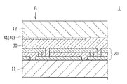
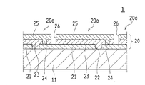
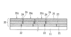
- FIG. 1 is an enlarged cross-sectional view showing an essential part of the solar cell module according to Embodiment 1 of the present invention.
- FIG. 2A is an enlarged cross-sectional view showing an essential part of the solar cell module according to Embodiment 2 of the present invention.
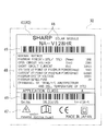
- FIG. 2B is an enlarged plan view showing the display state of the nameplate formed on the mark portion of the solar cell module viewed in the direction of arrow B in FIG. 2A.
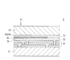
- FIG. 3A is an enlarged cross-sectional view illustrating a main part of the solar cell module according to Embodiment 3 of the present invention.
- FIG. 3B is an enlarged plan view showing the display state of the nameplate formed on the mark portion of the solar cell module viewed in the direction of arrow B in FIG. 3A.
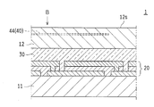
- FIG. 4A is an enlarged cross-sectional view showing an essential part of the solar cell module according to Embodiment 4 of the present invention.
- FIG. 4B is an enlarged plan view showing the display state of the nameplate formed on the mark portion of the solar cell module viewed in the direction of arrow B in FIG. 4A.
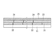
- FIG. 5A is an enlarged cross-sectional view illustrating an enlarged state of a main part in which a solar cell unit (thin film solar cell) is formed on a first light-transmitting substrate in the solar cell module according to Embodiment 5 of the present invention.
- FIG. 4A is an enlarged cross-sectional view showing an essential part of the solar cell module according to Embodiment 4 of the present invention.
- FIG. 4B is an enlarged plan view showing the display state of the nameplate formed on the mark portion of the solar cell module viewed in the direction of arrow B in FIG. 4A.
- FIG. 5A is an enlarged cross-sectional view illustrating an enlarged state of a main
- FIG. 5B is an exploded perspective view showing an exploded view of the insulating sheet forming the resin sealing portion in the solar cell module according to Embodiment 5 of the present invention and the second translucent substrate laminated on the insulating sheet.
- FIG. 5C is a perspective view showing a state in which the resin-sealed portion is formed by laminating the first light-transmitting substrate and the second light-transmitting substrate in the solar cell module according to Embodiment 5 of the present invention.
- FIG. 5D is a plan view showing an appearance on the second light-transmissive substrate side after the terminal box and the mark portion are formed in the solar cell module according to Embodiment 5 of the present invention.
- FIG. 6A is a schematic plan view showing a schematic state of the solar cell module according to Embodiment 6 of the present invention on the first light transmitting substrate side.
- FIG. 6B is a schematic plan view showing a schematic state on the second light transmitting substrate side of the solar cell module according to Embodiment 6 of the present invention.
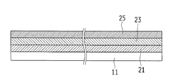
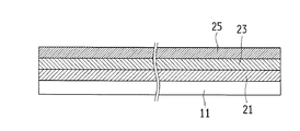
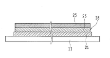
- FIG. 7A is a cross-sectional view showing a cross section when a transparent electrode layer is laminated on the first light-transmitting substrate in the manufacturing process of the solar cell module as seen in the direction of arrows AA in FIG. 6A.
- FIG. 7B is a cross-sectional view showing a cross section when a transparent electrode layer is laminated on the first light-transmitting substrate in the manufacturing process of the solar cell module seen in the direction of arrow BB in FIG. 6A.
- FIG. 8A is a cross-sectional view showing a cross section when the transparent electrode layer is separated by the first separation groove in the manufacturing process of the solar cell module as seen in the direction of arrows AA in FIG. 6A.
- FIG. 8B is a cross-sectional view showing a cross section when the transparent electrode layer is separated by the first separation groove in the manufacturing process of the solar cell module as seen in the direction of arrow BB in FIG. 6A.
- FIG. 8A is a cross-sectional view showing a cross section when the transparent electrode layer is separated by the first separation groove in the manufacturing process of the solar cell module as seen in the direction of arrow BB in FIG. 6A.
- FIG. 9A is a cross-sectional view showing a cross section when the photoelectric conversion layer is formed in the manufacturing process of the solar cell module as viewed in the direction of arrows AA in FIG. 6A.
- FIG. 9B is a cross-sectional view showing a cross section when the photoelectric conversion layer is formed in the manufacturing process of the solar cell module as seen in the direction of arrow BB in FIG. 6A.
- 10A is a cross-sectional view showing a cross section when a contact line is formed in the manufacturing process of the solar cell module as seen in the direction of arrow AA in FIG. 6A.
- FIG. 10B is a cross-sectional view showing a cross section when the contact line is formed in the manufacturing process of the solar cell module as seen in the direction of arrow BB in FIG.
- FIG. 11A is a cross-sectional view showing a cross section when the back electrode layer is formed in the manufacturing process of the solar cell module as seen in the direction of arrows AA in FIG. 6A.
- FIG. 11B is a cross-sectional view showing a cross section when the back electrode layer is formed in the manufacturing process of the solar cell module as seen in the direction of arrow BB in FIG. 6A.
- FIG. 12A is a cross-sectional view showing a cross section when the second separation groove is formed in the manufacturing process of the solar cell module as seen in the direction of arrows AA in FIG. 6A.
- FIG. 12B is a cross-sectional view showing a cross section when the second separation groove is formed in the manufacturing process of the solar cell module as seen in the direction of arrow BB in FIG. 6A.
- FIG. 13A is a cross-sectional view showing a cross section when the peripheral groove is formed in the manufacturing process of the solar cell module as seen in the direction of arrows AA in FIG. 6A.
- FIG. 13B is a cross-sectional view showing a cross section when the peripheral groove is formed in the manufacturing process of the solar cell module viewed in the direction of arrow BB in FIG. 6A.
- 14A is a cross-sectional view showing a cross section when an insulating isolation region is formed in the manufacturing process of the solar cell module as seen in the direction of arrow AA in FIG.
- FIG. 14B is a cross-sectional view showing a cross section when the insulating isolation region is formed in the manufacturing process of the solar cell module as seen in the direction of arrow BB in FIG. 6A.
- FIG. 15A is a cross-sectional view showing a cross section when a collecting electrode is formed in the manufacturing process of the solar cell module as seen in the direction of arrows AA in FIG. 6A.
- FIG. 15B is a cross-sectional view showing a cross section when the collecting electrode is formed in the manufacturing process of the solar cell module as seen in the direction of arrow BB in FIG. 6A.
- FIG. 14B is a cross-sectional view showing a cross section when the insulating isolation region is formed in the manufacturing process of the solar cell module as seen in the direction of arrow BB in FIG. 6A.
- FIG. 15A is a cross-sectional view showing a cross section when a collecting electrode is formed in the manufacturing process of the solar cell module as seen in the direction of arrow BB in FIG.
- FIG. 16A is a cross-sectional view showing a cross section when the resin sealing portion and the second light-transmitting substrate are laminated and bonded in the manufacturing process of the solar cell module viewed in the direction of arrows AA in FIG. 6A.
- FIG. 16B is a cross-sectional view showing a cross section when the resin sealing portion and the second light-transmitting substrate are laminated and bonded in the manufacturing process of the solar cell module as seen in the direction of arrow BB in FIG. 6A.
- FIG. 17A is a cross-sectional view showing a cross section when the mark portion is formed in the manufacturing process of the solar cell module as seen in the direction of arrows AA in FIG. 6A.
- FIG. 17B is a cross-sectional view showing a cross section when the mark portion is formed in the manufacturing process of the solar cell module 1 as seen in the direction of arrow BB in FIG. 6A.
- FIG. 17C is a plan view showing a state of bubbles generated when the formation condition of the mark portion is changed in FIG. 17A.
- 18A is a cross-sectional view showing a cross section when the mark portion is formed in the manufacturing process of the solar cell module as seen in the direction of arrows AA in FIG. 6A.
- 18B is a cross-sectional view showing a cross section when the mark portion is formed in the manufacturing process of the solar cell module as seen in the direction of arrow BB in FIG. 6A.
- FIG. 19A is a cross-sectional view showing a cross section when the mark portion is formed in the manufacturing process of the solar cell module as seen in the direction of arrows AA in FIG. 6A.
- FIG. 19B is a cross-sectional view showing a cross section when the mark portion is formed in the manufacturing process of the solar cell module as seen in the direction of arrow BB in FIG. 6A.
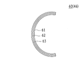
- FIG. 20A is a schematic diagram showing a laser beam processing unit for character A formed on the mark unit of the solar cell module according to Embodiment 9 of the present invention.
- FIG. 20B is a schematic diagram showing a laser beam processing unit for character B formed in the mark unit of the solar cell module according to Embodiment 9 of the present invention.
- FIG. 20C is a schematic diagram showing a laser beam processing unit for character C formed on the mark unit of the solar cell module according to Embodiment 9 of the present invention.
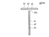
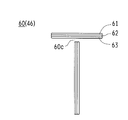
- FIG. 20D is a schematic diagram showing a laser beam processing unit for the letter T formed in the mark unit of the solar cell module according to Embodiment 9 of the present invention.
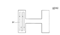
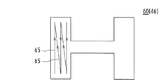
- FIG. 21A is a schematic diagram showing a laser beam processing unit when a wide character H formed on the mark unit of the solar cell module according to Embodiment 9 of the present invention is processed by a reciprocating scanning line.
- FIG. 21B is a schematic diagram showing a laser beam processing unit when a wide character H formed in the mark unit of the solar cell module according to Embodiment 9 of the present invention is processed by parallel scanning lines.
- FIG. 21C is a schematic diagram illustrating a laser beam processing unit when processing is performed by omitting the character outline of the wide character A formed in the mark unit of the solar cell module according to Embodiment 9 of the present invention.
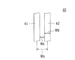
- FIG. 22A shows a first scanning line and a second scanning line when laser processing is performed by scanning a plurality of laser beams in parallel when forming the mark portion of the solar cell module according to Embodiment 9 of the present invention. It is a schematic diagram which shows typically this relationship.
- FIG. 22B shows a case where the letter T is laser processed by bringing the first scanning line through the third scanning line of the laser light into close contact with each other when forming the mark portion of the solar cell module according to Embodiment 9 of the present invention.
- FIG. 22C shows a case where the letter T is laser processed by separating the first to third scanning lines of the laser light from each other when forming the mark portion of the solar cell module according to Embodiment 9 of the present invention. It is a schematic diagram which shows typically the laser beam processing part.
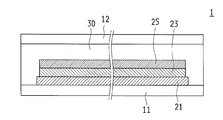
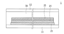
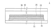
- FIG. 1 is an enlarged cross-sectional view showing an essential part of a solar cell module 1 according to Embodiment 1 of the present invention.
- the first translucent substrate 11, the solar cell unit 20, the resin sealing unit 30, and the second translucent substrate 12 are arranged in this order from the sunlight irradiation side. Arranged (laminated).
- the solar cell module 1 includes a mark portion 40 (specifically, a mark portion) formed between the boundary 30b between the solar cell portion 20 and the resin sealing portion 30 and the outer surface 12s of the second translucent substrate 12. Formed in a partial region within the range of the formation region 40r. Since a specific example of the mark unit 40 will be described in the second to fourth embodiments and the like, FIG. 1 shows an example corresponding to the second embodiment with an imaginary line (two-dot chain line).
- the solar cell module 1 has a recognition rate between the boundary 30b between the solar cell unit 20 and the resin sealing unit 30 and the outer surface 12s of the second light transmissive substrate 12 in the thickness direction. Since the high mark portion 40 is formed (arranged), it can be formed (arranged) in the plane direction without being restricted to the power generation region, and therefore the influence on the power generation region (power generation amount) and the influence on the mark portion 40 from the outside. In this state, the mechanical strength of the mark portion 40 is improved in a state in which a reduction in the amount of power generation is prevented, and durability, weather resistance, and reliability are improved.
- the mark portion 40 is placed at a position that does not affect power generation inside the solar cell module 1 (between the outer surface 12s of the second light-transmissive substrate 12 and the boundary 30b). Since it is in the enclosed form, it is possible to eliminate the influence from the outside without reducing the power generation amount, and to improve the durability, weather resistance, and reliability.
- substrate 12 are comprised, for example with the glass plate, and the solar cell part 20 was directly laminated
- the mark part 40 preferably displays information as a nameplate. That is, since the solar cell module 1 according to the present embodiment includes the mark portion 40 indicating information (for example, a manufacturer) as a nameplate in a form that protects it from the outside, the nameplate information can be obtained without attaching the nameplate. Since it can be displayed, the reliability of the product and the ease of handling are improved.
- the mark portion 40 formed as a nameplate nameplate information display example
- the mark part 40 is shown as a mark part 41 (see FIG. 2A) in the second embodiment, as a mark part 43 (see FIG. 3A) in the third embodiment, and as a mark part 44 (see FIG. 4A) in the fourth embodiment.
- the mark portion 41, the mark portion 43, and the mark portion 44 may be simply referred to as the mark portion 40 when it is not necessary to particularly distinguish them.
- the solar cell part 20 is comprised with the thin film solar cell.
- a transparent electrode layer 21, a photoelectric conversion layer 23, and a back electrode layer 25 are laminated in this order from the first light-transmissive substrate 11 side. Therefore, since the solar cell module 1 which concerns on this Embodiment comprises the solar cell part 20 by a thin film solar cell, it can suppress the material required for the solar cell part 20, and can improve productivity.
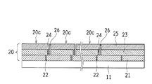
- FIG. 1 schematically shows another solar cell element portion 20c arranged (in series connection) adjacent to one solar cell element portion 20c.
- the solar cell element portion 20 c is separated from the other adjacent solar cell element portions 20 c by the first separation groove 22 and the second separation groove 26. Further, it is connected in series with another solar cell element portion 20 c arranged adjacent to the contact line 24.
- the first separation groove 22 is formed in the transparent electrode layer 21 and defines a basic region (region division) of the solar cell element portion 20c.
- the contact line 24 is formed so that the back electrode layer 25 is connected to the transparent electrode layer 21 on either side of the first separation groove 22 disposed on both sides of the transparent electrode layer 21, and is transparent to the back electrode layer 25. This is a connection path to the electrode layer 21.
- the second separation groove 26 is disposed adjacent to the contact line 24 and is formed so as to separate the photoelectric conversion layer 23 and the back electrode layer 25 from the photoelectric conversion layer 23 and the back electrode layer 25 of the adjacent solar cell element part 20c. Is done.
- the solar cell element portion 20c is formed in a strip shape, and is connected in series via the contact line 24 between the mutually adjacent ones.
- the solar cell module 1 that generates a high voltage is configured by the series connection of the solar cell element portions 20c.
- the specific example which comprises the solar cell module part 1 by connecting the solar cell element part 20c in series is further demonstrated in Embodiment 5.
- FIG. 5 The specific example which comprises the solar cell module part 1 by connecting the solar cell element part 20c in series is further demonstrated in Embodiment 5.
- the method for manufacturing the solar cell module 1 according to the present embodiment irradiates a light beam (not shown) through the second translucent substrate 12 to start from the boundary 30b between the solar cell unit 20 and the resin sealing unit 30.
- the manufacturing method of the solar cell module 1 according to the present embodiment has a recognition rate between the boundary 30b between the solar cell unit 20 and the resin sealing unit 30 and the outer surface 12s of the second light transmissive substrate 12. Since the high mark portion 40 can be formed (arranged) easily and with high accuracy, the solar cell module 1 having high durability, weather resistance, and reliability can be manufactured with high productivity.
- the step of forming the mark portion 40 is performed by laminating (adhering) the second light transmissive substrate 12 to the first light transmissive substrate 11, the solar cell portion 20, and the resin sealing portion 30. This is performed by irradiating a light beam (for example, a laser beam) from the outside after forming the solar cell module 1 with resin sealed inside.
- a light beam for example, a laser beam
- the member Since the light beam heats (absorbs heat) the member disposed at the focal position, the member can be denatured (discolored, decolored, clouded, etc.) to form a highly visible mark portion.
- the focal position of the light beam can be defined parallel to the first translucent substrate 11 and the like at an appropriate position of the resin sealing portion 30 in the thickness direction of the solar cell module 1.
- the planar mark part 40 can be formed corresponding to the (resin sealing part 30).
- the solar cell module 1 according to the present embodiment and the method for manufacturing the solar cell module 1 include other embodiments as a concept, and specific examples according to the present embodiment will be described in the other embodiments, respectively. Is done. The details of the method for manufacturing the solar cell module 1 will be further described in the fifth embodiment and thereafter.
- Embodiment 2 With reference to FIG. 2A and FIG. 2B, the solar cell module which concerns on this Embodiment, and the manufacturing method of a solar cell module are demonstrated. Since the basic configuration is the same as that of the first embodiment, the reference numerals are appropriately used and different items will be mainly described. In addition, about the manufacturing method of the solar cell module 1 which concerns on this Embodiment, Embodiment 6 demonstrates further detail.
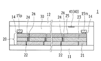
- FIG. 2A is an enlarged cross-sectional view showing an essential part of solar cell module 1 according to Embodiment 2 of the present invention.
- FIG. 2B is an enlarged plan view showing the display state of the nameplate formed on the mark portion 41 (mark portion 40) of the solar cell module 1 viewed in the direction of arrow B in FIG. 2A.
- the mark portion 41 (mark portion 40) is formed in the resin sealing portion 30. Therefore, the solar cell module 1 can easily recognize the information displayed on the mark part 41 as compared with the case where the mark part 40 is arranged on the second light-transmissive substrate 12 (see the fourth embodiment).
- the rate (visibility) can be improved and durability, weather resistance, and reliability can be maintained.
- Resin sealing portion 30 is formed by the following method. That is, after the solar cell portion 20 is formed in a laminated state on the first translucent substrate 11, a black ionomer resin containing carbon black (black carbon) (the metal ions between the molecules of the ethylene methacrylic acid copolymer) A cross-linked ionomer resin) is stacked on the solar cell portion 20 as a sealing resin (adhesive) molded into a sheet shape, and the second light-transmitting substrate 12 is further stacked on the ionomer resin (adhesive).
- the first light-transmitting substrate 11, the solar cell portion 20, an ionomer resin as an adhesive (sealing resin) before forming the resin sealing portion 30, and the second light-transmitting substrate 12 are stacked in this order in a vacuum. For example, heat and pressure are applied at 170 ° C. by a laminating apparatus (vacuum laminating step).
- a resin sealing portion 30 that seals the solar cell portion 20 between the first light-transmitting substrate 11 and the second light-transmitting substrate 12 is formed by a vacuum laminating process. That is, the solar cell module 1 is in a completed state.
- the mark portion 41 is formed as a name plate by performing laser processing (marking processing with laser light) on the resin sealing portion 30 from the second translucent substrate 12 side.
- the mark portion 41 since the resin sealing portion 30 is black, the mark portion 41 (name plate) changes the black color to the black ground color, for example, information in the form of gray (characters, figures, etc.) ). Since the resin sealing portion 30 is black, it effectively generates heat by irradiation with laser light, and can easily discolor carbon black, thereby improving the recognition rate.
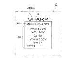
- FIG. 2B white and black are reversed in view of the visibility of the drawing. That is, the background is shown in white (ground color), and the nameplate information (character 46, symbol 47, specification character 48, two-dimensional code 49) as the mark part 41 (mark part 40) is shown in black.
- the information character 46, symbol 47, specification character 48, two-dimensional code 49
- the two-dimensional code includes a bar code and other plane codes. In particular, a barcode is preferable because of its high versatility and ease of laser processing.
- the characters 46 can display the manufacturer, product name, product number, etc.
- the symbols 47 can display warnings, special graphic characters, etc.
- the specification characters 48 can display specifications (information on electrical characteristics, etc.). It is not limited to.
- FIG. 2B only shows examples of display contents (information) of the nameplate, and the display contents are not limited to these.
- the resin sealing portion 30 uses black ionomer resin as the sealing resin. Therefore, since the solar cell module 1 forms the resin sealing portion 30 with a black ionomer resin, the solar cell module 1 improves the endothermic property with respect to the laser light in the resin sealing portion 30, so that the discoloration of the ionomer resin by the laser light is effective. Therefore, the mark unit 40 can display the information with high accuracy.
- the sealing resin (ionomer resin) applied for forming the resin sealing portion 30 preferably contains carbon black. That is, in the present embodiment, since the resin sealing portion 30 (sealing resin) contains carbon black, the mark portion that effectively displays the discoloration of the carbon black by the laser light and displays the information more clearly. 40, and the recognition rate is improved in both visual recognition and automatic recognition using a camera or the like.
- the mark portion 41 (mark portion 40) is formed as a nameplate, information as a nameplate is displayed. Therefore, since the mark part 41 (mark part 40) includes the mark part 41 that displays information (for example, a manufacturer) as a nameplate in a form that protects it from the outside, the nameplate information is displayed without attaching the nameplate. This improves product reliability and ease of handling.
- the mark part 41 (mark part 40) displays information on electrical characteristics. Therefore, since the solar cell module 1 can display information on electrical characteristics (electrical specifications) without attaching a nameplate, the reliability of the product and the ease of handling are improved.
- the mark part 41 (mark part 40) includes a display by a two-dimensional code. Therefore, since the solar cell module 1 can automatically read a code reader that reads a two-dimensional code, it is possible to efficiently deal with handling and maintenance.
- the resin sealing portion 30 contains carbon black, and the light beam (laser beam) discolors the carbon black to mark the mark portion. 41 displays information. Therefore, the manufacturing method of the solar cell module 1 forms the mark portion 41 by irradiating the light beam to change the color of the carbon black, so that the mark portion 41 having a high recognition rate can be formed.
- Embodiment 3 With reference to FIG. 3A and FIG. 3B, the solar cell module which concerns on this Embodiment, and the manufacturing method of a solar cell module are demonstrated. Since the basic configuration is the same as that of the first embodiment and the second embodiment, reference numerals are appropriately used and different items will be mainly described. In addition, about the manufacturing method of the solar cell module 1 which concerns on this Embodiment, Embodiment 7 demonstrates further detail.
- FIG. 3A is an enlarged cross-sectional view showing an essential part of the solar cell module 1 according to Embodiment 3 of the present invention.
- FIG. 3B is an enlarged plan view showing a display state of the nameplate formed on the mark portion 43 (mark portion 40) of the solar cell module 1 viewed in the direction of arrow B in FIG. 3A.
- the mark portion 43 (mark portion 40) is formed in the embedded member 42 embedded in the resin sealing portion 30. Therefore, the solar cell module 1 forms the mark portion 43 by the embedded member 42 embedded in the resin sealing portion 30 even when the temperature resistance of the sealing resin forming the resin sealing portion 30 is not sufficient. Productivity and reliability can be improved.
- the mark part 43 in the present embodiment is formed from the second translucent substrate 12 side.
- a name plate is formed by performing laser processing on the embedded member 42. That is, laser processing is performed by adjusting the focus of the laser light to the position of the embedded member 42.
- black colored PET polyethylene terephthalate
- copper foil or the like
- the heat generated by the laser processing is effectively generated by making the PET black, it is possible to easily and efficiently form the mark portion 40 with a high recognition rate.
- the embedded member 42 is embedded in the resin sealing portion 30 with respect to the state in which the first light transmitting substrate 11 and the solar cell portion 20 are formed, the element side insulating sheet 32, the embedded member 42, the covering insulating sheet 33,
- the two light-transmitting substrates 12 are sequentially laminated and heated and pressurized by a vacuum laminating apparatus (vacuum laminating step).
- the element side insulating sheet 32 and the covering insulating sheet 33 are integrated as the resin sealing portion 30 by heat and pressure in the vacuum laminating process.
- the two-layer configuration of the element side insulating sheet 32 and the covering insulating sheet 33 will be described in more detail in the seventh embodiment.
- the element-side insulating sheet 32 and the covering insulating sheet 33 are formed into a sheet shape with, for example, ionomer resin and are transparent.
- the covering insulating sheet 33 is thin (for example, it has been experimentally confirmed that 300 ⁇ m or less is preferable) in order to prevent discoloration due to laser processing.
- the thickness of the embedded member 42 is preferably set to, for example, 300 ⁇ m or less so that bubbles are not generated in the resin sealing portion 30 around the embedded member 42 in the vacuum laminating process using a vacuum laminating apparatus.
- the buried member 42 has a thickness of 50 ⁇ m, for example.
- the covering insulating sheet 33 is shown as being disposed corresponding to the entire surface of the solar cell module 1 (FIG. 3A), but covers the embedded member 42 so as to be slightly larger than the planar shape of the embedded member 42 (implementation). It is preferable to reduce the material.
- the display information (FIG. 3B) of the mark part 43 (mark part 40) is the same as in the second embodiment. Specifically, since the embedded member 42 is black, the display state is the same as that of the second embodiment within the range of the embedded member 42.
- Embodiment 4 With reference to FIG. 4A and FIG. 4B, the solar cell module which concerns on this Embodiment, and the manufacturing method of a solar cell module are demonstrated. Since the basic configuration is the same as that of the first to third embodiments, the reference numerals are appropriately used and different items are mainly described. In addition, about the manufacturing method of the solar cell module 1 which concerns on this Embodiment, Embodiment 8 demonstrates further detail.
- FIG. 4A is an enlarged cross-sectional view showing an essential part of the solar cell module 1 according to Embodiment 4 of the present invention.
- FIG. 4B is an enlarged plan view showing the display state of the nameplate formed on the mark portion 44 (mark portion 40) of the solar cell module 1 viewed in the direction of arrow B in FIG. 4A.
- the mark portion 44 (mark portion 40) is formed on the second light-transmissive substrate 12. Therefore, since the solar cell module 1 forms the mark part 44 (mark part 40) in the 2nd translucent board
- the resin sealing portion 30 is irrelevant to laser processing, it is formed of a transparent or black ionomer resin. However, as described above, in order to improve the visibility of the mark portion 44, black or other colors are used. It is preferable to have it. By setting the background to black, when the mark portion 44 is formed on the second translucent substrate 12, the mark portion 44 having a high recognition rate can be obtained.
- the mark part 44 is arranged on the outer surface 12s side from the center of the thickness of the second light-transmitting substrate 12. Therefore, since the solar cell module 1 arrange
- the information (display contents) indicated by the mark portion 44 (mark portion 40) as a nameplate in FIG. 4B is simplified with respect to the information of the mark portion 41 shown in FIG. 2B and the information of the mark portion 43 shown in FIG. 3B. Yes. Since the laser processing on the second light-transmissive substrate 12 made of a glass plate requires a long time, the display content of the mark portion 44 (name plate) is simplified. When the mark part 44 is simplified, the mark part 40 (mark part 41, mark part 43) shown in other embodiments can be used in combination. FIG. 4B only shows an example when the display content (information) of the nameplate is simplified, and the display content is not limited to these.
- the solar cell module 1 it is preferable to perform laser processing with a focal position outside the center of the thickness of the second light-transmissive substrate 12.
- the focal position is closer to the resin sealing portion 30 than the center of the thickness of the second translucent substrate 12, the influence on the resin sealing portion 30 and further, the solar cell portion 20 (back surface electrode, photoelectric conversion). This is because there is a risk that the solar cell unit 20 may be damaged.
- the position of the mark portion 44 in the thickness direction of the second light transmissive substrate 12 may be focused at a position having a depth of about 0.5 mm or more from the outer surface 12s of the second light transmissive substrate 12. preferable. This is to suppress the probability that the mark portion 44 is erased even when the outer surface 12 s of the second light-transmissive substrate 12 is scraped by an external mechanical influence. Therefore, when the thickness of the second translucent substrate 12 is about 4 mm, for example, the position of the mark portion 44 is preferably about 0.5 mm to 2 mm from the outer surface 12s.
- substrate 11 the solar cell part 20, the insulating sheet 31 (refer FIG. 5B. Resin sealing part 30), and the 2nd translucent board
- a part of the mark portion 40 is not affected by the result of characteristic inspection. It is also possible to form a symbol such as a manufacturer's logotype or CE mark.
- the solar cell module 1 according to the present embodiment is the same as the solar cell module 1 shown in the first to fourth embodiments.
- the manufacturing method of the solar cell module 1 which concerns on this Embodiment is the resin sealing part 30 with respect to the solar cell part 20 (solar cell element part 20c) simplified and shown in Embodiment 1 thru
- the present invention relates to a method for laminating the second light-transmissive substrate 12, a method for attaching the terminal box 50, and a method for forming the mark portion 40 (mark portion 41, mark portion 43, mark portion 44).
- the solar cell part 20 which concerns on this Embodiment is comprised with the thin film solar cell as shown in Embodiment 1.
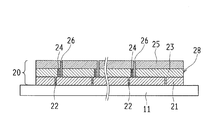
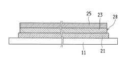
- FIG. 5A is an enlarged cross-sectional view showing an enlarged state of a main part in which solar cell unit 20 (thin film solar cell) is formed on first light-transmissive substrate 11 in solar cell module 1 according to Embodiment 5 of the present invention. It is.
- a transparent electrode layer 21, a photoelectric conversion layer 23, and a back electrode layer 25 are laminated in this order from the first light-transmissive substrate 11 side.
- the first separation groove 22 separates the transparent electrode layer 21 for each solar cell element part 20c
- the second separation groove 26 separates the photoelectric conversion layer 23 and the back electrode layer 25 for each solar cell element part 20c.
- the photoelectric conversion layer 23 is formed with a contact line 24 that connects the solar cell element portions 20c to each other, and the contact line 24 is formed on one transparent electrode layer 21 between the adjacent solar cell element portions 20c.
- the other back electrode layer 25 is connected.
- the solar cell element portion 20c is formed in a strip shape (see FIG. 5B) by the second separation groove 26, and the solar cell element portions 20c adjacent to each other are connected in series to constitute the solar cell module 1. That is, the solar cell module 1 which connects the solar cell element parts 20c in series and generates an output voltage corresponding to the number of series is configured.
- FIG. 5B is an exploded view showing the insulating sheet 31 forming the resin sealing portion 30 in the solar cell module 1 according to Embodiment 5 of the present invention and the second translucent substrate 12 laminated on the insulating sheet 31. It is a perspective view.
- a collector electrode 15p (positive collector electrode) is disposed on one of the solar cell element portions 20c disposed at both ends of the first light-transmissive substrate 11, and a collector electrode 15m (minus) is disposed on the other solar cell element portion 20c.
- Current collecting electrode The extraction lead 17 is connected to each of the collecting electrode 15p and the collecting electrode 15m.
- An insulating sheet 16 that insulates the extraction lead 17 from the solar cell element portion 20 c is disposed between the solar cell element portion 20 c and the extraction lead 17. The leading end of the extraction lead 17 is bent in a direction perpendicular to the solar cell unit 20 in order to lead the extraction lead 17 to the outside.
- the insulating sheet 31 that acts as a sealing resin for forming the resin sealing portion 30 is provided with an opening 31 h that leads the tip of the take-out lead 17 to the outside.
- a lead connection hole 12 h that leads the lead 17 to the outside is also formed in the second translucent substrate 12. Therefore, the leading end of the take-out lead 17 is led out to the outside through the opening 31h and the lead connection hole 12h (see FIG. 5C).
- the specific form of the insulating sheet 31 is different in each of the second to fourth embodiments.
- the insulating sheet 31 is, for example, a sealing resin (adhesive) obtained by molding a black ionomer resin into a sheet shape.
- the insulating sheet 31 is composed of two layers of the element side insulating sheet 32 and the covering insulating sheet 33, and is laminated with the black embedded member 42 interposed therebetween. That is, since the embedded member 42 is formed in black and the mark portion 41 is formed in the embedded member 42 by laser processing, the insulating sheet 31 (element-side insulating sheet 32, covering insulating sheet 33) is made of, for example, a transparent ionomer resin. Is done. Details of the element side insulating sheet 32 and the covering insulating sheet 33 will be further described in the seventh embodiment.
- the insulating sheet 31 is irrelevant to the laser processing, and may be either transparent or black as long as it is an ionomer resin, for example.
- FIG. 5C is a perspective view showing a state in which the resin-sealed portion 30 is formed by laminating the first light-transmissive substrate 11 and the second light-transmissive substrate 12 in the solar cell module 1 according to Embodiment 5 of the present invention. It is.
- the first light-transmitting substrate 11 and the second light-transmitting substrate 12 are laminated (adhered) with the solar cell portion 20 and the resin sealing portion 30 interposed therebetween.
- the leading end of the lead 17 is led out from the lead connection hole 12h.
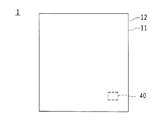
- FIG. 5D is a plan view showing an external appearance of the second translucent substrate 12 side after the terminal box 50 and the mark portion 40 are formed in the solar cell module 1 according to Embodiment 5 of the present invention.
- the module lead 51 is connected to the tip of the take-out lead 17, and the connection portion between the take-out lead 17 and the module lead 51 is connected to the second portion.
- the terminal box 50 mounted on the translucent substrate 12 is covered and protected.
- the module lead 51 is taken out from the terminal box 50 and applied to connection with other solar cell modules 1.
- the mark portion 40 is formed on the solar cell module 1.
- the specific configuration of the mark unit 40 is as shown in the second to fourth embodiments.
- or FIG. 17C the manufacturing method of the solar cell module which concerns on this Embodiment, and a solar cell module is demonstrated.
- the solar cell module and the solar cell module manufacturing method according to the present embodiment relate to a more specific structure and manufacturing method of the solar cell module 1 shown in the first to fifth embodiments (particularly the embodiment). 2, which corresponds to a detailed embodiment of FIG. 2A and FIG. 2B.) Therefore, reference numerals are appropriately used and different items will be mainly described.
- the solar cell part 20 of the solar cell module 1 according to the present embodiment is formed as a thin film solar cell and can be applied to other embodiments as it is. Moreover, below, it is set as the solar cell module 1 including the state before completion.
- FIG. 6A is a schematic plan view showing a schematic state of the solar cell module 1 according to Embodiment 6 of the present invention on the first translucent substrate 11 side.
- FIG. 6B is a schematic plan view showing a schematic state of the solar cell module 1 according to Embodiment 6 of the present invention on the second light transmissive substrate 12 side.
- the solar cell unit 20 of the solar cell module 1 is a thin film solar cell. Therefore, on the first light transmissive substrate 11 side, a state in which the strip-shaped solar cell element portions 20c are arranged in series via the first light transmissive substrate 11 is shown. In addition, the 1st separation groove 22 is arrange
- the resin sealing portion 30 is made of, for example, a black ionomer resin on the second translucent substrate 12 side, a black state is shown and the mark portion 40 can be visually recognized from the outside. Has been. Note that the mark portion 40 is formed in various states (see the mark portion 41, the mark portion 43, and the mark portion 44 in the first to fourth embodiments). .
- the first translucent substrate 11 and the second translucent substrate 12 are made of a glass plate having a width of 1000 mm ⁇ a length of 1400 mm ⁇ a thickness of about 4 mm. Insulation separation that isolates and isolates the solar cell element portion 20c from the periphery around the solar cell portion 20 (solar cell element portion 20c) (peripheral end portions of the first light-transmissive substrate 11 and the second light-transmissive substrate 12). Region 28 is formed.
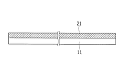
- FIG. 7A is a cross-sectional view showing a cross section when the transparent electrode layer 21 is laminated on the first translucent substrate 11 in the manufacturing process of the solar cell module 1 as viewed in the direction of arrows AA in FIG. 6A. Note that some hatchings in the cross section may be omitted in consideration of the visibility of the drawings (the same applies to the following embodiments).
- FIG. 7B is a cross-sectional view showing a cross section when the transparent electrode layer 21 is laminated on the first translucent substrate 11 in the manufacturing process of the solar cell module 1 seen in the direction of arrow BB in FIG. 6A.
- the transparent electrode layer 21 is formed by laminating SnO 2 by thermal CVD (vapor phase growth method) on the surface of the first translucent substrate 11 on the side where the solar cell unit 20 is formed.
- FIG. 8A is a cross-sectional view showing a cross section when the transparent electrode layer 21 is separated by the first separation groove 22 in the manufacturing process of the solar cell module 1 seen in the direction of arrow AA in FIG. 6A.
- FIG. 8B is a cross-sectional view showing a cross section when the transparent electrode layer 21 is separated by the first separation groove 22 in the manufacturing process of the solar cell module 1 as seen in the direction of arrow BB in FIG. 6A.
- first light-transmissive substrate 11 First formed in the longitudinal direction of the solar cell element portion 20c (hereinafter referred to as “longitudinal direction of the first light-transmissive substrate 11”) by irradiation with a fundamental wave (wavelength 1064 nm) of a YAG (Yttrium Aluminum Garnet) laser beam.
- the transparent electrode layer 21 is separated by the separation groove 22. That is, a region corresponding to the solar cell element portion 20 c is defined by the first separation groove 22 formed in the transparent electrode layer 21.
- the fundamental wave of the YAG laser beam is irradiated.
- the part of the transparent electrode layer 21 is removed, and a strip-shaped first separation groove 22 for separating the transparent electrode layer 21 into a strip shape is formed.
- a fundamental wave of YVO 4 (Yttrium Orthovanadate) laser light (wavelength 1064 nm) or a fundamental wave of fiber laser light (wavelength 1064 nm) may be used.
- the first translucent substrate 11 on which the first separation grooves 22 were formed was ultrasonically cleaned with pure water.
- FIG. 9A is a cross-sectional view showing a cross section when the photoelectric conversion layer 23 is formed in the manufacturing process of the solar cell module 1 as viewed in the direction of arrows AA in FIG. 6A.
- FIG. 9B is a cross-sectional view showing a cross section when the photoelectric conversion layer 23 is formed in the manufacturing process of the solar cell module 1 as seen in the direction of arrow BB in FIG. 6A.
- a photoelectric conversion layer 23 was formed so as to cover the transparent electrode layer 21 in which the first separation groove 22 was formed.
- the photoelectric conversion layer 23 includes a p layer made of a p-type hydrogenated amorphous silicon film, an i layer made of an i-type hydrogenated amorphous silicon film, and an n layer made of an n-type hydrogenated amorphous silicon film in this order.
- a top cell an amorphous silicon film power generation element having a pin structure
- a bottom cell (a microcrystalline silicon film power generation element having a pin structure) is formed by stacking an i layer made of n and an n layer made of an n-type microcrystalline silicon film in this order.
- a semiconductor photoelectric conversion layer can be used as the photoelectric conversion layer 23.
- a p-layer, an i-layer, and an n-layer made of an amorphous silicon thin film are stacked in this order from the first translucent substrate 11 side.
- a cell (first photoelectric conversion layer) and a bottom cell (second photoelectric conversion layer) in which a p layer, an i layer, and an n layer made of a microcrystalline silicon thin film are stacked in this order on the top cell are stacked. can do.
- the amorphous silicon thin film (first photoelectric conversion layer) and the microcrystalline silicon thin film (second photoelectric conversion layer) can be formed by, for example, a plasma CVD method.
- a top cell in which a p layer, an i layer, and an n layer made of an amorphous silicon thin film are stacked in this order from the first light transmitting substrate 11 side.
- a middle cell in which a p layer, an i layer, and an n layer made of an amorphous silicon thin film are laminated in this order on the top cell, and a p layer made of a microcrystalline silicon thin film on the middle cell , I layer, and n layer can be stacked to form a bottom cell (third photoelectric conversion layer).
- the amorphous silicon thin film (first photoelectric conversion layer, second photoelectric conversion layer) and microcrystalline silicon thin film (third photoelectric conversion layer) can be formed by, for example, a plasma CVD method.
- a photoelectric conversion layer exceeding three layers can be formed.
- Each photoelectric conversion layer from the first photoelectric conversion layer to the third photoelectric conversion layer is formed of a silicon-based semiconductor of the same type (for example, an i layer for an amorphous silicon thin film as a p layer and an amorphous silicon thin film as an n layer).
- they may be formed of different types of silicon-based semiconductors (for example, an i layer for an amorphous silicon thin film as a p layer and a microcrystalline silicon thin film as an n layer).
- the p-type semiconductor layer and the i-type semiconductor layer may be formed using amorphous silicon
- the n-type semiconductor layer may be formed using microcrystalline silicon.
- the p-type semiconductor layer and the n-type semiconductor layer may be formed of silicon carbide or silicon germanium, and the i-type semiconductor layer may be formed of silicon.
- the p-type, i-type, and n-type semiconductor layers may have a single-layer structure or a multi-layer structure. Each layer in the case of a multi-layer structure may be formed of different types of silicon-based semiconductors.
- amorphous silicon thin film includes a thin film made of a hydrogenated amorphous silicon-based semiconductor (a-Si: H) in which dangling bonds of silicon are terminated with hydrogen.
- a-Si: H hydrogenated amorphous silicon-based semiconductor
- microcrystalline silicon thin film includes a thin film made of a hydrogenated microcrystalline silicon-based semiconductor ( ⁇ c-Si: H) in which dangling bonds of silicon are terminated with hydrogen.
- the thickness of the photoelectric conversion layer 23 is not particularly limited, and can be, for example, 200 nm or more and 5 ⁇ m or less. Moreover, the formation method of the photoelectric converting layer 23 is not limited to the plasma CVD method.
- FIG. 10A is a cross-sectional view showing a cross section when the contact line 24 is formed in the manufacturing process of the solar cell module 1 as viewed in the direction of arrow AA in FIG. 6A.
- FIG. 10B is a cross-sectional view showing a cross section when the contact line 24 is formed in the manufacturing process of the solar cell module 1 as seen in the direction of arrow BB in FIG. 6A.
- the photoelectric conversion layer 23 By irradiating the photoelectric conversion layer 23 from the first translucent substrate 11 side while moving the second harmonic (wavelength 532 nm) of the YAG laser light in the longitudinal direction of the first translucent substrate 11, the photoelectric conversion layer A strip-shaped contact line 24 for separating 23 into strips was formed.
- a second harmonic (wavelength: 532 nm) of YVO 4 laser light may be used as the light beam for forming the contact line 24.
- FIG. 11A is a cross-sectional view showing a cross section when the back electrode layer 25 is formed in the manufacturing process of the solar cell module 1 as viewed in the direction of arrows AA in FIG. 6A.
- FIG. 11B is a cross-sectional view showing a cross section when the back electrode layer 25 is formed in the manufacturing process of the solar cell module 1 as seen in the direction of arrow BB in FIG. 6A.
- a back electrode layer 25 was formed so as to cover the photoelectric conversion layer 23 on which the contact line 24 was formed.
- the back electrode layer 25 was formed by forming a 50 nm thick ZnO (zinc oxide) film by magnetron sputtering and then laminating a 125 nm thick Ag (silver) film.
- FIG. 12A is a cross-sectional view showing a cross section when the second separation groove 26 is formed in the manufacturing process of the solar cell module 1 seen in the direction of arrow AA in FIG. 6A.
- FIG. 12B is a cross-sectional view showing a cross section when the second separation groove 26 is formed in the manufacturing process of the solar cell module 1 as seen in the direction of arrow BB in FIG. 6A.
- a strip-shaped second separation groove 26 for separating the layer 23 and the back electrode layer 25 into a strip shape was formed.
- the second harmonic of the YVO 4 laser beam may be used as the light beam that forms the second separation groove 26.
- a plurality of solar cell element portions 20c are formed in a direction orthogonal to the longitudinal direction of the first translucent substrate 11 (left and right direction in the drawing of FIG. 12A). 20c will be in the state connected in series with respect to the other adjacent solar cell element part 20c. That is, the solar cell unit 20 (solar cell string) was formed by the plurality of solar cell element units 20c electrically connected in series.
- FIG. 13A is a cross-sectional view showing a cross section when the peripheral groove 27 is formed in the manufacturing process of the solar cell module 1 as seen in the direction of arrow AA in FIG. 6A.
- FIG. 13B is a cross-sectional view showing a cross section when the peripheral groove 27 is formed in the manufacturing process of the solar cell module 1 seen in the direction of arrow BB in FIG. 6A.
- the peripheral groove 27 was formed in the direction orthogonal to the longitudinal direction of the first translucent substrate 11 by irradiating the second harmonic of the YAG laser beam.
- the peripheral groove 27 is formed by removing the back electrode layer 25 and the photoelectric conversion layer 23.
- 14A is a cross-sectional view showing a cross section when the insulating isolation region 28 is formed in the manufacturing process of the solar cell module 1 as seen in the direction of arrow AA in FIG. 6A.
- FIG. 14B is a cross-sectional view showing a cross section when the insulating isolation region 28 is formed in the manufacturing process of the solar cell module 1 as seen in the direction of arrow BB in FIG. 6A.
- Irradiation is performed while moving the fundamental wave of the YAG laser beam so as to surround the periphery of the solar cell string (the solar cell unit 20 formed by connecting the solar cell element units 20c in series) (laser beam irradiation width: 650 ⁇ m).
- the transparent electrode layer 21, the photoelectric conversion layer 23, and the back electrode layer 25 were removed to form the insulating isolation region 28.
- the insulating isolation region 28 is formed by removing the transparent electrode layer 21, the photoelectric conversion layer 23, and the back electrode layer 25 from the end of the first translucent substrate 11 by about 12 mm in width.
- a fundamental wave of YVO 4 laser light may be used as a light beam for forming the insulating isolation region 28.
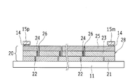
- FIG. 15A is a cross-sectional view showing a cross section when the collecting electrode 15p and the collecting electrode 15m are formed in the manufacturing process of the solar cell module 1 as seen in the direction of arrow AA in FIG. 6A.
- FIG. 15B is a cross-sectional view showing a cross section when the collecting electrode 15p and the collecting electrode 15m are formed in the manufacturing process of the solar cell module 1 seen in the direction of arrow BB in FIG. 6A.
- a collector electrode 15p was formed on one side of the solar cell element portion 20c located at both ends of the solar cell string (solar cell portion 20), and a collector electrode 15m was formed on the other side.
- the collecting electrode 15p and the collecting electrode 15m are connected to the back electrode layer 25 of the solar cell element portion 20c through a metal paste 14 made of silver paste. Further, the current collecting electrode 15p and the current collecting electrode 15m are arranged extending in the longitudinal direction of the solar cell element portion 20c (see FIG. 5B).
- 16A is a cross-sectional view showing a cross section when the resin sealing portion 30 and the second light-transmitting substrate 12 are laminated and bonded in the manufacturing process of the solar cell module 1 as seen in the direction of arrows AA in FIG. 6A. It is.
- 16B is a cross-sectional view showing a cross section when the resin sealing portion 30 and the second light-transmitting substrate 12 are laminated and bonded in the manufacturing process of the solar cell module 1 seen in the direction of arrow BB in FIG. 6A. It is.
- substrate 12 are piled up, the solar cell part 20 is resin-sealed, and the solar cell module 1 is attached. Form.
- An insulating sheet 31 (see FIG. 5B) as a sealing resin molded into a sheet shape by adding black carbon to an ionomer resin in which the molecules of the ethylene methacrylic acid copolymer are cross-linked with metal ions is formed into a sheet shape.
- a tempered back glass (second translucent substrate 12) having a thickness of 3.2 mm is overlaid on the insulating sheet 31, and then the solar cell unit 20 is placed by a vacuum laminating apparatus (vacuum laminating step).
- the resin sealing portion 30 and the second translucent substrate 12 were laminated and bonded.
- FIG. 17A is a cross-sectional view showing a cross section when the mark portion 41 (mark portion 40) is formed in the manufacturing process of the solar cell module 1 seen in the direction of arrow AA in FIG. 6A.
- FIG. 17B is a cross-sectional view showing a cross section when the mark portion 41 (mark portion 40) is formed in the manufacturing process of the solar cell module 1 seen in the direction of arrow BB in FIG. 6A.
- FIG. 17C is a plan view showing a state of bubbles generated when the formation condition of the mark portion 41 (mark portion 40) is changed in FIG. 17A.
- the terminal box 50 (see FIG. 5D) is mounted on the second light-transmissive substrate 12 of the solar cell module 1, the terminal box is filled with silicone resin (not shown), and a final output inspection is performed. In addition, you may implement an output test
- the laser sealing process is performed on the resin sealing portion 30 from the second translucent substrate 12 side to form the mark portion 41.
- the position of the mark portion 41 in the thickness direction is preferably such that the laser beam is focused on the side close to the second light transmissive substrate 12. This is because the solar cell unit 20 is not affected by the heat of the laser beam.
- the mark portion 41 is formed as a nameplate.
- the display mode of the nameplate is, for example, as shown in FIG. 2B of the second embodiment.
- a second harmonic (wavelength: 532 nm) of a YVO 4 laser was used as a laser beam to be used.
- a second harmonic (wavelength 532 nm) of a YAG laser may be used. That is, a SHG (Second Harmonic Generation) laser can be applied.
- the SHG laser is a second harmonic that generates a second harmonic wavelength (second harmonic (wavelength 532 nm) with respect to 1064 nm) with respect to a fundamental wavelength (for example, the fundamental wavelength 1064 nm of a YVO 4 laser). It is a generation laser.
- the present inventor When the present inventor performs processing with a laser beam in the same infrared region as the fundamental wave (wavelength 1064 nm) of each laser, the amount of gas generated in the resin sealing portion 30 increases due to the influence of heat from the laser beam. In addition, it has been newly found that gas accumulation tends to occur in the laser processed region.
- the gas reservoir is visually recognized as bubbles 41b (FIG. 17C) from the outside, and there is a risk of causing poor appearance and reduced visibility (recognition rate reduction).
- processing can also be performed with the third harmonic (wavelength 355 nm) of a YVO 4 laser.
- the processing conditions for forming the mark portion 41 were a processing point power of 1.5 W, a repetition frequency of 30 KHz, and a processing speed of 1000 mm / s.
- the energy density (J / mm 2 ) at the processing point is preferably between 0.015 (J / mm 2 ) and 0.07 (J / mm 2 ). If it is less than 0.015 (J / mm 2 ), the processing margin is reduced, the discoloration (color development) is poor, and the character recognition is poor. On the other hand, if it exceeds 0.07 (J / mm 2 ), bubbles are likely to be generated.
- the processing conditions at this time are conditions when a second harmonic (532 nm) laser beam is applied to the black ionomer resin.
- a galvano scanner system is advantageous in terms of tact.
- the light beam is preferably generated by an SHG laser. That is, in the method for manufacturing solar cell module 1 according to the present embodiment, the light beam is generated by the SHG laser, so it is possible to suppress the generation of heat and prevent the generation of bubbles, and improve the quality and the recognition rate. be able to.
- FIG. 18A and FIG. 18B With reference to FIG. 18A and FIG. 18B, the solar cell module which concerns on this Embodiment, and the manufacturing method of a solar cell module are demonstrated.
- the solar cell module and the manufacturing method of the solar cell module according to the present embodiment relate to a more specific structure and manufacturing method of the solar cell module 1 shown in the first to sixth embodiments (particularly the embodiment). 3, corresponding to the detailed embodiment for FIG. 3A and FIG. 3B).
- the solar cell unit 20 of the solar cell module 1 according to the present embodiment is formed as a thin film solar cell.
- the solar cell module 1 including a state before completion is used.
- FIG. 18A is a cross-sectional view showing a cross section when the mark portion 43 (mark portion 40) is formed in the manufacturing process of the solar cell module 1 as seen in the direction of arrow AA in FIG. 6A.
- FIG. 18B is a cross-sectional view showing a cross section when the mark portion 43 (mark portion 40) is formed in the manufacturing process of the solar cell module 1 seen in the direction of arrow BB in FIG. 6A.
- the mark portion 41 (mark portion 40) is not directly formed by laser processing on the resin sealing portion 30 (the second and sixth embodiments), but the resin sealing portion 30 (element side).
- the embedded member 42 was embedded in the insulating sheet 32 and the covering insulating sheet 33), and the embedded member 42 was subjected to laser processing to form the mark portion 43 (mark portion 40).
- the embedded member 42 is 100 mm square and 50 ⁇ m thick black PET (see Embodiment 3). By making the embedded member 42 black, the visibility of the mark portion 43 can be improved and a high recognition rate can be realized.
- the embedded member 42 is disposed on the element-side insulating sheet 32, the covering insulating sheet 33 is disposed so as to cover the embedded member 42, and the solar cell module 1 is vacuum-laminated with the second light-transmitting substrate 12 overlaid thereon.
- a heat and pressure treatment is performed by an apparatus (vacuum laminating step).
- the embedding member 42 is embedded in the resin sealing portion 30 (the element side insulating sheet 32 and the covering insulating sheet 33) by the vacuum laminating process.
- the element side insulating sheet 32 and the covering insulating sheet 33 are integrated in a vacuum laminating process to constitute the resin sealing portion 30.
- the covering insulating sheet 33 has a larger planar shape than the embedded member 42 in order to completely cover the embedded member 42, and specifically, is 125 mm square.
- the covering insulating sheet 33 was formed by molding an ionomer resin in which the molecules of the ethylene methacrylic acid copolymer were cross-linked with metal ions into a transparent sheet shape to a thickness of 100 ⁇ m.
- the second harmonic (532 nm) of the YVO 4 laser was used as the laser beam, and the processing conditions when forming the mark portion 43 were a processing point power of 0.4 W, a repetition frequency of 30 KHz, and a processing speed of 1000 mm / s.
- the burying member 42 is separated from the second light-transmitting substrate 12 because it does not have adhesiveness to the second light-transmitting substrate 12 (glass plate). Maintain state. Therefore, the appearance is not clear, and the gas (bubbles) generated when laser processing is performed further deteriorates the visibility. Therefore, it is preferable to use the covering insulating sheet 33 that covers the embedded member 42.
- the thickness of the embedded member 42 is preferably 300 ⁇ m or less. This is because if it exceeds 300 ⁇ m, bubbles are generated around the embedded member 42 in the vacuum laminating process. In addition, if the thickness of the covering insulating sheet 33 exceeds 300 ⁇ m, the transparent covering insulating sheet 33 may be slightly discolored by the laser beam, and therefore it is preferably 300 ⁇ m or less.
- the covering insulating sheet 33 it is preferable to select a material having less absorption with respect to the wavelength band of the laser light to be used.
- the covering insulating sheet 33 according to the present embodiment has a slightly larger size than the embedded member 42. Although it is possible to cover the entire first transparent substrate 11, the second transparent substrate 12, and the resin sealing portion 30 (insulating sheet 31) (1000 mm ⁇ 1400 mm), the material cost is considered. Then, it is more preferable to arrange partially.
- copper foil or the like is applicable in addition to PET. That is, any material that can be marked by laser processing may be used.
- the mark part 43 is formed as a nameplate.
- the display form of the nameplate is, for example, as shown in FIG. 3B of the third embodiment.
- FIG. 19A and FIG. 19B With reference to FIG. 19A and FIG. 19B, the solar cell module which concerns on this Embodiment, and the manufacturing method of a solar cell module are demonstrated.
- the solar cell module and the solar cell module manufacturing method according to the present embodiment relate to a more specific structure and manufacturing method of the solar cell module 1 shown in the first to seventh embodiments (particularly the embodiment). 4, corresponding to the detailed embodiment of FIG. 4A and FIG. 4B.) Therefore, the reference numerals are appropriately used and different items will be mainly described.
- the solar cell unit 20 of the solar cell module 1 according to the present embodiment is formed as a thin film solar cell.
- the solar cell module 1 including a state before completion is used.
- FIG. 19A is a cross-sectional view showing a cross section when the mark portion 44 (mark portion 40) is formed in the manufacturing process of the solar cell module 1 seen in the direction of arrow AA in FIG. 6A.
- FIG. 19B is a cross-sectional view showing a cross section when the mark portion 44 (mark portion 40) is formed in the manufacturing process of the solar cell module 1 seen in the direction of arrow BB in FIG. 6A.
- the mark portion 41 (mark portion 40) is not directly formed by laser processing on the resin sealing portion 30 (Embodiment 2 and Embodiment 6), but the second portion formed of a glass plate.
- the mark part 44 (mark part 40) was formed by performing laser processing inside the translucent substrate 12. Since it is a laser processing to a glass plate, it will be in the state which can be visually recognized as a cloudy state.
- mark part 40 mark part 44
- the visibility of the mark part 44 is improved. And a high recognition rate can be realized.
- the second harmonic (532 nm) of the YVO 4 laser was used as the laser beam, and the processing conditions when forming the mark portion 43 were a processing point power of 2.5 W, a repetition frequency of 20 KHz, and a processing speed of 250 mm / s.
- the focus position which performs laser processing adjusts a focus position to the outer side from the center (center surface 12c) of the thickness of a glass plate, ie, the side away from the resin sealing part 30.
- FIG. The reason is that the energy density at the processing point in this embodiment is as high as 0.410 (J / mm 2 ), and therefore the resin sealing portion 30 is also heated when the focal position is on the resin sealing portion 30 side. It is because there is a possibility of affecting.
- the resin sealing part 30 is transparent, there exists a possibility that a laser beam may permeate
- the processing time required for direct laser processing on a glass plate is longer than in other embodiments. Therefore, it is preferable to make the mark portion 44 as simple and compact as possible.
- the mark portion 44 For example, only the company name, model number, and two-dimensional code are laser processed as the mark portion 44, and other information (character information, specification character information, etc.)
- the mark part 41 may be combined with the form of the mark part 40 in other embodiments, such as forming the mark part 41 by laser processing on the resin sealing part 30.
- laser processing for the mark portion 40 in another embodiment is used in combination, it is preferable from the viewpoint of equipment cost or the like that laser processing with the same wavelength is performed so that the processing can be changed.
- the mark part 44 was formed as a nameplate.
- the display form of the nameplate is, for example, as shown in FIG. 4B of the fourth embodiment.
- the solar cell module according to the present embodiment and the method for manufacturing the solar cell module include a laser beam control method (laser) in laser processing applied to the solar cell module 1 shown in the first to eighth embodiments. Since the method relates to a light scanning method), reference will be made appropriately to the description, and different items will be mainly described. In the following description, the “character 46” is mainly described as an example, but the present invention can be similarly applied to a “graphic”.
- laser laser
- 20A to 20D are schematic diagrams for explaining the state of the laser beam processing unit 60 formed in the mark unit 40 of the solar cell module 1 according to Embodiment 9 of the present invention.
- FIG. 20A is a schematic diagram showing a laser beam processing unit 60 for the letter A formed on the mark unit 40 of the solar cell module 1 according to Embodiment 9 of the present invention.
- FIG. 20B is a schematic diagram showing a laser beam processing unit 60 for the letter B formed on the mark unit 40 of the solar cell module 1 according to Embodiment 9 of the present invention.
- FIG. 20C is a schematic diagram showing the laser beam processing unit 60 for the letter C formed on the mark unit 40 of the solar cell module 1 according to Embodiment 9 of the present invention.
- FIG. 20D is a schematic diagram showing a laser beam processing unit 60 for the letter T formed on the mark unit 40 of the solar cell module 1 according to Embodiment 9 of the present invention.
- a state where the laser processing is performed on the character 46 is shown as a laser beam processing unit 60.
- “A”, “B”, “T”, etc. as the character 46 have a portion (intersection 60 c) that intersects each other in the line representing the character, but “C”, etc., as the character 46, for example, There is no portion (intersection 60c) that intersects each other in the line representing the character.
- the laser light intersects at the intersecting portion 60c in the same manner as the original character line.
- the inventor of the present application newly found out that the influence of the heat of the laser light is increased at the intersection 60c, and for example, there is a possibility of generating bubbles.
- the laser beam scanning control is performed so that the laser beam does not intersect at the intersection 60c. That is, intersection avoidance scanning is performed on the laser beam so that the laser beam processing unit 60 does not intersect at the intersection 60c.
- the irradiation (laser processing) of the laser beam may be stopped for the portion (region) of the intersecting portion 60c included in the character 46.
- the typeface of the character 46 formed on the mark portion 40 is configured such that the intersecting portion 60c is omitted. Therefore, even when the mark unit 40 is formed by laser processing, the solar cell module 1 suppresses heat generation due to laser processing as compared with the case where laser processing is performed on the intersection 60c. The generation of bubbles can be prevented, and the visibility can be improved and the mark portion 40 having a high recognition rate can be realized. That is, it is preferable to suppress the influence of heat by laser processing (intersection avoidance processing) in which the laser beam is not irradiated to the intersection 60c.
- the character 46 is processed by scanning the laser beam adjacently in parallel several times.
- the thick character 46 can be formed.
- 20A to 20D show the case where the character 46 (A, B, C, T) is processed by three scanning lines, but the scanning line in the case of widening is three scanning lines. However, the number of scanning lines can be applied as necessary.
- the first scanning line 61, the second scanning line 62, and the third scanning line 63 simply indicate that laser processing is performed by a plurality of scanning lines, and is for distinguishing the plurality of scanning lines from each other. It is only description of.
- the influence of the heat of the laser beam is also suppressed by processing the character 46 having the intersection portion 60c by suppressing the machining point power, which is the processing condition of the laser beam, at the intersection portion 60c instead of the intersection avoidance processing. It is possible to obtain the same effect as when the intersection 60c is not formed.
- FIGS. 21A to 21C are schematic diagrams for explaining the state of the laser beam processing unit 60 formed in the mark unit 40 of the solar cell module 1 according to Embodiment 9 of the present invention.
- FIG. 21A is a schematic diagram showing a laser beam processing unit 60 when a wide character H formed on the mark unit 40 of the solar cell module 1 according to Embodiment 9 of the present invention is processed by the reciprocating scanning line 64. .
- FIG. 21B is a schematic diagram showing a laser beam processing unit 60 when a wide character H formed on the mark unit 40 of the solar cell module 1 according to Embodiment 9 of the present invention is processed by the parallel scanning lines 65. .
- FIG. 21C is a schematic diagram showing the laser beam processing unit 60 when processing is performed by omitting the character outline 46f of the wide character A formed in the mark unit 40 of the solar cell module 1 according to Embodiment 9 of the present invention. It is.
- the direction of the arrow superimposed on the line is the laser beam scanning direction (processing direction).
- logotypes, characters, symbols, etc. that include a large area that is about twice as large, it may be necessary to fill the inside of the contour.
- the inventor of the present application does not perform the folding process (reciprocal continuous process) by continuous scanning as shown by the reciprocating scanning line 64 (FIG. 21A), but the starting point (starting point region) and the end point of the scanning line. It is newly found that it is less susceptible to the influence of heat from the laser beam when the parallel scanning line 65 (FIG. 21B) that repeats scanning in parallel in the same direction by dividing the (end point region) regionally. I found out.
- the parallel scanning line 65 arrange
- the parallel scanning does not necessarily have to be parallel, and the scanning direction may be appropriately inclined so that the start points are separated but the end points coincide.
- wide characters are illustrated, but the present invention can be similarly applied to patterns such as figures.
- the start point position and the end point position are separated in the length direction of the wide area of the object to be processed. It is preferable to perform laser processing by scanning the laser beam in parallel from the start point side to the end point side.
- the inventor of the present application does not perform laser processing on the character outline 46f that is the peripheral part of the wide character (schematically shown by a broken line in FIG. 21C), and only on the inside of the character outline 46f. It was newly discovered that laser processing is less susceptible to the effects of heat from laser light. For convenience of explanation, wide characters are illustrated, but the present invention can be similarly applied to patterns such as figures.
- the filling process for the object to be processed (for example, the material before becoming the mark portion 40) by the laser beam according to the present embodiment is a laser process for irradiating the inner region excluding the outline of the painted region with the laser beam. It is preferable to apply. With this configuration, generation of bubbles in the resin sealing portion 30 can be prevented, and the visibility can be improved and the mark portion 40 with a high recognition rate can be realized.
- 22A to 22C are schematic diagrams for explaining the state of the laser beam processing unit 60 formed in the mark unit 40 of the solar cell module 1 according to Embodiment 9 of the present invention.
- FIG. 22A shows the first scanning line 61 and the second scanning line when laser processing is performed by scanning a plurality of laser beams in parallel when forming the mark portion 40 of the solar cell module 1 according to Embodiment 9 of the present invention. It is a schematic diagram which shows typically the relationship with the scanning line 62. FIG.
- FIG. 22B shows a case where the mark portion 40 of the solar cell module 1 according to Embodiment 9 of the present invention is formed, and the first scanning line 61 to the third scanning line 63 of the laser light are brought into close contact with each other to form the letter T.
- FIG. 22C shows a case where the mark portion 40 of the solar cell module 1 according to Embodiment 9 of the present invention is formed, and the first scanning line 61 to the third scanning line 63 of the laser light are separated from each other to form the letter T. It is a schematic diagram which shows typically the laser beam process part 60 when carrying out laser processing.
- the laser beam processing unit 60 is formed corresponding to the beam width Wb of the laser beam.
- parallel lines such as the first scanning line 61 and the second scanning line 62 can be processed (marked).
- the pitch (scanning interval) between the first scanning line 61 and the second scanning line 62, that is, the beam pitch Wp of the laser light can be adjusted as appropriate by controlling the laser processing apparatus.
- the inter-beam gap Ws of the laser light is defined according to the beam width Wb and the beam pitch Wp. Therefore, the laser processing state (for example, the marking state) differs by adjusting the beam pitch Wp.
- the inventor of the present application newly found out that the inter-beam gap Ws greatly affects the visibility during various studies on the visibility (recognition rate) of the marking in laser processing. That is, rather than increasing the beam pitch Wp to widen the inter-beam gap Ws, it is better to make the beam pitch Wp smaller and scan the laser beam so that there is no inter-beam gap Ws. I found out.
- the first scanning line 61 to the third scanning are performed by laser processing so that the first scanning line 61 to the third scanning line 63 are in contact with each other and overlap each other (FIG. 22B). Visibility can be improved as compared with the case where the lines 63 are separated from each other and laser processing is performed (FIG. 22C).
- the boundaries of the laser beam processing unit 60 with the laser beam are mutually aligned. It is preferable to overlap.
- the scanning line of the laser beam to be scanned later is brought into contact with the scanning line of the laser beam scanned earlier (the formed laser beam processing unit 60) so that no gap (gap between beams Ws) is generated. It is preferable to scan with a laser beam.
- the beam interval between the scanning lines is reduced. It is preferable to process the gap Ws so that there is no other material (for example, the sealing resin of the resin sealing portion 30 when the mark portion 41 is formed).
- the laser beams for example, the first scanning line 61 and the second scanning line 62
- the laser beams for example, the first scanning line 61 and the second scanning line 62
- the laser scanning method in laser processing according to the present embodiment can be applied as appropriate to the other embodiments.
- the embodiments can be applied to each other as long as they do not contradict each other.
- the solar cell module according to the present invention includes a mark portion formed between the boundary between the solar cell portion and the resin sealing portion and the outer surface of the second light transmissive substrate, the power generation region (power generation amount) It is possible to prevent the influence on the mark part and the influence on the mark part from the outside, and improve the mechanical strength of the mark part in the state of preventing the reduction of the power generation amount, and improve the durability, weather resistance and reliability. Useful in terms.
- the manufacturing method of the solar cell module which concerns on this invention is from the boundary of a solar cell part and a resin sealing part to the outer surface of a 2nd translucent board
Landscapes
- Photovoltaic Devices (AREA)
Abstract
Le module de cellule solaire (1) de la présente invention comprend, à partir du côté d'incidence de lumière solaire, un premier substrat transparent (11), une unité de cellule solaire (20), une partie d'étanchéité de résine (30), et un second substrat transparent (12) agencés (laminés) dans cet ordre. Ce module de cellule solaire (1) comporte une partie de repère (40) (formée dans une sous-région à l'intérieur de la région de formation de partie de repère (40r)) formée entre l'interface (30b) de l'unité de cellule solaire (20) et la partie d'étanchéité de résine (30) vers la surface externe (12s) du second substrat transparent (12).
Applications Claiming Priority (2)
| Application Number | Priority Date | Filing Date | Title |
|---|---|---|---|
| JP2011-044258 | 2011-03-01 | ||
| JP2011044258A JP2012182317A (ja) | 2011-03-01 | 2011-03-01 | 太陽電池モジュール、および太陽電池モジュールの製造方法 |
Publications (1)
| Publication Number | Publication Date |
|---|---|
| WO2012117775A1 true WO2012117775A1 (fr) | 2012-09-07 |
Family
ID=46757717
Family Applications (1)
| Application Number | Title | Priority Date | Filing Date |
|---|---|---|---|
| PCT/JP2012/051616 Ceased WO2012117775A1 (fr) | 2011-03-01 | 2012-01-26 | Module de cellule solaire et procédé de fabrication de module de cellule solaire |
Country Status (2)
| Country | Link |
|---|---|
| JP (1) | JP2012182317A (fr) |
| WO (1) | WO2012117775A1 (fr) |
Cited By (2)
| Publication number | Priority date | Publication date | Assignee | Title |
|---|---|---|---|---|
| WO2021260021A1 (fr) * | 2020-06-24 | 2021-12-30 | Sono Motors Gmbh | Procédé de fabrication d'un module photovoltaïque comprenant la découpe au laser d'une étiquette photovoltaïque |
| CN117733358A (zh) * | 2024-01-04 | 2024-03-22 | 江苏富乐华半导体科技股份有限公司 | 一种覆铜板雕刻二维码的返工方法 |
Families Citing this family (4)
| Publication number | Priority date | Publication date | Assignee | Title |
|---|---|---|---|---|
| JP2014075430A (ja) * | 2012-10-03 | 2014-04-24 | Sharp Corp | 太陽電池モジュール |
| KR101921237B1 (ko) * | 2013-01-16 | 2018-11-22 | 엘지전자 주식회사 | 건물 일체형 태양 전지 모듈 |
| JP6211783B2 (ja) * | 2013-03-29 | 2017-10-11 | 三井化学東セロ株式会社 | 太陽電池モジュール |
| EP4642196A1 (fr) * | 2022-12-21 | 2025-10-29 | Panasonic Holdings Corporation | Module de cellule solaire |
Citations (11)
| Publication number | Priority date | Publication date | Assignee | Title |
|---|---|---|---|---|
| JPS62176151A (ja) * | 1986-01-30 | 1987-08-01 | Toshiba Chem Corp | 樹脂封止型半導体装置 |
| JPS63213977A (ja) * | 1987-03-03 | 1988-09-06 | Matsushita Electric Ind Co Ltd | アモルフアス太陽電池 |
| JPH0451156U (fr) * | 1990-08-31 | 1992-04-30 | ||
| JP2001168357A (ja) * | 1999-12-08 | 2001-06-22 | Sharp Corp | 薄膜太陽電池モジュール及びその製造方法 |
| JP2001326373A (ja) * | 2000-05-15 | 2001-11-22 | Sharp Corp | 太陽電池モジュール |
| JP2002319694A (ja) * | 2001-04-20 | 2002-10-31 | Sharp Corp | 採光型合わせガラス構造太陽電池モジュール及び採光型複層構造太陽電池モジュール |
| JP2004503112A (ja) * | 2000-07-06 | 2004-01-29 | ビーピー・コーポレーション・ノース・アメリカ・インコーポレーテッド | 部分透過性光起電モジュール |
| JP2004152829A (ja) * | 2002-10-29 | 2004-05-27 | Kyocera Corp | 太陽電池モジュール及びその製造方法 |
| WO2007119535A1 (fr) * | 2006-04-17 | 2007-10-25 | Showa Shell Sekiyu K.K. | Module de cellules solaires en couches minces à base de CIS avec une fonction d'affichage de motif et son procédé de fabrication |
| JP2008179135A (ja) * | 2006-12-26 | 2008-08-07 | Ricoh Co Ltd | 画像処理方法及び画像処理装置 |
| JP2009060062A (ja) * | 2007-09-04 | 2009-03-19 | Ulvac Japan Ltd | 薄膜太陽電池およびその製造方法 |
Family Cites Families (1)
| Publication number | Priority date | Publication date | Assignee | Title |
|---|---|---|---|---|
| US5476553A (en) * | 1994-02-18 | 1995-12-19 | Ase Americas, Inc. | Solar cell modules and method of making same |
-
2011
- 2011-03-01 JP JP2011044258A patent/JP2012182317A/ja active Pending
-
2012
- 2012-01-26 WO PCT/JP2012/051616 patent/WO2012117775A1/fr not_active Ceased
Patent Citations (11)
| Publication number | Priority date | Publication date | Assignee | Title |
|---|---|---|---|---|
| JPS62176151A (ja) * | 1986-01-30 | 1987-08-01 | Toshiba Chem Corp | 樹脂封止型半導体装置 |
| JPS63213977A (ja) * | 1987-03-03 | 1988-09-06 | Matsushita Electric Ind Co Ltd | アモルフアス太陽電池 |
| JPH0451156U (fr) * | 1990-08-31 | 1992-04-30 | ||
| JP2001168357A (ja) * | 1999-12-08 | 2001-06-22 | Sharp Corp | 薄膜太陽電池モジュール及びその製造方法 |
| JP2001326373A (ja) * | 2000-05-15 | 2001-11-22 | Sharp Corp | 太陽電池モジュール |
| JP2004503112A (ja) * | 2000-07-06 | 2004-01-29 | ビーピー・コーポレーション・ノース・アメリカ・インコーポレーテッド | 部分透過性光起電モジュール |
| JP2002319694A (ja) * | 2001-04-20 | 2002-10-31 | Sharp Corp | 採光型合わせガラス構造太陽電池モジュール及び採光型複層構造太陽電池モジュール |
| JP2004152829A (ja) * | 2002-10-29 | 2004-05-27 | Kyocera Corp | 太陽電池モジュール及びその製造方法 |
| WO2007119535A1 (fr) * | 2006-04-17 | 2007-10-25 | Showa Shell Sekiyu K.K. | Module de cellules solaires en couches minces à base de CIS avec une fonction d'affichage de motif et son procédé de fabrication |
| JP2008179135A (ja) * | 2006-12-26 | 2008-08-07 | Ricoh Co Ltd | 画像処理方法及び画像処理装置 |
| JP2009060062A (ja) * | 2007-09-04 | 2009-03-19 | Ulvac Japan Ltd | 薄膜太陽電池およびその製造方法 |
Cited By (2)
| Publication number | Priority date | Publication date | Assignee | Title |
|---|---|---|---|---|
| WO2021260021A1 (fr) * | 2020-06-24 | 2021-12-30 | Sono Motors Gmbh | Procédé de fabrication d'un module photovoltaïque comprenant la découpe au laser d'une étiquette photovoltaïque |
| CN117733358A (zh) * | 2024-01-04 | 2024-03-22 | 江苏富乐华半导体科技股份有限公司 | 一种覆铜板雕刻二维码的返工方法 |
Also Published As
| Publication number | Publication date |
|---|---|
| JP2012182317A (ja) | 2012-09-20 |
Similar Documents
| Publication | Publication Date | Title |
|---|---|---|
| WO2012117775A1 (fr) | Module de cellule solaire et procédé de fabrication de module de cellule solaire | |
| JP4860652B2 (ja) | 太陽電池モジュールおよびその製造方法 | |
| CN107408598B (zh) | 太阳能电池组件 | |
| EP2043164A2 (fr) | Module de cellule solaire | |
| JP5879513B2 (ja) | 太陽電池モジュール | |
| JP2015198142A (ja) | 結晶シリコン太陽電池およびその製法、ならびに太陽電池モジュール | |
| JP2012119434A (ja) | 太陽電池モジュール及びその製造方法 | |
| US20100263705A1 (en) | Solar cell, solar cell module, and the method of manufacturing the solar cell | |
| JP5372448B2 (ja) | 太陽電池モジュール及びその製造方法 | |
| JP2009060062A (ja) | 薄膜太陽電池およびその製造方法 | |
| JP2012182472A (ja) | 太陽電池モジュール、および太陽電池モジュールの製造方法 | |
| JP5209017B2 (ja) | 薄膜太陽電池および薄膜太陽電池の製造方法 | |
| JP2008294364A (ja) | 太陽電池モジュール及びその製造方法 | |
| WO2014103513A1 (fr) | Module de cellule solaire et procédé de fabrication de module de cellule solaire | |
| JP5813519B2 (ja) | 太陽電池モジュールの製造方法 | |
| JP5999570B2 (ja) | 太陽電池モジュール及び太陽電池モジュールの製造方法 | |
| EP3200239B1 (fr) | Module solaire et son procédé de fabrication | |
| WO2018003243A1 (fr) | Module à cellules solaires | |
| JP2004152829A (ja) | 太陽電池モジュール及びその製造方法 | |
| JPWO2017170214A1 (ja) | 太陽電池モジュール | |
| JPWO2016143250A1 (ja) | 太陽電池モジュールの製造方法 | |
| JP5100216B2 (ja) | 太陽電池群及びその製造方法、太陽電池群を備える太陽電池モジュール及びその製造方法 | |
| JP2008053303A (ja) | 太陽電池パネル | |
| WO2010134467A1 (fr) | Procédé de fabrication de cellule solaire | |
| JP5134075B2 (ja) | 薄膜太陽電池の製造方法 |
Legal Events
| Date | Code | Title | Description |
|---|---|---|---|
| 121 | Ep: the epo has been informed by wipo that ep was designated in this application |
Ref document number: 12752038 Country of ref document: EP Kind code of ref document: A1 |
|
| NENP | Non-entry into the national phase |
Ref country code: DE |
|
| 122 | Ep: pct application non-entry in european phase |
Ref document number: 12752038 Country of ref document: EP Kind code of ref document: A1 |