WO2012117850A1 - 液晶ポリマーフィルムベース銅張積層板及びその製造方法 - Google Patents
液晶ポリマーフィルムベース銅張積層板及びその製造方法 Download PDFInfo
- Publication number
- WO2012117850A1 WO2012117850A1 PCT/JP2012/053454 JP2012053454W WO2012117850A1 WO 2012117850 A1 WO2012117850 A1 WO 2012117850A1 JP 2012053454 W JP2012053454 W JP 2012053454W WO 2012117850 A1 WO2012117850 A1 WO 2012117850A1
- Authority
- WO
- WIPO (PCT)
- Prior art keywords
- liquid crystal
- crystal polymer
- polymer film
- clad laminate
- based copper
- Prior art date
- Legal status (The legal status is an assumption and is not a legal conclusion. Google has not performed a legal analysis and makes no representation as to the accuracy of the status listed.)
- Ceased
Links
Images




Classifications
-
- B—PERFORMING OPERATIONS; TRANSPORTING
- B32—LAYERED PRODUCTS
- B32B—LAYERED PRODUCTS, i.e. PRODUCTS BUILT-UP OF STRATA OF FLAT OR NON-FLAT, e.g. CELLULAR OR HONEYCOMB, FORM
- B32B15/00—Layered products comprising a layer of metal
- B32B15/04—Layered products comprising a layer of metal comprising metal as the main or only constituent of a layer, which is next to another layer of the same or of a different material
- B32B15/08—Layered products comprising a layer of metal comprising metal as the main or only constituent of a layer, which is next to another layer of the same or of a different material of synthetic resin
- B32B15/09—Layered products comprising a layer of metal comprising metal as the main or only constituent of a layer, which is next to another layer of the same or of a different material of synthetic resin comprising polyesters
-
- B—PERFORMING OPERATIONS; TRANSPORTING
- B32—LAYERED PRODUCTS
- B32B—LAYERED PRODUCTS, i.e. PRODUCTS BUILT-UP OF STRATA OF FLAT OR NON-FLAT, e.g. CELLULAR OR HONEYCOMB, FORM
- B32B15/00—Layered products comprising a layer of metal
- B32B15/04—Layered products comprising a layer of metal comprising metal as the main or only constituent of a layer, which is next to another layer of the same or of a different material
- B32B15/08—Layered products comprising a layer of metal comprising metal as the main or only constituent of a layer, which is next to another layer of the same or of a different material of synthetic resin
-
- B—PERFORMING OPERATIONS; TRANSPORTING
- B32—LAYERED PRODUCTS
- B32B—LAYERED PRODUCTS, i.e. PRODUCTS BUILT-UP OF STRATA OF FLAT OR NON-FLAT, e.g. CELLULAR OR HONEYCOMB, FORM
- B32B15/00—Layered products comprising a layer of metal
- B32B15/20—Layered products comprising a layer of metal comprising aluminium or copper
-
- B—PERFORMING OPERATIONS; TRANSPORTING
- B32—LAYERED PRODUCTS
- B32B—LAYERED PRODUCTS, i.e. PRODUCTS BUILT-UP OF STRATA OF FLAT OR NON-FLAT, e.g. CELLULAR OR HONEYCOMB, FORM
- B32B7/00—Layered products characterised by the relation between layers; Layered products characterised by the relative orientation of features between layers, or by the relative values of a measurable parameter between layers, i.e. products comprising layers having different physical, chemical or physicochemical properties; Layered products characterised by the interconnection of layers
- B32B7/04—Interconnection of layers
- B32B7/12—Interconnection of layers using interposed adhesives or interposed materials with bonding properties
-
- C—CHEMISTRY; METALLURGY
- C08—ORGANIC MACROMOLECULAR COMPOUNDS; THEIR PREPARATION OR CHEMICAL WORKING-UP; COMPOSITIONS BASED THEREON
- C08J—WORKING-UP; GENERAL PROCESSES OF COMPOUNDING; AFTER-TREATMENT NOT COVERED BY SUBCLASSES C08B, C08C, C08F, C08G or C08H
- C08J7/00—Chemical treatment or coating of shaped articles made of macromolecular substances
-
- C—CHEMISTRY; METALLURGY
- C09—DYES; PAINTS; POLISHES; NATURAL RESINS; ADHESIVES; COMPOSITIONS NOT OTHERWISE PROVIDED FOR; APPLICATIONS OF MATERIALS NOT OTHERWISE PROVIDED FOR
- C09K—MATERIALS FOR MISCELLANEOUS APPLICATIONS, NOT PROVIDED FOR ELSEWHERE
- C09K19/00—Liquid crystal materials
- C09K19/04—Liquid crystal materials characterised by the chemical structure of the liquid crystal components, e.g. by a specific unit
- C09K19/38—Polymers
-
- H—ELECTRICITY
- H05—ELECTRIC TECHNIQUES NOT OTHERWISE PROVIDED FOR
- H05K—PRINTED CIRCUITS; CASINGS OR CONSTRUCTIONAL DETAILS OF ELECTRIC APPARATUS; MANUFACTURE OF ASSEMBLAGES OF ELECTRICAL COMPONENTS
- H05K3/00—Apparatus or processes for manufacturing printed circuits
- H05K3/38—Improvement of the adhesion between the insulating substrate and the metal
- H05K3/381—Improvement of the adhesion between the insulating substrate and the metal by special treatment of the substrate
-
- B—PERFORMING OPERATIONS; TRANSPORTING
- B32—LAYERED PRODUCTS
- B32B—LAYERED PRODUCTS, i.e. PRODUCTS BUILT-UP OF STRATA OF FLAT OR NON-FLAT, e.g. CELLULAR OR HONEYCOMB, FORM
- B32B2307/00—Properties of the layers or laminate
- B32B2307/20—Properties of the layers or laminate having particular electrical or magnetic properties, e.g. piezoelectric
- B32B2307/202—Conductive
-
- B—PERFORMING OPERATIONS; TRANSPORTING
- B32—LAYERED PRODUCTS
- B32B—LAYERED PRODUCTS, i.e. PRODUCTS BUILT-UP OF STRATA OF FLAT OR NON-FLAT, e.g. CELLULAR OR HONEYCOMB, FORM
- B32B2457/00—Electrical equipment
- B32B2457/20—Displays, e.g. liquid crystal displays, plasma displays
- B32B2457/202—LCD, i.e. liquid crystal displays
-
- C—CHEMISTRY; METALLURGY
- C08—ORGANIC MACROMOLECULAR COMPOUNDS; THEIR PREPARATION OR CHEMICAL WORKING-UP; COMPOSITIONS BASED THEREON
- C08J—WORKING-UP; GENERAL PROCESSES OF COMPOUNDING; AFTER-TREATMENT NOT COVERED BY SUBCLASSES C08B, C08C, C08F, C08G or C08H
- C08J2367/00—Characterised by the use of polyesters obtained by reactions forming a carboxylic ester link in the main chain; Derivatives of such polymers
- C08J2367/02—Polyesters derived from dicarboxylic acids and dihydroxy compounds
- C08J2367/03—Polyesters derived from dicarboxylic acids and dihydroxy compounds the dicarboxylic acids and dihydroxy compounds having the hydroxy and the carboxyl groups directly linked to aromatic rings
-
- C—CHEMISTRY; METALLURGY
- C08—ORGANIC MACROMOLECULAR COMPOUNDS; THEIR PREPARATION OR CHEMICAL WORKING-UP; COMPOSITIONS BASED THEREON
- C08J—WORKING-UP; GENERAL PROCESSES OF COMPOUNDING; AFTER-TREATMENT NOT COVERED BY SUBCLASSES C08B, C08C, C08F, C08G or C08H
- C08J7/00—Chemical treatment or coating of shaped articles made of macromolecular substances
- C08J7/12—Chemical modification
- C08J7/123—Treatment by wave energy or particle radiation
-
- C—CHEMISTRY; METALLURGY
- C09—DYES; PAINTS; POLISHES; NATURAL RESINS; ADHESIVES; COMPOSITIONS NOT OTHERWISE PROVIDED FOR; APPLICATIONS OF MATERIALS NOT OTHERWISE PROVIDED FOR
- C09K—MATERIALS FOR MISCELLANEOUS APPLICATIONS, NOT PROVIDED FOR ELSEWHERE
- C09K2219/00—Aspects relating to the form of the liquid crystal [LC] material, or by the technical area in which LC material are used
- C09K2219/03—Aspects relating to the form of the liquid crystal [LC] material, or by the technical area in which LC material are used in the form of films, e.g. films after polymerisation of LC precursor
-
- H—ELECTRICITY
- H05—ELECTRIC TECHNIQUES NOT OTHERWISE PROVIDED FOR
- H05K—PRINTED CIRCUITS; CASINGS OR CONSTRUCTIONAL DETAILS OF ELECTRIC APPARATUS; MANUFACTURE OF ASSEMBLAGES OF ELECTRICAL COMPONENTS
- H05K1/00—Printed circuits
- H05K1/02—Details
- H05K1/03—Use of materials for the substrate
- H05K1/0313—Organic insulating material
- H05K1/032—Organic insulating material consisting of one material
- H05K1/0346—Organic insulating material consisting of one material containing N
-
- H—ELECTRICITY
- H05—ELECTRIC TECHNIQUES NOT OTHERWISE PROVIDED FOR
- H05K—PRINTED CIRCUITS; CASINGS OR CONSTRUCTIONAL DETAILS OF ELECTRIC APPARATUS; MANUFACTURE OF ASSEMBLAGES OF ELECTRICAL COMPONENTS
- H05K2201/00—Indexing scheme relating to printed circuits covered by H05K1/00
- H05K2201/01—Dielectrics
- H05K2201/0137—Materials
- H05K2201/0141—Liquid crystal polymer [LCP]
-
- H—ELECTRICITY
- H05—ELECTRIC TECHNIQUES NOT OTHERWISE PROVIDED FOR
- H05K—PRINTED CIRCUITS; CASINGS OR CONSTRUCTIONAL DETAILS OF ELECTRIC APPARATUS; MANUFACTURE OF ASSEMBLAGES OF ELECTRICAL COMPONENTS
- H05K2203/00—Indexing scheme relating to apparatus or processes for manufacturing printed circuits covered by H05K3/00
- H05K2203/09—Treatments involving charged particles
- H05K2203/095—Plasma, e.g. for treating a substrate to improve adhesion with a conductor or for cleaning holes
-
- H—ELECTRICITY
- H05—ELECTRIC TECHNIQUES NOT OTHERWISE PROVIDED FOR
- H05K—PRINTED CIRCUITS; CASINGS OR CONSTRUCTIONAL DETAILS OF ELECTRIC APPARATUS; MANUFACTURE OF ASSEMBLAGES OF ELECTRICAL COMPONENTS
- H05K3/00—Apparatus or processes for manufacturing printed circuits
- H05K3/02—Apparatus or processes for manufacturing printed circuits in which the conductive material is applied to the surface of the insulating support and is thereafter removed from such areas of the surface which are not intended for current conducting or shielding
- H05K3/022—Processes for manufacturing precursors of printed circuits, i.e. copper-clad substrates
-
- H—ELECTRICITY
- H05—ELECTRIC TECHNIQUES NOT OTHERWISE PROVIDED FOR
- H05K—PRINTED CIRCUITS; CASINGS OR CONSTRUCTIONAL DETAILS OF ELECTRIC APPARATUS; MANUFACTURE OF ASSEMBLAGES OF ELECTRICAL COMPONENTS
- H05K3/00—Apparatus or processes for manufacturing printed circuits
- H05K3/38—Improvement of the adhesion between the insulating substrate and the metal
- H05K3/388—Improvement of the adhesion between the insulating substrate and the metal by the use of a metallic or inorganic thin film adhesion layer
-
- Y—GENERAL TAGGING OF NEW TECHNOLOGICAL DEVELOPMENTS; GENERAL TAGGING OF CROSS-SECTIONAL TECHNOLOGIES SPANNING OVER SEVERAL SECTIONS OF THE IPC; TECHNICAL SUBJECTS COVERED BY FORMER USPC CROSS-REFERENCE ART COLLECTIONS [XRACs] AND DIGESTS
- Y10—TECHNICAL SUBJECTS COVERED BY FORMER USPC
- Y10T—TECHNICAL SUBJECTS COVERED BY FORMER US CLASSIFICATION
- Y10T428/00—Stock material or miscellaneous articles
- Y10T428/12—All metal or with adjacent metals
- Y10T428/12493—Composite; i.e., plural, adjacent, spatially distinct metal components [e.g., layers, joint, etc.]
- Y10T428/12535—Composite; i.e., plural, adjacent, spatially distinct metal components [e.g., layers, joint, etc.] with additional, spatially distinct nonmetal component
-
- Y—GENERAL TAGGING OF NEW TECHNOLOGICAL DEVELOPMENTS; GENERAL TAGGING OF CROSS-SECTIONAL TECHNOLOGIES SPANNING OVER SEVERAL SECTIONS OF THE IPC; TECHNICAL SUBJECTS COVERED BY FORMER USPC CROSS-REFERENCE ART COLLECTIONS [XRACs] AND DIGESTS
- Y10—TECHNICAL SUBJECTS COVERED BY FORMER USPC
- Y10T—TECHNICAL SUBJECTS COVERED BY FORMER US CLASSIFICATION
- Y10T428/00—Stock material or miscellaneous articles
- Y10T428/31504—Composite [nonstructural laminate]
- Y10T428/31678—Of metal
Definitions
- the present invention relates to a liquid crystal polymer film-based copper-clad laminate having excellent high-frequency characteristics and a method for producing the same.
- thermoplastic liquid crystal polymer film is subjected to a gas discharge plasma treatment in the presence of a gaseous oxygen atom-containing compound, and the molar ratio of oxygen atoms to carbon atoms in the surface portion is set to the internal molar ratio. It is described that the surface is modified to 1.2 times or more (Patent Document 1). In this case, modification by introducing oxygen into the liquid crystal polymer film is an essential requirement. Moreover, only the surface modification by oxygen is mentioned, and it is a plasma treatment in the presence of an oxygen-containing compound, and the surface modification effect with other gases is not described.
- Patent Document 2 describes that discharge plasma treatment is performed on a thermoplastic liquid crystal polymer film in an atmosphere having an oxygen gas pressure of 0.6 to 2.5 Pa. This is defined in terms of the roughness of the liquid crystal polymer film, but the increase in surface roughness only describes the effect of hindering uniform coating of the metal seed layer.
- Patent Document 3 discloses a method for obtaining adhesion strength between an insulating film and a copper layer by dissolving 0.5 to 4.8 atomic% of nitrogen atoms in a tie coat layer. There is no description about surface modification of the insulating film.
- Patent Document 1 and Patent Document 2 have found the surface modification effect of a liquid crystal polymer film by plasma treatment with oxygen gas, but aimed to modify the surface by plasma treatment including other gas species. It is. Patent Documents 1 and 2 describe the contents of the present invention described below, that the surface roughness is not changed before and after the treatment, and that the excellent high-frequency characteristics inherent to the liquid crystal polymer film are maintained. There is no disclosure.
- JP 2001-49002 A JP 2005-297405 A WO2008 / 090654
- the interface roughness between the liquid crystal polymer and the metal conductor layer is maintained at the same level as the original film roughness, and the chemical adhesion is enhanced by plasma treatment, thereby providing a liquid crystal polymer having excellent high frequency characteristics. It is to provide a tension laminate.
- the present invention 1) On the surface where the content of nitrogen atoms on one or both surfaces of the liquid crystal polymer film is 10 atomic% or more and the content of the nitrogen atoms of the liquid crystal polymer film is 10 atomic% or more, dry plating and And / or a liquid crystal polymer film-based copper-clad laminate 2 having a metal conductor layer formed by wet plating 2)
- the content of nitrogen atoms on one or both surfaces of the liquid crystal polymer film is 10 atomic% or more
- the ratio of nitrogen atom / carbon atom is 0.13 or more
- Copper-clad laminate 4) The surface roughness of the liquid crystal polymer film is characterized in that the arithmetic average roughness Ra is 0.15 ⁇ m or less and the root mean square roughness Rq is 0.20 ⁇ m or less 1) 3)
- the liquid crystal polymer film-based copper-clad laminate 5) according to any one of 3) to 5), wherein a barrier layer is provided between the surface of the liquid crystal polymer film and a metal conductor layer formed by dry plating and / or wet plating.
- liquid crystal polymer film-based copper-clad laminate 7 wherein the metal conductor layer is copper sputtered Above 1) to 6) liquid crystal polymer film based copper-clad laminate according to any one of, characterized in that formed on the layer and the sputtering layer is an electrolytic copper plating layer, provides.
- 8) plasma treatment is performed on one or both surfaces of the liquid crystal polymer film in a nitrogen atmosphere at a gas pressure of 2.6 to 15 Pa, and the content of nitrogen atoms is adjusted to 10 atomic% or more.
- a method for producing a liquid crystal polymer film-based copper-clad laminate characterized in that a metal conductor layer is formed by dry plating and / or wet plating on a plasma-treated liquid crystal polymer film surface 9) The plasma-treated liquid crystal polymer film surface The method for producing a liquid crystal polymer film-based copper-clad laminate according to 8) above, wherein the ratio of nitrogen atom / carbon atom is 0.13 or more 10) Nitrogen atoms on the surface of the plasma-treated liquid crystal polymer film / 8.
- the liquid crystal polymer film is subjected to plasma treatment, so that the surface roughness of the liquid crystal polymer film is such that the arithmetic average roughness Ra is 0.15 ⁇ m or less and the root mean square roughness Rq is 0.20 ⁇ m or less.
- a copper sputtering layer is previously formed as the metal conductor layer, and an electrolytic copper plating layer is formed on the sputtering layer.
- the manufacturing method of the liquid crystal polymer film base copper clad laminated board as described in any one of 13) is provided.
- the surface of the liquid crystal polymer film of the present invention is subjected to plasma treatment in an oxygen atmosphere or a nitrogen atmosphere at a gas pressure of 2.6 to 15 Pa, and then a metal conductor layer is formed by dry plating and / or wet plating, whereby liquid crystal Provide a liquid crystal polymer film-based copper-clad laminate with excellent high-frequency characteristics, maintaining the interface roughness between the polymer and metal conductor layer at the same level as the original film roughness, chemically improving adhesion by plasma treatment It has an excellent effect of being able to.
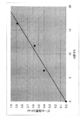
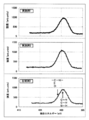
- the schematic of the copper clad laminated board which shows an example of this invention which formed the tie-coat layer, the copper sputtering layer, and the electrolytic copper plating layer on both surfaces of the liquid crystal polymer film. It is a figure which shows the relationship between the power density and surface composition (C, N, O, F) of the plasma processing of an Example. It is a figure which shows the relationship between the nitrogen atom% of a film surface, and peel strength. It is a figure which shows the spectrum of C1s of Examples 1, 2 and Comparative Examples 1, 2. It is a figure which shows the spectrum of N1s of Examples 1, 2 and Comparative Example 1. It is a figure which shows the spectrum of O1s of Examples 1, 2 and Comparative Examples 1, 2.
- the liquid crystal polymer film-based copper-clad laminate according to the present invention provides adhesion to the metal conductor layer on both sides or one side of the liquid crystal polymer film as shown in FIG.
- Plasma treatment is performed, and a barrier layer is applied to a metal or alloy having a barrier effect by a dry plating method or a wet plating method such as a sputtering method or a vapor deposition method.
- a conductor layer of copper or copper alloy is stacked on the barrier layer by a dry plating method such as sputtering or vapor deposition, or a conductive layer is formed by a wet plating method such as electroless copper plating or electrolytic copper plating.
- a dry plating method such as sputtering or vapor deposition
- a conductive layer is formed by a wet plating method such as electroless copper plating or electrolytic copper plating.
- liquid crystal polymer there are a rheotropic liquid crystal polymer represented by aromatic polyamide and a thermotropic liquid crystal polymer represented by aromatic polyester.
- the copper-clad laminate is preferably a thermotropic liquid crystal polymer that has low moisture absorption and a small dimensional change rate due to moisture absorption.
- This thermotropic liquid crystal polymer is classified as a super engineering plastic excellent in heat resistance, although it is inferior in heat resistance to polyimide and aromatic polyamide as a thermoplastic resin.
- thermotropic liquid crystal polymer film used in the present invention a type comprising p-hydroxybenzoic acid and polyethylene terephthalate, a type comprising p-hydroxybenzoic acid and terephthalic acid, 4,4′-dihydroxybiphenyl, p-hydroxybenzoic acid And a type comprising 2,6-hydroxynaphthoic acid have been developed and are commercially available.
- liquid crystal polymer film films such as Bexter CT-Z, CT-F, FB, and OC are commercially available from Kuraray, and films such as BIAC BA and BC are commercially available from Japan Gore-Tex. It will be readily understood that the materials as described above can be used, but are not limited to these types.
- the liquid crystal polymer film is subjected to plasma treatment for adhesion to the metal conductor layer.
- This plasma treatment does not expect the anchor effect due to the increase in surface roughness by applying it, but the surface roughness hardly changes, that is, by strengthening the chemical bond between polymer and metal. It is important to provide adhesion.
- the increase in surface roughness has a negative effect on transmission loss in the high-frequency region, and the surface roughness must be reduced in order to obtain the intended high-frequency characteristics with a copper-clad laminate using liquid crystal polymer. Is desirable.
- the plasma treatment with nitrogen gas of the present invention is to form a new polymer-metal bond by introducing nitrogen originally not present in the liquid crystal polymer film.
- the plasma gas pressure when the gas pressure is low, the plasma discharge becomes unstable and cannot be processed.
- the gas pressure when the gas pressure is high, the plasma discharge is stabilized, but the leak gas increases and the gas is wasted. Even if the gas pressure is increased unnecessarily, it is not economical. Therefore, it can be said that the gas pressure is preferably 2.6 to 15 Pa.
- the present invention performs surface modification of the liquid crystal polymer film by performing plasma treatment in nitrogen gas.
- the nitrogen atom% on the surface of the liquid crystal polymer film is changed to 10 atom%.
- the ratio of nitrogen atom / carbon atom can be 0.13 or more, and the ratio of nitrogen atom / oxygen atom can be 0.7 or more. It has become possible to dramatically improve the adhesion. This process and phenomenon does not exist in the prior art and can be said to be novel.
- the tie coat layer shown in FIG. 1 corresponds to a barrier layer, but a metal such as nickel, cobalt, or chromium that exhibits a barrier effect, or a nickel alloy, cobalt alloy, or chromium alloy is preferable. These have lower conductivity than copper of the conductor layer, and in the high frequency region, current flows through the surface due to the skin effect, and the tie coat layer greatly contributes as a resistance layer.
- tie coat layer As a copper clad laminate for printed circuit boards, if there is no barrier layer such as a tie coat layer, copper will be a polymer in the long term. It may diffuse to the side and cause adverse effects such as breaking the bond. Therefore, in practice, it is desirable that the tie coat layer is made as thin as possible from a metal or alloy having a high conductivity. Moreover, this tie coat layer does not need to be applied when it is considered unnecessary depending on the use conditions of the element.
- a sputtering method, a vapor deposition method, an electroless plating method, or the like can be applied to the tie coat layer, but it is industrially easier to apply sputtering in the same chamber as the plasma treatment in a series of flows from the plasma treatment.
- a metal conductor layer for allowing an original current to flow is formed.
- a copper layer can be formed by a sputtering method.
- the target copper thickness exceeds 1 ⁇ m, it is disadvantageous in cost to form a metal conductor layer to a prescribed copper thickness by sputtering, and in that case, several hundred nm of sputtering is performed on the tie coat layer.
- it can be said that it is preferable to perform copper plating to a prescribed copper thickness by a wet plating method.
- the surface roughness of the liquid crystal polymer film can be reduced to an arithmetic average roughness Ra of 0.15 ⁇ m or less and a root mean square roughness Rq of 0.20 ⁇ m or less.
- the plasma treatment is not an essential purpose to roughen the surface of the liquid crystal polymer film.
- the surface roughness of the liquid crystal polymer film needs to be at least an arithmetic average roughness Ra of 0.05 ⁇ m or more, preferably 0.1 ⁇ m or more.
- the transmission loss per unit length of the copper-clad laminate is set to 20 dB / m or less at 5 GHz, 50 dB / m or less at 20 GHz, and further to 130 dB / m or less at 40 GHz. be able to.
- Example 1 As the liquid crystal polymer film, BIAC BC 50 ⁇ m manufactured by Japan Gore-Tex was used.
- the liquid crystal polymer film was plasma-treated at a gas pressure of 13 Pa and a power density of 4.3 in a nitrogen atmosphere.
- the plasma intensity is expressed in terms of power density, the process conditions such as target size, current-voltage characteristics, and processing speed differ depending on the individual device, so it is meaningless to define the applied voltage and processing time as a whole.
- the power density when the condition for plasma treatment of the polyimide film was 1 was described.
- the surface shape of the liquid crystal polymer film after the plasma treatment was measured with a surface shape measuring instrument of Wyco NT1100 manufactured by Veeco, in a field of view of 120 ⁇ m ⁇ 92 ⁇ m, and arithmetic mean roughness Ra and root mean square roughness Rq was determined.
- the liquid crystal polymer film after the plasma treatment was formed by sputtering to form a Cr tie coat layer having a thickness of 3 nm and a copper sputter layer having a wet plating seed layer having a thickness of 200 nm. Thereafter, a copper layer was grown to 18 ⁇ m by electrolytic plating on the copper sputtered layer to prepare a sample.
- the sample was measured for peel strength for evaluation of adhesion.
- a pattern having a width of 3 mm was formed with a copper chloride etching solution, and then the peel strength was measured using a bond tester 4000 manufactured by Dage.
- Table 1 shows the results of surface roughness and peel strength.
- the surface roughness was Ra 0.10 ⁇ m, Rq 0.14 ⁇ m, and the peel strength was 0.88 kN / m. Although the film surface roughness was small, it was possible to obtain a good peel strength at a level with no practical problem.
- Example 2 The conditions were the same as in Example 1 except that the power density of the plasma treatment was 2.6.
- the results are similarly shown in Table 1.
- the surface roughness is Ra 0.11 ⁇ m, Rq 0.15 ⁇ m, and even if the power density is reduced, the surface roughness is not much different, but the peel strength is 0.57 kN / m, and the power density With the decrease, the peel strength also decreased. However, it shows a peel strength of 0.5 kN / m, and it can be said that there is no practical problem.
- Example 3 The conditions were the same as in Example 1 except that the gas pressure for plasma treatment was 3 Pa. The results are similarly shown in Table 1. As shown in Table 1, the surface roughness was Ra 0.11 ⁇ m, Rq 0.14 ⁇ m, and the peel strength was 0.90 kN / m, which was a satisfactory peel strength at a level that was practically acceptable.
- Example 4 The conditions were the same as in Example 3 except that the tie coat layer was NiCr. The results are similarly shown in Table 1. As shown in Table 1, the surface roughness was Ra 0.11 ⁇ m, Rq 0.14 ⁇ m, and the peel strength was 0.85 kN / m, which was not significantly different from Example 3.
- Example 5 The conditions were the same as in Example 1 except that the liquid crystal polymer film was CT-Z 50 ⁇ m manufactured by Kuraray. The results are similarly shown in Table 1. As shown in Table 1, the surface roughness was Ra 0.10 ⁇ m, Rq 0.15 ⁇ m, and the peel strength was 0.80 kN / m. It was shown that good peel strength can be obtained even when the film is changed.
- Example 1 The conditions were the same as in Example 1 except that the power density of the plasma treatment was 1.3. The results are similarly shown in Table 1. As shown in Table 1, the surface roughness was Ra 0.10 ⁇ m and Rq 0.14 ⁇ m. This is the same as in Example 1, but the peel strength was as poor as 0.40 kN / m, and it was lowered to a level where it was difficult to judge whether it could withstand practical use as a printed wiring material. It has been clarified that the lower the power density, the smaller the peel strength.
- Example 2 The conditions were the same as in Example 1 except that no power was applied during the plasma treatment and the gas was passed through the treatment gas. The results are similarly shown in Table 1. As shown in Table 1, the surface roughness was Ra 0.11 ⁇ m and Rq 0.15 ⁇ m, and the surface roughness of the original film was maintained. The peel strength is that when a tie coat layer and a copper sputter layer are formed on a liquid crystal polymer that is not plasma-treated and the copper layer is grown by electrolytic plating, the adhesion between the liquid crystal polymer and the metal conductor layer is insufficient. I could not do it.
- Example 3 The conditions were the same as in Example 1 except that the plasma treatment gas species was oxygen. The results are similarly shown in Table 1. As shown in Table 1, the surface roughness was the same as in Example 1, but the peel strength was 0.55 kN / m, which was lower than that sputtered with nitrogen. In a liquid crystal polymer film, it can be said that oxygen gas in plasma treatment is less effective in improving film / metal adhesion than nitrogen gas.
- Example 4 As the polyimide film, Kapton E 50 ⁇ m manufactured by DuPont was used as the polyimide film, and the conditions were the same as in Example 1 except that oxygen gas, power density 1, and gas pressure 10 Pa, which are standard plasma treatments for polyimide, were used. .
- the results are similarly shown in Table 1.
- the surface roughness was Ra 0.04 ⁇ m and Rq 0.06 ⁇ m, and the surface of the original polyimide film was small, but the peel strength was as high as 0.99 kN / m.
- it since it is not a liquid crystal polymer film, it cannot be used as a material applied to a high-frequency circuit board or a high-speed transmission line circuit.
- Comparative Example 5 When a liquid crystal polymer is used as a copper clad laminate, thermal lamination is performed as a general method.
- the comparative example 5 is a result at the time of using a rolled copper foil (JX Nippon Mining & Metals Co., Ltd. BHY 18 micron) as a copper clad laminated board produced by thermal lamination. The results are similarly shown in Table 1.
- Table 1 By heat laminating the rolled copper foil, the surface roughness of the film reflected the surface shape of the rolled copper foil, and the surface roughness increased as shown in Table 1.
- the applied liquid crystal polymer film is not subjected to plasma treatment, and the roughening treatment of the copper foil bites into the softened film.
- the anchor effect is the main component of adhesion, strong adhesion cannot be obtained, peel strength is 0.3 kN / m, and sufficient adhesion cannot be obtained.
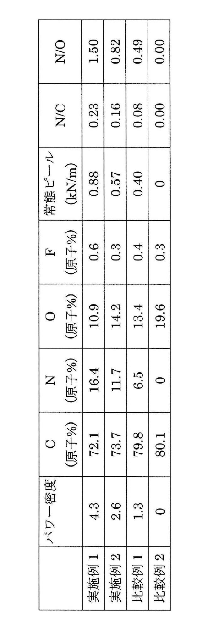
- Example 1 and Example 2 As a means for evaluating the degree of surface modification when changing the power density of plasma treatment in a nitrogen atmosphere, the results of XPS analysis performed on Example 1 and Example 2, and Comparative Example 1 and Comparative Example 2 are shown. Table 2 shows.
- XPS measurement 5600MC manufactured by ULVAC-PHI Co., Ltd. was used as a measuring device. The implementation conditions are as follows. Ultimate vacuum: 2.0 ⁇ 10 ⁇ 9 Torr, Excitation source: Monochromatic AlK ⁇ Output: 210W Detection area: 800 ⁇ m 2 Incident angle: 45 degrees Extraction angle: 45 degrees, sputtering conditions using neutralizing gun, ion species: Ar + , acceleration voltage: 3 kV, sweep area: 3 mm ⁇ 3 mm
- FIG. 2 shows the surface composition shown in Table 2 and shows the relationship between the atomic% of carbon, nitrogen, oxygen, and fluorine and the power density of the plasma treatment. Originally, when the power density was zero, the nitrogen atom% was also zero, but it can be seen that the nitrogen atom% increased as the power density increased.
- FIG. 3 shows the relationship between the nitrogen atom% and the peel strength shown in Table 2. It can be seen that the peel strength increases as the surface modification progresses and the nitrogen atom% increases.
- FIGS. FIG. 4 shows an example of carbon, but in Comparative Example 2 where the power density is zero, two peaks near 285 eV and 288 eV are recognized. The vicinity of 285 eV is a peak due to —C—C— or —C—H, and the power density increased and the peak intensity decreased in the order of Comparative Example 1, Example 2, and Example 1.
- the peak near 285 eV becomes broad, and the intensity due to —C—O— or —CN— near 287 eV increases. is there.
- the peak around 288 eV is a peak due to —C ( ⁇ O) —, but no significant change in power density is observed compared to the decrease in the peak near 285 eV.
- FIG. 5 shows an example of nitrogen, but nitrogen is not detected in Comparative Example 2 where the power density is zero. There is no clear difference in the peak around 400 eV in Comparative Example 1, Example 2, and Example 1.
- FIG. 6 shows an example of oxygen.
- Comparative Example 2 where the power density is zero, peaks are observed near 532 eV and 533 eV. However, as the power density increases, the peak near 533 eV disappears and 532 to 533 eV. The peaks appear to change in between. This peak position is attributed to the bond of O and N such as nitrate.
- the surface of the liquid crystal polymer film was subjected to plasma treatment under a nitrogen atmosphere at a gas pressure of 2.6 to 15 Pa.
- the surface roughness of the film was an arithmetic average roughness Ra of 0.15 ⁇ m or less, and a square average
- the nitrogen atom% on the liquid crystal polymer film surface is 10 atom% or more, and the ratio of nitrogen atom / carbon atom is 0.13.
- the liquid crystal polymer film surface can be modified so that the ratio of nitrogen atom / oxygen atom is 0.7 or more.
- copper-clad laminates with metal conductor layers formed by dry plating, wet plating, or both dry plating and wet plating can provide good adhesion between polymer and tie coat metal, and have good peel strength New printed wiring materials can be provided.
- the surface of the liquid crystal polymer film of the present invention is subjected to a plasma treatment in an oxygen atmosphere or a nitrogen atmosphere at a gas pressure of 2.6 to 15 Pa, and the surface modification is performed so that the nitrogen atom content of the plasma-treated surface is 10 atomic% or more.
- the copper-clad laminate in which the metal conductor layer formed by dry plating and / or wet plating is formed on the surface of the liquid crystal polymer film subjected to the plasma treatment has an interface roughness between the liquid crystal polymer and the metal conductor layer. By maintaining the same roughness as the original film roughness and strengthening the chemical adhesion by plasma treatment, it has an excellent effect that it can provide a copper-clad laminate of liquid crystal polymer with excellent high frequency characteristics. It can be applied to high-frequency circuit boards and high-speed transmission line circuits.
Landscapes
- Chemical & Material Sciences (AREA)
- Engineering & Computer Science (AREA)
- Organic Chemistry (AREA)
- Manufacturing & Machinery (AREA)
- Microelectronics & Electronic Packaging (AREA)
- Materials Engineering (AREA)
- Crystallography & Structural Chemistry (AREA)
- Medicinal Chemistry (AREA)
- Polymers & Plastics (AREA)
- Health & Medical Sciences (AREA)
- Chemical Kinetics & Catalysis (AREA)
- Laminated Bodies (AREA)
- Manufacturing Of Printed Wiring (AREA)
- Parts Printed On Printed Circuit Boards (AREA)
- Other Surface Treatments For Metallic Materials (AREA)
- Physical Vapour Deposition (AREA)
Abstract
Description
しかし、液晶ポリマーと金属導体層の密着性や親和性が乏しいため、金属導体層として一般的に用いられる銅箔の表面粗さを粗くする、又は粗化処理の粒子形状を変更することによって、アンカー効果により物理的な密着を強化しているのが現状である。
特許文献3には、タイコート層に窒素原子を0.5~4.8原子%を固溶させることにより、絶縁フィルムと銅層の密着強度を得る方法が示されているが、プラズマ処理での絶縁フィルム表面改質については記載がない。
1)液晶ポリマーフィルムの片面又は両面の表面の窒素原子の含有量が10原子%以上であり、該液晶ポリマーフィルムの該窒素原子の含有量が10原子%以上である表面上に、乾式めっき及び/又は湿式めっきにより形成された金属導体層を有することを特徴とする液晶ポリマーフィルムベース銅張積層板
2)前記液晶ポリマーフィルムの片面又は両面の表面の窒素原子の含有量が10原子%以上であり、窒素原子/炭素原子の比が0.13以上であることを特徴とする上記1)記載の液晶ポリマーフィルムベース銅張積層板
3)前記液晶ポリマーフィルムの片面又は両面の表面の窒素原子の含有量が10原子%以上であり、窒素原子/酸素原子の比が0.7以上であることを特徴とする上記1)又は2)記載の液晶ポリマーフィルムベース銅張積層板
4)液晶ポリマーフィルムの表面粗さが、算術平均粗さRaが0.15μm以下であり、かつ二乗平均平方根粗さRqが0.20μm以下であることを特徴とする上記1)~3)のいずれか一項に記載の液晶ポリマーフィルムベース銅張積層板
5)前記液晶ポリマーフィルムの表面と乾式めっき及び/又は湿式めっきにより形成された金属導体層との間に、バリア層を有することを特徴とする上記1)~4)のいずれか一項に記載の液晶ポリマーフィルムベース銅張積層板
6)バリア層が、ニッケル若しくはニッケル合金、コバルト若しくはコバルト合金、又はクロム若しくはクロム合金からなるタイコート層であることを特徴とする上記5)記載の液晶ポリマーフィルムベース銅張積層板
7)前記金属導体層が、銅スパッタリング層及び該スパッタリング層の上に形成された電解銅めっき層であることを特徴とする上記1)~6)のいずれか一項に記載の液晶ポリマーフィルムベース銅張積層板、を提供する。
8)液晶ポリマーフィルムの片面または両面の表面を、2.6~15Paのガス圧の窒素雰囲気下でプラズマ処理し、窒素原子の含有量を10原子%以上とした後、該プラズマ処理した液晶ポリマーフィルム面上に、乾式めっき及び/又は湿式めっきにより金属導体層を形成することを特徴とする液晶ポリマーフィルムベース銅張積層板の製造方法
9)前記プラズマ処理した液晶ポリマーフィルム面の窒素原子/炭素原子の比を0.13以上とすることを特徴とする上記8)記載の液晶ポリマーフィルムベース銅張積層板の製造方法
10)前記プラズマ処理した液晶ポリマーフィルム面の窒素原子/酸素原子の比を0.7以上とすることを特徴とする上記8)又は9)記載の液晶ポリマーフィルムベース銅張積層板の製造方法
11)液晶ポリマーフィルムをプラズマ処理することにより、液晶ポリマーフィルムの表面粗さを、算術平均粗さRaを0.15μm以下に、かつ二乗平均平方根粗さRqを0.20μm以下にすることを特徴とする上記8)~10)のいずれか一項に記載の液晶ポリマーフィルムベース銅張積層板の製造方法
12)プラズマ処理された液晶ポリマーフィルムの表面と乾式めっき及び/又は湿式めっきにより形成された金属導体層との間に、バリア層を形成することを特徴とする上記8)~11)のいずれか一項に記載の液晶ポリマーフィルムベース銅張積層板
13)バリア層として、ニッケル若しくはニッケル合金、コバルト若しくはコバルト合金、又はクロム若しくはクロム合金からなるタイコート層を形成することを特徴とする上記12)記載の液晶ポリマーフィルムベース銅張積層板の製造方法
14)前記金属導体層として、予め銅スパッタリング層を形成し、このスパッタリング層上に電解銅めっき層を形成することを特徴とする上記8)~13)のいずれか一項に記載の液晶ポリマーフィルムベース銅張積層板の製造方法、を提供する。
銅張積層板としては、吸湿が少なく、吸湿による寸法変化率が小さいサーモトロピック液晶ポリマーが好ましい。このサーモトロピック液晶ポリマーは、熱可塑性樹脂としてはポリイミドや芳香族ポリアミドには耐熱性は劣るが、耐熱性に優れたスーパーエンジニアリングプラスチックに分類される。
本発明に使用するサーモトロピック液晶ポリマーフィルムについては、p-ヒドロキシ安息香酸とポリエチレンテレフタレートからなるタイプ、p-ヒドロキシ安息香酸とテレフタル酸,4,4’―ジヒドロキシビフェニルからなるタイプ、p-ヒドロキシ安息香酸と2,6―ヒドロキシナフトエル酸からなるタイプなどが開発され、市販されている。
表面粗さの増大は、高周波領域での伝送損失に対して負の効果を示し、液晶ポリマーを用いた銅張積層板で本来目的とする高周波特性を得るために、表面粗さは小さくすることが望ましい。
この窒素ガス雰囲気下でプラズマ処理をすることで、ポリマーと金属の密着性をより強固することが可能である。プラズマガス圧については、ガス圧が低い場合、プラズマ放電が不安定になり、処理することができなくなる。
一方、ガス圧が高い場合、プラズマ放電は安定化するが、リークガスが多くなりガスの無駄となり、むやみにガス圧を高くしても経済的にも良くない。したがって、2.6~15Paのガス圧にするのが望ましいと言える。
このため、現実的にはタイコート層は導電率が大きな金属又は合金を、できるだけ薄くすることが望ましい。また、このタイコート層は、素子の使用条件によって、不必要と考えられる場合には、施工する必要はない。
タイコート層はスパッタリング法、蒸着法、無電解めっき法などが適用できるが、プラズマ処理からの一連の流れの中で、プラズマ処理と同一チャンバー内でスパッタリングする方が、工業的に適用し易い。
しかし、目的とする銅厚が1μmを超える場合、スパッタリング法で規定の銅厚に金属導体層を形成するのはコスト的に不利であり、その場合、タイコート層上にスパッタリングで数百nmの銅シード層を形成後、湿式めっき法で規定の銅厚まで銅めっきする方が好ましいと言える。
この表面粗さの程度からみても、プラズマ処理が液晶ポリマーフィルムの表面を粗くすることが本質的な目的でないことが理解されるであろう。ただし、銅層の密着性を得るためには、液晶ポリマーフィルムの表面粗さとして、少なくとも算術平均粗さRa0.05μm以上、好ましくは0.1μm以上が必要である。
以上の処理によって、銅張積層板の単位長さあたりの伝送損失を、5GHzで20dB/m以下とすること、また20GHzで50dB/m以下とすること、さらには40GHzで130dB/m以下とすることができる。
液晶ポリマーフィルムとしては、ジャパンゴアテックス社製のBIAC BC 50μmを使用した。液晶ポリマーフィルムを窒素雰囲気で、ガス圧13Pa、パワー密度4.3でプラズマ処理を施した。
プラズマの強度をパワー密度で表現したが、個々の装置によりターゲットのサイズや電流―電圧特性、処理速度などのプロセス条件が異なるため、一概に印加電圧と処理時間で定義しても無意味なため、ポリイミドフィルムをプラズマ処理する条件を1とした場合のパワー密度として記載した。
プラズマ処理後の液晶ポリマーフィルムは、スパッタリングによりCrタイコート層を3nmと湿式めっきの種層になる銅スパッタ層を200nm形成した。その後、銅スパッタ層上に電解めっきで銅層を18μmまで成長させ、試料を作製した。
表1に、表面粗さ、ピール強度の結果を示す。表面粗さは、Ra0.10μm、Rq0.14μmとなり、ピール強度は0.88kN/mとなった。フィルム表面粗さは小さいにもかかわらず、実用上問題ないレベルの良好なピール強度を得ることができた。

プラズマ処理のパワー密度を2.6とした以外、実施例1と同条件とした。この結果を同様に、表1に示す。表1に示すように表面粗さは、Ra0.11μm、Rq0.15μmであり、パワー密度が小さくなっても表面粗さに大差ないが、ピール強度は0.57kN/mであり、パワー密度の低下に伴い、ピール強度も低下した。しかし、0.5kN/mのピール強度を示しており、実用上問題がないレベルと言える。
プラズマ処理のガス圧を3Paにした以外、実施例1と同条件とした。この結果を同様に、表1に示す。表1に示すように表面粗さは、Ra0.11μm、Rq0.14μmであり、ピール強度は0.90kN/mと、実用上問題ないレベルの良好なピール強度を得ることができた。
タイコート層をNiCrにした以外、実施例3と同条件とした。この結果を同様に、表1に示す。表1に示すように表面粗さは、Ra0.11μm、Rq0.14μmであり、ピール強度は0.85kN/mとなり、実施例3と大差ない結果となった。
液晶ポリマーフィルムを、クラレ社製CT-Z 50μmとした以外、実施例1と同条件とした。この結果を同様に、表1に示す。表1に示すように表面粗さは、Ra0.10μm、Rq0.15μmであり、ピール強度は0.80kN/mであった。フィルムを変更しても、良好なピール強度が得られることが示された。
プラズマ処理のパワー密度を1.3とした以外、実施例1と同条件とした。この結果を同様に、表1に示す。表1に示すように表面粗さは、Ra0.10μm、Rq0.14μmとなった。これは実施例1と同じであるが、ピール強度は0.40kN/mと悪くなり、プリント配線材として実用に耐え得るか、どうか、判断が困難なレベルまで、低下した。パワー密度が小さいことがピール強度を小さくすることが明らかとなった。
プラズマ処理中にパワーを掛けず、処理ガス中を通過させたこと以外、実施例1と同条件とした。この結果を同様に、表1に示す。表1に示すように、表面粗さは、Ra0.11μm、Rq0.15μmであり、元々のフィルムの表面粗さのままであった。
ピール強度は、プラズマ処理をしない液晶ポリマーにタイコート層、銅スパッタ層を形成して、電解めっきで銅層を成長させる際、液晶ポリマーと金属導体層の密着力が不十分であり、電解めっきをすることができなかった。
プラズマ処理のガス種を酸素にした以外、実施例1と同条件とした。この結果を同様に、表1に示す。表1に示すように表面粗さは実施例1と変わりないが、ピール強度は0.55kN/mとなり、窒素でスパッタしたものより低くなった。液晶ポリマーフィルムにおいて、プラズマ処理での酸素ガスは、窒素ガスに比べ、フィルム/金属間の密着性を向上させる効果が小さいと言える。
フィルムには、ポリイミドフィルムとして、DuPont社製のカプトンE 50μmを使用し、ポリイミドの標準的なプラズマ処理である酸素ガス、パワー密度1、ガス圧10Paにした以外、実施例1と同条件とした。この結果を同様に、表1に示す。
表1に示すように、表面粗さはRa0.04μm、Rq0.06μmであり、元々のポリイミドフィルムの粗さの小さな表面であるが、ピール強度は0.99kN/mと高い値を示した。しかし、液晶ポリマーフィルムではないので、高周波回路基板や高速伝送路用回路へ適用する材料として使用できない。
液晶ポリマーを銅張積層板として使用する際、一般的な方法として熱ラミネーションが行われる。比較例5は、熱ラミネーションで作製された銅張積層板として、圧延銅箔(JX日鉱日石金属株式会社製 BHY 18ミクロン)を使用した場合の結果である。この結果を同様に、表1に示す。
圧延銅箔を熱ラミネーションすることで、フィルムの表面粗さは圧延銅箔の表面形状を反映する結果となり、表1に示すように表面粗さは大きくなった。
到達真空度:2.0×10⁻⁹Torr、
励起源:単色化 AlKα
出力:210W
検出面積:800μm2
入射角:45度
取り出し角:45度、中和銃を使用
スパッタ条件、イオン種:Ar+、加速電圧:3kV、掃引領域:3mm×3mm
288eV付近は、-C(=O)-に起因するピークであるが、285eV付近のピークの減少と比べ、パワー密度に対する大きな変化は認められない。
その後、乾式めっき、または湿式めっき、あるいは乾式めっきと湿式めっきの両方で金属導体層を形成した銅張積層板はポリマーとタイコート金属間の良好な密着性を得ることができ、ピール強度が良好なプリント配線材料を提供することが可能となった。
Claims (14)
- 液晶ポリマーフィルムの片面又は両面の表面の窒素原子の含有量が10原子%以上であり、該液晶ポリマーフィルムの該窒素原子の含有量が10原子%以上である表面上に、乾式めっき及び/又は湿式めっきにより形成された金属導体層を有することを特徴とする液晶ポリマーフィルムベース銅張積層板。
- 前記液晶ポリマーフィルムの片面又は両面の表面の窒素原子の含有量が10原子%以上であり、窒素原子/炭素原子の比が0.13以上であることを特徴とする請求項1記載の液晶ポリマーフィルムベース銅張積層板。
- 前記液晶ポリマーフィルムの片面又は両面の表面の窒素原子の含有量が10原子%以上であり、窒素原子/酸素原子の比が0.7以上であることを特徴とする請求項1又は2記載の液晶ポリマーフィルムベース銅張積層板。
- 液晶ポリマーフィルムの表面粗さが、算術平均粗さRaが0.15μm以下であり、かつ二乗平均平方根粗さRqが0.20μm以下であることを特徴とする請求項1~3のいずれか一項に記載の液晶ポリマーフィルムベース銅張積層板。
- 前記液晶ポリマーフィルムの表面と乾式めっき及び/又は湿式めっきにより形成された金属導体層との間に、バリア層を有することを特徴とする請求項1~4のいずれか一項に記載の液晶ポリマーフィルムベース銅張積層板。
- バリア層が、ニッケル若しくはニッケル合金、コバルト若しくはコバルト合金、又はクロム若しくはクロム合金からなるタイコート層であることを特徴とする請求項5記載の液晶ポリマーフィルムベース銅張積層板。
- 前記金属導体層が、銅スパッタリング層及び該スパッタリング層の上に形成された電解銅めっき層であることを特徴とする請求項1~6のいずれか一項に記載の液晶ポリマーフィルムベース銅張積層板。
- 液晶ポリマーフィルムの片面または両面の表面を、2.6~15Paのガス圧の窒素雰囲気下でプラズマ処理し、窒素原子の含有量を10原子%以上とした後、該プラズマ処理した液晶ポリマーフィルム面上に、乾式めっき及び/又は湿式めっきにより金属導体層を形成することを特徴とする液晶ポリマーフィルムベース銅張積層板の製造方法。
- 前記プラズマ処理した液晶ポリマーフィルム面の窒素原子/炭素原子の比を0.13以上とすることを特徴とする請求項8記載の液晶ポリマーフィルムベース銅張積層板の製造方法。
- 前記プラズマ処理した液晶ポリマーフィルム面の窒素原子/酸素原子の比を0.7以上とすることを特徴とする請求項8又は9記載の液晶ポリマーフィルムベース銅張積層板の製造方法。
- 液晶ポリマーフィルムをプラズマ処理することにより、液晶ポリマーフィルムの表面粗さを、算術平均粗さRaを0.15μm以下に、かつ二乗平均平方根粗さRqを0.20μm以下にすることを特徴とする請求項8~10のいずれか一項に記載の液晶ポリマーフィルムベース銅張積層板の製造方法。
- プラズマ処理された液晶ポリマーフィルムの表面と乾式めっき及び/又は湿式めっきにより形成された金属導体層との間に、バリア層を形成することを特徴とする請求項8~11のいずれか一項に記載の液晶ポリマーフィルムベース銅張積層板。
- バリア層として、ニッケル若しくはニッケル合金、コバルト若しくはコバルト合金、又はクロム若しくはクロム合金からなるタイコート層を形成することを特徴とする請求項12記載の液晶ポリマーフィルムベース銅張積層板の製造方法。
- 前記金属導体層として、予め銅スパッタリング層を形成し、このスパッタリング層上に電解銅めっき層を形成することを特徴とする請求項8~13のいずれか一項に記載の液晶ポリマーフィルムベース銅張積層板の製造方法。
Priority Applications (5)
| Application Number | Priority Date | Filing Date | Title |
|---|---|---|---|
| JP2013502234A JP5639258B2 (ja) | 2011-03-01 | 2012-02-15 | 液晶ポリマーフィルムベース銅張積層板及びその製造方法 |
| EP12752249.8A EP2682264A4 (en) | 2011-03-01 | 2012-02-15 | COPPER-COATED LAMINATE BASED ON A LIQUID CRYSTAL POLYMERIC FILM AND METHOD OF MANUFACTURING THEREOF |
| KR20137025591A KR20130126997A (ko) | 2011-03-01 | 2012-02-15 | 액정 폴리머 필름 베이스 구리 피복 적층판 및 그 제조 방법 |
| US14/000,318 US20140023881A1 (en) | 2011-03-01 | 2012-02-15 | Liquid Crystal Polymer Film Based Copper-Clad Laminate and Method for Producing Same |
| CN201280011305.1A CN103402757B (zh) | 2011-03-01 | 2012-02-15 | 基于液晶聚合物薄膜的覆铜箔层压板及其制造方法 |
Applications Claiming Priority (2)
| Application Number | Priority Date | Filing Date | Title |
|---|---|---|---|
| JP2011-043462 | 2011-03-01 | ||
| JP2011043462 | 2011-03-01 |
Publications (1)
| Publication Number | Publication Date |
|---|---|
| WO2012117850A1 true WO2012117850A1 (ja) | 2012-09-07 |
Family
ID=46757789
Family Applications (1)
| Application Number | Title | Priority Date | Filing Date |
|---|---|---|---|
| PCT/JP2012/053454 Ceased WO2012117850A1 (ja) | 2011-03-01 | 2012-02-15 | 液晶ポリマーフィルムベース銅張積層板及びその製造方法 |
Country Status (7)
| Country | Link |
|---|---|
| US (1) | US20140023881A1 (ja) |
| EP (1) | EP2682264A4 (ja) |
| JP (1) | JP5639258B2 (ja) |
| KR (1) | KR20130126997A (ja) |
| CN (1) | CN103402757B (ja) |
| TW (1) | TWI462827B (ja) |
| WO (1) | WO2012117850A1 (ja) |
Cited By (18)
| Publication number | Priority date | Publication date | Assignee | Title |
|---|---|---|---|---|
| JP2014160738A (ja) * | 2013-02-19 | 2014-09-04 | Sumitomo Metal Mining Co Ltd | めっき積層体の製造方法、及びめっき積層体 |
| JP2016504779A (ja) * | 2012-10-15 | 2016-02-12 | レイセオン カンパニー | 高周波吸収フィルタ |
| WO2019230672A1 (ja) * | 2018-06-01 | 2019-12-05 | 株式会社クラレ | 熱可塑性液晶ポリマー成形体とその製造方法 |
| WO2019244980A1 (ja) * | 2018-06-20 | 2019-12-26 | 国立大学法人大阪大学 | ポリマーと被接着物との接着積層体の製造方法 |
| JP2020029475A (ja) * | 2018-08-20 | 2020-02-27 | 東洋紡株式会社 | 耐熱高分子フィルム、表面処理された耐熱高分子フィルムの製造方法、及び、耐熱高分子フィルムロール |
| JPWO2021039769A1 (ja) * | 2019-08-29 | 2021-03-04 | ||
| JP2021094734A (ja) * | 2019-12-16 | 2021-06-24 | 昭和電工マテリアルズ株式会社 | 積層フィルム、配線基板を製造する方法、及び半導体装置を製造する方法 |
| JP2021098837A (ja) * | 2019-12-23 | 2021-07-01 | 長春人造樹脂廠股▲分▼有限公司 | 液晶ポリマーフィルム及び該液晶ポリマーフィルムを含む積層体 |
| WO2021210478A1 (ja) * | 2020-04-17 | 2021-10-21 | 株式会社クラレ | 金属被覆液晶ポリマーフィルム |
| JP2021182616A (ja) * | 2020-05-15 | 2021-11-25 | プロマティック株式会社 | 積層体の製造方法 |
| WO2021251264A1 (ja) * | 2020-06-09 | 2021-12-16 | 株式会社クラレ | 熱可塑性液晶ポリマー成形体 |
| WO2021251262A1 (ja) * | 2020-06-09 | 2021-12-16 | 株式会社クラレ | 熱可塑性液晶ポリマー成形体 |
| WO2021251265A1 (ja) * | 2020-06-09 | 2021-12-16 | 株式会社クラレ | 熱可塑性液晶ポリマー成形体 |
| WO2021251261A1 (ja) * | 2020-06-09 | 2021-12-16 | 株式会社クラレ | 熱可塑性液晶ポリマー成形体 |
| WO2021251263A1 (ja) * | 2020-06-09 | 2021-12-16 | 株式会社クラレ | 熱可塑性液晶ポリマー成形体 |
| WO2022124687A1 (ko) * | 2020-12-08 | 2022-06-16 | 동우 화인켐 주식회사 | 연성 금속 적층체 및 이의 제조방법 |
| US12103285B2 (en) | 2019-12-23 | 2024-10-01 | Chang Chun Plastics Co., Ltd. | Liquid crystal polymer film and laminate comprising the same |
| WO2024237225A1 (ja) * | 2023-05-16 | 2024-11-21 | 株式会社クラレ | 熱可塑性液晶ポリマーフィルム、金属張積層板および積層体ならびにこれらの製造方法 |
Families Citing this family (15)
| Publication number | Priority date | Publication date | Assignee | Title |
|---|---|---|---|---|
| JP2905134B2 (ja) | 1996-02-29 | 1999-06-14 | 住友重機械工業株式会社 | シートの加熱方法及びその装置 |
| DE112016000328T5 (de) * | 2015-01-13 | 2017-10-19 | Ube Exsymo Co., Ltd. | Flexible Verbundplatte und mehrschichtige Leiterplatte |
| US11220076B2 (en) | 2015-02-19 | 2022-01-11 | Scienstry, Inc. | Laminated switchable panel and methods for making and using |
| WO2016160098A1 (en) * | 2015-04-01 | 2016-10-06 | Means Industries, Inc. | Electronic vehicular transmission and coupling and control assembly for use therein |
| CN113580690B (zh) * | 2016-03-08 | 2023-12-08 | 株式会社可乐丽 | 覆金属层叠板 |
| KR102502200B1 (ko) * | 2016-08-11 | 2023-02-20 | 에스케이넥실리스 주식회사 | 회로 단선/단락을 방지할 수 있는 연성동박적층필름 및 그 제조방법 |
| CN108267870B (zh) * | 2016-12-30 | 2021-03-30 | 财团法人工业技术研究院 | 铜箔复材 |
| KR102136794B1 (ko) * | 2017-03-09 | 2020-07-22 | 케이씨에프테크놀로지스 주식회사 | 우수한 밀착력을 갖는 동박, 그것을 포함하는 전극, 그것을 포함하는 이차전지, 및 그것의 제조방법 |
| JP6764049B1 (ja) | 2018-11-08 | 2020-09-30 | 株式会社クラレ | 熱可塑性液晶ポリマーフィルムおよびそれを用いた回路基板 |
| KR102789044B1 (ko) | 2020-01-29 | 2025-04-01 | 삼성전기주식회사 | 절연 필름 및 이를 포함하는 인쇄회로기판 |
| CN111465217A (zh) * | 2020-03-10 | 2020-07-28 | 深圳市信维通信股份有限公司 | 5g通信用高频柔性基板的制作方法 |
| TW202144601A (zh) * | 2020-05-15 | 2021-12-01 | 日商普羅瑪帝克股份有限公司 | 層壓體的製造方法 |
| JP7354944B2 (ja) * | 2020-07-06 | 2023-10-03 | トヨタ自動車株式会社 | 配線基板の製造方法 |
| JP7456330B2 (ja) | 2020-08-21 | 2024-03-27 | トヨタ自動車株式会社 | 配線基板の製造方法 |
| CN116635235A (zh) * | 2020-12-25 | 2023-08-22 | 株式会社可乐丽 | 具有着色层的热塑性液晶聚合物膜成形体及其制造方法 |
Citations (6)
| Publication number | Priority date | Publication date | Assignee | Title |
|---|---|---|---|---|
| JP2001049002A (ja) | 1999-08-10 | 2001-02-20 | Kuraray Co Ltd | 熱可塑性液晶ポリマーフィルムおよびその製造方法 |
| JP2002501986A (ja) * | 1998-01-30 | 2002-01-22 | イー・アイ・デュポン・ドウ・ヌムール・アンド・カンパニー | 液晶ポリマーのめっき方法およびそれに関連する組成物 |
| JP2003221456A (ja) * | 2002-01-29 | 2003-08-05 | Japan Gore Tex Inc | 高接着性液晶ポリマーフィルム |
| JP2005290370A (ja) * | 2004-03-10 | 2005-10-20 | Matsushita Electric Works Ltd | 金属被覆樹脂成形品およびその製造方法 |
| JP2005297405A (ja) | 2004-04-13 | 2005-10-27 | Sumitomo Metal Mining Co Ltd | 金属被覆液晶ポリマーフィルムの製造方法 |
| WO2008090654A1 (ja) | 2007-01-24 | 2008-07-31 | Sumitomo Metal Mining Co., Ltd. | 2層フレキシブル基板とその製造方法及び該2層フレキシブル基板より得られたフレキシブルプリント配線基板 |
Family Cites Families (16)
| Publication number | Priority date | Publication date | Assignee | Title |
|---|---|---|---|---|
| US5124184A (en) * | 1987-08-21 | 1992-06-23 | Minnesota Mining And Manufacturing Co. | Films containing liquid crystalline polymers |
| JPH0951163A (ja) * | 1995-05-31 | 1997-02-18 | Mitsui Toatsu Chem Inc | フレキシブル回路基板 |
| US6194076B1 (en) * | 1997-04-22 | 2001-02-27 | International Business Machines Corporation | Method of forming adherent metal components on a polyimide substrate |
| JP2000135763A (ja) * | 1998-10-30 | 2000-05-16 | Gunze Ltd | 金属ラミネート用フィルム及びこれを用いたラミネート体 |
| JP2001138446A (ja) * | 1998-12-22 | 2001-05-22 | Tokuyama Corp | 積層体 |
| JP2001138457A (ja) * | 1998-12-25 | 2001-05-22 | Tokuyama Corp | 積層体 |
| JP2002280684A (ja) * | 2001-03-16 | 2002-09-27 | Sumitomo Electric Printed Circuit Inc | フレキシブル銅張回路基板とその製造方法 |
| US20040040148A1 (en) * | 2002-08-29 | 2004-03-04 | Parlex Corporation | Manufacture of flexible printed circuit boards |
| JP2004327931A (ja) * | 2003-04-28 | 2004-11-18 | Matsushita Electric Ind Co Ltd | 金属被膜ポリイミド基板及びその製造方法 |
| JP2005097405A (ja) * | 2003-09-24 | 2005-04-14 | Japan Epoxy Resin Kk | エポキシ樹脂及びそれを用いた塗料用組成物 |
| MY148655A (en) * | 2003-11-27 | 2013-05-15 | Fuji Photo Film Co Ltd | Metal pattern forming method, metal pattern obtained by the same, printed wiring board, conductive film forming method, and conductive film obtained by the same |
| JP4196108B2 (ja) * | 2004-01-27 | 2008-12-17 | パナソニック株式会社 | フレキシブルプリント基板及びフレキシブルプリント基板の製造方法 |
| DE602005014218D1 (de) * | 2004-03-10 | 2009-06-10 | Panasonic Elec Works Co Ltd | Metallbeschichteter harzformkörper und herstellungsverfahren dafür |
| WO2008114539A1 (ja) * | 2007-03-20 | 2008-09-25 | Nippon Mining & Metals Co., Ltd. | 無接着剤フレキシブルラミネート及びその製造方法 |
| JP5587116B2 (ja) * | 2009-09-30 | 2014-09-10 | 京セラ株式会社 | 配線基板及び実装構造体 |
| JP5746866B2 (ja) * | 2011-01-05 | 2015-07-08 | Jx日鉱日石金属株式会社 | 銅張積層板及びその製造方法 |
-
2012
- 2012-02-15 WO PCT/JP2012/053454 patent/WO2012117850A1/ja not_active Ceased
- 2012-02-15 JP JP2013502234A patent/JP5639258B2/ja active Active
- 2012-02-15 EP EP12752249.8A patent/EP2682264A4/en not_active Withdrawn
- 2012-02-15 US US14/000,318 patent/US20140023881A1/en not_active Abandoned
- 2012-02-15 KR KR20137025591A patent/KR20130126997A/ko not_active Ceased
- 2012-02-15 CN CN201280011305.1A patent/CN103402757B/zh not_active Expired - Fee Related
- 2012-02-20 TW TW101105425A patent/TWI462827B/zh not_active IP Right Cessation
Patent Citations (6)
| Publication number | Priority date | Publication date | Assignee | Title |
|---|---|---|---|---|
| JP2002501986A (ja) * | 1998-01-30 | 2002-01-22 | イー・アイ・デュポン・ドウ・ヌムール・アンド・カンパニー | 液晶ポリマーのめっき方法およびそれに関連する組成物 |
| JP2001049002A (ja) | 1999-08-10 | 2001-02-20 | Kuraray Co Ltd | 熱可塑性液晶ポリマーフィルムおよびその製造方法 |
| JP2003221456A (ja) * | 2002-01-29 | 2003-08-05 | Japan Gore Tex Inc | 高接着性液晶ポリマーフィルム |
| JP2005290370A (ja) * | 2004-03-10 | 2005-10-20 | Matsushita Electric Works Ltd | 金属被覆樹脂成形品およびその製造方法 |
| JP2005297405A (ja) | 2004-04-13 | 2005-10-27 | Sumitomo Metal Mining Co Ltd | 金属被覆液晶ポリマーフィルムの製造方法 |
| WO2008090654A1 (ja) | 2007-01-24 | 2008-07-31 | Sumitomo Metal Mining Co., Ltd. | 2層フレキシブル基板とその製造方法及び該2層フレキシブル基板より得られたフレキシブルプリント配線基板 |
Non-Patent Citations (1)
| Title |
|---|
| See also references of EP2682264A4 * |
Cited By (37)
| Publication number | Priority date | Publication date | Assignee | Title |
|---|---|---|---|---|
| JP2016504779A (ja) * | 2012-10-15 | 2016-02-12 | レイセオン カンパニー | 高周波吸収フィルタ |
| JP2014160738A (ja) * | 2013-02-19 | 2014-09-04 | Sumitomo Metal Mining Co Ltd | めっき積層体の製造方法、及びめっき積層体 |
| JP7382926B2 (ja) | 2018-06-01 | 2023-11-17 | 株式会社クラレ | 熱可塑性液晶ポリマー成形体とその製造方法 |
| WO2019230672A1 (ja) * | 2018-06-01 | 2019-12-05 | 株式会社クラレ | 熱可塑性液晶ポリマー成形体とその製造方法 |
| US12233620B2 (en) | 2018-06-01 | 2025-02-25 | Kuraray Co., Ltd. | Thermoplastic liquid crystal polymer molded body and method for manufacturing same |
| JPWO2019230672A1 (ja) * | 2018-06-01 | 2021-07-15 | 株式会社クラレ | 熱可塑性液晶ポリマー成形体とその製造方法 |
| WO2019244980A1 (ja) * | 2018-06-20 | 2019-12-26 | 国立大学法人大阪大学 | ポリマーと被接着物との接着積層体の製造方法 |
| JP7333080B2 (ja) | 2018-06-20 | 2023-08-24 | 国立大学法人大阪大学 | ポリマーと被接着物との接着積層体の製造方法 |
| JPWO2019244980A1 (ja) * | 2018-06-20 | 2021-07-26 | 国立大学法人大阪大学 | ポリマーと被接着物との接着積層体の製造方法 |
| JP7116889B2 (ja) | 2018-08-20 | 2022-08-12 | 東洋紡株式会社 | 耐熱高分子フィルム、表面処理された耐熱高分子フィルムの製造方法、及び、耐熱高分子フィルムロール |
| JP2020029475A (ja) * | 2018-08-20 | 2020-02-27 | 東洋紡株式会社 | 耐熱高分子フィルム、表面処理された耐熱高分子フィルムの製造方法、及び、耐熱高分子フィルムロール |
| WO2021039769A1 (ja) * | 2019-08-29 | 2021-03-04 | 株式会社クラレ | 熱可塑性液晶ポリマー成形体およびその製造方法 |
| JPWO2021039769A1 (ja) * | 2019-08-29 | 2021-03-04 | ||
| JP7520854B2 (ja) | 2019-08-29 | 2024-07-23 | 株式会社クラレ | 熱可塑性液晶ポリマー成形体およびその製造方法 |
| TWI851799B (zh) * | 2019-08-29 | 2024-08-11 | 日商可樂麗股份有限公司 | 熱塑性液晶聚合物成形體及其製造方法 |
| JP2021094734A (ja) * | 2019-12-16 | 2021-06-24 | 昭和電工マテリアルズ株式会社 | 積層フィルム、配線基板を製造する方法、及び半導体装置を製造する方法 |
| JP7447459B2 (ja) | 2019-12-16 | 2024-03-12 | 株式会社レゾナック | 積層フィルム、配線基板を製造する方法、及び半導体装置を製造する方法 |
| JP7312152B2 (ja) | 2019-12-23 | 2023-07-20 | 長春人造樹脂廠股▲分▼有限公司 | 液晶ポリマーフィルム及び該液晶ポリマーフィルムを含む積層体 |
| US11608410B2 (en) | 2019-12-23 | 2023-03-21 | Chang Chun Plastics Co., Ltd. | Liquid crystal polymer film and laminate comprising the same |
| JP2021098837A (ja) * | 2019-12-23 | 2021-07-01 | 長春人造樹脂廠股▲分▼有限公司 | 液晶ポリマーフィルム及び該液晶ポリマーフィルムを含む積層体 |
| US12103285B2 (en) | 2019-12-23 | 2024-10-01 | Chang Chun Plastics Co., Ltd. | Liquid crystal polymer film and laminate comprising the same |
| US11840602B2 (en) | 2019-12-23 | 2023-12-12 | Chang Chun Plastics Co., Ltd. | Laminate, circuit board, and liquid crystal polymer film applied to the same |
| US11945907B2 (en) | 2019-12-23 | 2024-04-02 | Chang Chun Plastics Co., Ltd. | Liquid crystal polymer film and laminate comprising the same |
| US11926698B2 (en) | 2019-12-23 | 2024-03-12 | Chang Chun Plastics Co., Ltd. | Liquid crystal polymer film and laminate comprising the same |
| JPWO2021210478A1 (ja) * | 2020-04-17 | 2021-10-21 | ||
| WO2021210478A1 (ja) * | 2020-04-17 | 2021-10-21 | 株式会社クラレ | 金属被覆液晶ポリマーフィルム |
| US12089327B2 (en) | 2020-04-17 | 2024-09-10 | Kuraray Co., Ltd. | Metal-coated liquid-crystal polymer film |
| JP7378107B2 (ja) | 2020-04-17 | 2023-11-13 | 株式会社クラレ | 金属被覆液晶ポリマーフィルム |
| JP2021182616A (ja) * | 2020-05-15 | 2021-11-25 | プロマティック株式会社 | 積層体の製造方法 |
| WO2021251263A1 (ja) * | 2020-06-09 | 2021-12-16 | 株式会社クラレ | 熱可塑性液晶ポリマー成形体 |
| WO2021251261A1 (ja) * | 2020-06-09 | 2021-12-16 | 株式会社クラレ | 熱可塑性液晶ポリマー成形体 |
| WO2021251265A1 (ja) * | 2020-06-09 | 2021-12-16 | 株式会社クラレ | 熱可塑性液晶ポリマー成形体 |
| WO2021251262A1 (ja) * | 2020-06-09 | 2021-12-16 | 株式会社クラレ | 熱可塑性液晶ポリマー成形体 |
| WO2021251264A1 (ja) * | 2020-06-09 | 2021-12-16 | 株式会社クラレ | 熱可塑性液晶ポリマー成形体 |
| JP2023551840A (ja) * | 2020-12-08 | 2023-12-13 | 東友ファインケム株式会社 | フレキシブル金属積層体およびその製造方法 |
| WO2022124687A1 (ko) * | 2020-12-08 | 2022-06-16 | 동우 화인켐 주식회사 | 연성 금속 적층체 및 이의 제조방법 |
| WO2024237225A1 (ja) * | 2023-05-16 | 2024-11-21 | 株式会社クラレ | 熱可塑性液晶ポリマーフィルム、金属張積層板および積層体ならびにこれらの製造方法 |
Also Published As
| Publication number | Publication date |
|---|---|
| JPWO2012117850A1 (ja) | 2014-07-07 |
| TWI462827B (zh) | 2014-12-01 |
| KR20130126997A (ko) | 2013-11-21 |
| CN103402757B (zh) | 2016-02-10 |
| EP2682264A1 (en) | 2014-01-08 |
| TW201240803A (en) | 2012-10-16 |
| US20140023881A1 (en) | 2014-01-23 |
| JP5639258B2 (ja) | 2014-12-10 |
| CN103402757A (zh) | 2013-11-20 |
| EP2682264A4 (en) | 2014-12-10 |
Similar Documents
| Publication | Publication Date | Title |
|---|---|---|
| JP5639258B2 (ja) | 液晶ポリマーフィルムベース銅張積層板及びその製造方法 | |
| JP5746866B2 (ja) | 銅張積層板及びその製造方法 | |
| TWI766021B (zh) | 氟樹脂膜及積層體以及熱壓積層體之製造方法 | |
| JP3563730B2 (ja) | フレキシブルプリント回路基板 | |
| JP4341023B2 (ja) | 金属被覆液晶ポリマーフィルムの製造方法 | |
| CN108778713B (zh) | 覆金属层压板及其制造方法 | |
| WO2015064437A1 (ja) | 熱可塑性液晶ポリマーフィルムの製造方法、並びに回路基板及びその製造方法 | |
| JP6480289B2 (ja) | 金属蒸着層付き熱可塑性液晶ポリマーフィルムの製造方法、該製造方法を用いた金属蒸着層付き熱可塑性液晶ポリマーフィルム、金属張積層板の製造方法、及び金属張積層板 | |
| WO2018150549A1 (ja) | 金属蒸着層付き熱可塑性液晶ポリマーフィルムの製造方法、該製造方法を用いた金属蒸着層付き熱可塑性液晶ポリマーフィルム、金属張積層板の製造方法、及び金属張積層板 | |
| WO2012108264A1 (ja) | 2層銅張積層材及びその製造方法 | |
| WO2009098832A1 (ja) | 無接着剤フレキシブルラミネート | |
| JP6035679B2 (ja) | めっき積層体の製造方法、及びめっき積層体 | |
| KR101363771B1 (ko) | 2층 플렉시블 기판 및 그 제조 방법 | |
| JP5154055B2 (ja) | 電子回路基板の製造方法 | |
| JP2001049002A (ja) | 熱可塑性液晶ポリマーフィルムおよびその製造方法 | |
| JP7700454B2 (ja) | 金属積層体、および金属積層体の製造方法 | |
| Ahn et al. | Peel strength of sputtered FCCL (flexible copper clad laminate) using Ar: O2 mixed gas preprocessing and a Ni-Cr seed layer | |
| Noh et al. | Effect of Cr thickness on adhesion strength of Cu/Cr/polyimide flexible copper clad laminate fabricated by roll-to-roll process | |
| CN103354843A (zh) | 双层覆铜层压材料及其制造方法 | |
| CN112423983A (zh) | 层叠体及层叠体的制造方法 | |
| JP4086803B2 (ja) | フレキシブルプリント回路基板の製造方法 | |
| Noh et al. | Effects of different kinds of seed layers and heat treatment on adhesion characteristics of Cu/(Cr or Ni–Cr)/PI interfaces in flexible printed circuits | |
| JP7519691B2 (ja) | フレキシブル基板 | |
| Zhang et al. | Advances on the performance and fabrication of low-background PTFE based electronic substrates by surface modification | |
| TW202246053A (zh) | 印刷電路板用積層體及多層印刷電路板用接合體 |
Legal Events
| Date | Code | Title | Description |
|---|---|---|---|
| 121 | Ep: the epo has been informed by wipo that ep was designated in this application |
Ref document number: 12752249 Country of ref document: EP Kind code of ref document: A1 |
|
| DPE1 | Request for preliminary examination filed after expiration of 19th month from priority date (pct application filed from 20040101) | ||
| ENP | Entry into the national phase |
Ref document number: 2013502234 Country of ref document: JP Kind code of ref document: A |
|
| REEP | Request for entry into the european phase |
Ref document number: 2012752249 Country of ref document: EP |
|
| NENP | Non-entry into the national phase |
Ref country code: DE |
|
| ENP | Entry into the national phase |
Ref document number: 20137025591 Country of ref document: KR Kind code of ref document: A |
|
| WWE | Wipo information: entry into national phase |
Ref document number: 14000318 Country of ref document: US |