WO2012117894A1 - Module à semi-conducteur de puissance, procédé de fabrication d'un module à semi-conducteur de puissance et appareil de conversion électrique - Google Patents
Module à semi-conducteur de puissance, procédé de fabrication d'un module à semi-conducteur de puissance et appareil de conversion électrique Download PDFInfo
- Publication number
- WO2012117894A1 WO2012117894A1 PCT/JP2012/054129 JP2012054129W WO2012117894A1 WO 2012117894 A1 WO2012117894 A1 WO 2012117894A1 JP 2012054129 W JP2012054129 W JP 2012054129W WO 2012117894 A1 WO2012117894 A1 WO 2012117894A1
- Authority
- WO
- WIPO (PCT)
- Prior art keywords
- power semiconductor
- heat radiating
- semiconductor module
- case
- circuit body
- Prior art date
- Legal status (The legal status is an assumption and is not a legal conclusion. Google has not performed a legal analysis and makes no representation as to the accuracy of the status listed.)
- Ceased
Links
Images














Classifications
-
- H—ELECTRICITY
- H10—SEMICONDUCTOR DEVICES; ELECTRIC SOLID-STATE DEVICES NOT OTHERWISE PROVIDED FOR
- H10W—GENERIC PACKAGES, INTERCONNECTIONS, CONNECTORS OR OTHER CONSTRUCTIONAL DETAILS OF DEVICES COVERED BY CLASS H10
- H10W40/00—Arrangements for thermal protection or thermal control
- H10W40/20—Arrangements for cooling
- H10W40/22—Arrangements for cooling characterised by their shape, e.g. having conical or cylindrical projections
-
- H—ELECTRICITY
- H02—GENERATION; CONVERSION OR DISTRIBUTION OF ELECTRIC POWER
- H02M—APPARATUS FOR CONVERSION BETWEEN AC AND AC, BETWEEN AC AND DC, OR BETWEEN DC AND DC, AND FOR USE WITH MAINS OR SIMILAR POWER SUPPLY SYSTEMS; CONVERSION OF DC OR AC INPUT POWER INTO SURGE OUTPUT POWER; CONTROL OR REGULATION THEREOF
- H02M3/00—Conversion of DC power input into DC power output
- H02M3/02—Conversion of DC power input into DC power output without intermediate conversion into AC
- H02M3/04—Conversion of DC power input into DC power output without intermediate conversion into AC by static converters
- H02M3/10—Conversion of DC power input into DC power output without intermediate conversion into AC by static converters using discharge tubes with control electrode or semiconductor devices with control electrode
- H02M3/145—Conversion of DC power input into DC power output without intermediate conversion into AC by static converters using discharge tubes with control electrode or semiconductor devices with control electrode using devices of a triode or transistor type requiring continuous application of a control signal
- H02M3/155—Conversion of DC power input into DC power output without intermediate conversion into AC by static converters using discharge tubes with control electrode or semiconductor devices with control electrode using devices of a triode or transistor type requiring continuous application of a control signal using semiconductor devices only
-
- H—ELECTRICITY
- H02—GENERATION; CONVERSION OR DISTRIBUTION OF ELECTRIC POWER
- H02M—APPARATUS FOR CONVERSION BETWEEN AC AND AC, BETWEEN AC AND DC, OR BETWEEN DC AND DC, AND FOR USE WITH MAINS OR SIMILAR POWER SUPPLY SYSTEMS; CONVERSION OF DC OR AC INPUT POWER INTO SURGE OUTPUT POWER; CONTROL OR REGULATION THEREOF
- H02M7/00—Conversion of AC power input into DC power output; Conversion of DC power input into AC power output
- H02M7/42—Conversion of DC power input into AC power output without possibility of reversal
- H02M7/44—Conversion of DC power input into AC power output without possibility of reversal by static converters
- H02M7/48—Conversion of DC power input into AC power output without possibility of reversal by static converters using discharge tubes with control electrode or semiconductor devices with control electrode
-
- H—ELECTRICITY
- H10—SEMICONDUCTOR DEVICES; ELECTRIC SOLID-STATE DEVICES NOT OTHERWISE PROVIDED FOR
- H10W—GENERIC PACKAGES, INTERCONNECTIONS, CONNECTORS OR OTHER CONSTRUCTIONAL DETAILS OF DEVICES COVERED BY CLASS H10
- H10W40/00—Arrangements for thermal protection or thermal control
-
- H—ELECTRICITY
- H10—SEMICONDUCTOR DEVICES; ELECTRIC SOLID-STATE DEVICES NOT OTHERWISE PROVIDED FOR
- H10W—GENERIC PACKAGES, INTERCONNECTIONS, CONNECTORS OR OTHER CONSTRUCTIONAL DETAILS OF DEVICES COVERED BY CLASS H10
- H10W40/00—Arrangements for thermal protection or thermal control
- H10W40/40—Arrangements for thermal protection or thermal control involving heat exchange by flowing fluids
- H10W40/47—Arrangements for thermal protection or thermal control involving heat exchange by flowing fluids by flowing liquids, e.g. forced water cooling
-
- H—ELECTRICITY
- H10—SEMICONDUCTOR DEVICES; ELECTRIC SOLID-STATE DEVICES NOT OTHERWISE PROVIDED FOR
- H10W—GENERIC PACKAGES, INTERCONNECTIONS, CONNECTORS OR OTHER CONSTRUCTIONAL DETAILS OF DEVICES COVERED BY CLASS H10
- H10W72/00—Interconnections or connectors in packages
- H10W72/071—Connecting or disconnecting
-
- H—ELECTRICITY
- H10—SEMICONDUCTOR DEVICES; ELECTRIC SOLID-STATE DEVICES NOT OTHERWISE PROVIDED FOR
- H10W—GENERIC PACKAGES, INTERCONNECTIONS, CONNECTORS OR OTHER CONSTRUCTIONAL DETAILS OF DEVICES COVERED BY CLASS H10
- H10W72/00—Interconnections or connectors in packages
- H10W72/30—Die-attach connectors
-
- H—ELECTRICITY
- H10—SEMICONDUCTOR DEVICES; ELECTRIC SOLID-STATE DEVICES NOT OTHERWISE PROVIDED FOR
- H10W—GENERIC PACKAGES, INTERCONNECTIONS, CONNECTORS OR OTHER CONSTRUCTIONAL DETAILS OF DEVICES COVERED BY CLASS H10
- H10W90/00—Package configurations
-
- H—ELECTRICITY
- H02—GENERATION; CONVERSION OR DISTRIBUTION OF ELECTRIC POWER
- H02M—APPARATUS FOR CONVERSION BETWEEN AC AND AC, BETWEEN AC AND DC, OR BETWEEN DC AND DC, AND FOR USE WITH MAINS OR SIMILAR POWER SUPPLY SYSTEMS; CONVERSION OF DC OR AC INPUT POWER INTO SURGE OUTPUT POWER; CONTROL OR REGULATION THEREOF
- H02M7/00—Conversion of AC power input into DC power output; Conversion of DC power input into AC power output
- H02M7/003—Constructional details, e.g. physical layout, assembly, wiring or busbar connections
-
- H—ELECTRICITY
- H10—SEMICONDUCTOR DEVICES; ELECTRIC SOLID-STATE DEVICES NOT OTHERWISE PROVIDED FOR
- H10W—GENERIC PACKAGES, INTERCONNECTIONS, CONNECTORS OR OTHER CONSTRUCTIONAL DETAILS OF DEVICES COVERED BY CLASS H10
- H10W74/00—Encapsulations, e.g. protective coatings
-
- H—ELECTRICITY
- H10—SEMICONDUCTOR DEVICES; ELECTRIC SOLID-STATE DEVICES NOT OTHERWISE PROVIDED FOR
- H10W—GENERIC PACKAGES, INTERCONNECTIONS, CONNECTORS OR OTHER CONSTRUCTIONAL DETAILS OF DEVICES COVERED BY CLASS H10
- H10W90/00—Package configurations
- H10W90/401—Package configurations characterised by multiple insulating or insulated package substrates, interposers or RDLs
Definitions
- the present invention relates to a power semiconductor module having a power semiconductor element that performs a switching operation for converting DC power into AC power or converting AC power into DC power, a method of manufacturing the power semiconductor module, and a power converter.
- the power converter is a function for converting DC power supplied from a DC power source into AC power for supplying an AC electric load such as a rotating electrical machine, or for supplying AC power generated by the rotating electrical machine to a DC power source. It has a function to convert to DC power.
- the power conversion device includes a power semiconductor device having a power semiconductor element that performs a switching operation. When the power semiconductor element repeats the conduction operation and the interruption operation, power conversion from DC power to AC power or from AC power to DC power is performed.
- Patent Document 1 describes a power semiconductor device in which a power semiconductor element is sealed with a resin material in a state in which a positive electrode side terminal and a negative electrode side terminal are stacked and accommodated in a CAN-shaped case.
- An object of the present invention is to improve the reliability of a power semiconductor device, that is, a power semiconductor module and a power conversion device using the same.
- a power semiconductor module includes a circuit body having a power semiconductor element and a conductor member connected to the power semiconductor element, a case housing the circuit body, the circuit body, A connection member that connects the case, the case being disposed so as to oppose the circuit body so as to sandwich the circuit body, the first heat dissipation member, and the second heat dissipation member. And a middle part formed around the first heat radiating member and connected to the side wall, wherein the intermediate member is curved so as to protrude toward the storage space of the storage member Is formed.
- the connecting portion between the side wall and the intermediate member is defined as a first connecting portion, and the first heat radiating member and the intermediate member
- the connection portion is defined as the second connection portion
- the convex portion formed on the intermediate member is on the side where the circuit body is arranged with respect to the position of the line segment connecting the first connection portion and the second connection portion. It is preferable to form a convex shape.
- the apex of the convex portion is formed at an intermediate portion of a line segment connecting the first connection portion and the second connection portion. Is preferred.
- the apex of the convex portion is higher than the first portion of the line segment connecting the first connection portion and the second connection portion. Preferably, it is formed on the side close to the connecting portion.
- the apex of the convex portion is more than the middle portion of the line segment connecting the first connection portion and the second connection portion. Preferably, it is formed on the side close to the connecting portion.
- the second connection portion is a corner portion of the first heat dissipation member, and the first connection portion is a corner of the intermediate member. Part.
- the projected portion of the convex portion formed on the intermediate member is the first It is preferable to have a shape that bends along two adjacent sides of the first heat radiating member for forming the corners of the two connecting portions.
- the curved portion of the intermediate member is plastically deformed.
- a circuit body having a semiconductor element, a conductor plate connected to an electrode surface of the semiconductor element via solder, and a first heat dissipation facing one surface of the circuit body.
- a power semiconductor module manufacturing method comprising: a metal case having an intermediate member forming an opening; a first step of inserting the circuit body from the opening of the case; the first heat dissipation plate; A second step of deforming a part of the intermediate member of the case so as to sandwich the circuit body by a heat sink; a third step of further deforming a part of the intermediate member of the case; A fourth step of subjecting the circuit body to a high temperature treatment.
- the power semiconductor module joins at least one of the first heat radiating plate and the second heat radiating plate to the circuit body. It is preferable that the adhesive strength of the sheet is increased by the high temperature treatment in the fourth step.
- the power conversion device forms a power semiconductor module including a power semiconductor element that converts a direct current into an alternating current, and a flow path for flowing a coolant for cooling the power semiconductor element.
- the power semiconductor module includes a circuit body having a conductor member connected to the power semiconductor element, a case for housing the circuit body, and a connection for connecting the circuit body and the case.
- a first heat radiating member and a second heat radiating member disposed so as to face each other so as to sandwich the circuit body, and a side wall connecting the first heat radiating member and the second heat radiating member.
- An intermediate member formed around the first heat dissipation member and connected to the side wall, wherein the intermediate member is formed with a curved portion so as to protrude toward the storage space of the storage member Is further the case, the first heat radiation member and the second heat radiating member is fixed to the channel member so as to direct contact with the coolant.
- the first heat radiating member and the intermediate member correspond to the first heat radiating member of one flat planar member of the case. Is preferably formed by being pressed toward the storage space of the storage member.
- the reliability of the power semiconductor module and the power conversion device using the same can be improved.
- FIG. 1 is a system diagram showing a system of a hybrid vehicle.
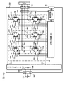
- FIG. 16 is a circuit diagram showing a configuration of an electric circuit shown in FIG. 15. It is an external appearance perspective view of the power converter device 200 as embodiment which concerns on this invention. It is an external appearance perspective view of the power converter device 200 as embodiment which concerns on this invention. It is a figure which shows the state which removed the lid
- FIG. 3 is an external perspective view in which a power module 300U to 300W, a capacitor module 500, and a bus bar assembly 800 are assembled to a flow path forming body 12.
- FIG. The state which removed the bus-bar assembly 800 from the flow-path formation body 12 is shown.
- 3 is a perspective view of a flow path forming body 12.
- FIG. 26A is a perspective view of the power module 300U of the present embodiment.
- FIG. 26B is a cross-sectional view of the power module 300 ⁇ / b> U of the present embodiment cut along a cross section D and viewed from the direction E.
- FIG. 27A is a perspective view
- FIG. 27B is a cross-sectional view taken along the section D and viewed from the direction E similarly to FIG.
- FIG. 27C shows a cross-sectional view before the fin 305 is pressed and the bending portion 304A is deformed.
- FIG. 28A is a perspective view
- FIG. 28B is a cross-sectional view taken along the section D and viewed from the direction E as in FIGS. 26B and 27B.
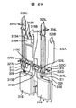
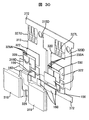
- FIG. 29 is a perspective view of a power module 300U in which the first sealing resin 348 and the wiring insulating portion 608 are further removed from the state shown in FIG. It is a figure for demonstrating the assembly process of the module primary sealing body 302.
- FIG. 1 is an external perspective view of a capacitor module 500.
- FIG. 2 is a perspective view of a bus bar assembly 800.
- FIG. FIG. 4 is a view showing a flow path forming body 12 in which power modules 300U to 300W are fixed to openings 402a to 402c and a capacitor module 500 is stored in a storage space 405.
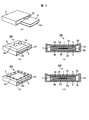
- FIG. 1A is a perspective view of one side of a power semiconductor module (power semiconductor device) 300 according to the first embodiment of the present invention
- FIG. 1B is a perspective view of the other side of the power semiconductor module 300
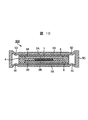
- FIG. 1C is a cross-sectional view of the power semiconductor module 300 taken along the cross-section A shown in FIGS. 1A and 1B and viewed from the direction B.
- the power semiconductor module 300 includes a case 5 that houses a circuit body 100 containing a semiconductor element 1 described later.
- the case 5 has a rectangular parallelepiped shape, and includes a first heat radiating member 5A and a second heat radiating member 5B that form the largest surface, and a side wall 5C that forms a side surface.
- the case 5 is formed with an opening 5G for inserting the circuit body 100 on one of a plurality of side surfaces.
- the first heat radiating member 5 ⁇ / b> A and the second heat radiating member 5 ⁇ / b> B are formed to face each other via the circuit body 100.
- the intermediate member 5D is disposed so as to surround the first heat radiating member 5A, and connects the first heat radiating member 5A and the side wall 5C.
- the intermediate member 5E is disposed so as to surround the second heat radiating member 5B, and connects the second heat radiating member 5B and the side wall 5C.
- Al, Al alloy, Cu, Cu alloy or the like having high thermal conductivity is used.
- a joining member 6 is disposed between the inner wall of the case 5 and the circuit body 100.
- the joining member 6 for example, a resin member having high adhesiveness and insulating properties is used.
- the joining member 6 is preferably an insulating sheet having high adhesiveness and insulating properties.
- solder material a low-temperature sintered bonding material containing fine metal particles, a conductive adhesive containing fine metal particles, or the like for the bonding member 6.
- an insulating member for example, a ceramic member such as aluminum nitride, alumina, silicon nitride, or a laminated material of ceramic and metal is inserted between the circuit body 100 and the case 5. It is necessary to join.
- the circuit body 100 includes a semiconductor element 1, a conductor plate 3 ⁇ / b> A connected to one electrode surface of the semiconductor element 1 via a bonding member 2 ⁇ / b> A, and the other of the semiconductor elements 1.
- a conductive plate 3B connected to the electrode surface and the bonding member 2B, and a sealing material 4 for sealing the semiconductor element 1, the conductive plate 3A, and the conductive plate 3B are provided.
- the sealing material 4 is formed so that the surfaces of the conductor plate 3A and the conductor plate 3B opposite to the side where the semiconductor element 1 is disposed are exposed.
- the semiconductor element 1 is, for example, Si, SiC, GaN or the like.
- the joining members 2A and 2B are, for example, a solder material, a low-temperature sintered joining material containing fine metal particles, and a conductive adhesive containing fine metal particles.
- a solder material for example, Cu, Cu alloy, Al, Al alloy or the like having high electrical conductivity or thermal conductivity is used.
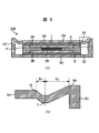
- the intermediate member 5D of the case 5 is formed with a curved portion so as to protrude toward the storage space of the case 5. That is, when the connection portion between the side wall 5C and the intermediate member 5D is defined as the first connection portion 5H, and the connection portion between the first heat radiation member 5A and the intermediate member 5D is defined as the second connection portion 5I, it is formed on the intermediate member 5D.
- the convex portion to be formed has a convex shape on the side where the circuit body 100 is disposed with respect to the position of the line segment connecting the first connection portion 5H and the second connection portion 5I.
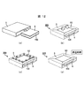
- FIGS. 2A to 2E are diagrams showing an assembly process of the power semiconductor module 300 according to the present embodiment.
- the circuit body 100 to which the joining member 6 is attached is inserted into the case 5 through the opening 5G.
- the joining member 6 is fixed in all or a part of one surface of the circuit body 100 by, for example, metal joining, adhesion, application, or the like, and it is preferable that both the positions do not shift.
- a pressing force is applied in a direction substantially perpendicular to the surface of the first heat radiating member 5A. Accordingly, the intermediate member 5D is deformed, and the joining member 6 and the inner wall of the case 5 are brought into close contact with each other. That is, the first heat radiating member 5A and the intermediate member 5D are formed by pressing a portion corresponding to the first heat radiating member 5A of one flat planar member of the case 5. Moreover, the adhesive force between the joining member 6 and the circuit body 100 is also improved by the pressing force to the first heat radiating member 5A. At this time, a reaction force is generated due to the deformation of the intermediate member 5D.
- FIG. 2C is a cross-sectional view of the power semiconductor module 300 after the completion of the second assembly process.
- FIG. 2D is a cross-sectional view of the power semiconductor module 300 after completion of the third assembly process.
- FIG. 3A is a cross-sectional view of the power semiconductor module 300 of this embodiment
- FIG. 3B is an enlarged view of a dotted line encircled portion in FIG.
- the vertex of the convex portion formed on the intermediate member 5 ⁇ / b> D is defined as the convex vertex portion 7.
- the distance between the first connecting portion 5H and the convex apex portion 7 in the direction parallel to the heat radiating surface of the first heat radiating member 5A is defined as 5J, and the second when projected onto the surface parallel to the first heat radiating member 5A.
- the distance between the connecting portion 5I and the convex portion vertex 7 is defined as 5K.
- the convex portion of the intermediate member 5D is formed so that the distance 5K is larger than the distance 5J.
- FIG. 4 shows the distance from the center position of the intermediate member 5D in the width direction (between the first connecting portion 5H and the second connecting portion 5I) to the convex apex portion 7, and the joining member 6 after the completion of the third assembly step. It is the figure which showed the relationship of stress.
- the convex vertex 7 is formed at the center of the intermediate member 5D. Further, if the distance from the center position in the width direction of the intermediate member 5D to the convex vertex 7 is a minus side, the convex vertex 7 is formed on the side closer to the first heat radiating member 5A. Further, if the distance from the center position in the width direction of the intermediate member 5D to the convex vertex portion 7 is a plus side, the convex vertex portion 7 is formed on the side close to the side wall 5C.
- the stress value of the joining member 6 is a result of finite element analysis simulating the third assembly process, and the stress when the distance from the center position in the width direction of the intermediate member 5D to the convex vertex 7 is zero. It is a value normalized based on the value.
- produces in the joining member 6 in a 3rd process becomes so small that the convex vertex part 7 is formed in the side close
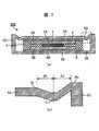
- FIG. 5A is a cross-sectional view of a power semiconductor module 300 according to another embodiment
- FIG. 5B is an enlarged view of a dotted line encircled portion in FIG.
- the convex portion of the intermediate member 5D is formed so that the distance 5J is larger than the distance 5K.
- FIG. 6 is a view showing the relationship between the distance from the center position in the width direction of the intermediate member 5D to the convex vertex 7 and the stress of the side wall 5C generated in the third step shown in FIG.
- FIG. 6 shows the distance from the center position of the intermediate member 5D in the width direction (between the first connection portion 5H and the second connection portion 5I) to the convex vertex portion 7, and the third assembly step. It is the figure which showed the relationship of the stress of the joining member 6 after completion
- the vertical axis, horizontal axis, and analysis method in FIG. 6 are the same as those in FIG.
- produces in the side wall 5C at a 3rd process becomes small, so that the convex vertex part 7 is formed in the side close
- FIG. 7A is a cross-sectional view of a power semiconductor module 300 according to another embodiment
- FIG. 7B is an enlarged view of a dotted line encircled portion in FIG. 7A.
- the convex vertex 7 is formed at the center of the intermediate member 5D, and the distance 5J and the distance 5K are equal. Thereby, it is possible to reduce both the stress of the joining member 6 and the stress of the side wall 5 ⁇ / b> C generated after the completion of the third assembly process in a balanced manner.
- each embodiment shown by FIG.3, FIG5 and FIG.7 suppresses the damage of the power semiconductor module 300 by selecting suitably according to the location which should reduce stress, and the shape of case 5.
- FIG. 8 shows the arrangement of the convex deformation region 5F in the intermediate member 5D of the case 5 in order to reduce the residual stress to the joining member 6.
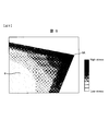
- FIG. 9 is a diagram showing a result of finite element analysis simulating the tensile stress of the joining member 6 after the second assembly process.
- the maximum tensile stress generated in the joining member 6 occurs in the corner portion 6 ⁇ / b> A of the joining member 6 after the end of the second assembly process. Further, when looking at the distribution of the tensile stress in the surface of the joining member 6, a large tensile force is distributed at the end portion, that is, closer to the side of the joining member 6 than the central portion of the surface of the joining member 6. I understand that. Further, when looking at the distribution of the tensile stress on the side of the joining member 6, it can be seen that a greater tensile force is generated in a place closer to the corner 6 ⁇ / b> A of the joining member 6.
- the convex deformation region 5F is formed so as to surround the first heat radiating member 5A facing the joining member 6.
- the convex deformation region 5F surrounds the vicinity of the side portion of the joining member 6 where a relatively high tensile stress is generated, so that the effect of reducing the residual stress can be maximized.
- the corner of the first heat radiating member 5A is defined as a corner 9A
- the corner of the case 5 is defined as a corner 9B
- the convex deformation region 5F is formed so as to overlap a line segment connecting the corner portion 9A and the corner portion 9B. That is, when projected from the direction perpendicular to the heat radiating surface of the first heat radiating member 5A, the projected portion of the convex deformation region 5F overlaps the line segment connecting the corner 9A and the corner 9B.
- the corner portion 9A of the first heat radiating member 5A and the corner portion 6A of the joining member 6 overlap or are close to each other. Will be placed in position. Thereby, the residual stress reduction effect can be obtained while minimizing the deformation of the intermediate member 5D in the region of the corner 6A of the joining member 6 having a large tensile stress illustrated in FIG. Therefore, distortion and destruction of the case 5 can be suppressed.
- the corner portion 9B can also be said to be a corner portion of the intermediate member 5D.
- the convex deformation region 5F is formed to have a substantially L shape around the corner portion 9A of the first heat radiating member 5A.
- the projected portion of the convex deformation region 5F is the two adjacent sides of the first heat dissipation member 5A for forming the corner portion 9A of the first heat dissipation member 5A. It has a shape that bends along.
- the shape of the first heat radiating member 5A is substantially the same as or similar to the shape of the joining member 6.
- the corner portion 9A of the first heat radiating member 5A and the joining member 6 overlaps or is disposed at a position close to the corner 6A. Thereby, it is possible to balance the deformation amount of the intermediate member 5D and the residual stress reduction effect.
- FIG. 10 is a cross-sectional view of a power semiconductor module according to the second embodiment of the present invention.
- the intermediate member 5E facing the intermediate member 5D is also curved so as to be convex toward the storage space of the case 5 similarly to the intermediate member 5D. Is forming.
- the force which presses the 1st heat radiating member 5A by intermediate member 5D to the circuit body 100 side the force which presses the 2nd heat radiating member 5B by the intermediate member 5E to the circuit body 100 side generate
- the convex portion described in the first embodiment is formed on both the intermediate member 5D and the intermediate member 5E, the residual stress of the joining member 6 can be reduced.
- the same effects as those of the first embodiment can be obtained by appropriately combining the formation positions and formation regions of the convex portions explained in FIGS. 3, 5, 7, and 8.
- FIG. 11 is a cross-sectional view of a power semiconductor module according to the third embodiment of the present invention.
- the intermediate member 5D is formed thinner than the first heat radiating member 5A.
- the reaction force of the intermediate member 5D in the second assembly step (FIG. 2B) can be reduced, and the workability in the third assembly step (FIG. 2D) can be improved. It is.
- the first heat radiating member 5A and the circuit body 100 are in close contact with each other via the joining member 6. If a load that deforms the intermediate member 5D is applied in this state, about half of the load is reduced.
- the effect similar to the above can be acquired by making thickness in the intermediate member 5E side demonstrated in FIG. 10 smaller than 5 A of 1st heat radiating members.
- FIG. 12 is a diagram showing an assembly process of the power semiconductor module 300 according to the fourth embodiment of the present invention.
- the power semiconductor module 300 of the present embodiment is different in that a high temperature heat treatment shown in FIG. 12D is performed simultaneously with or after the third assembly process shown in FIG.
- a high temperature heat treatment shown in FIG. 12D is performed simultaneously with or after the third assembly process shown in FIG.
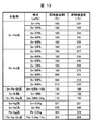
- FIG. 13 is a diagram showing the melting point of a general solder material.
- the melting point of general solder materials is 135 ° C. or higher. Therefore, it is necessary to perform heat treatment at 135 ° C. or higher in order to melt and connect them once and to develop a connection holding force. There is.
- a general power semiconductor module is used at the manufacturing stage because the crosslinking reaction proceeds in the material at high temperatures.
- heat treatment is performed at 120 ° C. or higher, which is the use temperature range, to make it difficult for the material to change in the use environment. Therefore, in the third step, when the bonding member 6 is heat-treated at a high temperature, it is necessary to be 120 ° C. or higher.
- FIG. 14 shows the amount of return of the storage member 5 (spring back amount) and the temperature at that time when a member simulating the circuit body 100 is inserted into the case 5 and subjected to pressing deformation and then the pressing is released. It is the figure which showed the relationship. It can be seen that the return amount of the case 5 is reduced by raising the temperature. From this result, it can be seen that in order to reduce the reaction force against the deformation of the metal case 5, it is preferable that the temperature of the high temperature treatment is high.
- the metal case 5 and the circuit body 100 in a deformed state are simultaneously subjected to a high temperature treatment to cause the joining member 6 to exhibit a connection holding force, and against the pressing deformation of the intermediate member 5D of the metal case 5.
- the high-temperature treatment temperature needs to be 120 ° C. or higher in order to reduce the reaction force.
- the power conversion device according to the embodiment of the present invention can be applied to a hybrid vehicle or a pure electric vehicle.
- the power conversion device according to the embodiment of the present invention is applied to a hybrid vehicle.
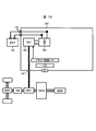
- the control configuration and the circuit configuration of the power converter will be described with reference to FIGS. 15 and 16.
- FIG. 15 is a diagram showing a control block of a hybrid vehicle (hereinafter referred to as “HEV”).
- HEV hybrid vehicle
- Engine EGN and motor generator MG1 generate vehicle running torque.
- Motor generator MG1 not only generates rotational torque but also has a function of converting mechanical energy applied from the outside to motor generator MG1 into electric power.
- the motor generator MG1 is, for example, a synchronous machine or an induction machine, and operates as a motor or a generator depending on the operation method as described above.
- motor generator MG1 When motor generator MG1 is mounted on an automobile, it is desirable to obtain a small and high output, and a permanent magnet type synchronous motor using a magnet such as neodymium is suitable. Further, the permanent magnet type synchronous motor generates less heat from the rotor than the induction motor, and is excellent for automobiles from this viewpoint.
- the output torque on the output side of the engine EGN is transmitted to the motor generator MG1 via the power distribution mechanism TSM, and the rotation torque from the power distribution mechanism TSM or the rotation torque generated by the motor generator MG1 is transmitted via the transmission TM and the differential gear DEF. Transmitted to the wheels.
- rotational torque is transmitted from the wheels to motor generator MG1, and AC power is generated based on the supplied rotational torque.
- the generated AC power is converted to DC power by the power conversion device 200 as described later, and the high-voltage battery 136 is charged, and the charged power is used again as travel energy.
- the inverter circuit 140 is electrically connected to the battery 136 via the DC connector 138, and power is exchanged between the battery 136 and the inverter circuit 140.
- motor generator MG1 When motor generator MG1 is operated as a motor, inverter circuit 140 generates AC power based on DC power supplied from battery 136 via DC connector 138 and supplies it to motor generator MG1 via AC terminal 188.
- the configuration comprising motor generator MG1 and inverter circuit 140 operates as a first motor generator unit.
- the vehicle can be driven only by the power of the motor generator MG1 by operating the first motor generator unit as an electric unit by the electric power of the battery 136. Further, in the present embodiment, the battery 136 can be charged by operating the first motor generator unit as a power generation unit by the power of the engine 120 or the power from the wheels to generate power.
- the battery 136 is also used as a power source for driving an auxiliary motor.
- the auxiliary motor is, for example, a motor for driving a compressor of an air conditioner or a motor for driving a control hydraulic pump.
- DC power is supplied from the battery 136 to the power semiconductor module for auxiliary machinery, and the power semiconductor module for auxiliary machinery generates AC power and supplies it to the motor for auxiliary machinery.
- the auxiliary power semiconductor module has basically the same circuit configuration and function as the inverter circuit 140, and controls the phase, frequency, and power of alternating current supplied to the auxiliary motor.
- the power conversion device 200 includes a capacitor module 500 for smoothing the DC power supplied to the inverter circuit 140.
- the power conversion device 200 includes a communication connector 21 for receiving a command from a host control device or transmitting data representing a state to the host control device.
- Power conversion device 200 calculates a control amount of motor generator MG1 by control circuit 172 based on a command input from connector 21, further calculates whether to operate as a motor or a generator, and based on the calculation result.
- the control pulse is generated, and the control pulse is supplied to the driver circuit 174.
- the driver circuit 174 generates a driving pulse for controlling the inverter circuit 140 based on the supplied control pulse.
- an insulated gate bipolar transistor is used as a semiconductor element, and hereinafter abbreviated as IGBT.
- the IGBT 328 and the diode 156 that operate as the upper arm, and the IGBT 330 and the diode 166 that operate as the lower arm constitute the series circuit 150 of the upper and lower arms.
- the inverter circuit 140 includes the series circuit 150 corresponding to three phases of the U phase, the V phase, and the W phase of the AC power to be output.
- the series circuit 150 of the upper and lower arms of each of the three phases outputs an alternating current from the intermediate electrode 169 that is the midpoint portion of the series circuit.
- This intermediate electrode 169 is connected to AC bus bars 802 and 804 described below which are AC power lines to motor generator MG1 through AC terminal 159 and AC terminal 188.
- the collector electrode 153 of the IGBT 328 of the upper arm is electrically connected to the capacitor terminal 506 on the positive electrode side of the capacitor module 500 via the positive electrode terminal 157.
- the emitter electrode of the IGBT 330 of the lower arm is electrically connected to the capacitor terminal 504 on the negative electrode side of the capacitor module 500 via the negative electrode terminal 158.
- control circuit 172 receives a control command from the host control device via the connector 21, and based on this, the IGBT 328 that configures the upper arm or the lower arm of each phase series circuit 150 that constitutes the inverter circuit 140. And a control pulse that is a control signal for controlling the IGBT 330 is generated and supplied to the driver circuit 174.
- the driver circuit 174 supplies a drive pulse for controlling the IGBT 328 and IGBT 330 constituting the upper arm or lower arm of each phase series circuit 150 to the IGBT 328 and IGBT 330 of each phase based on the control pulse.
- IGBT 328 and IGBT 330 perform conduction or cutoff operation based on the drive pulse from driver circuit 174, convert DC power supplied from battery 136 into three-phase AC power, and supply the converted power to motor generator MG1. Is done.
- the IGBT 328 includes a collector electrode 153, a signal emitter electrode 155, and a gate electrode 154.
- the IGBT 330 includes a collector electrode 163, a signal emitter electrode 165, and a gate electrode 164.
- a diode 156 is electrically connected between the collector electrode 153 and the emitter electrode 155.
- a diode 166 is electrically connected between the collector electrode 163 and the emitter electrode 165.
- MOSFET metal oxide semiconductor field effect transistor
- IGBT is suitable when the DC voltage is relatively high
- MOSFET is suitable when the DC voltage is relatively low.
- the capacitor module 500 includes a positive capacitor terminal 506, a negative capacitor terminal 504, a positive power terminal 509, and a negative power terminal 508.
- the high-voltage DC power from the battery 136 is supplied to the positive-side power terminal 509 and the negative-side power terminal 508 via the DC connector 138, and the positive-side capacitor terminal 506 and the negative-side capacitor of the capacitor module 500.
- the voltage is supplied from the terminal 504 to the inverter circuit 140.
- the DC power converted from the AC power by the inverter circuit 140 is supplied to the capacitor module 500 from the positive capacitor terminal 506 and the negative capacitor terminal 504, and is connected to the positive power terminal 509 and the negative power terminal 508. Is supplied to the battery 136 via the DC connector 138 and accumulated in the battery 136.
- the control circuit 172 includes a microcomputer (hereinafter referred to as “microcomputer”) for performing arithmetic processing on the switching timing of the IGBT 328 and the IGBT 330.
- the input information to the microcomputer includes a target torque value required for the motor generator MG1, a current value supplied from the series circuit 150 to the motor generator MG1, and a magnetic pole position of the rotor of the motor generator MG1.
- the target torque value is based on a command signal output from a host controller (not shown).
- the current value is detected based on a detection signal from the current sensor 180.
- the magnetic pole position is detected based on a detection signal output from a rotating magnetic pole sensor (not shown) such as a resolver provided in the motor generator MG1.
- the current sensor 180 detects the current value of three phases, but the current value for two phases may be detected and the current for three phases may be obtained by calculation. .
- the microcomputer in the control circuit 172 calculates the d-axis and q-axis current command values of the motor generator MG1 based on the target torque value, the calculated d-axis and q-axis current command values, and the detected d
- the voltage command values for the d-axis and q-axis are calculated based on the difference between the current values for the axes and q-axis, and the calculated voltage command values for the d-axis and q-axis are calculated based on the detected magnetic pole position. Convert to phase, V phase, and W phase voltage command values.
- the microcomputer generates a pulse-like modulated wave based on the comparison between the fundamental wave (sine wave) and the carrier wave (triangular wave) based on the voltage command values of the U-phase, V-phase, and W-phase, and the generated modulation
- the wave is output to the driver circuit 174 as a PWM (pulse width modulation) signal.
- the driver circuit 174 When driving the lower arm, the driver circuit 174 outputs a drive signal obtained by amplifying the PWM signal to the gate electrode of the corresponding IGBT 330 of the lower arm. Further, when driving the upper arm, the driver circuit 174 amplifies the PWM signal after shifting the level of the reference potential of the PWM signal to the level of the reference potential of the upper arm, and uses this as a drive signal as a corresponding upper arm. Are output to the gate electrodes of the IGBTs 328 respectively.
- the microcomputer in the control circuit 172 detects abnormality (overcurrent, overvoltage, overtemperature, etc.) and protects the series circuit 150. For this reason, sensing information is input to the control circuit 172. For example, information on the current flowing through the emitter electrodes of the IGBTs 328 and IGBTs 330 is input to the corresponding drive units (ICs) from the signal emitter electrode 155 and the signal emitter electrode 165 of each arm. Thereby, each drive part (IC) detects an overcurrent, and when an overcurrent is detected, the switching operation of the corresponding IGBT 328 and IGBT 330 is stopped, and the corresponding IGBT 328 and IGBT 330 are protected from the overcurrent.
- ICs drive units
- Information on the temperature of the series circuit 150 is input to the microcomputer from a temperature sensor (not shown) provided in the series circuit 150.
- voltage information on the DC positive side of the series circuit 150 is input to the microcomputer.
- the microcomputer performs over-temperature detection and over-voltage detection based on the information, and stops switching operations of all the IGBTs 328 and IGBTs 330 when an over-temperature or over-voltage is detected.
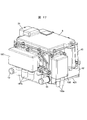
- FIG. 17 and 18 are external perspective views of the power conversion device 200 according to the embodiment of the present invention.
- FIG. 18 shows a state in which the AC connector 187 and the DC connector 138 are removed.
- the power conversion device 200 according to the present embodiment has an effect that the planar shape is a rectangular parallelepiped shape, which can be reduced in size and can be easily attached to the vehicle.
- 8 is a lid
- 10 is a housing
- 12 is a flow path forming body
- 13 is a cooling medium inlet pipe
- 14 is an outlet pipe
- 420 is a lower cover.
- the connector 21 is a signal connector provided for connection to the outside.
- the lid 8 is fixed to the upper opening of the housing 10 in which circuit components constituting the power conversion device 200 are accommodated.
- the flow path forming body 12 fixed to the lower portion of the housing 10 holds a power semiconductor module 300 and a capacitor module 500, which will be described later, and cools them with a cooling medium.
- a cooling medium For example, water is often used as the cooling medium, and will be described below as a refrigerant.
- the inlet pipe 13 and the outlet pipe 14 are provided on one side surface of the flow path forming body 12, and the refrigerant supplied from the inlet pipe 13 flows into a flow path 19 described later in the flow path forming body 12 and is discharged from the outlet pipe 14. Is done.
- the AC interface 185 to which the AC connector 187 is attached and the DC interface 137 to which the DC connector 138 is attached are provided on the side surface of the housing 10.
- the AC interface 185 is provided on the side surface where the pipes 13 and 14 are provided, and the AC wiring 187 a of the AC connector 187 attached to the AC interface 185 extends downward between the pipes 13 and 14.
- the DC interface 137 is provided on a side surface adjacent to the side surface on which the AC interface 185 is provided, and the DC wiring 135J of the DC connector 138 attached to the DC interface 137 also extends below the power conversion device 200.
- FIG. 19 is a diagram showing a state where lid 8, DC interface 137, and AC interface 185 are removed from power conversion device 200 shown in FIG.
- An opening 10a to which the AC interface 185 is fixed is formed on one side of the housing 10, and an opening 10b to which the DC interface 137 is fixed is formed on the other adjacent side.
- 20 is a view showing a state where the housing 10 is removed from the flow path forming body 12 in FIG.
- the housing 10 has two storage spaces, and is divided into an upper storage space and a lower storage space by a partition wall 10c.
- the control circuit board 20 to which the connector 21 is fixed is stored in the upper storage space, and the driver circuit board 22 and a bus bar assembly 800 described later are stored in the lower storage space.
- a control circuit 172 shown in FIG. 16 is mounted on the control circuit board 20, and a driver circuit board 174 is mounted on the driver circuit board 22.
- the control circuit board 20 and the driver circuit board 22 are connected by a flat cable (not shown) (see FIG. 21 described later).
- the flat cable passes through a slit-shaped opening 10d formed in the partition wall 10c and is stored in the lower storage space.
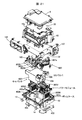
- FIG. 21 is an exploded perspective view of the power converter 200.
- control circuit board 20 on which the control circuit 172 is mounted is disposed inside the lid 8, that is, in the upper storage space of the housing 10.
- the lid 8 is formed with an opening 5J for the connector 21.
- Low voltage DC power for operating the control circuit in the power converter 200 is supplied from the connector 21.
- the flow path forming body 12 is formed with a flow path through which the refrigerant flowing from the inlet pipe 13 flows.
- the flow path forms a U-shaped flow path that flows along the three side surfaces of the flow path forming body 12.
- the refrigerant that has flowed from the inlet pipe 13 flows into the flow path from one end of the U-shaped flow path, flows through the flow path, and then flows out from the outlet pipe 14 connected to the other end of the flow path.
- Three openings 402a to 402c are formed on the upper surface of the flow path, and the power semiconductor modules 300U, 300V, and 300W incorporating the series circuit 150 (see FIG. 15) are connected to the inside of the flow path from the openings 402a to 402c. Inserted into.
- the power semiconductor module 300U includes a U-phase series circuit 150
- the power semiconductor module 300V includes a V-phase series circuit 150
- the power semiconductor module 300W includes a W-phase series circuit 150.
- These power semiconductor modules 300U to 300W have the same configuration and the same external shape.
- the openings 402a to 402c are closed by the flange portions of the inserted power semiconductor modules 300U to 300W.
- a storage space 405 for storing electrical components is formed in the flow path forming body 12 so as to be surrounded by the U-shaped flow path.
- the capacitor module 500 is stored in the storage space 405.
- the capacitor module 500 stored in the storage space 405 is cooled by the refrigerant flowing in the flow path.
- a bus bar assembly 800 to which AC bus bars 802U to 802W are attached is disposed above the capacitor module 500.
- the bus bar assembly 800 is fixed to the upper surface of the flow path forming body 12.
- a current sensor 180 is fixed to the bus bar assembly 800.
- the driver circuit board 22 is disposed above the bus bar assembly 800 by being fixed to a support member 807a provided in the bus bar assembly 800. As described above, the control circuit board 20 and the driver circuit board 22 are connected by the flat cable 23. The flat cable 23 is pulled out from the lower storage space to the upper storage space through the slit-shaped opening 10d formed in the partition wall 10c.
- the power semiconductor modules 300U to 300W, the driver circuit board 22 and the control circuit board 20 are hierarchically arranged in the height direction, and the control circuit board 20 is farthest from the high-power system power semiconductor modules 300U to 300W. Therefore, it is possible to reduce mixing of switching noise and the like on the control circuit board 20 side. Furthermore, since the driver circuit board 22 and the control circuit board 20 are arranged in different storage spaces partitioned by the partition wall 10c, the partition wall 10c functions as an electromagnetic shield and enters the control circuit board 20 from the driver circuit board 22. Noise can be reduced.
- the housing 10 is made of a metal material such as aluminum.
- control circuit board 20 is fixed to the partition wall 10c formed integrally with the housing 10, the mechanical resonance frequency of the control circuit board 20 is increased against external vibration. Therefore, it is difficult to be affected by vibration from the vehicle side, and reliability is improved.
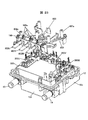
- FIG. 22 is an external perspective view in which the power semiconductor modules 300U to 300W, the capacitor module 500, and the bus bar assembly 800 are assembled to the flow path forming body 12.
- FIG. 23 shows a state where the bus bar assembly 800 is removed from the flow path forming body 12. The bus bar assembly 800 is bolted to the flow path forming body 12.
- FIGS. 24 is a perspective view of the flow path forming body 12
- FIG. 25 is an exploded perspective view of the flow path forming body 12 as seen from the back side.
- the flow path forming body 12 is a rectangular parallelepiped having a planar shape, and an inlet pipe 13 and an outlet pipe 14 are provided on a side surface 12d thereof.
- the side surface 12d is formed in a stepped portion where the pipes 13 and 14 are provided.
- the flow path 19 is formed in a U shape so as to follow the remaining three side faces 12a to 12c.
- a U-shaped opening 404 connected to one having the same shape as the cross-sectional shape of the flow path 19 is formed on the back surface side of the flow path forming body 12.
- the opening 404 is closed by a U-shaped lower cover 420.
- a seal member 409a is provided between the lower cover 420 and the flow path forming body 12, and airtightness is maintained.
- the U-shaped channel 19 is divided into three channel sections 19a, 19b, and 19c according to the direction in which the refrigerant flows.
- the first flow path section 19a is provided along the side face 12a at a position facing the side face 12d provided with the pipes 13 and 14, and the second flow path section 19b is one of the side faces 12a.
- the third flow path section 19c is provided along the side surface 12c adjacent to the other side of the side surface 12a.
- the refrigerant flows from the inlet pipe 13 into the flow path section 19b, flows in the order of the flow path section 19b, the flow path section 19a, and the flow path section 19c as shown by the broken line arrows, and flows out from the outlet pipe 14.
- a rectangular opening 402a parallel to the side surface 12a is formed at a position facing the flow path section 19a, and at a position facing the flow path section 19b.
- a rectangular opening 402b parallel to the side surface 12b is formed, and a rectangular opening 402c parallel to the side surface 12c is formed at a position facing the flow path section 19c.
- the power semiconductor modules 300U to 300W are inserted into the flow path 19 through these openings 402a to 402c.
- the lower cover 420 is formed with a convex portion 406 that protrudes toward the lower side of the flow path 19 at a position facing the above-described openings 402a to 402c.
- These convex portions 406 are dents when viewed from the flow path 19 side, and the lower end portions of the power semiconductor modules 300U to 300W inserted from the openings 402a to 402c enter these dents. Since the flow path forming body 12 is formed so that the opening 404 and the openings 402a to 402c face each other, the flow path forming body 12 is configured to be easily manufactured by aluminum casting.
- the flow path forming body 12 is provided with a rectangular storage space 405 formed so that three sides are surrounded by the flow path 19.
- the capacitor module 500 is stored in the storage space 405. Since the storage space 405 surrounded by the flow path 19 has a rectangular parallelepiped shape, the capacitor module 500 can be formed into a rectangular parallelepiped shape, and the productivity of the capacitor module 500 is improved.
- the power semiconductor modules 300U to 300W and the power semiconductor modules 301a to 301c used in the inverter circuit 140 and the inverter circuit 142 will be described with reference to FIGS.
- the power semiconductor modules 300U to 300W and the power semiconductor modules 301a to 301c all have the same structure, and the structure of the power semiconductor module 300U will be described as a representative.
- the signal terminal 325U corresponds to the gate electrode 154 and the signal emitter electrode 155 disclosed in FIG. 2
- the signal terminal 325L corresponds to the gate electrode 164 and the emitter electrode 165 disclosed in FIG. To do.
- the DC positive terminal 315B is the same as the positive terminal 157 disclosed in FIG.
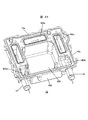
- FIG. 26A is a perspective view of the power semiconductor module 300U of the present embodiment.
- FIG. 26B is a cross-sectional view of the power semiconductor module 300 ⁇ / b> U of the present embodiment cut along a cross section D and viewed from the direction E.
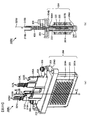
- FIG. 27 is a diagram showing a power semiconductor module 300U in which the screw 309 and the second sealing resin 351 are removed from the state shown in FIG. 26 to facilitate understanding.
- FIG. 27A is a perspective view
- FIG. 27B is a cross-sectional view taken along the section D and viewed from the direction E similarly to FIG.
- FIG. 27C shows a cross-sectional view before the fin 305 is pressed and the bending portion 304A is deformed.
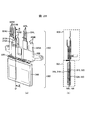
- FIG. 28 is a diagram showing a power semiconductor module 300U in which the module case 304 is further removed from the state shown in FIG.
- FIG. 28A is a perspective view
- FIG. 28B is a cross-sectional view taken along the section D and viewed from the direction E as in FIGS. 26B and 27B.
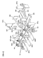
- FIG. 29 is a perspective view of the power semiconductor module 300U from which the first sealing resin 348 and the wiring insulating portion 608 are further removed from the state shown in FIG.
- FIG. 30 is a diagram for explaining an assembly process of the module primary sealing body 302.
- the power semiconductor elements (IGBT 328, IGBT 330, diode 156, and diode 166) constituting the upper and lower arm series circuit 150, as shown in FIGS. 28 and 29, are formed by the conductor plate 315 and the conductor plate 318, or the conductor plate 320 and the conductor plate. By 319, it is fixed by being sandwiched from both sides.
- the conductor plate 315 and the like are sealed with the first sealing resin 348 with the heat dissipation surface exposed, and the insulating sheet 333 is thermocompression bonded to the heat dissipation surface.
- the first sealing resin 348 has a polyhedral shape (here, a substantially rectangular parallelepiped shape).
- the module primary sealing body 302 sealed with the first sealing resin 348 is inserted into the module case 304 and sandwiched with the insulating sheet 333, and is thermocompression bonded to the inner surface of the module case 304 that is a CAN type cooler.
- the CAN-type cooler is a cylindrical cooler having an insertion port 306 on one surface and a bottom on the other surface.
- the gap remaining inside the module case 304 is filled with the second sealing resin 351.
- case 5 described in the first to fourth embodiments corresponds to the module case 304 in the present embodiment.
- circuit body 100 described in the first to fourth embodiments corresponds to the module primary sealing body 302 in the present embodiment.
- the module case 304 is made of a member having electrical conductivity, for example, an aluminum alloy material (Al, AlSi, AlSiC, Al—C, etc.), and is integrally formed without a joint.
- the module case 304 has a structure in which no opening other than the insertion port 306 is provided.
- the insertion port 306 is surrounded by a flange 304B. Further, as shown in FIG. 26 (a), the first heat radiating surface 307A and the second heat radiating surface 307B, which are wider than the other surfaces, are arranged facing each other so as to face these heat radiating surfaces.
- Each power semiconductor element (IGBT 328, IGBT 330, diode 156, diode 166) is arranged.
- the three surfaces that connect the first heat radiation surface 307A and the second heat radiation surface 307B that face each other constitute a surface that is sealed with a narrower width than the first heat radiation surface 307A and the second heat radiation surface 307B, and the other one side surface
- An insertion slot 306 is formed in
- the shape of the module case 304 does not have to be an accurate rectangular parallelepiped, and the corners may be curved as shown in FIG.
- the metal case having such a shape By using the metal case having such a shape, even when the module case 304 is inserted into the flow path 19 through which a coolant such as water or oil flows, a seal against the coolant can be secured by the flange 304B. Can be prevented from entering the inside of the module case 304 with a simple configuration.
- the fins 305 are uniformly formed on the first heat radiation surface 307A and the second heat radiation surface 307B facing each other.
- a curved portion 304A having an extremely thin thickness is formed on the outer periphery of the first heat radiating surface 307A and the second heat radiating surface 307B. Since the curved portion 304A is extremely thin to such an extent that it can be easily deformed by pressurizing the fin 305, the productivity after the module primary sealing body 302 is inserted is improved.
- the insulating sheet 333 peels from the module primary sealing body 302 or the module case 304 by forming the convex deformation area
- the module case is reduced by reducing the thermal resistance of the heat transfer path from the power semiconductor element to the outer surface of the module case 304. Heat dissipation from the outer surface of 304 is promoted. As a result, the current flowing through the power semiconductor element can be increased and the cooling unit of the power conversion device can be reduced in size, and the amount of output current per volume of the power conversion device can be greatly increased.
- the gap between the conductor plate 315 and the inner wall of the module case 304 can be reduced by thermocompression bonding the conductor plate 315 and the like to the inner wall of the module case 304 via the insulating sheet 333, and the power semiconductor The generated heat of the element can be efficiently transmitted to the fin 305. Further, by providing the insulating sheet 333 with a certain degree of thickness and flexibility, the generation of thermal stress can be absorbed by the insulating sheet 333, which is favorable for use in a power conversion device for a vehicle having a large temperature change. .
- a metallic DC positive wiring 315A and a DC negative wiring 319A for electrical connection with the capacitor module 500 are provided, and a DC positive terminal 315B (157) and a DC are connected to the tip thereof. Negative terminals 319B (158) are formed respectively.
- metallic AC wiring 320A for supplying AC power to motor generator MG1 is provided, and AC terminal 320B (159) is formed at the tip thereof.
- the DC positive electrode wiring 315A is connected to the conductor plate 315
- the DC negative electrode wiring 319A is connected to the conductor plate 319
- the AC wiring 320A is connected to the conductor plate 320.
- metal signal wirings 324U and 324L for electrical connection with the driver circuit 174 are provided, and the signal terminals 325U (154, 155) and the signal terminals 325L are provided at the front ends thereof. (164, 165) are formed.
- the signal wiring 324U is connected to the IGBT 328, and the signal wiring 324L is connected to the IGBT 328.
- the DC positive wiring 315A, the DC negative wiring 319A, the AC wiring 320A, the signal wiring 324U, and the signal wiring 324L are integrally molded as the auxiliary mold body 600 in a state where they are insulated from each other by the wiring insulating portion 608 formed of a resin material. Is done.
- the wiring insulating portion 608 also acts as a support member for supporting each wiring, and a thermosetting resin or a thermoplastic resin having an insulating property is suitable for the resin material used therefor. As a result, it is possible to secure insulation between the DC positive electrode wiring 315A, the DC negative electrode wiring 319A, the AC wiring 320A, the signal wiring 324U, and the signal wiring 324L, thereby enabling high-density wiring.
- the auxiliary mold body 600 is fixed to the module case 304 with a screw 309 that passes through a screw hole provided in the wiring insulating portion 608 after being metal-bonded to the module primary sealing body 302 at the connection portion 370.
- TIG welding or the like can be used for metal bonding between the module primary sealing body 302 and the auxiliary mold body 600 in the connection portion 370.
- the direct current positive electrode wiring 315A and the direct current negative electrode wiring 319A are stacked on each other in a state of facing each other with the wiring insulating portion 608 interposed therebetween, and have a shape extending substantially in parallel. With such an arrangement and shape, the current that instantaneously flows during the switching operation of the power semiconductor element flows oppositely and in the opposite direction. As a result, the magnetic fields produced by the currents cancel each other out, and this action can reduce the inductance.
- the AC wiring 320A and the signal terminals 325U and 325L also extend in the same direction as the DC positive wiring 315A and the DC negative wiring 319A.
- connection portion 370 in which the module primary sealing body 302 and the auxiliary mold body 600 are connected by metal bonding is sealed in the module case 304 by the second sealing resin 351.
- the auxiliary module side DC positive connection terminal 315C, the auxiliary module side DC negative connection terminal 319C, the auxiliary module side AC connection terminal 320C, and the auxiliary module side signal connection are provided on the auxiliary module 600 side of the connecting portion 370.
- Terminals 326U and auxiliary module side signal connection terminals 326L are arranged in a line.
- the element side DC positive connection terminal 315D, the element side DC negative connection terminal 319D, The element side AC connection terminal 320D, the element side signal connection terminal 327U, and the element side signal connection terminal 327L are arranged in a line.
- the structure in which the terminals are arranged in a row in the connection portion 370 facilitates the manufacture of the module primary sealing body 302 by transfer molding.
- a terminal constituted by DC positive electrode wiring 315A (including DC positive electrode terminal 315B and auxiliary module side DC positive electrode connection terminal 315C) and element side DC positive electrode connection terminal 315D is referred to as a positive electrode side terminal.
- a terminal constituted by the DC negative electrode wiring 319A (including the DC negative electrode terminal 319B and the auxiliary module side DC negative electrode connection terminal 319C) and the element side DC negative electrode connection terminal 315D is referred to as a negative electrode side terminal.
- a terminal constituted by the AC wiring 320A (including the AC terminal 320B and the auxiliary module side AC connection terminal 320C) and the element side AC connection terminal 320D is referred to as an output terminal.
- a terminal constituted by the signal wiring 324U (including the signal terminal 325U and the auxiliary module side signal connection terminal 326U) and the element side signal connection terminal 327U is referred to as an upper arm signal terminal.
- a terminal constituted by the signal wiring 324L (including the signal terminal 325L and the auxiliary module side signal connection terminal 326L) and the element side signal connection terminal 327L is referred to as a lower arm signal terminal.
- Each of the above terminals protrudes from the first sealing resin 348 and the second sealing resin 351 through the connection portion 370.
- Each protruding portion from the first sealing resin 348 (element side DC positive connection terminal 315D, element side DC negative connection terminal 319D, element side AC connection terminal 320D, element side signal connection terminal 327U, and element side signal connection terminal 327L) are arranged in a line along one surface of the first sealing resin 348 having a polyhedral shape as described above. Further, the positive electrode side terminal and the negative electrode side terminal protrude in a stacked state from the second sealing resin 351 and extend outside the module case 304.
- the power semiconductor element and the terminal are connected during mold clamping when the module primary sealing body 302 is manufactured by sealing the power semiconductor element with the first sealing resin 348. It is possible to prevent an excessive stress on the part and a gap in the mold from occurring. Further, since the magnetic fluxes in the directions canceling each other are generated by the currents in the opposite directions flowing through each of the stacked positive electrode side terminals and negative electrode side terminals, the inductance can be reduced.
- the auxiliary module side DC positive electrode connection terminal 315C and the auxiliary module side DC negative electrode connection terminal 319C are the DC positive electrode terminal 315B and the tip of the DC positive electrode wiring 315A and the DC negative electrode wiring 319A opposite to the DC negative electrode terminal 319B. It is formed in each part. Further, the auxiliary module side AC connection terminal 320C is formed at the tip of the AC wiring 320A opposite to the AC terminal 320B. The auxiliary module side signal connection terminals 326U and 326L are formed at the distal ends of the signal wirings 324U and 324L opposite to the signal terminals 325U and 325L, respectively.
- FIG. 31 is an external perspective view of the capacitor module 500.
- a plurality of capacitor cells are provided in the capacitor module 500.
- Capacitor terminals 503a to 503c are provided on the upper surface of the capacitor module 500 so as to protrude close to the surface of the capacitor module 500 facing the flow path 19.
- the capacitor terminals 503a to 503c are formed corresponding to the positive terminal 157 and the negative terminal 158 of each power semiconductor module 300.
- the capacitor terminals 503a to 503c have the same shape, and an insulating sheet is provided between the negative electrode side capacitor terminal 504 and the positive electrode side capacitor terminal 506 constituting the capacitor terminals 503a to 503c, and insulation between the terminals is ensured. Yes.
- Projections 500e and 500f are formed on the upper portion of the capacitor module 500 on the side surface 500d.
- a discharge resistor is mounted in the protruding portion 500e, and a Y capacitor for countering common mode noise is mounted in the protruding portion 500f.
- the power supply terminals 508 and 509 shown in FIG. 5 are attached to the terminals 500g and 500h protruding from the upper surface of the protruding portion 500f.
- recesses 405a and 405b are formed between the openings 402b and 402c and the side surface 12d.
- the discharge resistor mounted in the protruding portion 500e is a resistor for discharging the electric charge accumulated in the capacitor cell in the capacitor module 500 when the inverter is stopped. Since the recessed portion 405a in which the protruding portion 500e is accommodated is provided immediately above the flow path of the refrigerant flowing in from the inlet pipe 13, it is possible to suppress the temperature rise of the discharge resistance during discharge.
- FIG. 32 is a perspective view of the bus bar assembly 800.
- Bus bar assembly 800 detects U, V, and W phase AC bus bars 802U, 802V, and 802W, a holding member 803 for holding and fixing AC bus bars 802U to 802W, and an AC current flowing through AC bus bars 802U to 802W.
- AC bus bars 802U to 802W are each formed of a wide conductor.
- a plurality of support members 807 a for holding the driver circuit board 22 are formed on the holding member 803 made of an insulating material such as resin so as to protrude upward from the holding member 803.
- the current sensor 180 is parallel to the side face 12d at a position close to the side face 12d of the flow path forming body 12.
- the current sensor 180 Located in the assembly 800.
- through-holes 181 for penetrating the AC bus bars 802U to 802W are formed.
- a sensor element is provided in a portion where the through hole 181 of the current sensor 180 is formed, and a signal line 182 a of each sensor element protrudes from the upper surface of the current sensor 180.
- Each sensor element is arranged side by side in the extending direction of the current sensor 180, that is, in the extending direction of the side surface 12 d of the flow path forming body 12.
- the AC bus bars 802U to 802W pass through the respective through holes 181 and their tip portions protrude in parallel.
- the holding member 803 is formed with positioning protrusions 806a and 806b protruding upward.
- the current sensor 180 is fixed to the holding member 803 by screwing.
- the protrusions 806a and 806b are engaged with positioning holes formed in the frame of the current sensor 180, thereby positioning the current sensor 180. Is done.
- the positioning projections 806a and 806b are engaged with the positioning holes formed on the driver circuit board 22 side, whereby the signal line 182a of the current sensor 180 is obtained. Is positioned in the through hole of the driver circuit board 22.
- the signal line 182a is joined to the wiring pattern of the driver circuit board 22 by solder.
- the holding member 803, the support member 807a, and the protrusions 806a and 806b are integrally formed of resin. As described above, since the holding member 803 has a function of positioning the current sensor 180 and the driver circuit board 22, assembly and solder connection work between the signal line 182a and the driver circuit board 22 are facilitated. Further, by providing the holding member 803 with a mechanism for holding the current sensor 180 and the driver circuit board 22, the number of components as the whole power conversion device can be reduced.
- the AC bus bars 802U to 802W are fixed to the holding member 803 so that the wide surfaces thereof are horizontal, and the connection portion 805 connected to the AC terminals 159 of the power semiconductor modules 300U to 300W rises vertically.
- the connecting portion 805 has a concavo-convex shape at the tip, and has a shape in which heat concentrates on the concavo-convex portion during welding.
- each power semiconductor module 300U to 300W is disposed in the flow path sections 19a, 19b, and 19c formed along the side surfaces 12a, 12b, and 12c of the flow path forming body 12, the connection portion 805 of the AC bus bars 802U to 802W. Are arranged at positions corresponding to the side surfaces 12a to 12c of the bus bar assembly 800. As a result, as shown in FIG.
- the U-phase AC bus bar 802U extends from the power semiconductor module 300U disposed near the side surface 12b to the side surface 12d, and the V-phase AC bus bar 802V is disposed near the side surface 12a.
- the power semiconductor module 300V extends to the side surface 12d, and the W-phase AC bus bar 802W extends from the power semiconductor module 300W disposed near the side surface 12c to the side surface 12d.
- FIG. 33 is a view showing the flow path forming body 12 in which the power semiconductor modules 300U to 300W are fixed to the openings 402a to 402c and the capacitor module 500 is stored in the storage space 405.
- the U-phase power semiconductor module 300U is fixed to the opening 402b
- the V-phase power semiconductor module 300V is fixed to the opening 402a
- the W-phase power semiconductor module 300W is fixed to the opening 402c. Is done.
- the capacitor module 500 is stored in the storage space 405, and the terminals on the capacitor side and the terminals of each power semiconductor module are connected by welding or the like. Each terminal protrudes from the upper end surface of the flow path forming body 12, and a welding operation is performed by approaching a welding machine from above.
- a DC positive terminal 315B and a DC negative terminal 319B of each of the power semiconductor modules 300U to 300W arranged in a U shape are capacitor terminals 503a to 503a provided on the upper surface of the capacitor module 500 shown in FIG. It is connected to 503c. Since the three power semiconductor modules 300U to 300W are provided so as to surround the capacitor module 500, the positional relationship of the power semiconductor modules 300U to 300W with respect to the capacitor module 500 is equivalent. In addition, the capacitor terminals 500 having the same shape can be connected to the capacitor module 500 in a well-balanced manner. For this reason, the circuit constants of the capacitor module 500 and the power semiconductor modules 300U to 300W are easily balanced in each of the three phases, so that current can be easily taken in and out.
- Japan Patent Application No. 2011 041112 (filed on Feb. 28, 2011)
Landscapes
- Engineering & Computer Science (AREA)
- Power Engineering (AREA)
- Inverter Devices (AREA)
- Cooling Or The Like Of Semiconductors Or Solid State Devices (AREA)
Abstract
L'invention concerne un module à semi-conducteur de puissance qui comprend : un circuit comprenant un dispositif à semi-conducteur de puissance et un élément conducteur connecté au dispositif à semi-conducteur de puissance ; un boîtier servant à recevoir le circuit ; et un élément de connexion servant à connecter le circuit et le boîtier, le boîtier comprenant des premier et second éléments de dissipation de chaleur tournés l'un vers l'autre, le circuit étant disposé entre eux ; une paroi latérale connectée aux premier et second éléments de dissipation de chaleur ; et un élément intermédiaire disposé autour du premier élément de dissipation de chaleur et connecté à la paroi latérale, l'élément intermédiaire comprenant une partie courbe qui est convexe en direction d'un espace de réception d'un élément de réception.
Priority Applications (3)
| Application Number | Priority Date | Filing Date | Title |
|---|---|---|---|
| CN201280008434.5A CN103370787B (zh) | 2011-02-28 | 2012-02-21 | 功率半导体模块、功率半导体模块的制造方法和电力转换装置 |
| US13/979,595 US9000582B2 (en) | 2011-02-28 | 2012-02-21 | Power semiconductor module and power conversion device |
| EP12751949.4A EP2682986B1 (fr) | 2011-02-28 | 2012-02-21 | Module à semi-conducteur de puissance, procédé de fabrication d'un module à semi-conducteur de puissance et appareil de conversion électrique |
Applications Claiming Priority (2)
| Application Number | Priority Date | Filing Date | Title |
|---|---|---|---|
| JP2011-041112 | 2011-02-28 | ||
| JP2011041112A JP5588895B2 (ja) | 2011-02-28 | 2011-02-28 | パワー半導体モジュール,パワー半導体モジュールの製造方法及び電力変換装置 |
Publications (1)
| Publication Number | Publication Date |
|---|---|
| WO2012117894A1 true WO2012117894A1 (fr) | 2012-09-07 |
Family
ID=46757833
Family Applications (1)
| Application Number | Title | Priority Date | Filing Date |
|---|---|---|---|
| PCT/JP2012/054129 Ceased WO2012117894A1 (fr) | 2011-02-28 | 2012-02-21 | Module à semi-conducteur de puissance, procédé de fabrication d'un module à semi-conducteur de puissance et appareil de conversion électrique |
Country Status (5)
| Country | Link |
|---|---|
| US (1) | US9000582B2 (fr) |
| EP (1) | EP2682986B1 (fr) |
| JP (1) | JP5588895B2 (fr) |
| CN (1) | CN103370787B (fr) |
| WO (1) | WO2012117894A1 (fr) |
Cited By (1)
| Publication number | Priority date | Publication date | Assignee | Title |
|---|---|---|---|---|
| CN112701103A (zh) * | 2020-12-07 | 2021-04-23 | 杰群电子科技(东莞)有限公司 | 一种组合封装结构及组合封装工艺 |
Families Citing this family (33)
| Publication number | Priority date | Publication date | Assignee | Title |
|---|---|---|---|---|
| JP5591396B2 (ja) * | 2011-03-04 | 2014-09-17 | 日立オートモティブシステムズ株式会社 | 半導体モジュール、および半導体モジュールの製造方法 |
| JP5502805B2 (ja) | 2011-06-08 | 2014-05-28 | 日立オートモティブシステムズ株式会社 | パワーモジュールおよびそれを用いた電力変換装置 |
| US20140118954A1 (en) * | 2011-06-28 | 2014-05-01 | Telefonaktiebolaget L M Ericsson (Publ) | Electronic device with heat-dissipating structure |
| JP5567530B2 (ja) | 2011-08-19 | 2014-08-06 | 日立オートモティブシステムズ株式会社 | 摩擦攪拌接合構造およびパワー半導体装置 |
| US9198328B1 (en) * | 2012-04-26 | 2015-11-24 | Hamilton Sundstrand Corporation | Thermal separation of electronic control chassis heatsink fins |
| KR20140006392A (ko) * | 2012-07-05 | 2014-01-16 | 엘에스산전 주식회사 | 자동차용 전장부품 박스 |
| JP6171586B2 (ja) | 2013-06-04 | 2017-08-02 | 富士電機株式会社 | 半導体装置 |
| JP6570811B2 (ja) * | 2014-04-10 | 2019-09-04 | 日立金属株式会社 | コネクタ |
| JP6098760B2 (ja) * | 2014-05-20 | 2017-03-22 | 富士電機株式会社 | 半導体モジュール用冷却器及びその製造方法 |
| JP6162659B2 (ja) * | 2014-07-29 | 2017-07-12 | 日立オートモティブシステムズ株式会社 | パワー半導体モジュール |
| JP6286320B2 (ja) * | 2014-08-07 | 2018-02-28 | 日立オートモティブシステムズ株式会社 | パワーモジュール |
| JP6424573B2 (ja) * | 2014-11-06 | 2018-11-21 | トヨタ自動車株式会社 | 半導体装置 |
| TWI557857B (zh) * | 2015-01-22 | 2016-11-11 | 台達電子工業股份有限公司 | 功率模組之封裝結構 |
| JP6421050B2 (ja) * | 2015-02-09 | 2018-11-07 | 株式会社ジェイデバイス | 半導体装置 |
| DE112016000877B4 (de) | 2015-03-31 | 2024-03-07 | Hitachi Astemo, Ltd. | Vorrichtung zum Umsetzen elektrischer Leistung |
| KR20170039431A (ko) * | 2015-10-01 | 2017-04-11 | 현대자동차주식회사 | 솔더링 접합방식 인버터 및 이를 적용한 하이브리드 차량 |
| DE112017001246B4 (de) | 2016-04-07 | 2021-09-16 | Hitachi Automotive Systems, Ltd. | Gehäuse, Halbleitervorrichtung, Verfahren zum Herstellen des Gehäuses |
| CN105789156A (zh) * | 2016-04-22 | 2016-07-20 | 珠海格力电器股份有限公司 | 一种igbt模块组件 |
| US11020926B2 (en) | 2016-07-12 | 2021-06-01 | Toyota Motor Engineering & Manufacturing North America, Inc. | Voltage signal adaptor for machine press communication |
| US11476179B2 (en) * | 2016-10-25 | 2022-10-18 | Tesla, Inc. | Inverter |
| DE112017007599B4 (de) * | 2017-06-02 | 2026-02-05 | Mitsubishi Electric Corporation | Halbleiterelement-Bondingsubstrat, Halbleitervorrichtung und Leistungsumwandlungsvorrichtung |
| JP6762271B2 (ja) * | 2017-06-26 | 2020-09-30 | 三菱電機株式会社 | 半導体装置 |
| JP6977682B2 (ja) * | 2018-07-25 | 2021-12-08 | 株式会社デンソー | 回転電機ユニット |
| JP7278767B2 (ja) * | 2018-12-26 | 2023-05-22 | 日立Astemo株式会社 | 電力変換装置 |
| JP7171516B2 (ja) * | 2019-06-28 | 2022-11-15 | 日立Astemo株式会社 | パワー半導体モジュール、電力変換装置およびパワー半導体モジュールの製造方法 |
| JP7359647B2 (ja) * | 2019-10-30 | 2023-10-11 | 日立Astemo株式会社 | パワー半導体装置およびパワー半導体装置の製造方法 |
| DE102019133952A1 (de) * | 2019-12-11 | 2021-06-17 | Semikron Elektronik Gmbh & Co. Kg | Leistungselektronisches System mit einem Gehäuse, einer Kühleinrichtung, einem Leistungshalbleitermodul und einer Kondensatoreinrichtung |
| CN113452263A (zh) * | 2020-03-26 | 2021-09-28 | 日立安斯泰莫汽车系统(苏州)有限公司 | 用于逆变器的散热减震结构 |
| JP2021177676A (ja) * | 2020-05-08 | 2021-11-11 | 株式会社日立製作所 | 電力変換装置 |
| CN212084987U (zh) * | 2020-07-09 | 2020-12-04 | 宁波市哈雷换热设备有限公司 | 一种承压能力强的芯片冷却器 |
| US20220140826A1 (en) * | 2020-10-29 | 2022-05-05 | Texas Instruments Incorporated | Temperature control for power devices |
| US11856687B2 (en) | 2021-12-21 | 2023-12-26 | Semikron Elektronik Gmbh & Co. Kg | Power electronics system having a housing, a cooling device, a power semiconductor module and a capacitor device |
| DE102022116921A1 (de) * | 2022-07-07 | 2024-01-18 | Eberspächer Catem Gmbh & Co. Kg | Bauteil einer elektrischen Heizvorrichtung und elektrische Heizvorrichtung |
Citations (3)
| Publication number | Priority date | Publication date | Assignee | Title |
|---|---|---|---|---|
| JP2005175163A (ja) * | 2003-12-10 | 2005-06-30 | Toyota Motor Corp | 半導体モジュールの冷却構造 |
| JP2010110143A (ja) * | 2008-10-31 | 2010-05-13 | Hitachi Automotive Systems Ltd | 電力変換装置および電動車両 |
| JP2010258315A (ja) * | 2009-04-28 | 2010-11-11 | Hitachi Automotive Systems Ltd | パワーモジュール及び電力変換装置 |
Family Cites Families (17)
| Publication number | Priority date | Publication date | Assignee | Title |
|---|---|---|---|---|
| JPH0786471A (ja) * | 1993-09-20 | 1995-03-31 | Hitachi Ltd | 半導体モジュ−ル |
| CN1146988C (zh) * | 1997-12-08 | 2004-04-21 | 东芝株式会社 | 半导体功率器件的封装及其组装方法 |
| US7209355B2 (en) * | 2002-05-15 | 2007-04-24 | Matsushita Electric Industrial Co., Ltd. | Cooling device and an electronic apparatus including the same |
| US8404388B2 (en) * | 2005-08-09 | 2013-03-26 | Polyplus Battery Company | Compliant seal structures for protected active metal anodes |
| JP4498419B2 (ja) * | 2005-09-06 | 2010-07-07 | 富士通株式会社 | 電子機器 |
| US8018056B2 (en) * | 2005-12-21 | 2011-09-13 | International Rectifier Corporation | Package for high power density devices |
| US8450845B2 (en) * | 2008-04-09 | 2013-05-28 | Fuji Electric Co., Ltd. | Semiconductor device |
| US8191004B2 (en) * | 2008-08-06 | 2012-05-29 | Microsoft Corporation | User feedback correlated to specific user interface or application features |
| JP2010225720A (ja) * | 2009-03-23 | 2010-10-07 | Mitsubishi Electric Corp | パワーモジュール |
| US8358014B2 (en) * | 2009-05-28 | 2013-01-22 | Texas Instruments Incorporated | Structure and method for power field effect transistor |
| JP5431793B2 (ja) * | 2009-05-29 | 2014-03-05 | 新光電気工業株式会社 | 放熱部品、電子部品装置及び電子部品装置の製造方法 |
| US8362607B2 (en) * | 2009-06-03 | 2013-01-29 | Honeywell International Inc. | Integrated circuit package including a thermally and electrically conductive package lid |
| JP5382049B2 (ja) * | 2010-06-30 | 2014-01-08 | 株式会社デンソー | 半導体装置 |
| JP5451694B2 (ja) * | 2011-07-05 | 2014-03-26 | 株式会社日立製作所 | 非水電解質電池モジュール |
| US8710526B2 (en) * | 2011-08-30 | 2014-04-29 | Abl Ip Holding Llc | Thermal conductivity and phase transition heat transfer mechanism including optical element to be cooled by heat transfer of the mechanism |
| JP5634429B2 (ja) * | 2012-03-30 | 2014-12-03 | 日立オートモティブシステムズ株式会社 | パワー半導体モジュール |
| KR101482317B1 (ko) * | 2012-10-30 | 2015-01-13 | 삼성전기주식회사 | 단위 전력 모듈 및 이를 포함하는 전력 모듈 패키지 |
-
2011
- 2011-02-28 JP JP2011041112A patent/JP5588895B2/ja active Active
-
2012
- 2012-02-21 WO PCT/JP2012/054129 patent/WO2012117894A1/fr not_active Ceased
- 2012-02-21 EP EP12751949.4A patent/EP2682986B1/fr active Active
- 2012-02-21 CN CN201280008434.5A patent/CN103370787B/zh active Active
- 2012-02-21 US US13/979,595 patent/US9000582B2/en active Active
Patent Citations (3)
| Publication number | Priority date | Publication date | Assignee | Title |
|---|---|---|---|---|
| JP2005175163A (ja) * | 2003-12-10 | 2005-06-30 | Toyota Motor Corp | 半導体モジュールの冷却構造 |
| JP2010110143A (ja) * | 2008-10-31 | 2010-05-13 | Hitachi Automotive Systems Ltd | 電力変換装置および電動車両 |
| JP2010258315A (ja) * | 2009-04-28 | 2010-11-11 | Hitachi Automotive Systems Ltd | パワーモジュール及び電力変換装置 |
Cited By (2)
| Publication number | Priority date | Publication date | Assignee | Title |
|---|---|---|---|---|
| CN112701103A (zh) * | 2020-12-07 | 2021-04-23 | 杰群电子科技(东莞)有限公司 | 一种组合封装结构及组合封装工艺 |
| CN112701103B (zh) * | 2020-12-07 | 2023-02-10 | 杰群电子科技(东莞)有限公司 | 一种组合封装结构及组合封装工艺 |
Also Published As
| Publication number | Publication date |
|---|---|
| CN103370787A (zh) | 2013-10-23 |
| JP5588895B2 (ja) | 2014-09-10 |
| JP2012178484A (ja) | 2012-09-13 |
| US9000582B2 (en) | 2015-04-07 |
| CN103370787B (zh) | 2016-02-24 |
| US20130328185A1 (en) | 2013-12-12 |
| EP2682986B1 (fr) | 2019-11-20 |
| EP2682986A1 (fr) | 2014-01-08 |
| EP2682986A4 (fr) | 2017-12-06 |
Similar Documents
| Publication | Publication Date | Title |
|---|---|---|
| JP5588895B2 (ja) | パワー半導体モジュール,パワー半導体モジュールの製造方法及び電力変換装置 | |
| JP7012813B2 (ja) | パワー半導体装置及びそれを用いた電力変換装置 | |
| JP5634429B2 (ja) | パワー半導体モジュール | |
| JP5581131B2 (ja) | パワーモジュール及びそれを用いた電力変換装置 | |
| US9999150B2 (en) | Electric power converter | |
| JP5563383B2 (ja) | 電力変換装置 | |
| JP5455888B2 (ja) | 車両用電力変換装置 | |
| JP5422466B2 (ja) | 電力変換装置 | |
| JP5506741B2 (ja) | 電力変換装置 | |
| JP5592496B2 (ja) | 電力変換装置 | |
| WO2012090666A1 (fr) | Appareil de conversion de puissance | |
| JP2014113051A (ja) | 電力変換装置 | |
| JP5857092B2 (ja) | 電力変換装置 |
Legal Events
| Date | Code | Title | Description |
|---|---|---|---|
| WWE | Wipo information: entry into national phase |
Ref document number: 201280008434.5 Country of ref document: CN |
|
| 121 | Ep: the epo has been informed by wipo that ep was designated in this application |
Ref document number: 12751949 Country of ref document: EP Kind code of ref document: A1 |
|
| WWE | Wipo information: entry into national phase |
Ref document number: 2012751949 Country of ref document: EP |
|
| WWE | Wipo information: entry into national phase |
Ref document number: 13979595 Country of ref document: US |
|
| NENP | Non-entry into the national phase |
Ref country code: DE |