WO2012117896A1 - Dispositif d'affichage, dispositif et procédé de commande - Google Patents
Dispositif d'affichage, dispositif et procédé de commande Download PDFInfo
- Publication number
- WO2012117896A1 WO2012117896A1 PCT/JP2012/054136 JP2012054136W WO2012117896A1 WO 2012117896 A1 WO2012117896 A1 WO 2012117896A1 JP 2012054136 W JP2012054136 W JP 2012054136W WO 2012117896 A1 WO2012117896 A1 WO 2012117896A1
- Authority
- WO
- WIPO (PCT)
- Prior art keywords
- data signal
- line
- polarity
- scanning
- pixel
- Prior art date
- Legal status (The legal status is an assumption and is not a legal conclusion. Google has not performed a legal analysis and makes no representation as to the accuracy of the status listed.)
- Ceased
Links
Images








Classifications
-
- G—PHYSICS
- G09—EDUCATION; CRYPTOGRAPHY; DISPLAY; ADVERTISING; SEALS
- G09G—ARRANGEMENTS OR CIRCUITS FOR CONTROL OF INDICATING DEVICES USING STATIC MEANS TO PRESENT VARIABLE INFORMATION
- G09G3/00—Control arrangements or circuits, of interest only in connection with visual indicators other than cathode-ray tubes
- G09G3/20—Control arrangements or circuits, of interest only in connection with visual indicators other than cathode-ray tubes for presentation of an assembly of a number of characters, e.g. a page, by composing the assembly by combination of individual elements arranged in a matrix no fixed position being assigned to or needed to be assigned to the individual characters or partial characters
- G09G3/34—Control arrangements or circuits, of interest only in connection with visual indicators other than cathode-ray tubes for presentation of an assembly of a number of characters, e.g. a page, by composing the assembly by combination of individual elements arranged in a matrix no fixed position being assigned to or needed to be assigned to the individual characters or partial characters by control of light from an independent source
- G09G3/36—Control arrangements or circuits, of interest only in connection with visual indicators other than cathode-ray tubes for presentation of an assembly of a number of characters, e.g. a page, by composing the assembly by combination of individual elements arranged in a matrix no fixed position being assigned to or needed to be assigned to the individual characters or partial characters by control of light from an independent source using liquid crystals
- G09G3/3611—Control of matrices with row and column drivers
- G09G3/3614—Control of polarity reversal in general
-
- G—PHYSICS
- G09—EDUCATION; CRYPTOGRAPHY; DISPLAY; ADVERTISING; SEALS
- G09G—ARRANGEMENTS OR CIRCUITS FOR CONTROL OF INDICATING DEVICES USING STATIC MEANS TO PRESENT VARIABLE INFORMATION
- G09G3/00—Control arrangements or circuits, of interest only in connection with visual indicators other than cathode-ray tubes
- G09G3/20—Control arrangements or circuits, of interest only in connection with visual indicators other than cathode-ray tubes for presentation of an assembly of a number of characters, e.g. a page, by composing the assembly by combination of individual elements arranged in a matrix no fixed position being assigned to or needed to be assigned to the individual characters or partial characters
- G09G3/34—Control arrangements or circuits, of interest only in connection with visual indicators other than cathode-ray tubes for presentation of an assembly of a number of characters, e.g. a page, by composing the assembly by combination of individual elements arranged in a matrix no fixed position being assigned to or needed to be assigned to the individual characters or partial characters by control of light from an independent source
- G09G3/36—Control arrangements or circuits, of interest only in connection with visual indicators other than cathode-ray tubes for presentation of an assembly of a number of characters, e.g. a page, by composing the assembly by combination of individual elements arranged in a matrix no fixed position being assigned to or needed to be assigned to the individual characters or partial characters by control of light from an independent source using liquid crystals
- G09G3/3611—Control of matrices with row and column drivers
- G09G3/3648—Control of matrices with row and column drivers using an active matrix
-
- G—PHYSICS
- G09—EDUCATION; CRYPTOGRAPHY; DISPLAY; ADVERTISING; SEALS
- G09G—ARRANGEMENTS OR CIRCUITS FOR CONTROL OF INDICATING DEVICES USING STATIC MEANS TO PRESENT VARIABLE INFORMATION
- G09G2300/00—Aspects of the constitution of display devices
- G09G2300/04—Structural and physical details of display devices
- G09G2300/0439—Pixel structures
- G09G2300/0452—Details of colour pixel setup, e.g. pixel composed of a red, a blue and two green components
-
- G—PHYSICS
- G09—EDUCATION; CRYPTOGRAPHY; DISPLAY; ADVERTISING; SEALS
- G09G—ARRANGEMENTS OR CIRCUITS FOR CONTROL OF INDICATING DEVICES USING STATIC MEANS TO PRESENT VARIABLE INFORMATION
- G09G2310/00—Command of the display device
- G09G2310/02—Addressing, scanning or driving the display screen or processing steps related thereto
- G09G2310/0202—Addressing of scan or signal lines
- G09G2310/0213—Addressing of scan or signal lines controlling the sequence of the scanning lines with respect to the patterns to be displayed, e.g. to save power
-
- G—PHYSICS
- G09—EDUCATION; CRYPTOGRAPHY; DISPLAY; ADVERTISING; SEALS
- G09G—ARRANGEMENTS OR CIRCUITS FOR CONTROL OF INDICATING DEVICES USING STATIC MEANS TO PRESENT VARIABLE INFORMATION
- G09G2310/00—Command of the display device
- G09G2310/02—Addressing, scanning or driving the display screen or processing steps related thereto
- G09G2310/0224—Details of interlacing
-
- G—PHYSICS
- G09—EDUCATION; CRYPTOGRAPHY; DISPLAY; ADVERTISING; SEALS
- G09G—ARRANGEMENTS OR CIRCUITS FOR CONTROL OF INDICATING DEVICES USING STATIC MEANS TO PRESENT VARIABLE INFORMATION
- G09G2330/00—Aspects of power supply; Aspects of display protection and defect management
- G09G2330/02—Details of power systems and of start or stop of display operation
- G09G2330/021—Power management, e.g. power saving
Definitions
- interlaced driving in which one screen is constituted by a plurality of frames by thinning and scanning (selecting) scanning lines provided in the display unit for each line or a plurality of lines.
- thinning and scanning (selecting) scanning lines provided in the display unit for each line or a plurality of lines.
- interlaced driving and non-interlaced driving are switched depending on whether a display image is a moving image or a still image.
- interlaced driving the kth, k + (j + 1) th, k + 2 (j + 1) in the i-th frame. ,... are scanned every j scanning lines, and in the i + 1th frame, every k scanning lines are arranged in the order of k + 1, k + 1 + (j + 1) th, k + 1 + 2 (j + 1) th,.
- a technique is disclosed that scans and performs interlaced driving to form one screen with a total of j + 1 frames.
- interlaced driving as shown in FIG. 28, first, in the i-th frame, the first line is scanned, the third line is scanned, and the fifth line is scanned. Scanned. Next, in the (i + 1) th frame, even-numbered scanning lines are scanned such that the second line is scanned, the fourth line is scanned, and the sixth line is scanned. By scanning in the i-th frame and the i + 1-th frame, all the scanning lines are scanned and one image is formed.
- JP-A-2006-64964 (published on March 9, 2006)
- the present invention has been made to solve the above-described problems, and a main object of the present invention is to provide a display device capable of reducing power consumption as compared with the conventional interlace drive.
- a display device includes a plurality of gate lines, a plurality of data lines arranged to intersect with the plurality of gate lines, and the plurality of gate lines. And a display panel having a plurality of pixels arranged corresponding to intersections of the plurality of data lines and a gate line for applying a gate signal by supplying a gate line driving current to the plurality of gate lines
- the gate signal using a driving circuit, a data line driving circuit for applying a data signal by supplying a data line driving current to the plurality of data lines, and an interlace driving method in which one frame is composed of a plurality of fields.
- control means for controlling the data signal, the control means in a certain field.
- the control unit when the gate signal and the data signal are applied using the interlace driving method, applies the gate signal to the gate line selected in the certain field. Thereafter, the data line driving current in a period until the gate signal is applied to the gate line selected next to the selected gate line is the same as that when the gate signal is applied to the selected gate line.
- the data line driving circuit is controlled so as to be reduced by a predetermined rate compared to the data line driving current.
- a gate signal is applied to the gate line selected in the certain field. Accordingly, after a gate signal is applied to the gate line selected in the certain field, a gate signal is applied to the gate line selected next to the selected gate line. The power consumed to supply the data line driving current can be reduced.
- a display device driving device includes a plurality of gate lines, a plurality of data lines arranged to intersect the plurality of gate lines, and the plurality of the plurality of data lines.
- a driving device for driving a display panel having a plurality of pixels arranged corresponding to intersections of the plurality of gate lines and the plurality of data lines, and supplying a gate line driving current to the plurality of gate lines A gate line driving circuit for applying a gate signal by applying a data line driving circuit for applying a data signal by supplying a data line driving current to the plurality of data lines, and one frame comprising a plurality of fields Control means for controlling the gate signal and the data signal using an interlaced driving method.
- the data line driving current is reduced by a predetermined ratio compared to the data line driving current when a gate signal is applied to the selected gate line.
- the control unit when the gate signal and the data signal are applied using the interlace driving method, applies the gate signal to the gate line selected in the certain field. Thereafter, the data line driving current in a period until the gate signal is applied to the gate line selected next to the selected gate line is the same as that when the gate signal is applied to the selected gate line.
- the data line driving circuit is controlled so as to be reduced by a predetermined rate compared to the data line driving current.
- a gate signal is applied to the gate line selected in the certain field. Accordingly, after a gate signal is applied to the gate line selected in the certain field, a gate signal is applied to the gate line selected next to the selected gate line. The power consumed to supply the data line driving current can be reduced.
- a driving method of a display device includes a plurality of gate lines, a plurality of data lines arranged to intersect the plurality of gate lines, and the plurality of the plurality of data lines.
- a display panel having a plurality of pixels arranged corresponding to intersections of the plurality of gate lines and the plurality of data lines, and applying a gate signal to the plurality of gate lines by supplying a gate line driving current
- a data line driving circuit for applying a data signal to the plurality of data lines by supplying a data line driving current to the plurality of data lines.
- a driving method that uses a driving method to drive a gate line selected in a field.
- the data line driving current in the period until the gate signal is applied to the gate line selected next to the selected gate line is applied to the selected gate line. It is characterized in that it is reduced by a predetermined rate compared to the data line driving current when the gate signal is applied.
- the gate signal and the data signal are applied using the interlace driving method
- the gate signal is applied to the gate line selected in the certain field, and then the selected signal is selected.
- the data line driving current in the period until the gate signal is applied to the gate line selected next to the selected gate line is the data line driving current when the gate signal is applied to the selected gate line.
- control is performed so as to decrease by a predetermined rate.
- a gate signal is applied to the gate line selected in the certain field. Accordingly, after a gate signal is applied to the gate line selected in the certain field, a gate signal is applied to the gate line selected next to the selected gate line. The power consumed to supply the data line driving current can be reduced.
- a display device includes a plurality of gate lines, a plurality of data lines arranged to intersect with the plurality of gate lines, and the plurality of gate lines. And a display panel having a plurality of pixels arranged corresponding to intersections of the plurality of data lines, a gate line driving circuit for supplying a gate signal to the plurality of gate lines, and data for the plurality of data lines A data line driving circuit for supplying a signal, and a control means for controlling the gate signal and the data signal using an interlace driving method in which one frame is composed of a plurality of fields, the control means comprising the interlace
- the driving method is used, the data line is supplied during a period in which scanning is thinned out in a certain field.
- the absolute value of the data signal is smaller than the absolute value of the data signal supplied to the data line immediately before the period during which the scanning is thinned and during which the gate signal is supplied to the gate line. It is characterized by doing.
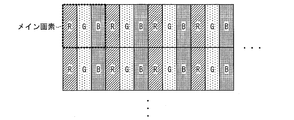
- FIG. 1 is a diagram illustrating an overall configuration of a liquid crystal display device according to an embodiment of the present invention.
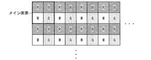
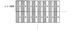
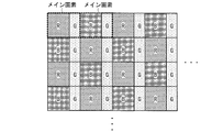
- FIG. 2 is a diagram showing an arrangement of sub-pixels constituting a main pixel provided in the display panel of the liquid crystal display device shown in FIG.
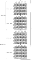
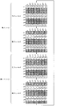
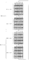
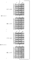
- FIG. 6 is a transition diagram schematically showing how the polarity of each sub-pixel changes when 1-dot inversion driving is performed while performing 1-line interlaced driving in the liquid crystal display device according to an embodiment of the present invention. is there. It is a timing chart which shows the relationship between a scanning signal and a data signal.
- FIG. 2 is a diagram showing an arrangement of sub-pixels constituting a main pixel provided in the display panel of the liquid crystal display device shown in FIG.
- FIG. 6 is a transition diagram schematically showing how the polarity of each sub-pixel changes when 1-dot inversion driving is performed while performing 1-line interlaced driving in the liquid crystal display device according to an embodiment of the present invention. is there. It is a timing chart which
- FIG. 6 is a transition diagram schematically showing how the polarity of each sub-pixel changes when 1-dot inversion driving is performed while performing 1-line interlaced driving in the liquid crystal display device according to an embodiment of the present invention. is there.
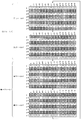
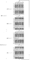
- FIG. 6 is a transition diagram schematically showing how the polarity of each sub-pixel changes when 2-dot inversion driving is performed while performing 1-line interlaced driving in the liquid crystal display device according to an embodiment of the present invention. is there.
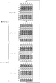
- FIG. 6 is a transition diagram schematically showing how the polarity of each sub-pixel changes when 2-dot inversion driving is performed while performing 2-line interlaced driving in the liquid crystal display device according to an embodiment of the present invention. is there.
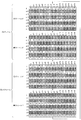
- FIG. 6 is a transition diagram schematically showing how the polarity of each sub-pixel changes when 2-dot inversion driving is performed while performing 2-line interlaced driving in the liquid crystal display device according to an embodiment of the present invention. is there.
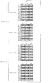
- FIG. 6 is a transition diagram schematically showing how the polarity of each sub-pixel changes when performing one-dot inversion driving while performing one-line interlaced driving in a liquid crystal display device according to another embodiment of the present invention. It is.
- FIG. 7 is a transition diagram schematically showing how the polarity of each sub-pixel changes when performing 2-dot inversion driving while performing 1-line interlaced driving in a liquid crystal display device according to another embodiment of the present invention. It is.
- FIG. 7 is a transition diagram schematically showing how the polarity of each sub-pixel changes when performing one-dot inversion driving while performing two-line interlaced driving in a liquid crystal display device according to another embodiment of the present invention. It is.
- FIG. 7 is a transition diagram schematically showing how the polarity of each sub-pixel changes when performing 2-dot inversion driving while performing 2-line interlaced driving in a liquid crystal display device according to another embodiment of the present invention. It is. FIG. 7 is a transition diagram schematically showing how the polarity of each sub-pixel changes when performing 2-dot inversion driving while performing 2-line interlaced driving in a liquid crystal display device according to another embodiment of the present invention. It is. It is a figure which is provided in the display panel of the liquid crystal display device which concerns on further another embodiment of this invention, and shows arrangement
- liquid crystal display device when the 1-line interlace drive and the 1-dot inversion drive are performed, how the polarity of each sub-pixel changes is schematically illustrated. It is a transition diagram. In the liquid crystal display device according to yet another embodiment of the present invention, how the polarity of each sub-pixel changes when performing 1-line interlaced driving and 2-dot inversion driving is schematically shown. It is a transition diagram. In a liquid crystal display device according to still another embodiment of the present invention, how the polarity of each sub-pixel changes when performing two-line interlaced driving and one-dot inversion driving is schematically shown. It is a transition diagram.
- liquid crystal display device In the liquid crystal display device according to still another embodiment of the present invention, how the polarity of each sub-pixel changes when performing 2-line interlace driving and 2-dot inversion driving is schematically shown. It is a transition diagram. In the liquid crystal display device according to still another embodiment of the present invention, how the polarity of each sub-pixel changes when performing 2-line interlace driving and 2-dot inversion driving is schematically shown. It is a transition diagram. It is a figure which is provided in the display panel of the liquid crystal display device which concerns on further another embodiment of this surface, and shows arrangement
- a liquid crystal display device In a liquid crystal display device according to still another embodiment of the present invention, how the polarity of each sub-pixel changes when performing three-line interlaced driving and one-dot inversion driving is schematically shown. It is a transition diagram. In the liquid crystal display device according to still another embodiment of the present invention, how the polarity of each sub-pixel changes when performing 3-line interlace driving and 3-dot inversion driving is schematically shown. It is a transition diagram. In the flat display device disclosed in Patent Literature 1, scanning is performed by thinning out scanning lines for each line, and a timing chart in a case where one image is formed by two frames is shown. FIG. 6 is a transition diagram schematically showing how the polarity of each sub-pixel changes when performing m-dot inversion driving while performing one-line interlaced driving in the liquid crystal display device according to an embodiment of the present invention. is there.
- the display device is a liquid crystal display device including a display panel which is a liquid crystal display (LCD)
- LCD liquid crystal display
- the present invention is not limited to this. is not.
- the display device according to the present invention may be, for example, a PDP display device including a plasma display (PD), or an EL display device including an EL (Electro Luminescence) display.
- FIG. 1 is a diagram illustrating an overall configuration of a liquid crystal display device 1 according to Embodiment 1.
- FIG. 1 is a diagram illustrating an overall configuration of a liquid crystal display device 1 according to Embodiment 1.
- a liquid crystal display device 1 includes a display panel (liquid crystal display panel) 2, a timing controller 4 (control means), a scanning line driving circuit 6 (gate line driving circuit), and a signal line driving circuit 8 (data line). Drive circuit), a common electrode drive circuit 10, and a power supply generation circuit 13.
- the display panel 2 has a total of P rows (where P is an integer equal to or greater than 1) scanning lines (gate lines), and a total number of Q columns (Q is an integer equal to or greater than 1) arranged so as to intersect the scan lines. ) Data signal lines (data lines) and a plurality of sub-pixels arranged corresponding to the intersections of the scanning lines and the data signal lines. As will be described later, a predetermined number of sub-pixels constitute a main pixel (picture element) as one group.
- the timing controller 4 uses the gate output control signal GOE to control the timing at which the scanning line driving circuit 6 scans (selects) the scanning line.
- the timing controller 4 controls the polarity of the data signal supplied from the signal line drive circuit 8 using the polarity inversion signal.
- the timing controller 4 supplies a scanning signal (gate signal) to a scanning line (selected scanning line) selected in a certain field, and then selects a scanning line selected next to the selected scanning line.
- the signal line drive current (data line drive current) I2 supplied to an arbitrary data line during the period until the scan signal is supplied is transferred to the arbitrary data line when the scan signal is supplied to the selected scan line.
- the signal line drive circuit 8 is controlled so as to be reduced by a predetermined rate compared to the supplied signal line drive current I1.
- the arbitrary data line may be a part of the data line of the Q column or all of the data lines of the Q column.
- the signal line drive circuit 8 drives the signal line drive current I2 to decrease by a predetermined rate compared to the signal line drive current I1 in accordance with an instruction from the timing controller 4.
- the signal line driving circuit 8 sets the data signal line in a high impedance state, or reduces the signal line driving current capability of an output stage amplifier (so-called voltage follower) included in the signal line driving circuit 8.
- the drive current I2 may be reduced by a predetermined rate compared to the signal line drive current I1.
- the signal line driving current I2 may be driven so as to be reduced by about 30% compared to the signal line driving current I2.
- the signal line drive current I2 is about 70% of the signal line drive current I1.
- the signal line driving current I2 is reduced by 100% in the signal line driving circuit 8, thereby setting the signal line driving current I2 to 0 and setting the absolute value of the potential of the applied data signal to 0V.
- the signal line driving circuit 8 stops supplying the signal line driving current, that is, stops applying the data signal.
- the scanning line driving circuit 6 starts scanning the scanning line with the gate start pulse signal received from the timing controller 4 as a signal.
- the scanning line driving circuit 6 sequentially selects the selection voltage from the first scanning line of the display panel 2 for each scanning line in accordance with the gate clock signal GCK and the gate output control signal GOE received from the timing controller 4. Is applied.
- the scanning line driving circuit 6 sequentially supplies a scanning signal, which is a voltage for turning on a switching element (TFT) provided in each sub-pixel on the scanning line, to each scanning line. Accordingly, the scanning line driving circuit 6 sequentially selects and scans each scanning line. Note that supplying a scanning signal that is a voltage for turning on the switching element is hereinafter referred to as scanning a scanning line.
- the scanning line driving circuit 6 sequentially selects each scanning line according to the received gate clock GCK signal.
- the scanning line driving circuit 6 supplies the scanning line driving current (gate line driving current) to the selected scanning line at the timing when the falling edge of the received gate output control signal GOE is detected, thereby selecting the selected voltage. (That is, a scanning signal) is applied. Thereby, the scanning line driving circuit 6 scans the selected scanning line. Further, the scanning line driving circuit 6 can perform interlace driving, as will be described later.
- applying a scanning signal to a scanning line by supplying a scanning line driving current is also simply referred to as applying (or supplying) the scanning signal.
- the signal line driving circuit 8 stores the input image data of each sub-pixel in a register according to the source clock signal based on the source start pulse signal received from the timing controller 4. Further, the signal line driving circuit 8 supplies a data signal, which is image data, to each data signal line of the display panel 2 in accordance with the next source latch strobe signal, and a pixel electrode provided in a sub-pixel including each data signal line. To charge.
- the signal line drive circuit 8 calculates the value of the voltage to be output to each sub-pixel on the selected scanning line based on the input video signal (arrow A), and the voltage ( That is, a data signal is output to each data signal line by supplying a signal line drive current. As a result, image data is supplied to each sub-pixel on the selected scanning line.
- applying a data signal to a data signal line by supplying a signal line driving current is simply expressed as applying (or supplying) the data signal.
- the signal line driving circuit 8 sets the polarity of the data signal applied to the selected pixel that is a sub-pixel to be selected in a certain field in accordance with the polarity inversion signal received from the timing controller 4 in the row direction and the column direction, respectively.
- the number of selected pixels is inverted as a unit, and the polarity of the data signal applied to each selected pixel in a certain field is set to the data applied to the selected pixel in the field immediately before the certain field. Invert with respect to signal polarity.
- the power generation circuit 13 generates a voltage necessary for each circuit in the liquid crystal display device 1 to operate. Then, the power supply generation circuit 13 outputs the generated voltage to the scanning line driving circuit 6, the signal line driving circuit 8, the timing controller 4, and the common electrode driving circuit 10.
- the liquid crystal display device 1 includes a common electrode (not shown) provided for each sub-pixel in the display panel 2.
- the common electrode drive circuit 10 outputs a predetermined common voltage for driving the common electrode to the common electrode based on a signal (arrow B) input from the timing controller 4 (arrow C).
- FIG. 2 is a diagram illustrating an arrangement of sub-pixels constituting the main pixel provided in the display panel 2 of the liquid crystal display device 1 according to the present embodiment.
- three sub-pixels that individually display the three primary colors (sub-pixel R that displays red, sub-pixel B that displays blue, and sub-pixel G that displays green), and three primary colors
- One main pixel (picture element) is configured with four sub-pixels of sub-pixels (sub-pixels W displaying white) that display one color obtained by combining at least one of them as a unit. Further, these four sub-pixels are arranged so as to be arranged two by two in the column direction and the row direction, respectively. For example, as shown in FIG.
- sub-pixel R and sub-pixel B, sub-pixel W and sub-pixel G is adjacent to each other in the row direction, and the sub pixel R and the sub pixel W, and the sub pixel B and the sub pixel G are adjacent to each other in the column direction.
- the sub-pixel R and the sub-pixel B, the sub-pixel W and the sub-pixel G are adjacent in the row direction, and the sub-pixel R and the sub-pixel W, the sub-pixel B and the sub-pixel G are in the column direction.
- the arrangement method of the four sub-pixels is 4 factorials, that is, 24 methods.
- the sub-pixel R and the sub-pixel G, the sub-pixel W and the sub-pixel B are adjacent to each other in the row direction.
- the pixel R, the sub-pixel W, the sub-pixel G, and the sub-pixel B may be arranged so as to be adjacent in the column direction.
- a case where four subpixels of a subpixel W that displays white are used as one color obtained by combining at least one of the three primary colors will be described as an example. It is not limited to this.
- the sub pixel W that displays white the sub pixel Y that displays yellow may be used, or only one of the three primary colors (either red, blue, or green) may be used.
- a configuration using sub-pixels for displaying other colors may be adopted.
- Interlaced drive When performing interlaced driving, one frame is divided into units called fields (a scanning line scanned in one frame is divided into a plurality of sets scanned in each field), and scanning is performed sequentially for each field. Go.
- the scanning line drive circuit 6 thins out the scanning lines for supplying scanning signals for each scanning line in a certain field (hereinafter also referred to as a first field). Scan by skipping one line.
- the scanning lines not scanned in the first field are scanned. That is, when the first field is configured by scanning odd-numbered scanning lines, the second field is configured by scanning even-numbered scanning lines.
- the present embodiment is not limited to the case where the first field and the second field are configured by scanning one scanning line, but scanning each field by scanning two scanning lines. You may comprise by.
- interlaced driving method in the i-th field, scanning is performed every j scanning lines in the order of kth, k + (j + 1) th, k + 2 (j + 1) th,.
- interlace driving is performed by scanning every j scanning lines in the order of k + 1, k + 1 + (j + 1) th, k + 1 + 2 (j + 1) th,... May be.
- the signal line driving circuit 8 selects the scanning line to be selected next to a certain scanning line from the time when the scanning line driving circuit 6 finishes selecting the scanning line in the first field of a certain frame. In the period until it is set, the data signal is driven to have a potential of 0V.
- the scanning line driving circuit 6 and the signal line driving circuit 8 operate in the second field of a certain frame in the same manner as the first field. Further, in the first field (or second field) of the next frame of a certain frame, the scanning line driving circuit 6 and the signal line driving circuit 8 operate in the same manner as the first field (or second field) of the certain frame. To do.
- the timing controller 4 when applying the scanning signal and the data signal using the interlace driving method, applies the scanning signal to the scanning line selected in a certain field, and then selects the selected one. Compare the signal line driving current in the period until the scanning signal is applied to the scanning line selected next to the scanning line to the signal line driving current when the scanning signal is applied to the selected scanning line. Then, the signal line driving circuit 8 is controlled so as to decrease by a predetermined rate.
- the signal is applied during the period from when the scanning signal is applied to the scanning line selected next to the selected scanning line.
- the power consumed to supply the line driving current can be reduced.
- the timing controller 4 applies the scanning signal to the scanning line selected after the selected scanning line after the scanning signal is applied to the scanning line selected in a certain field.
- the signal line driving circuit 8 is controlled so that the absolute value of the potential of the scanning signal is set to 0V by setting the supply of the signal line driving current to 0 in the period until the voltage is applied.
- the signal is applied during the period from when the scanning signal is applied to the scanning line selected next to the selected scanning line.
- the power consumed to supply the line drive current can be further reduced.
- the operation of the signal line driving circuit 8 described above may be used together with inversion driving or may not be used together.
- the operation of the signal line driving circuit 8 when operating in combination with inversion driving will be described below.
- FIG. 3 is a transition diagram schematically showing how the polarity of each sub-pixel changes in the liquid crystal display device 1 of the present embodiment.
- the first field includes p (where 1 ⁇ p ⁇ P-11) row scanning line, p + 2 row scanning line, p + 4 The scanning line in the row and the scanning line in the p + 6th row are scanned.
- the second field is configured by scanning the p + 1th scanning line, the p + 3th scanning line, the p + 5th scanning line, and the p + 7th scanning line. That is, the first field and the second field are configured by scanning one scan line at a time.
- the scanning line driving circuit 6 scans the pth scanning line, the p + 2th scanning line, the p + 4th scanning line, and the p + 6th row.
- the scanning lines are sequentially scanned.
- the scanning of the p + 1-th scanning line, the p + 3-th scanning line, the p + 5-th scanning line, and the p + 7-th scanning line, which are the scanning lines of the second field, is thinned out.
- the scanning line driving circuit 6 scans the scanning lines for each scanning line from the first scanning line to the Pth scanning line.
- the signal line driving circuit 8 performs q (where 1 ⁇ q ⁇ Q-15) A data signal having a polarity “+” is supplied to the data signal line in the column, and a data signal having a polarity “+” is supplied to the data signal line in the q + 1 column.
- the signal line driving circuit 8 supplies a data signal having a polarity of “ ⁇ ” to the data signal lines in the q + 2 column and the q + 3 column, and the data signals in the q + 4 column and the q + 5 column
- a data signal having a polarity “+” is supplied to the line
- a data signal having a polarity “ ⁇ ” is supplied to the data signal lines in the q + 6th column and the q + 7th column.
- the signal line driving circuit 8 thus operates when the scanning line driving circuit 6 scans the p-th scanning line to the Q-th data signal line. Until then, the data signal having the same polarity is supplied to each of the two sub-pixels arranged in the row direction constituting the main pixel indicated by the broken line in FIG. In other words, with respect to the row direction, the polarity of the data signal applied to each sub pixel is inverted with two sub pixels arranged in the row direction constituting the main pixel as one unit.
- the signal line driving circuit 8 has a polarity “ The data signal having “ ⁇ ” is supplied, and the data signal having the polarity “ ⁇ ” is supplied to the data signal line in the q + 1th column. Further, the signal line drive circuit 8 supplies a data signal having a polarity of “+” to the data signal lines in the q + 2 column and the q + 3 column, and the data signals in the q + 4 column and the q + 5 column. A data signal having a polarity of “ ⁇ ” is supplied to the line, and a data signal having a polarity of “+” is supplied to the data signal lines in the q + 6th column and the q + 7th column.
- the signal line driving circuit 8 shifts the main pixel from the first column data signal line to the Q column data signal line. Driving is performed so that data signals having the same polarity are supplied to every two sub-pixels arranged in the row direction.
- subpixels (hereinafter referred to as (p, q) -th) defined by the scanning line in the p-th row and the data signal line in the q-th column.
- the polarity of the data signal applied to R) (also referred to as a sub-pixel) is “+” as shown in FIG.
- the polarity of the data signal applied to the (p + 2, q) -th subpixel R and the (p, q + 2) -th subpixel R is “ ⁇ ” as shown in FIG.
- the polarity of the data signal applied to the (p, q + 1) th sub-pixel B is “+” as shown in FIG.
- the polarity of the data signal applied to the (p + 2, q + 1) th sub-pixel B and the (p, q + 3) -th sub-pixel B is “ ⁇ ” as shown in FIG.
- the signal line driving circuit 8 is a sub-pixel that displays the same color among the sub-pixels defined by the scanning lines scanned in the first field and is closest to each other.
- data signals having opposite polarities are applied.
- the signal line driving circuit 8 has two units of main pixels in the row direction and one sub-pixel in the column direction in one unit (that is, 2 ⁇ 1) in the row direction and the column direction, respectively.
- the polarity of the data signal applied to each selected pixel is inverted using the selected pixel group as one unit.
- the scanning line driving circuit 6 includes, in the second field of the x-th frame, the p + 1th scanning line, the p + 3th scanning line, the p + 5th scanning line, and the p + 7th.
- the scanning lines in the row are sequentially scanned.
- the scanning of the p-th scanning line, the p + 2th scanning line, the p + 4th scanning line, and the p + 6th scanning line as the first field is thinned out. In this way, scanning is performed with one scanning line skipped from the first scanning line to the Pth scanning line. Therefore, as shown in FIG. 3, the scanning line driving circuit 6 performs one-line interlaced driving by repeating scanning of the first field scanning line and scanning of the second field scanning line.
- the signal line driving circuit 8 applies the data signal line of the q-th column.
- a data signal having a polarity “+” is supplied, and a data signal having a polarity “+” is supplied to the data signal line in the q + 1th column.
- the signal line driving circuit 8 supplies a data signal having a polarity of “ ⁇ ” to the data signal lines in the q + 2 column and the q + 3 column, and the data signals in the q + 4 column and the q + 5 column
- a data signal having a polarity “+” is supplied to the line
- a data signal having a polarity “ ⁇ ” is supplied to the data signal lines in the q + 6th column and the q + 7th column.
- the signal line driving circuit 8 when the scanning line driving circuit 6 scans the p + 3th scanning line, the signal line driving circuit 8 has a polarity “ The data signal having “ ⁇ ” is supplied, and the data signal having the polarity “ ⁇ ” is supplied to the data signal line in the q + 1th column. Further, the signal line drive circuit 8 supplies a data signal having a polarity of “+” to the data signal lines in the q + 2 column and the q + 3 column, and the data signals in the q + 4 column and the q + 5 column. A data signal having a polarity of “ ⁇ ” is supplied to the line, and a data signal having a polarity of “+” is supplied to the data signal lines in the q + 6th column and the q + 7th column.
- the signal line driving circuit 8 thus operates when the scanning line driving circuit 6 scans the p-th scanning line to the Q-th data signal line. Up to this time, driving is performed so as to supply data signals having the same polarity for every two sub-pixels arranged in the row direction.
- the polarity of the data signal applied to the (p + 1, q) th sub-pixel W is “+” as shown in FIG. It becomes the polarity. Further, the polarity of the data signal applied to the (p + 3, q) th sub-pixel W and the (p + 1, q + 2) -th subpixel W is “ ⁇ ” as shown in FIG.
- the polarity of the data signal applied to the (p + 1, q + 1) th sub-pixel G is “+” as shown in FIG.
- the polarity of the data signal applied to the (p + 3, q + 1) th sub-pixel B and the (p + 1, q + 3) -th subpixel B is “ ⁇ ” as shown in FIG.
- the signal line driving circuit 8 is a sub-pixel displaying the same color among the sub-pixels defined by the scanning lines scanned in the second field, and the polarities of the sub-pixels closest to each other are mutually different. Apply the opposite data signal.
- the polarity of the data signal applied to each selected pixel selected in a certain field is the polarity of the data signal applied to the selected pixel in the field immediately before the certain field. Is reversed with respect to.
- the scanning line driving circuit 6 repeats scanning and non-scanning for each field with respect to each scanning line, and the signal line driving circuit 8 performs data signal supply to each data signal line for each frame. Drive to reverse polarity.
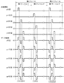
- FIG. 4 is a timing chart showing the relationship between the scanning signal and the data signal.
- a scanning signal having a high level (H level) voltage is applied to the p-th scanning line at time T1 (that is, the p-th scanning line).
- supply of data signals having a polarity of “+” is started to the data signal lines in the q-th, q + 1-th and q + 4-th columns, as shown in FIG. .
- supply of a data signal having a polarity of “ ⁇ ” is started to the data signal lines in the q + 2 and q + 3 columns.
- the potential of the data signal supplied to each data signal line becomes 0 V substantially simultaneously with the selection of the scanning line in the p-th row at time T2. That is, at time T2, the supply of the data signal to each data signal line is stopped. The stop of the supply of the data signal is maintained until the p + 2th scanning line is selected at time T3.
- the supply of a data signal having a polarity opposite to the polarity of is started.
- the potential of the data signal supplied to each data signal line becomes 0 V substantially at the same time when selection of the p-th scanning line is completed at time T12.
- a data signal having a polarity opposite to the polarity of the data signal supplied in the first field of the xth frame is applied to each data signal line.
- Supply is started.
- the potential of the data signal supplied to each data signal line becomes 0 V substantially at the same time when the scanning of the scanning line of the (p + 2) th row is completed at time T14.
- the timing controller 4 inverts the polarity of the data signal for each predetermined number of selected pixels and sets the polarity of the data signal applied to each selected pixel in a certain field to the field in which the selected pixel is selected.
- the signal line driving circuit 8 is controlled so as to invert the polarity of the data signal applied to the selected pixel in the field immediately before the certain field. As a result, the scanning line driving circuit 6 and the signal line driving circuit 8 are driven to apply the dot inversion driving to the gate line selected by the interlace driving.
- the timing controller 4 changes the polarity of the data signal applied to each selected pixel in the first field (or second field) of the xth frame to the first field (or the first field of the x + 1th frame).
- the signal line driver circuit is controlled so as to invert in (2 fields).
- the scanning line driving circuit 6 and the signal line driving circuit 8 perform 1-line interlaced driving and 1-dot inversion driving, they are arranged in the row direction constituting the main pixel in the row direction.
- the signal line driving circuit 8 is a sub-pixel that configures each main pixel adjacent to each other by applying data signals of different polarities to two sub-pixels arranged in the row direction constituting the main pixel in the row direction.
- a configuration may be adopted in which the polarity of the data signal applied to each subpixel is inverted with two subpixels adjacent in the row direction as one unit.
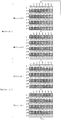
- FIG. 5 is a transition diagram schematically showing how the polarity of each sub-pixel changes in the liquid crystal display device 1 according to the present embodiment.
- the scanning line driving circuit 6 scans the p-th scanning line, the p + 2th scanning line, the p + 4th scanning line, and the p + 6th row.
- the scanning lines are sequentially scanned.
- the scanning of the p + 1-th scanning line, the p + 3-th scanning line, the p + 5-th scanning line, and the p + 7-th scanning line, which are the scanning lines of the second field, is thinned out.
- the scanning line driving circuit 6 scans scanning lines from the first scanning line to the P-th scanning line by skipping one line, and switches between scanning and non-scanning for each field. .
- the signal line driving circuit 8 is a sub-pixel constituting another main pixel, and applies a data signal having the same polarity to two sub-pixels adjacent in the row direction.
- the polarity of the data signal applied to each sub-pixel arranged adjacent to each other in the column direction among the sub-pixels defined by the scanning lines scanned in each field is inverted.
- the data signals applied to the (p, q + 1) th subpixel B and the (p, q + 2) th subpixel R are changed.
- the polarity is “+” as shown in FIG.
- the (p + 2, q + 1) th subpixel B, the (p, q + 3) th subpixel B, the (p + 2, q + 2) th subpixel R, and the (p, q + 4) th subpixel R are applied.
- the polarity of the data signal is “ ⁇ ” as shown in FIG.
- the polarity of the data signal applied to each selected pixel selected in a certain field is the polarity of the data signal applied to the selected pixel in the field immediately before the certain field. Is reversed with respect to.
- the scanning line driving circuit 6 repeats scanning and non-scanning for each field with respect to each scanning line, and the signal line driving circuit 8 performs data signal supply to each data signal line for each frame. Drive to reverse polarity.
- the supply of the data signal having the polarity shown in FIG. 5 is started to each data signal line almost simultaneously with the selection of the (p + 1) th scanning line (time t2).
- the potential of the supplied data signal becomes 0 V almost simultaneously with the selection of the scanning line of the (p + 1) th row, and is maintained until the scanning line of the (p + 3) th row is selected.
- the first field (or second field) of the (x + 1) th frame is applied to each data signal line substantially simultaneously with the selection of each scanning line.
- the supply of the data signal having the opposite polarity to the polarity of the data signal supplied in (1) is sequentially started.
- the potential of the data signal supplied to each data signal line becomes 0 V substantially simultaneously when the scanning of each scanning line is completed.
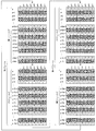
- FIG. 6 schematically shows how the polarity of each sub-pixel changes in the liquid crystal display device 1 according to the present embodiment when 1-line interlace driving is performed and 2-dot inversion driving is performed. It is a transition diagram.
- the scanning line driving circuit 6 scans the p-th scanning line, the p + 2th scanning line, the p + 4th scanning line, and the p + 6th row.
- the scanning lines are sequentially scanned.
- the scanning line driving circuit 6 scans the p + 1-th scanning line, the p + 3-th scanning line, the p + 5-th scanning line, and the p + 7-th scanning line that are the scanning lines of the second field. Is thinned out.
- the scanning line driving circuit 6 scans the scanning lines from the first scanning line to the P-th scanning line, skipping one line, and switching between scanning and non-scanning for each field. .
- the signal line driving circuit 8 applies a data signal having the same polarity to each of the two sub-pixels arranged in the row direction constituting the main pixel.
- the polarity of the data signal applied to each sub-pixel arranged adjacent to each other in the column direction among the sub-pixels defined by the scanning lines scanned in each field is inverted.
- the signal line driving circuit 8 performs the row direction that constitutes the main pixel from the first data signal line to the Qth data signal line. Are driven so as to supply data signals of the same polarity to the two sub-pixels arranged in a row.
- the data signals applied to the (p, q) th subpixel R and the (p + 2, q) th subpixel R The polarity is “+” as shown in FIG. Further, it is applied to the (p + 4, q) th subpixel R, the (p + 6, q) th subpixel R, the (p, q + 2) th subpixel R, and the (p + 2, q + 2) th subpixel R.
- the polarity of the data signal is “ ⁇ ” as shown in FIG.
- the polarities of the data signals applied to the (p + 1, q) th subpixel W and the (p + 3, q) th subpixel W in the second field of the xth frame are shown in FIG.
- the polarity is “+”.
- the (p + 5, q) th subpixel W, the (p + 7, q) th subpixel W, the (p + 1, q + 2) th subpixel W, and the (p + 3, q + 2) th subpixel W are applied.
- the polarity of the data signal is “ ⁇ ” as shown in FIG.
- the signal line driving circuit 8 is a sub-pixel that displays the same color among the sub-pixels defined by the scanning lines scanned in the first field or the second field of the x-th frame.
- the data signal is supplied so that the polarity is inverted every two sub-pixels closest to each other in the column direction and the polarity of each sub-pixel closest to the row direction is inverted, thereby performing 2-dot inversion driving.
- the signal line driving circuit 8 includes two sub-pixels constituting the main pixel in the row direction and two sub-pixels in the column direction in one unit (that is, in the row direction and the column direction).
- the polarity of the data signal applied to each selected pixel is inverted using a 2 ⁇ 2 selected pixel group as one unit.
- the polarity of the data signal applied to each selected pixel selected in a certain field is the polarity of the data signal applied to the selected pixel in the field immediately before the certain field. Is reversed with respect to.
- the supply of the data signal having the polarity shown in FIG. 6 is started to each data signal line substantially simultaneously with the selection of the p-th scanning line (time t3).
- the potential of the supplied data signal becomes 0 V substantially simultaneously with the end of scanning of the p-th scanning line, and is maintained until the p + 2th scanning line is selected.
- the supply of the data signal having the polarity shown in FIG. 6 is started to each data signal line substantially simultaneously with the selection of the (p + 1) th scanning line (time t4).
- the potential of the data signal supplied to each data signal line becomes 0 V substantially at the same time as the selection of the p + 1-th scanning line is completed, and is maintained until the p + 3-th scanning line is selected.
- the first field (or second field) of the (x + 1) th frame is applied to each data signal line substantially simultaneously with the selection of each scanning line.
- the supply of the data signal having the opposite polarity to the polarity of the data signal supplied in (1) is sequentially started.
- the potential of the data signal supplied to each data signal line becomes 0 V almost simultaneously with the selection of each scanning line.
- FIG. 7 schematically shows how the polarity of each sub-pixel changes in the liquid crystal display device 1 according to the present embodiment when 2-line interlace driving is performed and 2-dot inversion driving is performed. It is a transition diagram.
- the first field includes p-th scanning line, p + 3-th scanning line, p + 4-th scanning line, and p + 7-th scanning line as shown in FIG. It shall be constituted by scanning.
- the second field is configured by scanning the p + 1-th scanning line, the p + 2-th scanning line, the p + 5-th scanning line, and the p + 6-th scanning line.
- the first field and the second field are configured by scanning with two scanning lines skipped.
- the scanning line driving circuit 6 scans the p-th scanning line, the p + 3th scanning line, the p + 4th scanning line, and the p + 7th row.
- the scanning lines are sequentially scanned.
- the scanning of the p + 1-th scanning line, the p + 2-th scanning line, the p + 5-th scanning line, and the p + 6-th scanning line as the second field is thinned out.
- the scanning line driving circuit 6 scans the scanning lines by skipping two rows from the first scanning line to the Pth scanning line, and switches between scanning and non-scanning for each field. .
- the signal line driving circuit 8 applies a data signal having the same polarity to each of the two sub-pixels arranged in the row direction constituting the main pixel. Further, the polarity of the data signal applied to each of the two subpixels arranged closest to each other in the column direction among the subpixels defined by the scanning lines scanned in each field is inverted.
- the signal line driving circuit 8 performs the row direction that constitutes the main pixel from the first data signal line to the Qth data signal line. Are driven so as to apply data signals of the same polarity to the two sub-pixels arranged in a row.
- the scanning line driving circuit 6 and the signal line driving circuit 8 perform the above-described driving, so that the data signal applied to the (p, q) th subpixel R and the (p + 3, q) th subpixel W.
- the polarity is “+” as shown in FIG.
- it is applied to the (p + 4, q) th subpixel R, the (p, q + 2) th subpixel R, the (p + 7, q) th subpixel W, and the (p + 3, q + 2) th subpixel W.
- the polarity of the data signal is “ ⁇ ” as shown in FIG.
- the polarities of the data signals applied to the (p + 1, q) th subpixel W and the (p + 2, q) th subpixel R in the second field of the xth frame are shown in FIG.
- the polarity is “+”.
- it is applied to the (p + 5, q) th subpixel W, the (p + 6, q) th subpixel R, the (p + 1, q + 2) th subpixel W, and the (p + 2, q + 2) th subpixel R.
- the polarity of the data signal is “ ⁇ ” as shown in FIG.
- the signal line driving circuit 8 is a sub-pixel that displays the same color among the sub-pixels defined by the scanning lines scanned in the first field or the second field of the first frame.
- the one-dot inversion drive is performed so that the polarity of the data signal applied to the subpixels closest to each other in the row direction and the column direction is inverted.
- the signal line driving circuit 8 has two sub-pixels constituting the main pixel adjacent in the row direction and two sub-pixels adjacent in the column direction as one unit in the row direction and the column direction, respectively.
- the polarity of the data signal applied to each selected pixel is inverted as a unit of 2 ⁇ 2 selected pixel groups.
- the polarity of the data signal applied to each selected pixel selected in a certain field is the polarity of the data signal applied to the selected pixel in the field immediately before the certain field. Is reversed with respect to.
- the supply of the data signal having the polarity shown in FIG. 7 is started to each data signal line substantially simultaneously with the selection of the (p + 1) th scanning line (time t6).
- the potential of the data signal supplied to each data signal line becomes 0 V substantially at the same time as the selection of the p + 2 row scanning line after the p + 1 row scanning line is selected. Maintained until selected.
- the first field (or second field) of the (x + 1) th frame is applied to each data signal line substantially simultaneously with the selection of each scanning line.
- the supply of the data signal having the opposite polarity to the polarity of the data signal supplied in (1) is sequentially started. Then, the potential of the data signal supplied to each data signal line becomes 0 V substantially simultaneously when the selection of each scanning line is completed.
- the signal line driving circuit 8 sets two sub-pixels arranged in the row direction constituting the main pixel to 1 in the row direction.
- the signal line driving circuit 8 applies data signals having different polarities to two sub-pixels adjacent to each other in the row direction in the row direction, and the sub-pixels forming the main pixels adjacent to each other.
- a configuration may be adopted in which the polarity of the data signal applied to each sub pixel is inverted with two sub pixels adjacent in the row direction as one unit.
- FIG. 8 is a transition diagram schematically showing how the polarity of each sub-pixel changes in the liquid crystal display device 1 according to the present embodiment.
- the scanning line driving circuit 6 scans the pth scanning line, the p + 3th scanning line, the p + 4th scanning line, and the p + 7th row.
- the scanning lines are sequentially scanned.
- the scanning of the p + 1-th scanning line, the p + 2-th scanning line, the p + 5-th scanning line, and the p + 6-th scanning line as the second field is thinned out.
- the scanning line driving circuit 6 scans the scanning lines from the first scanning line to the P-th scanning line, skipping two lines, and switching between scanning and non-scanning for each field. .
- the signal line driving circuit 8 is a sub-pixel constituting another main pixel, and applies a data signal having the same polarity to two sub-pixels adjacent in the row direction.
- the polarity of the data signal applied to each subpixel arranged closest to the column direction among the subpixels defined by the scanning lines scanned in each field is inverted.
- the signal line driving circuit 8 configures other main pixels from the first column data signal line to the Qth column data signal line when the scanning line driving circuit 6 scans the scanning line.
- the sub-pixel is driven so as to supply data signals having the same polarity to two sub-pixels adjacent in the row direction.
- the scanning line driving circuit 6 and the signal line driving circuit 8 perform the above-described driving, so that the data signal applied to the (p, q) th subpixel R and the (p + 3, q) th subpixel W.
- the polarity is “ ⁇ ” as shown in FIG.
- it is applied to the (p + 4, q) th subpixel R, the (p, q + 2) th subpixel R, the (p + 7, q) th subpixel W, and the (p + 3, q + 2) th subpixel W.
- the polarity of the data signal is “+” as shown in FIG.
- the polarities of the data signals applied to the (p + 1, q) th subpixel W and the (p + 2, q) th subpixel R in the second field of the xth frame are shown in FIG.
- the polarity is “ ⁇ ”.
- it is applied to the (p + 5, q) th subpixel W, the (p + 6, q) th subpixel R, the (p + 1, q + 2) th subpixel W, and the (p + 2, q + 2) th subpixel R.
- the polarity of the data signal is “+” as shown in FIG.
- the signal line drive circuit 8 is a sub-pixel displaying the same color in the first field or the second field, and the data signals having opposite polarities to the sub-pixels closest to each other. Supply.
- the signal line driving circuit 8 is adjacent to each other in the row direction and the column direction.
- the polarity of the data signal applied to each selected pixel is inverted using two subpixels as one unit.
- the polarity of the data signal applied to each selected pixel selected in a certain field is the polarity of the data signal applied to the selected pixel in the field immediately before the certain field. Is reversed with respect to.
- the signal line driving circuit 8 when performing 2-line interlaced driving and 2-dot inversion driving, is adjacent to the adjacent two lines in which scanning is thinned out in the first field of each frame in the column direction.
- the signal line driving circuit 8 has two adjacent sub-pixels defined by the scanning lines sandwiched between the two scanning lines thinned out in the first field of each frame in the column direction as one unit.
- a configuration in which the polarity of the data signal applied to each sub-pixel is inverted may be employed.
- FIG. 9 shows a case where the liquid crystal display device 1 according to the present embodiment is sandwiched between two scanning lines that are thinned out in the first field of each frame when performing two-line interlaced driving and two-dot inversion driving.
- the scanning line driving circuit 6 performs p-line scanning line, p + 3 scanning line, p + 4th scanning line in the first field of the x-th frame in order to perform 2-line interlace driving.
- the scanning line and the scanning line of the p + 7th row are sequentially scanned.
- the scanning of the p + 2th scanning line, the p + 3th scanning line, the p + 5th scanning line, and the p + 6th scanning line, which are the scanning lines of the second field, is thinned out.
- the scanning line driving circuit 6 thus scans the scanning lines every two scanning lines from the first scanning line to the Pth scanning line. That is, the scanning line driving circuit 6 repeats scanning and non-scanning for each scanning line for every two scanning lines, and switches between scanning and non-scanning for each field.
- the signal line driving circuit 8 applies a data signal with reversed polarity to each of two sub-pixels arranged adjacent to each other in the row direction and constituting the main pixel, and is adjacent to the main line adjacent to the row direction.
- the polarity of the data signal applied for each pixel is inverted.
- the polarity of the data signal to be applied is inverted for every two adjacent sub-pixels defined by the scanning lines sandwiched between two scanning lines to be thinned out in the first field.
- the signal line drive circuit 8 applies a data signal with the polarity reversed every frame to the same subpixel.
- the signal line drive circuit 8 allows the sub-pixels constituting the main pixel from the data signal line in the first column to the data signal line in the Q column when the scan line drive circuit 6 scans the scan line.
- the driving is performed so that data signals having the same polarity are applied to two sub-pixels adjacent in the row direction.
- the polarity of the data signal applied to each subpixel is applied to each corresponding subpixel in the first field of the xth frame.
- the opposite of the polarity of the data signal is opposite to the polarity of the data signal applied to each corresponding subpixel in the second field of the xth frame.
- the polarity of the data signal applied to each selected pixel selected in a certain field is the polarity of the data signal applied to the selected pixel in the field immediately before the certain field. Is reversed with respect to.
- FIG. 30 schematically shows how the polarity of each sub-pixel changes in the liquid crystal display device 1 according to the present embodiment when 1-line interlace driving is performed and m-dot inversion driving is performed. It is a transition diagram.
- m dots indicate “m rows ⁇ 2 columns” selected pixels among the scanning pixels corresponding to the selected scanning line in each field, but this does not limit the present embodiment.
- the first field and the second field in each frame are configured by scanning the scanning lines by skipping one line as shown in FIG.
- the scanning line driving circuit 6 scans each scanning line in the p, p + 2,..., P + 2m ⁇ 2, p + 2m,. Are sequentially scanned. In this way, the scanning line driving circuit 6 scans the scanning lines from the first scanning line to the P-th scanning line, skipping one line, and switching between scanning and non-scanning for each field. .
- the signal line driving circuit 8 applies a data signal having the same polarity to each of the two sub-pixels arranged in the row direction constituting the main pixel. Further, the polarity of the data signal applied to each of the two subpixels arranged closest to each other in the column direction among the subpixels defined by the scanning lines scanned in each field is inverted.
- the polarity of the data signal applied to the (p + 2m + 1, q) th,..., (P + 4m ⁇ 1, q) th subpixel W is “+”.
- the polarity of the signal is “-”.
- the polarity of the data signal applied to each subpixel is the same as that of the data signal applied to each corresponding subpixel in the first field of the xth frame. The opposite of polarity. Further, the polarity of the data signal applied to each sub-pixel in the second field of the (x + 1) th frame is opposite to the polarity of the data signal applied to each corresponding sub-pixel in the second field of the x-th frame. .
- the polarity of the data signal applied to each selected pixel selected in a certain field is the polarity of the data signal applied to the selected pixel in the field immediately before the certain field. Is reversed with respect to.
- the signal line driving circuit 8 is a sub-pixel that displays the same color among the sub-pixels defined by the scanning lines scanned in each field, and is m sub-pixels closest to each other in the column direction.
- the data signal is supplied so that the polarity is inverted for each pixel and the polarity is inverted for each sub-pixel closest to the row direction.
- the signal line driving circuit 8 is a sub-pixel displaying the same color among the sub-pixels constituting each picture element, and the polarity is inverted for each of the m sub-pixels closest to each other in the column direction, A data signal is supplied so that the polarity is inverted for each sub-pixel closest to the row direction.
- a liquid crystal display device according to another embodiment of the present invention will be described with reference to FIGS.
- FIG. 10 is a diagram showing an arrangement of four sub-pixels included in the display panel 2 of the liquid crystal display device 1 according to the present embodiment and constituting the main pixel.
- one main pixel is composed of four sub-pixels: a sub-pixel R, a sub-pixel B, a sub-pixel G, and a sub-pixel W.
- the four subpixels are arranged in a line in the row direction.
- the subpixel R, the subpixel G, the subpixel B, and the subpixel W are arranged in this order. Are arranged adjacent to each other in the row direction.
- the sub pixel R, the sub pixel G, the sub pixel B, and the sub pixel W are arranged adjacent to each other in the row direction.
- the arrangement method of the four sub-pixels is 4 factorials, that is, 24 methods.
- the sub-pixel R, the sub-pixel B, the sub-pixel G, and the sub-pixel W are adjacent in the row direction in this order. May be arranged.
- one main pixel is composed of four sub-pixels of a sub-pixel R, a sub-pixel B, a sub-pixel G, and a sub-pixel W
- the present invention is not limited to this.
- a configuration using the sub-pixel Y may be adopted, and of course, a configuration using sub-pixels for other colors may be adopted.
- FIG. 11 is a transition diagram schematically showing how the polarity of each sub-pixel changes in the liquid crystal display device 1 according to the present embodiment.
- the first field includes p-th scanning line, p + 2th scanning line, p + 4th scanning line, and p + 6th scanning line. It shall be constituted by scanning.
- the second field is configured by scanning the p + 1th scanning line, the p + 3th scanning line, the p + 5th scanning line, and the p + 7th scanning line. That is, the first field and the second field are configured by scanning one scan line at a time.
- the scanning line driving circuit 6 scans the p-th scanning line, the p + 2th scanning line, the p + 4th scanning line, and the p + 6th row.
- the scanning lines are sequentially scanned.
- the scanning of the p + 1-th scanning line, the p + 3-th scanning line, the p + 5-th scanning line, and the p + 7-th scanning line, which are the scanning lines of the second field, is thinned out.
- the scanning line driving circuit 6 scans the scanning lines for each scanning line from the first scanning line to the Pth scanning line.
- the signal line driving circuit 8 reads the data in the q-th column and the q + 2-th row.
- a data signal having a polarity “+” is supplied to the signal line, and a data signal having a polarity “ ⁇ ” is supplied to the data signal lines in the q + 1th column and the q + 3th row.
- the signal line drive circuit 8 supplies a data signal having a polarity of “ ⁇ ” to the data signal lines in the q + 4th column and the q + 6th column, and the polarity to the data signal line in the q + 5th column and the q + 7th column.
- a data signal that is “+” is supplied. Further, the signal line driving circuit 8 supplies a data signal having a polarity “+” to the data signal lines in the q + 8th column, the q + 10th column, the q + 13th column, and the q + 15th column, and the q + 9th column, the q + 11th column. A data signal having a polarity of “ ⁇ ” is supplied to the data signal lines in the first, q + 12th and q + 14th columns.
- the signal line driving circuit 8 applies the data signal lines in the qth column and the q + 2th row.
- a data signal having a polarity of “ ⁇ ” is supplied, and a data signal having a polarity of “+” is supplied to the data signal lines in the q + 1th column and the q + 3th row.
- the signal line driving circuit 8 supplies a data signal having a polarity of “+” to the data signal lines of the q + 4th column and the q + 6th column, and the polarity to the data signal line of the q + 5th column and the q + 7th column. Supply a data signal that is "-".
- the signal line driving circuit 8 supplies a data signal having a polarity of “ ⁇ ” to the data signal lines in the q + 8th column, the q + 10th column, the q + 13th column, and the q + 15th column, and the q + 9th column, the q + 11th column.
- a data signal having a polarity of “+” is supplied to the data signal lines of the first, q + 12th and q + 14th columns.
- the signal line driving circuit 8 is thus arranged so that when the scanning line driving circuit 6 scans the (p + 2) th scanning line, four signal lines are arranged adjacent to each other in the row direction constituting the main pixel. A data signal having an inverted polarity is applied to each sub pixel. Further, the signal line driving circuit 8 inverts the polarity of the data signal to be applied for each main pixel adjacent in the row direction.
- the polarities of the data signals applied to the (p, q) th subpixel R and the (p, q + 2) th subpixel B are as follows. As shown in FIG. 11, the polarity is “+”. Data applied to the (p + 2, q) th subpixel R, the (p, q + 4) th subpixel R, the (p + 2, q + 2) th subpixel B, and the (p, q + 6) th subpixel B. The polarity of the signal is “ ⁇ ” as shown in FIG.
- the polarity of the data signal applied to the (p, q + 1) th sub-pixel G and the (p, q + 3) -th sub-pixel W is “ ⁇ ” as shown in FIG.
- the polarity of the signal is “+” as shown in FIG.
- the polarities of the data signals applied to the (p + 1, q) th subpixel R and the (p + 1, q + 2) th subpixel B are as shown in FIG. “+” Polarity.
- the polarity of the signal is “ ⁇ ” as shown in FIG.
- the polarity of the data signal applied to the (p + 1, q + 1) th sub-pixel G and the (p + 1, q + 3) -th subpixel W is “ ⁇ ” as shown in FIG.
- the polarity of the signal is “+” as shown in FIG.
- the signal line driving circuit 8 is a sub-pixel displaying the same color among the sub-pixels defined by the scanning lines scanned in the first field, and data applied to the sub-pixels closest to each other. Drive so that the polarity of the signal is reversed.
- the polarity of the data signal applied to each subpixel is equal to the polarity of the data signal applied to each corresponding subpixel in the first field of the xth frame. The opposite of polarity. Further, the polarity of the data signal applied to each sub-pixel in the second field of the (x + 1) th frame is opposite to the polarity of the data signal applied to each corresponding sub-pixel in the second field of the x-th frame. .
- the polarity of the data signal applied to each selected pixel selected in a certain field is the polarity of the data signal applied to the selected pixel in the field immediately before the certain field. Is reversed with respect to.
- the scanning line driving circuit 6 performs one-line interlace driving for each scanning line, which repeats scanning and non-scanning for each scanning line and switches between scanning and non-scanning for each field.
- the signal line driving circuit 8 applies a data signal whose polarity is inverted for each sub-pixel to the four sub-pixels arranged adjacent to each other in the row direction and constituting the main pixel, and further in the row direction.
- One-dot inversion driving is performed to invert the polarity of the data signal applied to each adjacent main pixel.
- the signal line driving circuit 8 includes four sub-pixels constituting the main pixel in the row direction and one sub-pixel in the column direction in one unit (that is, in the row direction and the column direction).
- the polarity of the data signal applied to each selected pixel is inverted using a 4 ⁇ 1 selected pixel group as one unit.
- the signal line driving circuit 8 inverts the polarity of the data signal for each sub-pixel constituting the main pixel and also inverts the polarity of the data signal applied to each corresponding sub-pixel in the adjacent main pixels.
- a configuration can be adopted in which data signals having the same polarity are not applied to sub-pixels displaying the same color in the row direction.
- the supply of the data signal having the polarity shown in FIG. 11 is started to each data signal line substantially simultaneously with the selection of the p-th scanning line (time t7).
- the potential of the data signal supplied to each data signal line becomes 0V substantially at the same time as the selection of the p-th scanning line is completed, and is maintained until the p + 2th scanning line is selected.
- the supply of the data signal having the polarity shown in FIG. 11 is started to each data signal line substantially simultaneously with the selection of the (p + 1) th scanning line (time t8).
- the potential of the data signal supplied to each data signal line becomes 0 V substantially at the same time as the selection of the p + 1-th scanning line is completed, and is maintained until the p + 3-th scanning line is selected.
- the first field (or second field) of the (x + 1) th frame is applied to each data signal line substantially simultaneously with the selection of each scanning line.
- the supply of the data signal having the opposite polarity to the polarity of the data signal supplied in (1) is sequentially started.
- the potential of the data signal supplied to each data signal line becomes 0 V almost simultaneously with the selection of each scanning line.
- FIG. 12 schematically shows how the polarity of each sub-pixel changes in the liquid crystal display device 1 according to the present embodiment when 1-line interlace driving is performed and 2-dot inversion driving is performed. It is a transition diagram.
- the scanning line driving circuit 6 scans the pth scanning line, the p + 2th scanning line, the p + 4th scanning line, and the p + 6th scanning line.
- the scanning lines are sequentially scanned.
- the scanning line driving circuit 6 scans the p + 1-th scanning line, the p + 3-th scanning line, the p + 5-th scanning line, and the p + 7-th scanning line that are the scanning lines of the second field. Is thinned out.
- the scanning line driving circuit 6 scans the scanning lines from the first scanning line to the P-th scanning line, skipping one line, and switching between scanning and non-scanning for each field. .
- the signal line driving circuit 8 has four sub-pixels arranged adjacent to each other in the row direction constituting the main pixel during the scanning line driving circuit 6 scanning the scanning lines. On the other hand, a data signal with reversed polarity is applied to each sub-pixel. Further, the signal line driving circuit 8 inverts the polarity of the data signal to be applied for each main pixel adjacent in the row direction.
- the polarities of the data signals applied to the (p + 1, q + 1) th and (p + 3, q + 1) th subpixels G and the (p + 1, q + 3) th and (p + 3, q + 3) th subpixels W are as follows. As shown in FIG. 12, the polarity is “ ⁇ ”.
- the signal line driving circuit 8 has four sub-pixels constituting the main pixel in the row direction and two sub-pixels in the column direction in one unit (that is, in the row direction and the column direction).
- the polarity of the data signal applied to each selected pixel is inverted using a 4 ⁇ 2 selected pixel group as one unit.
- the polarity of the data signal applied to each selected pixel selected in a certain field is the polarity of the data signal applied to the selected pixel in the field immediately before the certain field. Is reversed with respect to.
- the scanning line driving circuit 6 repeats scanning and non-scanning for each scanning line for each scanning line, and switches between scanning and non-scanning for each field.
- the signal line driving circuit 8 applies a data signal whose polarity is inverted for each sub-pixel to four sub-pixels arranged adjacent to each other in the row direction and constituting the main pixel, and is adjacent in the row direction. The polarity of the data signal applied to each main pixel is inverted.
- the signal line driving circuit 8 further inverts the polarity of the data signal to be applied for every two subpixels adjacent in the column direction.
- the signal line drive circuit 8 inverts the polarity of the data signal for each sub-pixel constituting the main pixel, and further inverts the polarity of the data signal for each main pixel to display the same color in the row direction. It is possible to prevent a data signal having the same polarity from being applied to the pixel.
- the supply of the data signal having the polarity shown in FIG. 12 is started to each data signal line substantially simultaneously with the selection of the p-th scanning line (time t9).
- the potential of the data signal supplied to each data signal line becomes 0 V substantially simultaneously with the end of the selection of the p-th scanning line, and is maintained until the p + 2th scanning line is selected.
- the supply of the data signal having the polarity shown in FIG. 12 is started to each data signal line substantially simultaneously with the selection of the (p + 1) th scanning line (time t10).
- the potential of the data signal supplied to each data signal line becomes 0 V substantially at the same time as the selection of the p + 1-th scanning line is completed, and is maintained until the p + 3-th scanning line is selected.
- the first field (or second field) of the (x + 1) th frame is applied to each data signal line substantially simultaneously with the selection of each scanning line.
- the supply of the data signal having the opposite polarity to the polarity of the data signal supplied in (1) is sequentially started.
- the potential of the data signal supplied to each data signal line becomes 0 V almost simultaneously with the selection of each scanning line.
- FIG. 13 schematically shows how the polarity of each sub-pixel changes in the liquid crystal display device 1 according to the present embodiment when 2-line interlace driving is performed and 1-dot inversion driving is performed. It is a transition diagram.
- the scanning line driving circuit 6 has a p-th scanning line, a p + 3-th scanning line, and a p + 4-th row in the first field of the x-th frame.
- the scanning line and the scanning line of the p + 7th row are sequentially scanned.
- the scanning of the p + 2th scanning line, the p + 3th scanning line, the p + 5th scanning line, and the p + 6th scanning line which are the scanning lines of the second field, is thinned out.
- the scanning line driving circuit 6 scans the scanning lines from the first scanning line to the P-th scanning line, skipping two lines, and switching between scanning and non-scanning for each field. .
- the signal line driving circuit 8 includes four sub-pixels arranged adjacent to each other in the row direction constituting the main pixel when the scanning line driving circuit 6 scans the scanning line. On the other hand, a data signal with reversed polarity is applied to each sub-pixel. Further, the signal line driving circuit 8 inverts the polarity of the data signal to be applied for each main pixel adjacent in the row direction.
- the polarity of the data signal applied to is a “+” polarity as shown in FIG.
- the polarity of the signal is “ ⁇ ” as shown in FIG.
- the polarity of the data signal applied to the (p, q + 1) th sub-pixel G and the (p, q + 3) -th sub-pixel W is “ ⁇ ” as shown in FIG.
- the polarity of the signal is “+” as shown in FIG.
- the polarities of the data signals applied to the (p + 1, q) th subpixel R and the (p + 1, q + 2) th subpixel B are as shown in FIG. “+” Polarity.
- the polarity of the signal is “ ⁇ ” as shown in FIG.
- the polarity of the data signal applied to the (p + 1, q + 1) th sub-pixel G and the (p + 1, q + 3) -th subpixel W is a “ ⁇ ” polarity as shown in FIG.
- the polarity of the signal is “+” as shown in FIG.
- the signal line driving circuit 8 includes four sub-pixels constituting the main pixel in the row direction and one sub-pixel in the column direction in one unit (that is, in the row direction and the column direction).
- the polarity of the data signal applied to each selected pixel is inverted using a 4 ⁇ 1 selected pixel group as one unit.
- the polarity of the data signal applied to each selected pixel selected in a certain field is the polarity of the data signal applied to the selected pixel in the field immediately before the certain field. Is reversed with respect to.
- the scanning line driving circuit 6 repeats scanning and non-scanning of the scanning lines by skipping two lines for each scanning line, and further switches between scanning and non-scanning of the scanning lines for each field.
- the signal line driving circuit 8 applies a data signal with the polarity reversed for each sub-pixel to four sub-pixels arranged adjacent to each other in the row direction and constituting the main pixel.
- the polarity of the data signal applied every time is inverted.
- the signal line driver circuit 8 inverts the polarity of the data signal to be applied for each subpixel adjacent in the column direction. Further, the signal line drive circuit 8 applies a data signal with the polarity reversed every frame to the same subpixel.
- the supply of the data signal having the polarity shown in FIG. 13 is started to each data signal line almost simultaneously with the selection of the p-th scanning line (time t11).
- the potential of the data signal supplied to each data signal line becomes 0 V substantially at the same time as the selection of the p-th scanning line is completed, and is maintained until the p + 3th scanning line is selected.
- the supply of the data signal having the polarity shown in FIG. 13 is started to each data signal line substantially simultaneously with the selection of the (p + 1) th scanning line (time t12). .
- the potential of the data signal supplied to each data signal line becomes 0 V substantially at the same time as the selection of the p + 2 row scanning line after the p + 1 row scanning line is selected. Maintained until selected.
- the first field (or second field) of the (x + 1) th frame is applied to each data signal line substantially simultaneously with the selection of each scanning line.
- the supply of the data signal having the opposite polarity to the polarity of the data signal supplied in (1) is sequentially started.
- the potential of the data signal supplied to each data signal line becomes 0 V almost simultaneously with the selection of each scanning line.
- FIG. 14 schematically shows how the polarity of each sub-pixel changes in the liquid crystal display device 1 according to the present embodiment when 2-line interlace driving is performed and 1-dot inversion driving is performed. It is a transition diagram.
- the scanning line driving circuit 6 performs the p-th scanning line, the p + 3th scanning line, and the p + 4th row in the first field of the x-th frame.
- the scanning line and the scanning line of the p + 7th row are sequentially scanned.
- the scanning of the p + 2th scanning line, the p + 3th scanning line, the p + 5th scanning line, and the p + 6th scanning line which are the scanning lines of the second field, is thinned out.
- the scanning line driving circuit 6 scans the scanning lines every two scanning lines from the first scanning line to the Pth scanning line.
- the signal line driving circuit 8 includes four sub-pixels arranged adjacent to each other in the row direction constituting the main pixel when the scanning line driving circuit 6 scans the scanning line.
- a data signal with the polarity reversed is applied to each sub-pixel, and the polarity of the data signal applied to each main pixel adjacent in the row direction is reversed.
- the signal line driving circuit 8 has four sub-pixels constituting the main pixel in the row direction and two sub-pixels in the column direction in one unit (that is, in the row direction and the column direction).
- the polarity of the data signal applied to each selected pixel is inverted using a 4 ⁇ 2 selected pixel group as one unit.
- the signal line driving circuit 8 applies a data signal with the polarity reversed for each sub-pixel to four sub-pixels arranged adjacent to each other in the row direction and constituting the main pixel.
- the polarity of the data signal applied every time is inverted.
- the signal line driver circuit 8 inverts the polarity of the data signal to be applied for every two sub-pixels adjacent in the column direction.
- the signal line drive circuit 8 applies a data signal with the polarity reversed every frame to the same subpixel.
- the supply of the data signal having the polarity shown in FIG. 14 is started to each data signal line substantially simultaneously with the selection of the p-th scanning line (time t13).
- the potential of the data signal supplied to each data signal line becomes 0 V substantially simultaneously with the completion of the selection of the p-th scanning line, and is maintained until the p + 3th scanning line is selected.
- the supply of the data signal having the polarity shown in FIG. 14 is started to each data signal line substantially simultaneously with the selection of the (p + 1) th scanning line (time t14).
- the potential of the data signal supplied to each data signal line becomes 0 V substantially at the same time when the selection of the p + 2 row scanning line is completed after the p + 1 row scanning line is selected.
- the first field (or second field) of the (x + 1) th frame is applied to each data signal line substantially simultaneously with the selection of each scanning line.
- the supply of the data signal having the opposite polarity to the polarity of the data signal supplied in (1) is sequentially started.
- the potential of the data signal supplied to each data signal line becomes 0 V almost simultaneously with the selection of each scanning line.
- the signal line driving circuit 8 when performing 2-line interlaced driving and 2-dot inversion driving, is adjacent to the adjacent two lines in which scanning is thinned out in the first field of each frame in the column direction.
- a data signal to be applied to each sub-pixel with two sub-pixels defined by scanning lines sandwiching the scanning lines of the rows (for example, the p-th and p + 3th scanning lines in FIG. 14) as one unit.
- the signal line driving circuit 8 has two adjacent sub-pixels defined by the scanning lines sandwiched between the two scanning lines thinned out in the first field of each frame in the column direction as one unit.
- a configuration in which the polarity of the data signal applied to each sub-pixel is inverted may be employed.
- FIG. 15 shows a case where the liquid crystal display device 1 according to this embodiment is sandwiched between two scanning lines that are thinned out in the first field of each frame when performing two-line interlaced driving and two-dot inversion driving.
- the scanning line driving circuit 6 performs the two-line interlaced driving in the first field of the x-th frame, the p-th scanning line, the p + 3-th scanning line, and the p + 4-th line.
- the scanning line and the scanning line of the p + 7th row are sequentially scanned.
- the scanning of the p + 2th scanning line, the p + 3th scanning line, the p + 5th scanning line, and the p + 6th scanning line which are the scanning lines of the second field, is thinned out.
- the scanning line driving circuit 6 thus scans the scanning lines every two scanning lines from the first scanning line to the Pth scanning line. That is, the scanning line driving circuit 6 repeats scanning and non-scanning for each scanning line for every two scanning lines, and switches between scanning and non-scanning for each field.
- the signal line driving circuit 8 applies a data signal with the polarity reversed for each sub-pixel to four sub-pixels arranged adjacent to each other in the row direction and constituting the main pixel.
- the polarity of the data signal applied every time is inverted.
- the signal line driving circuit 8 inverts the polarity of the data signal to be applied for every two subpixels defined by the scanning lines adjacent to each other in the column direction between the scanning lines to be thinned. Further, the signal line drive circuit 8 applies a data signal with the polarity reversed every frame to the same subpixel.
- the polarity of the data signal applied to each subpixel is applied to each corresponding subpixel in the first field of the xth frame.
- the opposite of the polarity of the data signal is opposite to the polarity of the data signal applied to each corresponding subpixel in the second field of the xth frame.
- the polarity of the data signal applied to each selected pixel selected in a certain field is the polarity of the data signal applied to the selected pixel in the field immediately before the certain field. Is reversed with respect to.
- the case where the four sub-pixels constituting the main pixel are arranged so as to be arranged two each in the column direction and the row direction has been described as an example, but the present invention is not limited thereto. It is not something.
- the number of sub-pixels constituting the main pixel may be three, and a configuration in which the three sub-pixels constituting the main pixel are arranged in a line in the row direction may be employed.
- a liquid crystal display device according to still another embodiment of the present invention will be described with reference to FIGS.
- FIG. 16 is a diagram showing an arrangement of three sub-pixels included in the display panel 2 of the liquid crystal display device 1 according to the present embodiment and constituting the main pixel.
- one main pixel is composed of three sub-pixels: a sub-pixel R, a sub-pixel G, and a sub-pixel B.
- the three sub-pixels are arranged in a row in the row direction.
- the sub-pixel R, the sub-pixel G, and the sub-pixel B are arranged in the row direction in this order. Adjacent to each other.
- the case where the sub pixel R, the sub pixel G, and the sub pixel B are arranged adjacent to each other in the row direction will be described as an example. It is not limited.
- the three sub-pixels are arranged in the factorial of 3, that is, in six ways.
- the sub-pixel R, the sub-pixel B, and the sub-pixel G are arranged adjacent to each other in the row direction. It may be.
- FIG. 17 schematically shows how the polarity of each sub-pixel changes when performing 1-dot inversion driving while performing 1-line interlaced driving in the liquid crystal display device 1 according to the present embodiment. It is a transition diagram.
- the first field includes p-th scanning line, p + 2th scanning line, p + 4th scanning line, and p + 6th scanning line as shown in FIG. It shall be constituted by scanning.
- the second field is configured by scanning the p + 1th scanning line, the p + 3th scanning line, the p + 5th scanning line, and the p + 7th scanning line. That is, the first field and the second field are configured by scanning one scan line at a time.
- the scanning line driving circuit 6 scans the p-th scanning line, the p + 2th scanning line, the p + 4th scanning line, and the p + 6th row.
- the scanning lines are sequentially scanned.
- the scanning of the p + 1-th scanning line, the p + 3-th scanning line, the p + 5-th scanning line, and the p + 7-th scanning line, which are the scanning lines of the second field, is thinned out.
- the scanning line driving circuit 6 scans the scanning lines for each scanning line from the first scanning line to the Pth scanning line.
- the signal line driving circuit 8 when the scanning line driving circuit 6 scans the p-th scanning line in the first field of the x-th frame, the signal line driving circuit 8 reads the q-th column, the q + 2-th row, and Q + 4, a data signal having a polarity of “+” is supplied to the data signal line in the fourth row.
- the signal line driving circuit 8 supplies a data signal having a polarity of “ ⁇ ” to the data signal lines in the q + 1th column, the q + 3th row, and the q + 5th column.
- the signal line driving circuit 8 In the first field of the x-th frame, when the scanning line driving circuit 6 scans the p + 2th scanning line, the signal line driving circuit 8 reads the qth column, the q + 2th row, and the q + 4th row. A data signal having a polarity of “ ⁇ ” is supplied to the data signal line. The signal line driving circuit 8 supplies a data signal having a polarity of “+” to the data signal lines in the q + 1th column, the q + 3th row, and the q + 5th column.
- the signal line driving circuit 8 performs 1 on the sub-pixels arranged adjacent to each other in the row direction when the scanning line driving circuit 6 scans the p-th scanning line. A data signal having an inverted polarity is applied to each sub-pixel. The signal line driving circuit 8 also outputs a data signal that is inverted in polarity from the data signal applied when the scanning line driving circuit 6 scans the scanning line of the p + 2th column. Apply.
- the polarity of the data signal applied to is a “+” polarity.
- the polarity of the signal is “ ⁇ ” as shown in FIG.
- the polarity of the data signal applied to the (p, q + 1) -th subpixel G is “ ⁇ ” polarity
- the polarity of the data signal applied to the sub-pixel G is “+”.
- the signal line driving circuit 8 is driven so that the polarity of the data signal applied to the adjacent sub-pixel defined by the scanning line scanned in the first field is inverted. Further, the signal line drive circuit 8 inverts the polarity of the data signal applied to the adjacent sub-pixels among the sub-pixels that display the same color and are defined by the scanning lines scanned in the first field. To drive.
- the polarity of the data signal applied to the (p + 1, q) th subpixel R and the (p + 1, q + 2) th subpixel B is as shown in FIG. “+” Polarity.
- the polarity of the signal is “ ⁇ ” as shown in FIG.
- the polarity of the data signal applied to the (p + 1, q + 1) th sub-pixel G is “ ⁇ ”, and the (p + 3, q + 1) -th subpixel G, (p , Q + 4) The polarity of the data signal applied to the sub-pixel G is “+”.
- the signal line driving circuit 8 uses each subpixel as one unit (that is, 1 ⁇ 1 selected pixel group as one unit) in each field in the row direction and the column direction.
- the polarity of the data signal applied to is inverted.
- the polarity of the data signal applied to each selected pixel selected in a certain field is the polarity of the data signal applied to the selected pixel in the field immediately before the certain field. Is reversed with respect to.
- the supply of the data signal having the polarity shown in FIG. 17 is started to each data signal line substantially simultaneously with the selection of the (p + 1) th scanning line (time t16).
- the potentials of these data signals become 0 V substantially at the same time when selection of the scanning line of the (p + 1) th row is completed, and is maintained until the scanning line of the (p + 3) th row is selected.
- the first field (or second field) of the (x + 1) th frame is applied to each data signal line substantially simultaneously with the selection of each scanning line.
- the supply of the data signal having the opposite polarity to the polarity of the data signal supplied in (1) is sequentially started.
- the potential of the data signal supplied to each data signal line becomes 0 V almost simultaneously with the selection of each scanning line.
- FIG. 18 schematically shows how the polarity of each sub-pixel changes in the liquid crystal display device 1 according to the present embodiment when 1-line interlace driving is performed and 2-dot inversion driving is performed. It is a transition diagram.
- the scanning line driving circuit 6 scans the pth scanning line, the p + 2th scanning line, the p + 4th scanning line, and the p + 6th scanning line.
- the scanning lines are sequentially scanned.
- the scanning of the p + 1-th scanning line, the p + 3-th scanning line, the p + 5-th scanning line, and the p + 7-th scanning line, which are the scanning lines of the second field, is thinned out.
- the scanning line driving circuit 6 scans the scanning lines for each scanning line from the first scanning line to the Pth scanning line. That is, the scanning line driving circuit 6 repeats scanning and non-scanning for each scanning line for each scanning line, and switches between scanning and non-scanning for each field.
- the signal line driving circuit 8 inverts the polarity of the data signal applied to each subpixel with respect to the subpixels arranged adjacent to each other in the row direction in each field.
- the polarity of the data signal applied to every two subpixels adjacent in the column direction is inverted.
- the signal line driving circuit 8 inverts the polarity of the data signal applied to each subpixel for each frame.
- the signal line driving circuit 8 selects one sub-pixel in the row direction and two sub-pixels in the column direction in one unit (that is, 1 ⁇ 2 selection) in each field.
- the polarity of the data signal applied to each selected pixel is inverted using a pixel group as one unit.
- the polarity of the data signal applied to each subpixel is applied to each corresponding subpixel in the first field of the xth frame.
- the opposite of the polarity of the data signal is opposite to the polarity of the data signal applied to each corresponding subpixel in the second field of the xth frame.
- the polarity of the data signal applied to each selected pixel selected in a certain field is the polarity of the data signal applied to the selected pixel in the field immediately before the certain field. Is reversed with respect to.
- the supply of the data signal having the polarity shown in FIG. 18 is started to each data signal line substantially simultaneously with the selection of the p-th scanning line (time t17).
- the potential of the data signal supplied to each data signal line becomes 0V substantially at the same time as the selection of the p-th scanning line is completed, and is maintained until the p + 2th scanning line is selected.
- the supply of the data signal having the polarity shown in FIG. 18 is started to each data signal line substantially simultaneously with the selection of the (p + 1) th scanning line (time t18).
- the potential of the data signal supplied to each data signal line becomes 0 V substantially at the same time as the selection of the p + 1-th scanning line is completed, and is maintained until the p + 3-th scanning line is selected.
- the first field (or second field) of the (x + 1) th frame is applied to each data signal line substantially simultaneously with the selection of each scanning line.
- the supply of the data signal having the opposite polarity to the polarity of the data signal supplied in (1) is sequentially started.
- the potential of the data signal supplied to each data signal line becomes 0 V substantially simultaneously with the selection of each scanning line.
- FIG. 19 schematically shows how the polarity of each sub-pixel changes in the liquid crystal display device 1 according to the present embodiment when 2-line interlace driving is performed and 1-dot inversion driving is performed. It is a transition diagram.
- the scanning line driving circuit 6 scans the p-th scanning line, the p + 3th scanning line, the p + 4th scanning line, and the p + 7th row.
- the scanning lines are sequentially scanned.
- the scanning of the p + 1-th scanning line, the p + 2-th scanning line, the p + 5-th scanning line, and the p + 6-th scanning line which are the scanning lines of the second field, is thinned out.
- the scanning line driving circuit 6 scans the scanning lines every two scanning lines from the first scanning line to the Pth scanning line. That is, the scanning line driving circuit 6 repeats scanning and non-scanning every two scanning lines for each scanning line, and switches between scanning and non-scanning of the scanning lines every field.
- the signal line driving circuit 8 applies a data signal with the polarity reversed for each sub-pixel to the three sub-pixels arranged adjacent to each other in the row direction and constituting the main pixel, and is adjacent in the row direction.
- the polarity of the data signal applied to each main pixel to be reversed is inverted.
- the polarity of the data signal applied to each sub-pixel arranged adjacent to each other in the column direction among the sub-pixels defined by the scanning lines scanned in each field is inverted.
- the signal line drive circuit 8 sets the polarity of the data signal to be applied to each sub pixel with respect to the sub pixels arranged adjacent to each other in the row direction and the column direction. Invert. Further, the signal line driving circuit 8 inverts the polarity of the data signal applied to each subpixel for each frame.
- the signal line driving circuit 8 uses each subpixel as one unit (that is, 1 ⁇ 1 selected pixel group as one unit) in each field in the row direction and the column direction.
- the polarity of the data signal applied to is inverted.
- the polarity of the data signal applied to each subpixel is applied to each corresponding subpixel in the first field of the xth frame.
- the opposite of the polarity of the data signal is opposite to the polarity of the data signal applied to each corresponding subpixel in the second field of the xth frame.
- the polarity of the data signal applied to each selected pixel selected in a certain field is the polarity of the data signal applied to the selected pixel in the field immediately before the certain field. Is reversed with respect to.
- the first field (or second field) of the (x + 1) th frame is applied to each data signal line substantially simultaneously with the selection of each scanning line.
- the supply of the data signal having the opposite polarity to the polarity of the data signal supplied in (1) is sequentially started.
- the potential of the data signal supplied to each data signal line becomes 0 V substantially simultaneously with the selection of each scanning line.
- FIG. 20 schematically shows how the polarity of each sub-pixel changes in the liquid crystal display device 1 according to the present embodiment when 2-line interlace driving is performed and 2-dot inversion driving is performed. It is a transition diagram.
- the scanning line driving circuit 6 scans the pth scanning line, the p + 3th scanning line, the p + 4th scanning line, and the p + 7th row.
- the scanning lines are sequentially scanned.
- the scanning of the p + 1-th scanning line, the p + 2-th scanning line, the p + 5-th scanning line, and the p + 6-th scanning line which are the scanning lines of the second field, is thinned out.
- the scanning line driving circuit 6 scans the scanning lines every two scanning lines from the first scanning line to the Pth scanning line. That is, the scanning line driving circuit 6 repeats scanning and non-scanning every two scanning lines for each scanning line, and switches between scanning and non-scanning of the scanning lines every field.
- the signal line driving circuit 8 applies a data signal with the polarity reversed for each sub-pixel to the three sub-pixels arranged adjacent to each other in the row direction and constituting the main pixel, and is adjacent in the row direction.
- the polarity of the data signal applied to each main pixel to be reversed is inverted.
- the polarity of the data signal applied to every two subpixels arranged adjacent to each other in the column direction among the subpixels defined by the scanning lines scanned in each field is inverted.
- the signal line driving circuit 8 inverts the polarity of the data signal applied to each sub-pixel with respect to the sub-pixels arranged adjacent to each other in the row direction, and in the column direction.
- the polarity of the data signal applied to every two subpixels is inverted with respect to the subpixels arranged adjacent to each other.
- the signal line driving circuit 8 inverts the polarity of the data signal applied to each subpixel for each frame.
- the signal line driving circuit 8 selects one sub-pixel in the row direction and two sub-pixels in the column direction in one unit (that is, 1 ⁇ 2 selection) in each field.
- the polarity of the data signal applied to each selected pixel is inverted using a pixel group as one unit.
- the polarity of the data signal applied to each subpixel is applied to each corresponding subpixel in the first field of the xth frame.
- the opposite of the polarity of the data signal is opposite to the polarity of the data signal applied to each corresponding subpixel in the second field of the xth frame.
- the polarity of the data signal applied to each selected pixel selected in a certain field is the polarity of the data signal applied to the selected pixel in the field immediately before the certain field. Is reversed with respect to.
- the supply of the data signal having the polarity shown in FIG. 20 is started to each data signal line substantially simultaneously with the selection of the p-th scanning line (time t20).
- the potential of the data signal supplied to each data signal line becomes 0 V substantially at the same time as the selection of the p-th scanning line is completed, and is maintained until the p + 3th scanning line is selected.
- the first field (or second field) of the (x + 1) th frame is applied to each data signal line substantially simultaneously with the selection of each scanning line.
- the supply of the data signal having the opposite polarity to the polarity of the data signal supplied in (1) is sequentially started.
- the potential of the data signal supplied to each data signal line becomes 0 V substantially simultaneously with the selection of each scanning line.
- the signal line driving circuit 8 when performing 2-line interlaced driving and 2-dot inversion driving, is adjacent to the adjacent two lines in which scanning is thinned out in the first field of each frame in the column direction.
- the present invention is not limited to this.
- the signal line driving circuit 8 has the same polarity for two adjacent sub-pixels defined by a scanning line sandwiched between two scanning lines to be thinned out in the first field of each frame in the column direction.
- a configuration for applying a data signal may be employed.
- the signal line driving circuit 8 sets two adjacent sub-pixels defined by the scanning lines sandwiched between two scanning lines to be thinned out in the first field of each frame in the column direction.
- the polarity of the data signal applied to each sub-pixel is inverted.
- FIG. 21 shows a case where the liquid crystal display device 1 according to the present embodiment is sandwiched between two scanning lines that are thinned out in the first field of each frame when performing two-line interlaced driving and two-dot inversion driving.
- the scanning line driving circuit 6 performs the two-line interlaced driving in the first field of the x-th frame, the p-th scanning line, the p + 3th scanning line, and the p + 4th row.
- the scanning line and the scanning line of the p + 7th row are sequentially scanned.
- the scanning of the p + 2th scanning line, the p + 3th scanning line, the p + 5th scanning line, and the p + 6th scanning line which are the scanning lines of the second field, is thinned out.
- the scanning line driving circuit 6 thus scans the scanning lines every two scanning lines from the first scanning line to the Pth scanning line. That is, the scanning line driving circuit 6 repeats scanning and non-scanning for each scanning line for every two scanning lines, and switches between scanning and non-scanning for each field.
- the signal line driving circuit 8 applies a data signal with the polarity reversed for each sub-pixel to three sub-pixels arranged adjacent to each other in the row direction and constituting the main pixel, and the main pixels adjacent in the row direction.
- the polarity of the data signal applied every time is inverted.
- the signal line driving circuit 8 inverts the polarity of the data signal to be applied for every two subpixels defined by the scanning lines adjacent to each other in the column direction between the scanning lines to be thinned.
- the signal line driving circuit 8 inverts the polarity of the data signal applied to each sub-pixel with respect to the sub-pixels arranged adjacent to each other in the row direction and is adjacent in the column direction. The polarity of the data signal applied to every two subpixels is inverted with respect to the subpixels arranged in this manner. Further, the signal line driving circuit 8 inverts the polarity of the data signal applied to each subpixel for each frame.
- the polarity of the data signal applied to each subpixel is applied to each corresponding subpixel in the first field of the xth frame.
- the opposite of the polarity of the data signal is opposite to the polarity of the data signal applied to each corresponding subpixel in the second field of the xth frame.
- the polarity of the data signal applied to each selected pixel selected in a certain field is the polarity of the data signal applied to the selected pixel in the field immediately before the certain field. Is reversed with respect to.
- the number of sub-pixels constituting the main pixel may be two, and a configuration is adopted in which the two sub-pixels constituting the main pixel are arranged in a row in the row direction. May be. Below, the modification of this embodiment is demonstrated.
- FIG. 22 is a diagram showing an arrangement of two sub-pixels included in the display panel 2 of the liquid crystal display device 1 according to the present modification and constituting the main pixel.
- a certain main pixel is composed of two sub-pixels, a sub-pixel R and a sub-pixel G, and the other main pixels adjacent to the certain main pixel are two sub-pixels B and G. It consists of two sub-pixels. That is, the main pixel is composed of a sub-pixel (first pixel) that displays a different color from other adjacent main pixels, and a sub-pixel (second pixel) that displays the same color in any main pixel. Is done.
- the size of the sub-pixel R and the sub-pixel B is approximately twice the size of the sub-pixel G.
- the sub-pixel R and the sub-pixel B are approximately double the size of the sub-pixel G will be described as an example.
- the present invention is not limited to this. is not.
- the sub pixel R and the sub pixel G may be approximately twice as large as the sub pixel B, and the sub pixel G and the sub pixel B may be approximately double as large as the sub pixel R. Good.
- the present invention is not limited to this, and the two sub-pixels include A configuration adjacent to the column direction may be employed.
- each sub-pixel in the present modification constitutes a main pixel in units of two sub-pixels, and the two sub-pixels constituting each main picture element individually set two colors among the three primary colors. It can also be expressed that four sub-pixels that are displayed and that constitute two main picture elements adjacent to each other include three sub-pixels that individually display the three primary colors.
- the scanning line driving circuit 6 sequentially scans the first scanning line, the fourth scanning line, and the fifth scanning line (not shown) in FIG. 22 in the first field of the x-th frame. At this time, the scanning of the second scanning line and the third scanning line which are the scanning lines of the second field are thinned out.
- the scanning line driving circuit 6 scans the scanning lines by skipping two lines from the first scanning line to the Pth scanning line. That is, the scanning line driving circuit 6 repeats scanning and non-scanning every two scanning lines for each scanning line, and switches between scanning and non-scanning of the scanning lines every field.
- the signal line driving circuit 8 applies the data signal having the same polarity to two sub-pixels arranged adjacent to each other in the row direction, and the polarity of the data signal applied to each main pixel adjacent in the row direction. Invert. Further, the polarity of the data signal applied to every two subpixels arranged adjacent to each other in the column direction among the subpixels defined by the scanning lines scanned in each field is inverted.
- the signal line driving circuit 8 inverts the polarity of the data signal applied to each main pixel arranged adjacent in the row direction, and two sub-pixels arranged adjacent in the column direction The polarity of the data signal applied for each subpixel is inverted. Further, the signal line driving circuit 8 inverts the polarity of the data signal applied to each subpixel for each frame.
- the signal line driving circuit 8 selects two subpixels in the row direction and two subpixels in the column direction as one unit (that is, 2 ⁇ 2 selection) in each field.
- the polarity of the data signal applied to each selected pixel is inverted using a pixel group as one unit.
- the polarity of the data signal applied to each sub pixel in the first field of the (x + 1) th frame is opposite to the polarity of the data signal applied to each corresponding sub pixel in the first field of the xth frame.
- the polarity of the data signal applied to each subpixel is opposite to the polarity of the data signal applied to each corresponding subpixel in the second field of the xth frame.
- the polarity of the data signal applied to each selected pixel selected in a certain field is the polarity of the data signal applied to the selected pixel in the field immediately before the certain field. Is reversed with respect to.
- each sub-pixel constitutes a main pixel in units of two pixels along the scanning line.
- the sub-pixel displaying the same color in any main pixel displays one of the three primary colors in any picture element, and the other adjacent pixels
- the sub-pixel displaying a color different from the main pixel alternately displays two colors excluding the color displayed by the second pixel among the three primary colors. Therefore, according to the above configuration, it is possible to display a color image by mixing three colors while suppressing power consumption and flicker.
- the present invention is not limited thereto. It is not something.
- the number of sub-pixels constituting the main pixel may be three, and a configuration in which the three sub-pixels constituting the main pixel are arranged in a line in the column direction may be employed.
- FIG. 23 is a diagram showing an arrangement of three sub-pixels included in the display panel 2 of the liquid crystal display device 1 according to the present embodiment and constituting the main pixel.
- a liquid crystal display device according to still another embodiment of the present invention will be described with reference to FIGS.
- one main pixel is composed of three sub-pixels: a sub-pixel R, a sub-pixel G, and a sub-pixel B.
- the three sub-pixels are arranged in a line in the column direction.
- the sub-pixel R, the sub-pixel G, and the sub-pixel B are arranged in the column direction in this order. Adjacent to each other.
- the case where the sub pixel R, the sub pixel G, and the sub pixel B are arranged adjacent to each other in the row direction will be described as an example. It is not limited.
- the three sub-pixels are arranged in the factorial of 3, that is, in six ways.
- the sub-pixel R, the sub-pixel B, and the sub-pixel G are arranged adjacent to each other in the row direction. It may be.
- FIG. 24 schematically shows how the polarity of each sub-pixel changes in the liquid crystal display device 1 according to the present embodiment when 1-dot inversion driving is performed while performing 1-line interlaced driving. It is a transition diagram.
- the first field is scanned with the scanning lines of the p-th, p + 2-th, p + 4-th, p + 6-th, p + 8-th, and p + 10-th as shown in FIG. It shall be constituted by doing.
- the second field is configured by scanning the scanning lines of the p + 1th row, the p + 3th row, the p + 5th row, the p + 7th row, the p + 9th row, and the p + 11th row. That is, the first field and the second field are configured by scanning one scan line at a time.
- the scanning line driving circuit 6 scans the p-th, p + 2-th, p + 4-th, p + 6-th, p + 8-th, and p + 10-th rows in the first field of the x-th frame. Scan lines sequentially. At this time, the scanning of the scanning lines of the p + 1th, p + 3th, p + 5th, p + 7th, p + 9th, and p + 11th lines, which are the scanning lines of the second field, is thinned out. In this way, the scanning line driving circuit 6 scans the scanning lines for each scanning line from the first scanning line to the Pth scanning line.
- the signal line driving circuit 8 reads the q-th column and the q + 2-th row. A data signal having a polarity “+” is supplied to the data signal line. Further, the signal line driving circuit 8 supplies a data signal having a polarity of “ ⁇ ” to the data signal line in the q + 1th column.
- the signal line driving circuit 8 applies the data signal lines in the q column and the q + 2 row. On the other hand, a data signal having a polarity of “ ⁇ ” is supplied. Further, the signal line driving circuit 8 supplies a data signal having a polarity “+” to the data signal line in the q + 1th column.
- the signal line driving circuit 8 thus performs 1 on the sub-pixels arranged adjacent to each other in the row direction when the scanning line driving circuit 6 scans the p-th scanning line. A data signal having an inverted polarity is applied to each sub-pixel. Further, the signal line driving circuit 8 applies a data signal whose polarity is inverted with respect to a data signal applied when the scanning line driving circuit 6 scans the p + 2 scanning line. To do.
- the (p, q) th sub-pixel R and the (p + 4, q) -th sub in the first field of the x-th frame When the scanning line driving circuit 6 and the signal line driving circuit 8 perform the above-described driving, the (p, q) th sub-pixel R and the (p + 4, q) -th sub in the first field of the x-th frame.
- the polarity of the data signal applied to the pixel G is “+” as shown in FIG.
- it is applied to the (p + 6, q) th subpixel R, the (p, q + 1) th subpixel R, the (p + 10, q) th subpixel G, and the (p + 4, q + 2) th subpixel G.
- the polarity of the data signal is “ ⁇ ” as shown in FIG.
- the polarity of the data signal applied to the (p + 2, q) th sub-pixel B is “ ⁇ ” as shown in FIG. 24, and the (p + 8, q) th sub-pixel B, (p + 2) , Q + 2) The polarity of the data signal applied to the sub-pixel B is “+”.
- the signal line driving circuit 8 is driven so that the polarity of the data signal applied to the adjacent sub-pixel defined by the scanning line scanned in each field is inverted. Further, the signal line drive circuit 8 reverses the polarity of the data signal applied to the adjacent sub-pixels among the sub-pixels that display the same color and are defined by the scanning lines scanned in each field. To drive.
- the polarities of the data signals applied to the (p + 1, q) th subpixel G and the (p + 5, q) th subpixel B are as shown in FIG.
- the polarity is “+”.
- the polarity of the data signal is “ ⁇ ” as shown in FIG.
- the polarity of the data signal applied to the (p + 3, q) th subpixel R is “ ⁇ ” as shown in FIG. 24, and the (p + 9, q) th subpixel R, and The polarity of the data signal applied to the (p + 3, q + 1) th sub-pixel R is “+”.
- the signal line driving circuit 8 uses each subpixel as one unit (that is, 1 ⁇ 1 selected pixel group as one unit) in each field in the row direction and the column direction.
- the polarity of the data signal applied to is inverted.
- the polarity of the data signal applied to each sub-pixel in the first field of the (x + 1) th frame is the same as the polarity of the data signal applied to each corresponding sub-pixel in the first field of the x-th frame. The opposite of polarity. Further, the polarity of the data signal applied to each sub-pixel in the second field of the (x + 1) th frame is opposite to the polarity of the data signal applied to each corresponding sub-pixel in the second field of the x-th frame. .
- the polarity of the data signal applied to each selected pixel selected in a certain field is the polarity of the data signal applied to the selected pixel in the field immediately before the certain field. Is reversed with respect to.
- the supply of the data signal having the polarity shown in FIG. 24 is started to each data signal line substantially simultaneously with the selection of the p-th scanning line (time t21).
- the potentials of these data signals become 0 V almost simultaneously with the selection of the p-th scanning line, and are maintained until the p + 2 scanning line is selected.
- the supply of the data signal having the polarity shown in FIG. 24 is started to each data signal line substantially simultaneously with the selection of the (p + 1) th scanning line (time t22).
- the potentials of these data signals become 0 V substantially at the same time when selection of the scanning line of the (p + 1) th row is completed, and is maintained until the scanning line of the (p + 3) th row is selected.
- the first field (or second field) of the (x + 1) th frame is applied to each data signal line substantially simultaneously with the selection of each scanning line.
- the supply of the data signal having the opposite polarity to the polarity of the data signal supplied in (1) is sequentially started.
- the potential of the data signal supplied to each data signal line becomes 0 V almost simultaneously with the selection of each scanning line.
- FIG. 25 schematically shows how the polarity of each sub-pixel changes in the liquid crystal display device 1 according to the present embodiment when 1-line interlace driving is performed and 3-dot inversion driving is performed. It is a transition diagram.
- the scanning line driving circuit 6 scans the p-th, p + 2-th, p + 4-th, p + 6-th, p + 8-th, and p + 10-th rows in the first field of the x-th frame. Scan lines sequentially. At this time, the scanning of the scanning lines of the p + 1th, p + 3th, p + 5th, p + 7th, p + 9th, and p + 11th lines, which are the scanning lines of the second field, is thinned out.
- the scanning line driving circuit 6 scans the scanning lines for each scanning line from the first scanning line to the Pth scanning line. That is, the scanning line driving circuit 6 repeats scanning and non-scanning for each scanning line for each scanning line, and switches between scanning and non-scanning for each field.
- the signal line driving circuit 8 inverts the polarity of the data signal applied to each sub-pixel with respect to the sub-pixels arranged adjacent to each other in the row direction in each field.
- the polarity of the data signal applied to every three sub-pixels adjacent in the column direction is inverted.
- the signal line driving circuit 8 inverts the polarity of the data signal applied to each subpixel for each frame.
- the signal line driver circuit 8 selects one sub-pixel in the row direction and three sub-pixels in the column direction in one unit (that is, 1 ⁇ 3 selection) in the row direction and the column direction, respectively.
- the polarity of the data signal applied to each selected pixel is inverted using a pixel group as one unit.
- the polarity of the data signal applied to each subpixel is applied to each corresponding subpixel in the first field of the xth frame.
- the opposite of the polarity of the data signal is opposite to the polarity of the data signal applied to each corresponding subpixel in the second field of the xth frame.
- the polarity of the data signal applied to each selected pixel selected in a certain field is the polarity of the data signal applied to the selected pixel in the field immediately before the certain field. Is reversed with respect to.
- the supply of the data signal having the polarity shown in FIG. 25 is started to each data signal line substantially simultaneously with the selection of the p-th scanning line (time t23).
- the potential of the data signal supplied to each data signal line becomes 0V substantially at the same time as the selection of the p-th scanning line is completed, and is maintained until the p + 2th scanning line is selected.
- the first field (or second field) of the (x + 1) th frame is applied to each data signal line substantially simultaneously with the selection of each scanning line.
- the supply of the data signal having the opposite polarity to the polarity of the data signal supplied in (1) is sequentially started.
- the potential of the data signal supplied to each data signal line becomes 0 V substantially simultaneously with the selection of each scanning line.
- FIG. 26 schematically shows how the polarity of each sub-pixel changes in the liquid crystal display device 1 according to the present embodiment when 3-line interlace driving is performed and 1-dot inversion driving is performed. It is a transition diagram.
- the scanning line driving circuit 6 scans the p-th, p + 1-th, p + 2-th, p + 6-th, p + 7-th, and p + 8-th rows in the first field of the x-th frame. Scan lines sequentially. At this time, the scans of the scan lines of the second field, that is, the p + 3 line, the p + 4 line, the p + 5 line, the p + 9 line, the p + 10 line, and the p + 11 line are thinned out.
- the scanning line driving circuit 6 scans the scanning lines every three scanning lines from the first scanning line to the Pth scanning line. That is, the scanning line driving circuit 6 repeats scanning and non-scanning every three scanning lines for each scanning line, and switches between scanning and non-scanning scanning lines every field.
- the signal line driving circuit 8 applies a data signal with the polarity reversed for each sub-pixel to the three sub-pixels arranged adjacent to each other in the column direction and constituting the main pixel, and is adjacent in the row direction.
- the polarity of the data signal applied to each subpixel to be inverted is inverted.
- the polarity of the data signal applied to each main pixel arranged adjacent to each other in the column direction among the sub-pixels defined by the scanning lines scanned in each field is inverted.
- the signal line drive circuit 8 sets the polarity of the data signal to be applied to each sub-pixel with respect to the sub-pixels arranged adjacent to each other in the row direction and the column direction. Invert. Further, the signal line driving circuit 8 inverts the polarity of the data signal applied to each subpixel for each frame.
- the signal line driving circuit 8 selects each subpixel as one unit (that is, a 1 ⁇ 1 selected pixel group as one unit) in the row direction and the column direction.
- the polarity of the data signal applied to the pixel is inverted.
- the polarity of the data signal applied to each subpixel in the first field of the (x + 1) th frame is applied to each corresponding subpixel in the first field of the xth frame.
- the polarity of the data signal applied to each subpixel is opposite to the polarity of the data signal applied to each corresponding subpixel in the second field of the xth frame.
- the polarity of the data signal applied to each selected pixel selected in a certain field is the polarity of the data signal applied to the selected pixel in the field immediately before the certain field. Is reversed with respect to.
- the supply of the data signal having the polarity shown in FIG. 26 is started to each data signal line substantially simultaneously with the selection of the p-th scanning line (time t24).
- the potential of the signal of each data signal line supplied to each data signal line becomes 0 V substantially at the same time when the selection of the p + 2th scanning line is completed after the pth and p + 1th scanning lines are selected. , P + 6 until the scanning line is selected.
- the first field (or second field) of the (x + 1) th frame is applied to each data signal line substantially simultaneously with the selection of each scanning line.
- the supply of the data signal having the opposite polarity to the polarity of the data signal supplied in (1) is sequentially started.
- the potential of the data signal supplied to each data signal line becomes 0 V substantially simultaneously with the selection of each scanning line.
- FIG. 27 schematically shows how the polarity of each sub-pixel changes in the liquid crystal display device 1 according to the present embodiment when 3-line interlace driving is performed and 3-dot inversion driving is performed. It is a transition diagram.
- the scanning line driving circuit 6 scans the p-th, p + 1-th, p + 2-th, p + 6-th, p + 7-th, and p + 8-th rows in the first field of the x-th frame. Scan lines sequentially. At this time, the scans of the scan lines of the second field, that is, the p + 3 line, the p + 4 line, the p + 5 line, the p + 9 line, the p + 10 line, and the p + 11 line are thinned out.
- the scanning line driving circuit 6 scans the scanning lines every three scanning lines from the first scanning line to the Pth scanning line. That is, the scanning line driving circuit 6 repeats scanning and non-scanning every three scanning lines for each scanning line, and switches between scanning and non-scanning scanning lines every field.
- the signal line driving circuit 8 applies data signals having the same polarity to three sub-pixels arranged adjacent to each other in the column direction and constituting the main pixel, and applied to each sub-pixel adjacent in the row direction.
- the polarity of the data signal to be inverted is reversed.
- the polarity of the data signal applied to each main pixel arranged adjacent to each other in the column direction among the sub-pixels defined by the scanning lines scanned in each field is inverted.
- the signal line driving circuit 8 applies the data signal having the same polarity to the sub-pixels constituting the main pixel arranged adjacent to each other in the column direction.
- the polarity of the data signal to be applied is inverted, and the polarity of the data signal applied to each sub-pixel is inverted for the sub-pixels in the row direction.
- the signal line driver circuit 8 selects one sub-pixel in the row direction and three sub-pixels in the column direction in one unit (that is, 1 ⁇ 3 selection) in the row direction and the column direction, respectively.
- the polarity of the data signal applied to each selected pixel is inverted using a pixel group as one unit.
- the polarity of the data signal applied to each subpixel is applied to each corresponding subpixel in the first field of the xth frame.
- the opposite of the polarity of the data signal is opposite to the polarity of the data signal applied to each corresponding sub-pixel in the second field of the x-th frame.
- the polarity of the data signal applied to each selected pixel selected in a certain field is the polarity of the data signal applied to the selected pixel in the field immediately before the certain field. Is reversed with respect to.
- the first field (or second field) of the (x + 1) th frame is applied to each data signal line substantially simultaneously with the selection of each scanning line.
- the supply of the data signal having the opposite polarity to the polarity of the data signal supplied in (1) is sequentially started.
- the potential of the data signal supplied to each data signal line becomes 0 V substantially simultaneously with the selection of each scanning line.
- the switching element is not particularly limited, but a switching element having a semiconductor layer made of a so-called oxide semiconductor can be employed as the switching element.
- oxide semiconductor include IGZO (InGaZnOx).
- a switching element using an oxide semiconductor has an electron mobility of about 20 to 50 times higher in an ON state than a switching element using an a-Si, and has an excellent on-characteristic. Can be easily set to 16.7 ms or less, that is, the refresh rate is set to 60 Hz or more.
- the display panel 2 included in the liquid crystal display device 1 according to the first to fourth embodiments employs a switching element using such an oxide semiconductor having excellent on-characteristics for each pixel, so that a smaller switching element can be used. Pixels can be driven. Thereby, the display panel 2 can reduce the proportion of the area occupied by the switching element in each pixel. That is, the aperture ratio in each pixel can be increased, and the backlight transmittance can be increased. As a result, a backlight with low power consumption can be adopted or the luminance of the backlight can be suppressed, so that power consumption can be reduced.
- the writing time of the source signal to each pixel can be shortened, so that the frame period of the display panel 2 can be easily shortened (that is, the refresh rate can be easily set). Can be high).
- a switching element using an oxide semiconductor has a leakage current in an off state of about one-hundredth of that of a switching element using a-Si. It is excellent.
- the off characteristics are very excellent, it is easy to set the frame period to 33 ms or more, that is, the refresh rate to 30 Hz or less.
- the display panel 2 employs a switching element using such an oxide semiconductor having excellent off characteristics for each pixel, so that each source of a plurality of pixels included in the display panel 2 is provided. Since the state in which the signal is written can be maintained for a long time, the frame period of the display panel 2 can be easily lengthened (that is, the refresh rate can be easily lowered).
- a display device includes a plurality of gate lines, a plurality of data lines arranged to intersect with the plurality of gate lines, and the plurality of gate lines. And a display panel having a plurality of pixels arranged corresponding to intersections of the plurality of data lines and a gate line for applying a gate signal by supplying a gate line driving current to the plurality of gate lines
- the gate signal using a driving circuit, a data line driving circuit for applying a data signal by supplying a data line driving current to the plurality of data lines, and an interlace driving method in which one frame is composed of a plurality of fields.
- a control means for controlling the data signal in a certain field
- a data line driving current in a period from when a gate signal is applied to a selected gate line to when a gate signal is applied to a gate line selected next to the selected gate line It is characterized in that it is reduced by a predetermined rate compared to the data line driving current when a gate signal is applied to the selected gate line.
- the control unit when the gate signal and the data signal are applied using the interlace driving method, applies the gate signal to the gate line selected in the certain field. Thereafter, the data line driving current in a period until the gate signal is applied to the gate line selected next to the selected gate line is the same as that when the gate signal is applied to the selected gate line.
- the data line driving circuit is controlled so as to be reduced by a predetermined rate compared to the data line driving current.
- a gate signal is applied to the gate line selected in the certain field. Accordingly, after a gate signal is applied to the gate line selected in the certain field, a gate signal is applied to the gate line selected next to the selected gate line. The power consumed to supply the data line driving current can be reduced.
- the control unit applies a gate signal to a gate line selected in a field and then selects a gate line selected next to the selected gate line.
- control means applies a gate signal to the gate line selected next to the selected gate line after a gate signal is applied to the gate line selected in the certain field.
- the data line driving circuit is controlled so that the data line driving current is zero during the period until the signal is applied.
- a gate signal is applied to the gate line selected in the certain field. Accordingly, after a gate signal is applied to the gate line selected in the certain field, a gate signal is applied to the gate line selected next to the selected gate line. The power consumed to supply the data line driving current can be further reduced.
- control unit further sets the polarity of the data signal applied to the selected pixel selected in a certain field in the direction along the gate line and the direction along the data line. Invert each pixel with a predetermined number of selected pixels as a unit, and change the polarity of the data signal applied to each selected pixel in a certain field in the field in which the selected pixel is selected and immediately before the certain field. It is preferable to invert the polarity of the data signal applied to the pixel.
- the control means has a predetermined number of polarities of the data signal applied to the selected pixel selected in a certain field in the direction along the gate line and the direction along the data line.
- the data line driving circuit is controlled so as to invert the selected pixel as a unit. Therefore, according to the above configuration, the occurrence of flicker is suppressed.
- control means determines the polarity of the data signal applied to each selected pixel in a certain field, and the polarity of the data signal applied to the selected pixel in the field immediately before the certain field.
- the data line driving circuit is controlled so as to be inverted. Therefore, according to the above configuration, pixel burn-in is prevented.
- the data line driving circuit is a pixel that displays the same color among the pixels, and m pixels (m is an integer of 1 or more) that are closest to each other in the column direction. It is preferable to supply the data signal so that the polarity is inverted every time and the polarity is inverted for each pixel closest to the row direction.
- the data line driver circuit is a pixel that displays the same color among the pixels, and the data signal is inverted in polarity for each pixel that is closest to each other in the column direction and the row direction. It is preferable to supply
- the data line driving circuit is a pixel that displays the same color among the pixels, and the polarity is inverted every two pixels closest to each other in the column direction, and the row direction It is preferable to supply a data signal so that the polarity is inverted for each pixel closest to the pixel.
- the display panel preferably includes a switching element having a semiconductor layer made of an oxide semiconductor.
- the frame period that is, the refresh rate can be changed by adopting a switching element having a semiconductor layer made of an oxide semiconductor having excellent on and off characteristics. Becomes easier.
- the oxide semiconductor is preferably IGZO.
- the frame period that is, the refresh rate can be easily changed by adopting IGZO as the oxide semiconductor in the display device.
- the display device is preferably a liquid crystal display device.
- a display device driving device includes a plurality of gate lines, a plurality of data lines arranged to intersect the plurality of gate lines, and the plurality of the plurality of data lines.
- a driving device for driving a display panel having a plurality of pixels arranged corresponding to intersections of the plurality of gate lines and the plurality of data lines, and supplying a gate line driving current to the plurality of gate lines A gate line driving circuit for applying a gate signal by applying a data line driving circuit for applying a data signal by supplying a data line driving current to the plurality of data lines, and one frame comprising a plurality of fields Control means for controlling the gate signal and the data signal using an interlaced driving method.
- the data line driving current is reduced by a predetermined ratio compared to the data line driving current when a gate signal is applied to the selected gate line.
- the control unit when the gate signal and the data signal are applied using the interlace driving method, applies the gate signal to the gate line selected in the certain field. Thereafter, the data line driving current in a period until the gate signal is applied to the gate line selected next to the selected gate line is the same as that when the gate signal is applied to the selected gate line.
- the data line driving circuit is controlled so as to be reduced by a predetermined rate compared to the data line driving current.
- a gate signal is applied to the gate line selected in the certain field. Accordingly, after a gate signal is applied to the gate line selected in the certain field, a gate signal is applied to the gate line selected next to the selected gate line. The power consumed to supply the data line driving current can be reduced.
- a driving method of a display device includes a plurality of gate lines, a plurality of data lines arranged to intersect the plurality of gate lines, and the plurality of the plurality of data lines.
- a display panel having a plurality of pixels arranged corresponding to intersections of the plurality of gate lines and the plurality of data lines, and applying a gate signal to the plurality of gate lines by supplying a gate line driving current
- a data line driving circuit for applying a data signal to the plurality of data lines by supplying a data line driving current to the plurality of data lines.
- a driving method that uses a driving method to drive a gate line selected in a field.
- the data line driving current in the period until the gate signal is applied to the gate line selected next to the selected gate line is applied to the selected gate line. It is characterized in that it is reduced by a predetermined rate compared to the data line driving current when the gate signal is applied.
- the gate signal and the data signal are applied using the interlace driving method
- the gate signal is applied to the gate line selected in the certain field, and then the selected signal is selected.
- the data line driving current in the period until the gate signal is applied to the gate line selected next to the selected gate line is the data line driving current when the gate signal is applied to the selected gate line.
- control is performed so as to decrease by a predetermined rate.
- a gate signal is applied to the gate line selected in the certain field. Accordingly, after a gate signal is applied to the gate line selected in the certain field, a gate signal is applied to the gate line selected next to the selected gate line. The power consumed to supply the data line driving current can be reduced.
- the display device can be preferably applied to a television receiver, a personal computer, a car navigation system, a mobile phone, a smartphone, a digital camera, a digital video camera, and the like.
- Liquid crystal display device (display device) 2 Display panel (liquid crystal display panel) 4 Timing controller (control means) 6 Scanning line drive circuit (gate line drive circuit) 8 Signal line drive circuit (data line drive circuit) 10 Common electrode drive circuit 13 Power supply generation circuit
Landscapes
- Engineering & Computer Science (AREA)
- Chemical & Material Sciences (AREA)
- Crystallography & Structural Chemistry (AREA)
- Physics & Mathematics (AREA)
- Computer Hardware Design (AREA)
- General Physics & Mathematics (AREA)
- Theoretical Computer Science (AREA)
- Control Of Indicators Other Than Cathode Ray Tubes (AREA)
- Liquid Crystal (AREA)
- Liquid Crystal Display Device Control (AREA)
Abstract
L'invention concerne un dispositif d'affichage permettant de réduire la consommation d'énergie électrique par rapport à des systèmes de commande entrelacés classiques. Après application d'un signal de balayage à une ligne de balayage sélectionnées dans un certain champ, un contrôleur de synchronisation équipant un dispositif d'affichage à cristaux liquides, réduit, selon un aspect de l'invention, un courant de commande de ligne de données au cours d'un laps de temps (T2 à T3), T4 à T5) jusqu'à ce qu'un signal de balayage soit appliqué à une ligne de balayage sélectionnée ultérieurement par rapport à la ligne de balayage sélectionnée, le courant de commande de la ligne de données étant réduit à un rapport prédéterminé par rapport à un courant de commande de ligne de données passant au moment où le signal de balayage avait été appliqué à la ligne de balayage sélectionnée. Dans un mode de réalisation, une valeur de 0 est utilisée.
Priority Applications (1)
| Application Number | Priority Date | Filing Date | Title |
|---|---|---|---|
| JP2013502252A JPWO2012117896A1 (ja) | 2011-02-28 | 2012-02-21 | 表示装置、駆動装置、及び、駆動方法 |
Applications Claiming Priority (2)
| Application Number | Priority Date | Filing Date | Title |
|---|---|---|---|
| JP2011043132 | 2011-02-28 | ||
| JP2011-043132 | 2011-02-28 |
Publications (1)
| Publication Number | Publication Date |
|---|---|
| WO2012117896A1 true WO2012117896A1 (fr) | 2012-09-07 |
Family
ID=46757835
Family Applications (1)
| Application Number | Title | Priority Date | Filing Date |
|---|---|---|---|
| PCT/JP2012/054136 Ceased WO2012117896A1 (fr) | 2011-02-28 | 2012-02-21 | Dispositif d'affichage, dispositif et procédé de commande |
Country Status (2)
| Country | Link |
|---|---|
| JP (1) | JPWO2012117896A1 (fr) |
| WO (1) | WO2012117896A1 (fr) |
Cited By (1)
| Publication number | Priority date | Publication date | Assignee | Title |
|---|---|---|---|---|
| JP2017173809A (ja) * | 2016-03-17 | 2017-09-28 | 株式会社半導体エネルギー研究所 | 表示装置、表示モジュール、および電子機器 |
Citations (4)
| Publication number | Priority date | Publication date | Assignee | Title |
|---|---|---|---|---|
| JPS62250776A (ja) * | 1986-04-23 | 1987-10-31 | Seiko Epson Corp | 液晶表示装置の駆動方法 |
| JP2000221923A (ja) * | 1999-02-02 | 2000-08-11 | Toshiba Corp | 液晶表示装置 |
| JP2005300977A (ja) * | 2004-04-13 | 2005-10-27 | Toshiba Matsushita Display Technology Co Ltd | 液晶表示装置 |
| WO2006035798A1 (fr) * | 2004-09-28 | 2006-04-06 | Citizen Watch Co., Ltd. | Circuit d’excitation de cristaux liquides et dispositif d’affichage a cristaux liquides dote du circuit d’excitation de cristaux liquides |
-
2012
- 2012-02-21 WO PCT/JP2012/054136 patent/WO2012117896A1/fr not_active Ceased
- 2012-02-21 JP JP2013502252A patent/JPWO2012117896A1/ja active Pending
Patent Citations (4)
| Publication number | Priority date | Publication date | Assignee | Title |
|---|---|---|---|---|
| JPS62250776A (ja) * | 1986-04-23 | 1987-10-31 | Seiko Epson Corp | 液晶表示装置の駆動方法 |
| JP2000221923A (ja) * | 1999-02-02 | 2000-08-11 | Toshiba Corp | 液晶表示装置 |
| JP2005300977A (ja) * | 2004-04-13 | 2005-10-27 | Toshiba Matsushita Display Technology Co Ltd | 液晶表示装置 |
| WO2006035798A1 (fr) * | 2004-09-28 | 2006-04-06 | Citizen Watch Co., Ltd. | Circuit d’excitation de cristaux liquides et dispositif d’affichage a cristaux liquides dote du circuit d’excitation de cristaux liquides |
Cited By (3)
| Publication number | Priority date | Publication date | Assignee | Title |
|---|---|---|---|---|
| JP2017173809A (ja) * | 2016-03-17 | 2017-09-28 | 株式会社半導体エネルギー研究所 | 表示装置、表示モジュール、および電子機器 |
| US11049468B2 (en) | 2016-03-17 | 2021-06-29 | Semiconductor Energy Laboratory Co., Ltd. | Display device, display module, and electronic device |
| JP7066324B2 (ja) | 2016-03-17 | 2022-05-13 | 株式会社半導体エネルギー研究所 | 表示装置、表示モジュール、および電子機器 |
Also Published As
| Publication number | Publication date |
|---|---|
| JPWO2012117896A1 (ja) | 2014-07-07 |
Similar Documents
| Publication | Publication Date | Title |
|---|---|---|
| WO2012124660A1 (fr) | Dispositif d'affichage, dispositif d'attaque et procédé d'attaque | |
| WO2012117895A1 (fr) | Dispositif d'affichage, dispositif de commande et procédé de commande | |
| US8525769B2 (en) | Liquid crystal display apparatus including color filters of RGBW mosaic arrangement and method of driving the same | |
| JP5085268B2 (ja) | 液晶表示装置とその駆動方法 | |
| JP4501525B2 (ja) | 表示装置及びその駆動制御方法 | |
| US20060007094A1 (en) | LCD panel including gate drivers | |
| JP5332485B2 (ja) | 電気光学装置 | |
| JP4996222B2 (ja) | 表示装置 | |
| JP5373209B2 (ja) | 表示装置および駆動方法 | |
| CN100474383C (zh) | 显示装置用驱动电路 | |
| JP2011018020A (ja) | 表示パネルの駆動方法、ゲートドライバ及び表示装置 | |
| JP2008268887A (ja) | 画像表示装置 | |
| JP2001281628A (ja) | 液晶表示装置ならびにこれを備えた携帯電話機および携帯情報端末機器 | |
| US7714833B2 (en) | Display apparatus and drive control method thereof | |
| KR101773611B1 (ko) | 액정표시장치와 그 구동방법 | |
| CN102378031B (zh) | 电光装置以及电子设备 | |
| CN109671410B (zh) | 显示面板的驱动方法、装置、设备及存储介质 | |
| CN111916034A (zh) | 显示装置及其驱动方法 | |
| KR100310521B1 (ko) | 액정표시장치의 구동방법 및 그 구동회로 | |
| CN109616075B (zh) | 显示面板的驱动方法、装置、设备及存储介质 | |
| JP2008107378A (ja) | 電気光学装置、電気光学装置の駆動方法、及び電気機器 | |
| JP2010091968A (ja) | 走査線駆動回路および電気光学装置 | |
| WO2012117896A1 (fr) | Dispositif d'affichage, dispositif et procédé de commande | |
| KR100864975B1 (ko) | 액정표시장치의 구동장치 및 구동방법 | |
| KR20130010576A (ko) | 액정표시장치 및 그 구동방법 |
Legal Events
| Date | Code | Title | Description |
|---|---|---|---|
| 121 | Ep: the epo has been informed by wipo that ep was designated in this application |
Ref document number: 12751933 Country of ref document: EP Kind code of ref document: A1 |
|
| ENP | Entry into the national phase |
Ref document number: 2013502252 Country of ref document: JP Kind code of ref document: A |
|
| NENP | Non-entry into the national phase |
Ref country code: DE |
|
| 122 | Ep: pct application non-entry in european phase |
Ref document number: 12751933 Country of ref document: EP Kind code of ref document: A1 |