WO2012118013A1 - Support protégé contre la contrefaçon et procédé de vérification - Google Patents
Support protégé contre la contrefaçon et procédé de vérification Download PDFInfo
- Publication number
- WO2012118013A1 WO2012118013A1 PCT/JP2012/054785 JP2012054785W WO2012118013A1 WO 2012118013 A1 WO2012118013 A1 WO 2012118013A1 JP 2012054785 W JP2012054785 W JP 2012054785W WO 2012118013 A1 WO2012118013 A1 WO 2012118013A1
- Authority
- WO
- WIPO (PCT)
- Prior art keywords
- layer
- medium
- retardation layer
- regions
- light
- Prior art date
- Legal status (The legal status is an assumption and is not a legal conclusion. Google has not performed a legal analysis and makes no representation as to the accuracy of the status listed.)
- Ceased
Links
Images





Classifications
-
- B—PERFORMING OPERATIONS; TRANSPORTING
- B42—BOOKBINDING; ALBUMS; FILES; SPECIAL PRINTED MATTER
- B42D—BOOKS; BOOK COVERS; LOOSE LEAVES; PRINTED MATTER CHARACTERISED BY IDENTIFICATION OR SECURITY FEATURES; PRINTED MATTER OF SPECIAL FORMAT OR STYLE NOT OTHERWISE PROVIDED FOR; DEVICES FOR USE THEREWITH AND NOT OTHERWISE PROVIDED FOR; MOVABLE-STRIP WRITING OR READING APPARATUS
- B42D25/00—Information-bearing cards or sheet-like structures characterised by identification or security features; Manufacture thereof
- B42D25/30—Identification or security features, e.g. for preventing forgery
- B42D25/36—Identification or security features, e.g. for preventing forgery comprising special materials
- B42D25/364—Liquid crystals
-
- B—PERFORMING OPERATIONS; TRANSPORTING
- B41—PRINTING; LINING MACHINES; TYPEWRITERS; STAMPS
- B41M—PRINTING, DUPLICATING, MARKING, OR COPYING PROCESSES; COLOUR PRINTING
- B41M3/00—Printing processes to produce particular kinds of printed work, e.g. patterns
- B41M3/14—Security printing
-
- B—PERFORMING OPERATIONS; TRANSPORTING
- B42—BOOKBINDING; ALBUMS; FILES; SPECIAL PRINTED MATTER
- B42D—BOOKS; BOOK COVERS; LOOSE LEAVES; PRINTED MATTER CHARACTERISED BY IDENTIFICATION OR SECURITY FEATURES; PRINTED MATTER OF SPECIAL FORMAT OR STYLE NOT OTHERWISE PROVIDED FOR; DEVICES FOR USE THEREWITH AND NOT OTHERWISE PROVIDED FOR; MOVABLE-STRIP WRITING OR READING APPARATUS
- B42D15/00—Printed matter of special format or style not otherwise provided for
-
- B—PERFORMING OPERATIONS; TRANSPORTING
- B42—BOOKBINDING; ALBUMS; FILES; SPECIAL PRINTED MATTER
- B42D—BOOKS; BOOK COVERS; LOOSE LEAVES; PRINTED MATTER CHARACTERISED BY IDENTIFICATION OR SECURITY FEATURES; PRINTED MATTER OF SPECIAL FORMAT OR STYLE NOT OTHERWISE PROVIDED FOR; DEVICES FOR USE THEREWITH AND NOT OTHERWISE PROVIDED FOR; MOVABLE-STRIP WRITING OR READING APPARATUS
- B42D25/00—Information-bearing cards or sheet-like structures characterised by identification or security features; Manufacture thereof
- B42D25/20—Information-bearing cards or sheet-like structures characterised by identification or security features; Manufacture thereof characterised by a particular use or purpose
- B42D25/29—Securities; Bank notes
-
- B—PERFORMING OPERATIONS; TRANSPORTING
- B42—BOOKBINDING; ALBUMS; FILES; SPECIAL PRINTED MATTER
- B42D—BOOKS; BOOK COVERS; LOOSE LEAVES; PRINTED MATTER CHARACTERISED BY IDENTIFICATION OR SECURITY FEATURES; PRINTED MATTER OF SPECIAL FORMAT OR STYLE NOT OTHERWISE PROVIDED FOR; DEVICES FOR USE THEREWITH AND NOT OTHERWISE PROVIDED FOR; MOVABLE-STRIP WRITING OR READING APPARATUS
- B42D25/00—Information-bearing cards or sheet-like structures characterised by identification or security features; Manufacture thereof
- B42D25/40—Manufacture
- B42D25/45—Associating two or more layers
-
- G—PHYSICS
- G02—OPTICS
- G02B—OPTICAL ELEMENTS, SYSTEMS OR APPARATUS
- G02B5/00—Optical elements other than lenses
- G02B5/30—Polarising elements
- G02B5/3025—Polarisers, i.e. arrangements capable of producing a definite output polarisation state from an unpolarised input state
- G02B5/3033—Polarisers, i.e. arrangements capable of producing a definite output polarisation state from an unpolarised input state in the form of a thin sheet or foil, e.g. Polaroid
- G02B5/3041—Polarisers, i.e. arrangements capable of producing a definite output polarisation state from an unpolarised input state in the form of a thin sheet or foil, e.g. Polaroid comprising multiple thin layers, e.g. multilayer stacks
-
- B—PERFORMING OPERATIONS; TRANSPORTING
- B41—PRINTING; LINING MACHINES; TYPEWRITERS; STAMPS
- B41M—PRINTING, DUPLICATING, MARKING, OR COPYING PROCESSES; COLOUR PRINTING
- B41M3/00—Printing processes to produce particular kinds of printed work, e.g. patterns
- B41M3/14—Security printing
- B41M3/148—Transitory images, i.e. images only visible from certain viewing angles
-
- B42D2033/26—
-
- B42D2035/36—
Definitions
- the present invention relates to an anti-counterfeit medium and a verification method.
- anti-counterfeiting elements media used as securities such as banknotes and gift certificates and certificates such as passports have used elements that are difficult to forge (hereinafter referred to as anti-counterfeiting elements) for the purpose of preventing forgery.
- the anti-counterfeiting technology includes an overt technology and a covert technology.
- authenticity is determined by observing with the naked eye.
- covert technique authenticity determination is performed using a verification tool.
- the overt technology has the advantage that no verification tool is required for authenticity determination.
- the overt technique has a disadvantage that it is easy to learn the anti-counterfeiting technology employed in the anti-counterfeiting element.
- some anti-counterfeiting elements use a latent image visualized by observing through a polarizer for anti-counterfeiting.
- Japanese Patent Laid-Open No. 2005-326882 describes that an element including a reflective layer and a birefringent layer formed by crosslinking a liquid crystal monomer is used for preventing counterfeiting of banknotes.
- the birefringent layer includes two regions whose slow axis directions differ by 45 °. These areas cannot be distinguished from each other when observed with the naked eye, and constitute a latent image that is visualized by observing reflected light through a polarizer.
- This technology uses a polarizer as a verification tool.
- the counterfeit prevention label is attached to a gold voucher or ticket as a genuine product, and the retailer or the service provider prepares the verification tool in advance. In this way, the retailer or service provider can use the verification tool to determine the authenticity of the voucher or ticket received from the general consumer.
- JP-T-2001-525080 describes a medium in which both a forgery prevention element and a verification tool are supported on a flexible support having optical transparency.
- the anti-counterfeiting element includes a birefringent layer facing a part of the support, and a linear polarizer as a first polarizer interposed therebetween.
- the birefringent layer is formed by crosslinking liquid crystal monomers, and includes two regions whose slow axis directions are different by 45 °. These areas constitute latent images that cannot be distinguished from each other when observed with the naked eye.
- the verification tool is a second polarizer facing a part of the support.
- an object of the present invention is to provide an anti-counterfeit medium in which authenticity determination is easy and manufacturing cost can be easily reduced.
- the support including the first part having light transmittance, and the first position including a plurality of regions facing the first part and having different slow axis directions.
- An anti-counterfeit medium comprising a phase difference layer and a polarizing layer facing the first phase difference layer at the position of the first portion, the anti-counterfeit medium comprising only the polarizing layer as a polarizer,
- a forgery prevention medium is provided in which the first portion, the first retardation layer, and the polarizing layer form a laminated structure and have light transmittance.
- the false image preventing medium according to the first aspect, wherein the polarizing layer is a linear polarizer.
- At least one of the plurality of regions of the first retardation layer has a second side whose direction of the slow axis is parallel or perpendicular to the transmission axis of the polarizing layer.
- Such an anti-counterfeit medium is provided.
- At least one of the plurality of regions of the first retardation layer serves as a quarter-wave plate for light of any wavelength in the visible region.
- a false image prevention medium according to any one of the first to third aspects is provided.
- the false image prevention medium according to any one of the first to fourth aspects, wherein the first retardation layer is formed by solidifying a liquid crystal material exhibiting a nematic phase.
- the first retardation layer further includes a second retardation layer that includes a plurality of regions facing the first retardation layer with the polarizing layer interposed therebetween and having different slow axis directions.
- a false image prevention medium according to any one of the fifth aspect is provided.
- the forgery prevention medium according to any one of the first to sixth aspects, wherein the support has flexibility.
- the forgery prevention medium according to any one of the first to seventh aspects, wherein the support further includes a light-shielding second portion.
- the support is a fake according to the eighth aspect, comprising: a transparent base material; and a concealing layer that covers the transparent base material and opens at a position corresponding to the first portion.
- An image prevention medium is provided.
- a method for verifying that the false image preventing medium according to the first aspect is an authentic product, wherein the first retardation layer is positioned between the polarizing layer and an observer.
- a method including observing a portion of the anti-counterfeit medium corresponding to the laminated structure with the naked eye with a reflector positioned behind the anti-counterfeit medium is provided.
- FIG. 1 is a plan view schematically showing an image displayed by an anti-counterfeit element when the anti-counterfeit medium is observed with the naked eye from the surface side in a first state where no reflector exists behind the anti-counterfeit medium shown in FIG. .
- FIG. 1 is a plan view schematically showing an image displayed by an anti-counterfeit element when the anti-counterfeit medium is observed with the naked eye from the surface side in a first state where no reflector exists behind the anti-counterfeit medium shown in FIG. .
- FIG. 1 is a plan view schematically showing an image displayed by an anti-counterfeit element when the anti-counterfeit medium is observed with the naked eye from the surface side in a second state where a reflector exists behind the anti-counterfeit medium shown in FIG. .
- the top view which shows roughly the image which an anti-counterfeiting element displays when the anti-counterfeit medium is observed with the naked eye from the back side in the second state where the reflector exists behind the anti-counterfeit medium shown in FIG. .
- FIG. 1 is a plan view schematically showing a forgery prevention medium according to an aspect of the present invention.
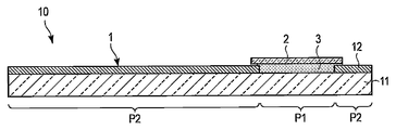
- 2 is a cross-sectional view taken along the line II-II of the forgery prevention medium shown in FIG.
- the anti-counterfeit medium 1 shown in FIGS. 1 and 2 is a banknote such as a bank note.
- the forgery prevention medium 1 may be other securities such as gift certificates.
- the forgery prevention medium 1 may be a certificate such as a passport.
- the anti-counterfeit medium 1 includes a support 1, an anti-counterfeit element 2, and an adhesive layer 3.
- the support 1 is in the form of a film or a sheet.
- the support 1 includes a first part P1 having light transparency and a second part P2 having light shielding properties.
- the first part P1 and the second part P2 are adjacent to each other in a direction parallel to the main surface of the support 1.
- the first portion P1 is circular, and the second portion P2 surrounds the first portion P1.
- the first portion P1 may have a shape other than a circle, and the second portion P2 may not surround the first portion P1.
- the support 1 may include two or more first portions P1 and may include two or more second portions P2.
- the support 1 includes a transparent substrate 11 and a concealing layer 12.
- the transparent base material 11 is a film or a sheet form here.
- the stretched film may be either a uniaxially stretched film or a biaxially stretched film.
- unstretched films and stretched film materials are, for example, cellophane, polycarbonate (PC), polyethylene (PE), polypropylene (PP), polyolefin (PO), ethylene vinyl alcohol (EVOH), polyvinyl alcohol (PVA), poly They are vinyl chloride, polyethylene naphthalate (PEN), polyethylene terephthalate (PET), nylon, acrylic resin, and triacetyl cellulose (TAC).
- the hiding layer 12 covers one main surface of the transparent substrate 11.
- the concealing layer 12 is opened at a position corresponding to the first portion P1.
- the first portion P ⁇ b> 1 is a portion corresponding to the opening of the masking layer 12 in the support 1.
- the second portion P2 is a portion corresponding to the concealment layer 12 in the support 1.
- the concealing layer 12 makes the transmittance or transparency of the second portion P2 smaller than the transmittance or transparency of the first portion P1.
- a printing pattern is provided in the second portion P2.
- the concealing layer 12 prevents the visibility of the other printing pattern from being lowered by one printing pattern.
- the masking layer 12 is a light shielding layer, for example.
- the masking layer 12 can be formed by a known method such as silk screen printing, offset printing, and gravure printing.
- paper or a composite of paper and a resin film may be used as the support 1.
- paper having an opening may be used as the support 1.
- the forgery prevention element 2 faces the support 1 at the position of the first portion P1.
- the forgery prevention element 2 is, for example, a film or a sheet.
- the anti-counterfeit element 2 is light transmissive.
- the anti-counterfeit element 2 is at least partially transparent. The anti-counterfeit element 2 will be described in detail later.
- the adhesive layer 3 is interposed between the support 1 and the anti-counterfeit element 2.
- the adhesive layer 3 has the groove preventing element 2 bonded to the support 1.
- the adhesive layer 3 is light transmissive. Typically, the adhesive layer 3 is transparent.
- the material for the adhesive layer 3 include adhesives such as vinyl chloride-vinyl acetate copolymer, polyester and polyamide, or adhesives such as acrylic, butyl rubber, natural rubber, silicon and polyisobutyl.
- the modifier alone, or an aggregating component such as alkyl methacrylate, vinyl ester, acrylonitrile, styrene and vinyl monomer, and a modifier represented by unsaturated carboxylic acid, hydroxy group-containing monomer, acrylonitrile and the like, It can be used together with additives such as a polymerization initiator, a plasticizer, a curing agent, a curing accelerator and an antioxidant.
- the adhesive layer 3 can be formed by, for example, a known printing method such as a gravure printing method, an offset printing method, or a screen printing method, or a coating method such as a bar coating method, a gravure method, or a roll coating method.
- the adhesive layer 3 may be provided by using an adhesive layer having a film separator on both sides.
- a known method such as roll lamination or thermal transfer can be used for bonding the support 1 and the forgery prevention element 2 together.
- FIG. 3 is a plan view schematically showing the back surface of the anti-counterfeit element included in the anti-counterfeit medium shown in FIG. 4 is a plan view schematically showing the surface of the anti-counterfeiting element shown in FIG.
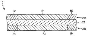
- FIG. 5 is a cross-sectional view taken along line VV of the forgery preventing element shown in FIG.
- the anti-counterfeiting element 2 shown in FIGS. 3 to 5 includes retardation layers 21 a and 21 b and a polarizing layer 22.
- the polarizing layer 22 is interposed between the retardation layers 21a and 21b.
- the forgery prevention element 2 is supported by the support 1 so that the retardation layer 21a faces the first portion P1.
- One of the retardation layers 21a and 21b can be omitted.
- the retardation layer 21a is made of an optically anisotropic material, specifically, a material exhibiting birefringence.
- Birefringence is a phenomenon in which two refracted lights having different velocities are generated when light is incident on a medium having optical anisotropy.
- the retardation layer 21a includes regions R1 and R2 having different slow axis (or optical axis) directions.
- the regions R1 and R2 are adjacent to each other in a direction perpendicular to the thickness direction of the retardation layer 21a.
- Regions R1 and R2 constitute a latent image that is impossible or difficult to distinguish from each other under normal conditions and is visualized under specific conditions.
- the region R1 has a heart shape, and the region R2 surrounds the region R1. Regions R1 and R2 may have other shapes.
- the retardation layer 21a includes regions R1 and R2 having different slow axis directions, but the retardation layer 21a has one or more regions having different slow axis directions from the regions R1 and R2. May further be included.
- each of the regions R1 and R2 has an optical axis substantially parallel to its main surface, and the refractive index in the direction parallel to the optical axis is different from the refractive index in the direction perpendicular to the optical axis. ing. Therefore, for example, when light is incident on the region R1 or R2 perpendicularly, a linearly polarized component whose electric field vector oscillation direction is parallel to the optical axis and a linearly polarized component whose electric field vector oscillation direction is parallel to the optical axis are: Propagating at different velocities, producing a phase difference between them depending on the thickness of the region R1 or R2 and the refractive index difference.
- Each of the regions R1 and R2 may have an arbitrary phase difference between the linearly polarized light whose electric field vector oscillation direction is parallel to the optical axis and the perpendicularly polarized light.
- the phase difference that region R1 causes for these linearly polarized light is equal to the phase difference that region R2 causes for these linearly polarized light.
- the phase difference that the region R1 causes in the linearly polarized light may be different from the phase difference that the region R2 causes in the linearly polarized light.
- the retardation layer 21a can be formed, for example, by applying a liquid crystal material on an alignment film and solidifying the coating film.
- regions R1 and R2 having different slow axis directions are obtained.
- the alignment layer and the retardation layer 21 a may be sequentially formed on the polarizing layer 22, and the adhesive layer, the alignment layer, and the retardation layer 21 a may be sequentially formed on the polarizing layer 22.
- the alignment layer and the retardation layer 21a are sequentially formed on a separately prepared substrate, and the retardation layer 21a is transferred from the substrate onto the polarizing layer 22, or the retardation layer 21a peeled off from the substrate is used as the polarizing layer. 22 may be attached.
- the alignment film is made of, for example, polyimide or polyvinyl alcohol (PVA).
- the alignment film is obtained, for example, by forming a coating film by a known technique such as a gravure coating method and a micro gravure coating method, and subjecting this coating film to an alignment treatment.
- the alignment treatment for example, rubbing treatment or optical alignment treatment can be used.
- rubbing treatment first, a coating film made of a solution containing a polymer such as polyimide and PVA is formed. Next, the coating film is dried, and the surface of the coating film is rubbed with a rubbing cloth. When a liquid crystal material is applied on the alignment film thus obtained, the liquid crystal molecules are aligned in the rubbing direction.
- the rubbing process is performed twice as described below.
- a coating film made of a polymer is formed, and a part of the surface is covered with a mask.
- a rubbing process is performed on the surface of the coating film that is not covered with a mask.
- the mask is removed from the coating film, the rubbing-treated area on the surface of the coating film is covered with a mask, and the other areas are subjected to rubbing treatment.
- a liquid crystal material is applied on the alignment film thus obtained, and the coating film is cured. If the rubbing direction is made different between the first rubbing process and the second rubbing process, regions R1 and R2 having different slow axis directions are obtained.
- photo-alignment treatment for example, photoisomerization of azobenzene derivatives, photodimerization or photocrosslinking of derivatives such as cinnamic acid ester, coumarin, chalcone and benzophenone, or photodecomposition of polyimide or the like is used. Specifically, first, a coating film containing the photosensitive material is formed. Then, this coating film is irradiated with linearly polarized light or irradiated with natural light from an oblique direction. This induces an anisotropic rearrangement or chemical reaction of the molecules in the coating. When a liquid crystal material is applied on the alignment film thus obtained, the liquid crystal molecules are aligned corresponding to the anisotropic arrangement of the molecules in the alignment film.
- the photo-alignment process is performed as described below.
- a coating film containing a photosensitive material is formed, and a part thereof is exposed to linearly polarized light through a photomask.
- the other part of the coating film is exposed to linearly polarized light through a photomask.
- a liquid crystal material is applied on the alignment film thus obtained, and the coating film is cured. If the vibration direction of the electric field vector of linearly polarized light is made different between the first exposure and the second exposure, regions R1 and R2 having different slow axis directions can be obtained.
- a coating film containing a photosensitive material is formed, and a part thereof is exposed with natural light from an oblique direction through a photomask.
- the other part of the coating film is exposed with natural light from an oblique direction through a photomask.
- a liquid crystal material is applied on the alignment film thus obtained, and the coating film is cured. If the irradiation direction of natural light is made different between the first exposure and the second exposure, regions R1 and R2 having different slow axis directions can be obtained.
- the first exposure may be performed on the entire coating film.
- the retardation layer 21a is obtained from a thermotropic liquid crystal such as a smectic liquid crystal or a nematic liquid crystal.
- a polymerizable liquid crystal material that is cured by electron beam or ultraviolet irradiation is applied on the alignment film.
- the polymerizable liquid crystal material include, for example, a mixture containing a main chain monomer containing a reactive functional group such as an acrylic group at both ends of a mesogenic group and a photopolymerization initiator, and a polymerizable functional group at one end of the mesogenic group.
- a mixture containing a side chain monomer and a photopolymerization initiator or a mixture containing a side chain monomer containing a reactive functional group at one end of a mesogenic group, a reactive polymer, and a photopolymerization initiator.
- a gravure coating method or a micro gravure coating method can be used.
- this coating film is irradiated with an electron beam or ultraviolet rays, a retardation layer 21a made of a side-chain or main-chain polymer liquid crystal is obtained.
- the coating film Before the irradiation with the electron beam or the ultraviolet ray, the coating film may be heat-treated at a temperature slightly lower than the phase transition point (NI point) between the nematic phase and the isotropic phase. In this way, the orientation of the mesogenic group can be promoted.
- NI point phase transition point
- the alignment film There are layers of birefringence in the alignment film. Such a layer may be used as the retardation layer 21a. In this case, the alignment film can be omitted.
- the retardation layer 21b faces the retardation layer 21a with the polarizing layer 22 interposed therebetween.
- the retardation layer 21b is made of an optically anisotropic material, specifically, a material exhibiting birefringence.
- the retardation layer 21b includes regions R3 and R4 having different slow axis (or optical axis) directions.
- the regions R3 and R4 are adjacent to each other in a direction perpendicular to the thickness direction of the retardation layer 21b.
- Regions R3 and R4 constitute a latent image that is impossible or difficult to distinguish from each other under normal conditions and is visualized under specific conditions.
- the region R3 has a star shape, and the region R4 surrounds the region R3. Regions R3 and R4 may have other shapes. Further, here, the retardation layer 21b includes regions R3 and R4 having different slow axis directions, but the retardation layer 21b has one or more regions having different slow axis directions from the regions R3 and R4. May further be included.
- the pattern of the region included in the retardation layer 21b is different from the pattern of the region included in the retardation layer 21b.
- different images can be displayed on the anti-counterfeit element 2 depending on whether the anti-counterfeit medium 10 is observed from the front side or the rear side.
- each of the regions R3 and R4 has an optical axis substantially parallel to its main surface, and the refractive index in the direction parallel to the optical axis is different from the refractive index in the direction perpendicular to the optical axis. ing. Therefore, for example, when light is incident perpendicular to the region R3 or R4, a linearly polarized component whose electric field vector oscillation direction is parallel to the optical axis and a linearly polarized component whose electric field vector oscillation direction is parallel to the optical axis are: Propagating at different velocities, producing a phase difference between them depending on the thickness of the region R3 or R4 and the refractive index difference.
- the angle formed by the optical axis of the region R3 and the optical axis of the region R4 may be the same as or different from the angle formed by the optical axis of the region R1 and the optical axis of the region R2.
- Each optical axis of the regions R3 and R4 may be parallel or perpendicular to at least one of the optical axes of the regions R1 and R2, or may be oblique.
- Each of the regions R3 and R4 may have an arbitrary phase difference between the linearly polarized light whose electric field vector oscillation direction is parallel to the optical axis and the perpendicularly polarized light.
- the phase difference that region R3 causes for these linearly polarized light is equal to the phase difference that region R4 causes for these linearly polarized light.
- the phase difference that the region R3 causes in the linearly polarized light may be different from the phase difference that the region R4 causes in the linearly polarized light.
- the phase difference generated in the linearly polarized light by the region R3 or R4 may be the same as or different from the phase difference generated in the linearly polarized light by the region R1 or R2.
- all of the regions R1 to R4 may serve as a half-wave plate for light of the same wavelength, and all of the regions R1 to R4 may serve as a quarter-wave plate for light of the same wavelength. You may play a role.
- the regions R1 and R2 may serve as a half-wave plate for light of the same wavelength, and the regions R3 and R4 may serve as a quarter-wave plate for light of the previous wavelength. Good.
- the polarizing layer 22 is interposed between the retardation layers 21a and 21b.
- the polarizing layer 22 faces the first portion P1 with the retardation layer 21b interposed therebetween.
- the polarizing layer 22 is a linear polarizer, for example, an absorption linear polarizer.
- a polarizer obtained by impregnating a PVA film with iodine or a dichroic dye and stretching it, or a polarizer obtained by orienting a dichroic dye on an alignment film is used. Can be used.
- FIG. 6 schematically shows an image displayed by the forgery prevention element when the forgery prevention medium is observed with the naked eye from the surface side in the first state in which no reflector is present behind the forgery prevention medium shown in FIG.
- FIG. 7 schematically shows an image displayed by the anti-counterfeit element when the anti-counterfeit medium is observed with the naked eye from the surface side in the second state where the reflector exists behind the anti-counterfeit medium shown in FIG.
- FIG. 8 schematically shows an image displayed by the anti-counterfeit element when the anti-counterfeit medium is observed with the naked eye from the back side in the second state where the reflector exists behind the anti-counterfeit medium shown in FIG.
- the main surface on which the anti-counterfeiting element 2 is provided is the front surface, and the opposite surface is the back surface.
- the term “behind” is used to express the position of the reflector relative to the observer.
- Each of the regions R1 to R4 serves as a quarter-wave plate for a specific wavelength in the visible range.
- the polarizing layer 22 is an absorption linear polarizer.
- the slow axes of the regions R1 and R4 are parallel or perpendicular to the transmission axis of the polarizing layer 22, and the slow axes of the regions R2 and R3 form an angle of 45 ° with respect to the transmission axis of the polarizing layer 22.
- the coin 5 is not present here
- the anti-counterfeit medium 10 is observed with the naked eye from the surface side, it is impossible or difficult to distinguish the regions R1 and R2 from each other, and it is impossible or difficult to distinguish the regions R3 and R4 from each other. Therefore, in this case, the forgery prevention element 2 looks like a transparent layer. In this state, even if the anti-counterfeit medium 10 is turned over, the anti-counterfeit element 2 looks like a transparent layer.
- linearly polarized light the component incident on the region R1 is emitted from the region R1 as linearly polarized light.
- the linearly polarized light is reflected by the coin 5, and then passes through the retardation layer 21a, the polarizing layer 22, and the retardation layer 21b, and reaches the observer.
- the component incident on the region R2 is emitted from the region R2 as right or left circularly polarized light.
- the right or left circularly polarized light is converted into left or right circularly polarized light by being reflected by the coin 5.
- the left or right circularly polarized light passes through the region R ⁇ b> 2, and is converted into linearly polarized light in which the vibration direction of the electric field vector is perpendicular to the transmission axis of the polarizing layer 22. Therefore, this linearly polarized light is absorbed by the polarizing layer 22 and does not reach the observer.
- the forgery prevention medium 10 displays an image I1 shown in FIG. 7 at the position of the forgery prevention element 2.
- linearly polarized light the component incident on the region R4 is emitted from the region R4 as linearly polarized light.
- the linearly polarized light is reflected by the coin 5, and then passes through the retardation layer 21b, the polarizing layer 22, and the retardation layer 21a, and reaches the observer.
- the component incident on the region R3 is emitted from the region R3 as right or left circularly polarized light.
- the right or left circularly polarized light is converted into left or right circularly polarized light by being reflected by the coin 5.
- the left or right circularly polarized light passes through the region R ⁇ b> 3, and is converted into linearly polarized light in which the vibration direction of the electric field vector is perpendicular to the transmission axis of the polarizing layer 22. Therefore, this linearly polarized light is absorbed by the polarizing layer 22 and does not reach the observer.
- the forgery prevention medium 10 displays the image I2 shown in FIG. 8 at the position of the forgery prevention element 2.
- the forgery prevention medium 10 displays different images I1 and I2 in the second state. In the first state, these images I1 and I2 cannot be observed. And it is difficult to realize that a reflector is required to visualize these latent images. In other words, it is difficult for the forgery prevention medium 10 to realize the forgery prevention technology employed. Moreover, it is easy for a person who knows that a reflector is necessary for visualizing the latent image to make a true / false determination using the images I1 and / or I2.
- this anti-counterfeit medium 10 may display images I1 and / or I2 without a reflector.
- some liquid crystal displays emit linearly polarized light or elliptically polarized light as display light.
- the anti-counterfeit medium 10 displays the image I1 or I2 at the position of the anti-counterfeit element 2.
- polarized light in nature.
- natural light may become elliptically polarized light when reflected from the surface of water or plastic. If it is known that such light is polarized light, the image I1 or I2 can be displayed on the anti-counterfeit medium 10 using the polarized light.
- a light scattering layer may be provided on at least one of the retardation layers 21a and 21b in order to prevent the image I1 or I2 from being displayed under a normal environment.
- the light scattering layer may be provided so as to face the polarizing layer 22 with the retardation layer 21a interposed therebetween.
- the light scattering layer may be provided so as to face the polarizing layer 22 with the retardation layer 21b interposed therebetween.
- the first light scattering layer is provided so as to face the polarizing layer 22 with the retardation layer 21a interposed therebetween, and the second light scattering layer is provided so as to face the polarizing layer 22 with the retardation layer 21b interposed therebetween. Also good.
- the light scattering layer is, for example, a light transmissive layer having a fine uneven structure on the surface.
- a light scattering layer is obtained from, for example, a mixture of a light-transmitting resin and a filler, and has an irregularity with an arithmetic average roughness Ra of about 2 ⁇ m as defined in Japanese Industrial Standards JIS B 0601-2001. Form.
- the light scattering layer having such a structure is provided on the retardation layer 21b, for example.
- the light scattering layer a layer whose light scattering ability is mainly caused by internal scattering may be used.
- a light scattering layer is obtained, for example, from a mixture of a light-transmitting resin and a filler having a different refractive index.
- the light scattering layer having such a structure is provided on the retardation layer 21a and / or 21b, for example.
- the refractive index difference ⁇ n between the light-transmitting resin and the filler is preferably 0.03 ⁇ ⁇ n ⁇ 0.3.
- the difference in refractive index is small, a large amount of filler is required to obtain the effect of internal scattering, and the light scattering layer may become brittle.
- the difference in refractive index is large, the amount of filler needs to be small to achieve an appropriate light scattering ability, and there is a possibility that uniform internal scattering cannot be obtained.
- the average particle diameter d of the filler is, for example, 0.01 ⁇ m ⁇ d ⁇ 5 ⁇ m. When the average particle diameter d is small, it may be difficult to uniformly disperse the filler. When the average particle diameter d is large, the effect of the internal scattering layer may be reduced.
- the haze value Hz of the light scattering layer is, for example, 2 ⁇ Hz ⁇ 10. In this case, it is possible to prevent the latent image from being visualized by polarized light generated in a normal environment.
- the light scattering layer can serve as a protective layer.
- a protective layer may be provided on the anti-counterfeit medium 10 and the protective layer may serve as a light scattering layer.
- the adhesive layer 3 may serve as a light scattering layer.
- Examples of light-transmitting resins include acrylic resins, epoxy resins, polyester resins, urethane resins; copolymers thereof such as acrylic silicon resins; and toughness by adding curing agents such as isocyanates and epoxides to these resins. Or a compound having a (meth) acryloyl group in the molecule, particularly a compound having 1 to 20 (meth) acryloyl groups.
- resins such as trimethylolpropane tri (meth) acrylate, pentaerythritol tri (meth) acrylate, pentaerythritol tetra (meth) acrylate, and dipentaerythritol hexa (meth) acrylate, and active energy rays such as ultraviolet rays.
- active energy rays such as ultraviolet rays.
- produces a radical by irradiating is mentioned.
- the material mentioned above about the contact bonding layer 3 can also be used as light transmissive resin.
- a filler made of a resin such as a styrene resin, a melamine resin, an acrylic styrene resin, a polycarbonate resin, or a polyethylene resin can be used.
- a filler you may use the filler which consists of clay minerals, such as an inorganic substance, for example, a silica, a titanium oxide, and a talc.
- a dispersion liquid containing a light transmitting resin and a filler is obtained.
- a solvent is used as necessary.
- a coating film made of the previous dispersion is formed using a printing method such as a gravure printing method, an offset printing method and a screen printing method, or a coating method such as a bar coating method, a gravure method and a roll coating method. Dry the membrane.
- active energy rays such as ultraviolet rays.
- a protective layer may be provided on the surface of the anti-counterfeit medium 10 for the purpose of protecting the support 1 and / or the anti-counterfeit element 2 from physical or chemical damage. As described above, this protective layer may serve as a light scattering layer.
- the forgery prevention medium 10 is usually provided with a printing pattern.
- the print pattern is provided so as not to disturb the visibility of the images I1 and I2.
- the anti-counterfeit medium 10 may be provided with a relief type diffractive structure such as a hologram and a diffraction grating. By adopting this structure, a higher forgery prevention effect can be achieved.
- the anti-counterfeiting element 2 may be composed of two parts, one part may be supported on the surface of the support 11, and the other part may be supported on the back surface of the support 11. That is, the retardation layer 21a and the polarizing layer 22 may face each other with the support 11 interposed therebetween. Alternatively, the retardation layer 21b and the polarizing layer 22 may face each other with the support 11 interposed therebetween.
- Example> The anti-counterfeit medium 10 described with reference to FIGS. 1 to 5 was manufactured by the following method.
- a PVA-iodine film obtained by impregnating iodine in a PVA stretched film was prepared.
- a 10 wt% solution of polyvinyl alcohol was applied to one main surface of the polarizing layer 22 using a bar coater so that the dry film thickness was 2 ⁇ m.
- PVA-117 manufactured by Kuraray Co., Ltd. was used as the polyvinyl alcohol.
- a first mask opened in the same shape as the region R1 was placed on the coating film, and in this state, the coating film was rubbed.
- FINE PUFF YA-20-R manufactured by Yoshikawa Chemical Co., Ltd. was used as the rubbing cloth. The rubbing direction was made to coincide with the transmission axis of the polarizing layer 22.
- a second mask having the same shape as the region R1 was placed on the coating film so that the entire region subjected to the rubbing treatment was covered with the second mask.
- the coating film was rubbed.
- FINE PUFF YA-20-R manufactured by Yoshikawa Chemical Co., Ltd. was used as the rubbing cloth.
- the angle formed by the rubbing direction and the transmission axis of the polarizing layer 22 was 45 °. As described above, an alignment film was formed on the polarizing layer 22.
- the following liquid crystal solution was gravure-printed on this alignment film.
- the film thus obtained was dried at 100 ° C. for 1 minute. Subsequently, the dried film was irradiated with ultraviolet rays with an irradiation energy of 500 mJ using a high-pressure mercury lamp in a nitrogen atmosphere. Thus, a retardation layer 21a having a thickness of about 1 ⁇ m was obtained.
- PASF color LC242 manufactured by BASF
- polymerization initiator Irgacure 184, manufactured by Ciba Geigy
- Solvent 68.5 parts by mass (mixture containing toluene and methyl ethyl ketone in the same mass)
- a 10 wt% solution of polyvinyl alcohol was applied to the other main surface of the polarizing layer 22 using a bar coater so that the dry film thickness was 2 ⁇ m.
- PVA-117 manufactured by Kuraray Co., Ltd. was used as the polyvinyl alcohol.
- a third mask having the same shape as the region R3 was placed on the coating film, and in this state, the coating film was rubbed.
- FINE PUFF YA-20-R manufactured by Yoshikawa Chemical Co., Ltd. was used as the rubbing cloth. The rubbing direction was made to coincide with the transmission axis of the polarizing layer 22.
- a fourth mask opened in the same shape as the region R3 was placed on the coating film so that the entire region subjected to the rubbing treatment was covered with the fourth mask.
- the coating film was rubbed.
- FINE PUFF YA-20-R manufactured by Yoshikawa Chemical Co., Ltd. was used as the rubbing cloth.
- the angle formed by the rubbing direction and the transmission axis of the polarizing layer 22 was 45 °. As described above, an alignment film was formed on the polarizing layer 22.
- the liquid crystal solution was subjected to gravure printing on the alignment film.
- the film thus obtained was dried at 100 ° C. for 1 minute.
- the dried film was irradiated with ultraviolet rays with an irradiation energy of 500 mJ using a high-pressure mercury lamp in a nitrogen atmosphere.
- a retardation layer 21b having a thickness of about 1 ⁇ m was obtained.
- the forgery prevention element 2 was completed.
- a TAC film having a thickness of 40 ⁇ m was prepared as the transparent substrate 11.
- silk screen ink fountain SS8-611 white manufactured by Toyo Ink Manufacturing Co., Ltd. was screen-printed to form a concealing layer 12 having an opening corresponding to the anti-counterfeiting element 2. Thereby, the base material 1 was obtained.
- the base material 11 and the forgery prevention element 2 were bonded together through the adhesive layer 3. As described above, the forgery prevention medium 10 was completed.
- the anti-counterfeit medium 10 was observed with the naked eye while illuminating with natural light without placing a reflector behind it. As a result, the whole forgery prevention element 2 appeared to be a transparent gray color.
- the surface of the anti-counterfeit medium 10 was observed with the naked eye while the coin 5 was positioned behind it and illuminated with natural light.
- the forgery prevention element 2 displayed an image I1 shown in FIG.
- the back surface of the forgery prevention medium 10 was observed with the naked eye while the coin 5 was positioned behind the medium and illuminated with natural light.
- the forgery prevention element 2 displayed an image I2 shown in FIG.
Landscapes
- Physics & Mathematics (AREA)
- Business, Economics & Management (AREA)
- Accounting & Taxation (AREA)
- Finance (AREA)
- General Physics & Mathematics (AREA)
- Optics & Photonics (AREA)
- Chemical & Material Sciences (AREA)
- Crystallography & Structural Chemistry (AREA)
- Engineering & Computer Science (AREA)
- Manufacturing & Machinery (AREA)
- Polarising Elements (AREA)
- Credit Cards Or The Like (AREA)
- Printing Methods (AREA)
- Inspection Of Paper Currency And Valuable Securities (AREA)
Abstract
Selon cette invention, il est possible de vérifier facilement l'authenticité d'un support protégé contre la contrefaçon (10) qui est fabriqué à un faible coût. Ce support protégé contre la contrefaçon (10) comprend une base (1) qui comporte une portion (P1) présentant des propriétés de transmission de lumière, une couche à différence de phase (2) opposée à la portion (P1) et comprenant une pluralité de régions (R1, R2) présentant mutuellement différentes directions à axe lent, et une couche polarisée (3) opposée à la couche à différence de phase (2) au niveau de la position de la portion (P1). Ce support protégé contre la contrefaçon (10) comprend comme polariseur uniquement la couche polarisée (3). Cette portion du support protégé contre la contrefaçon (10), la portion (P1), la couche à différence de phase (2) et la couche polarisée (3) formant une structure stratifiée, présente des propriétés de transmission de lumière.
Priority Applications (6)
| Application Number | Priority Date | Filing Date | Title |
|---|---|---|---|
| EP19164585.2A EP3537191B1 (fr) | 2011-02-28 | 2012-02-27 | Procédé de vérification d'un support anticontrefaçon |
| EP12752008.8A EP2682791B1 (fr) | 2011-02-28 | 2012-02-27 | Support protégé contre la contrefaçon et procédé de vérification |
| AU2012224134A AU2012224134B2 (en) | 2011-02-28 | 2012-02-27 | Forgery-proof medium and verification method |
| US14/012,651 US10189293B2 (en) | 2011-02-28 | 2013-08-28 | Anti-counterfeit medium and verification method |
| AU2016201176A AU2016201176C1 (en) | 2011-02-28 | 2016-02-25 | Forgery-proof medium and verification method |
| AU2016201177A AU2016201177B2 (en) | 2011-02-28 | 2016-02-25 | Forgery-proof medium and verification method |
Applications Claiming Priority (2)
| Application Number | Priority Date | Filing Date | Title |
|---|---|---|---|
| JP2011041609A JP5736840B2 (ja) | 2011-02-28 | 2011-02-28 | 偽造防止媒体 |
| JP2011-041609 | 2011-02-28 |
Related Child Applications (1)
| Application Number | Title | Priority Date | Filing Date |
|---|---|---|---|
| US14/012,651 Continuation US10189293B2 (en) | 2011-02-28 | 2013-08-28 | Anti-counterfeit medium and verification method |
Publications (1)
| Publication Number | Publication Date |
|---|---|
| WO2012118013A1 true WO2012118013A1 (fr) | 2012-09-07 |
Family
ID=46757947
Family Applications (1)
| Application Number | Title | Priority Date | Filing Date |
|---|---|---|---|
| PCT/JP2012/054785 Ceased WO2012118013A1 (fr) | 2011-02-28 | 2012-02-27 | Support protégé contre la contrefaçon et procédé de vérification |
Country Status (5)
| Country | Link |
|---|---|
| US (1) | US10189293B2 (fr) |
| EP (2) | EP3537191B1 (fr) |
| JP (1) | JP5736840B2 (fr) |
| AU (3) | AU2012224134B2 (fr) |
| WO (1) | WO2012118013A1 (fr) |
Cited By (2)
| Publication number | Priority date | Publication date | Assignee | Title |
|---|---|---|---|---|
| JP2014062983A (ja) * | 2012-09-20 | 2014-04-10 | Toppan Printing Co Ltd | 表示体及びラベル付き物品 |
| WO2020004155A1 (fr) * | 2018-06-29 | 2020-01-02 | 日本ゼオン株式会社 | Support d'identification, procédé de détermination d'authenticité et article associé |
Families Citing this family (15)
| Publication number | Priority date | Publication date | Assignee | Title |
|---|---|---|---|---|
| JP5736840B2 (ja) | 2011-02-28 | 2015-06-17 | 凸版印刷株式会社 | 偽造防止媒体 |
| KR102329698B1 (ko) * | 2013-08-09 | 2021-11-23 | 스미또모 가가꾸 가부시키가이샤 | 장척 원편광판의 제조 방법 및 장척 원편광판 |
| JP6318677B2 (ja) * | 2014-02-17 | 2018-05-09 | 凸版印刷株式会社 | 配向膜の製造方法、および、表示体の製造方法 |
| WO2015129706A1 (fr) * | 2014-02-26 | 2015-09-03 | 富士フイルム株式会社 | Plaque de polarisation et dispositif d'affichage d'image |
| JP2016009082A (ja) * | 2014-06-24 | 2016-01-18 | 大日本印刷株式会社 | 真偽判定具 |
| JP6511742B2 (ja) * | 2014-07-17 | 2019-05-15 | 大日本印刷株式会社 | 真偽判定具 |
| CN107660273B (zh) * | 2015-05-26 | 2021-10-22 | 罗利克有限公司 | 光学安全装置 |
| WO2016188936A1 (fr) * | 2015-05-26 | 2016-12-01 | Rolic Ag | Dispositif de sécurité comportant plusieurs images cachées |
| US10800202B2 (en) * | 2015-07-10 | 2020-10-13 | Universidad Politecnica De Madrid | Method and device for document security by generating multiple reflective and transmissive latent images |
| EP3896501B1 (fr) * | 2018-12-11 | 2025-03-26 | Zeon Corporation | Visionneuse de détermination d'authenticité et son procédé de fabrication, procédé pour déterminer l'authenticité d'un support d'authentification et ensemble de détermination d'authenticité |
| WO2020156657A1 (fr) * | 2019-01-30 | 2020-08-06 | Kba-Notasys Sa | Procédé de préparation d'articles de sécurité polymères |
| CN113677538B (zh) * | 2019-01-30 | 2023-09-19 | 柯尼格及包尔纸币解决方案有限公司 | 用于制备聚合物安全制品的工艺 |
| WO2020156656A1 (fr) | 2019-01-30 | 2020-08-06 | Kba-Notasys Sa | Procédé de préparation d'articles de sécurité polymères |
| EA035961B1 (ru) * | 2019-06-28 | 2020-09-07 | Закрытое Акционерное Общество "Голографическая Индустрия" | Способ изготовления прозрачных вставок для защиты от подделок идентификационных карт и поликарбонатных листов биометрических паспортов |
| CN112866906A (zh) * | 2021-02-09 | 2021-05-28 | 珠海格力电器股份有限公司 | 一种设备激活方法、服务器、设备及系统 |
Citations (4)
| Publication number | Priority date | Publication date | Assignee | Title |
|---|---|---|---|---|
| JP2001525080A (ja) | 1997-05-09 | 2001-12-04 | ロリク アーゲー | 光学素子 |
| JP2005326882A (ja) | 1994-06-24 | 2005-11-24 | Rolic Ag | 液晶異方性層を有する層状光学的構成部品 |
| JP2009073103A (ja) * | 2007-09-21 | 2009-04-09 | Toppan Printing Co Ltd | 情報記録媒体及び情報読取装置 |
| JP2010280079A (ja) * | 2009-06-02 | 2010-12-16 | Toppan Printing Co Ltd | 表示体、粘着ラベル、転写箔及びラベル付き物品 |
Family Cites Families (5)
| Publication number | Priority date | Publication date | Assignee | Title |
|---|---|---|---|---|
| US20040120040A1 (en) * | 1998-11-13 | 2004-06-24 | Rolic Ag | Optical component |
| EP1120737A1 (fr) * | 2000-01-27 | 2001-08-01 | Rolic AG | Dispositif optique de sécurité |
| JP4935328B2 (ja) * | 2006-11-30 | 2012-05-23 | 凸版印刷株式会社 | 積層体、粘着ラベル、記録媒体、ラベル付き物品、検証具、キット及び判別方法 |
| DE102007007914A1 (de) * | 2007-02-14 | 2008-08-21 | Giesecke & Devrient Gmbh | Prägelack für mikrooptische Sicherheitselemente |
| JP5736840B2 (ja) | 2011-02-28 | 2015-06-17 | 凸版印刷株式会社 | 偽造防止媒体 |
-
2011
- 2011-02-28 JP JP2011041609A patent/JP5736840B2/ja not_active Expired - Fee Related
-
2012
- 2012-02-27 EP EP19164585.2A patent/EP3537191B1/fr active Active
- 2012-02-27 WO PCT/JP2012/054785 patent/WO2012118013A1/fr not_active Ceased
- 2012-02-27 AU AU2012224134A patent/AU2012224134B2/en not_active Ceased
- 2012-02-27 EP EP12752008.8A patent/EP2682791B1/fr active Active
-
2013
- 2013-08-28 US US14/012,651 patent/US10189293B2/en active Active
-
2016
- 2016-02-25 AU AU2016201176A patent/AU2016201176C1/en active Active
- 2016-02-25 AU AU2016201177A patent/AU2016201177B2/en active Active
Patent Citations (4)
| Publication number | Priority date | Publication date | Assignee | Title |
|---|---|---|---|---|
| JP2005326882A (ja) | 1994-06-24 | 2005-11-24 | Rolic Ag | 液晶異方性層を有する層状光学的構成部品 |
| JP2001525080A (ja) | 1997-05-09 | 2001-12-04 | ロリク アーゲー | 光学素子 |
| JP2009073103A (ja) * | 2007-09-21 | 2009-04-09 | Toppan Printing Co Ltd | 情報記録媒体及び情報読取装置 |
| JP2010280079A (ja) * | 2009-06-02 | 2010-12-16 | Toppan Printing Co Ltd | 表示体、粘着ラベル、転写箔及びラベル付き物品 |
Cited By (7)
| Publication number | Priority date | Publication date | Assignee | Title |
|---|---|---|---|---|
| JP2014062983A (ja) * | 2012-09-20 | 2014-04-10 | Toppan Printing Co Ltd | 表示体及びラベル付き物品 |
| WO2020004155A1 (fr) * | 2018-06-29 | 2020-01-02 | 日本ゼオン株式会社 | Support d'identification, procédé de détermination d'authenticité et article associé |
| CN112368613A (zh) * | 2018-06-29 | 2021-02-12 | 日本瑞翁株式会社 | 识别介质、真实性判定方法以及物品 |
| JPWO2020004155A1 (ja) * | 2018-06-29 | 2021-08-05 | 日本ゼオン株式会社 | 識別媒体、真正性判定方法、及び物品 |
| CN112368613B (zh) * | 2018-06-29 | 2022-10-21 | 日本瑞翁株式会社 | 识别介质、真实性判定方法以及物品 |
| JP7396275B2 (ja) | 2018-06-29 | 2023-12-12 | 日本ゼオン株式会社 | 識別媒体、真正性判定方法、及び物品 |
| US11975557B2 (en) | 2018-06-29 | 2024-05-07 | Zeon Corporation | Identification medium, authenticity determination method, and article |
Also Published As
| Publication number | Publication date |
|---|---|
| AU2012224134A1 (en) | 2013-10-03 |
| US10189293B2 (en) | 2019-01-29 |
| US20130341903A1 (en) | 2013-12-26 |
| AU2012224134B2 (en) | 2015-11-26 |
| EP2682791A4 (fr) | 2016-07-06 |
| AU2016201176B2 (en) | 2017-08-17 |
| AU2016201176C1 (en) | 2017-11-23 |
| JP5736840B2 (ja) | 2015-06-17 |
| AU2016201177A1 (en) | 2016-03-17 |
| JP2012177842A (ja) | 2012-09-13 |
| EP2682791B1 (fr) | 2019-05-01 |
| EP3537191B1 (fr) | 2020-12-16 |
| AU2016201176A1 (en) | 2016-03-17 |
| EP2682791A1 (fr) | 2014-01-08 |
| AU2016201177B2 (en) | 2017-06-08 |
| EP3537191A1 (fr) | 2019-09-11 |
Similar Documents
| Publication | Publication Date | Title |
|---|---|---|
| AU2016201176B2 (en) | Forgery-proof medium and verification method | |
| JP5597940B2 (ja) | 表示体、粘着ラベル、転写箔及びラベル付き物品 | |
| US10670924B2 (en) | Display and method of manufacturing display | |
| JP5381023B2 (ja) | 画像形成体 | |
| JP2011115974A (ja) | 偽造防止媒体 | |
| JP6179086B2 (ja) | 偽造防止媒体、それを用いた偽造防止ステッカーおよび偽造防止物品 | |
| JP2011221228A (ja) | 偽造防止シールおよび偽造防止シール製造方法 | |
| JP2013109129A (ja) | 偽造防止用表示体、その貼着ラベル、転写箔及び真偽判定方法 | |
| JP5516065B2 (ja) | 真偽判定方法 | |
| JP2008139510A (ja) | 積層体、粘着ラベル、記録媒体、ラベル付き物品及び判別方法 | |
| JP5423031B2 (ja) | 光学素子 | |
| JP5842495B2 (ja) | 情報記録媒体 | |
| JP2008070807A (ja) | 偽造防止媒体、偽造防止ラベル、印刷物、転写箔、および判別方法 | |
| JP5811568B2 (ja) | 偽造防止媒体 | |
| JP5310984B2 (ja) | 可とう性を有する偽造防止用媒体及びその検証方法 | |
| JP5310983B2 (ja) | 可とう性を有する偽造防止用媒体及びその検証方法 | |
| JP5834683B2 (ja) | 偽造防止媒体及びその真贋判定方法並びに偽造防止媒体の製造方法 | |
| JP5696506B2 (ja) | 偽造防止媒体及びその真贋判定方法並びに偽造防止媒体の製造方法 | |
| JP2008139509A (ja) | 積層体、粘着ラベル、記録媒体、ラベル付き物品及び判別方法 | |
| JP2009139766A (ja) | 偏光潜像積層体および媒体 | |
| JP5028642B2 (ja) | 積層体、粘着ラベル、記録媒体、ラベル付き物品及び判別方法 | |
| JP5779985B2 (ja) | 真贋判定用の積層体 | |
| JP2009150969A (ja) | 偽造防止媒体および偽造防止シール |
Legal Events
| Date | Code | Title | Description |
|---|---|---|---|
| 121 | Ep: the epo has been informed by wipo that ep was designated in this application |
Ref document number: 12752008 Country of ref document: EP Kind code of ref document: A1 |
|
| NENP | Non-entry into the national phase |
Ref country code: DE |
|
| ENP | Entry into the national phase |
Ref document number: 2012224134 Country of ref document: AU Date of ref document: 20120227 Kind code of ref document: A |