WO2012121067A1 - Procédé de fabrication de structure d'électrode ayant une longueur d'espace nanoscopique, structure d'électrode ayant une longueur d'espace nanoscopique ainsi obtenue, et nanodispositif - Google Patents
Procédé de fabrication de structure d'électrode ayant une longueur d'espace nanoscopique, structure d'électrode ayant une longueur d'espace nanoscopique ainsi obtenue, et nanodispositif Download PDFInfo
- Publication number
- WO2012121067A1 WO2012121067A1 PCT/JP2012/055002 JP2012055002W WO2012121067A1 WO 2012121067 A1 WO2012121067 A1 WO 2012121067A1 JP 2012055002 W JP2012055002 W JP 2012055002W WO 2012121067 A1 WO2012121067 A1 WO 2012121067A1
- Authority
- WO
- WIPO (PCT)
- Prior art keywords
- electrode
- nanogap
- length
- gap
- metal
- Prior art date
- Legal status (The legal status is an assumption and is not a legal conclusion. Google has not performed a legal analysis and makes no representation as to the accuracy of the status listed.)
- Ceased
Links
Images













Classifications
-
- B—PERFORMING OPERATIONS; TRANSPORTING
- B82—NANOTECHNOLOGY
- B82B—NANOSTRUCTURES FORMED BY MANIPULATION OF INDIVIDUAL ATOMS, MOLECULES, OR LIMITED COLLECTIONS OF ATOMS OR MOLECULES AS DISCRETE UNITS; MANUFACTURE OR TREATMENT THEREOF
- B82B1/00—Nanostructures formed by manipulation of individual atoms or molecules, or limited collections of atoms or molecules as discrete units
-
- B—PERFORMING OPERATIONS; TRANSPORTING
- B82—NANOTECHNOLOGY
- B82B—NANOSTRUCTURES FORMED BY MANIPULATION OF INDIVIDUAL ATOMS, MOLECULES, OR LIMITED COLLECTIONS OF ATOMS OR MOLECULES AS DISCRETE UNITS; MANUFACTURE OR TREATMENT THEREOF
- B82B3/00—Manufacture or treatment of nanostructures by manipulation of individual atoms or molecules, or limited collections of atoms or molecules as discrete units
-
- B—PERFORMING OPERATIONS; TRANSPORTING
- B82—NANOTECHNOLOGY
- B82Y—SPECIFIC USES OR APPLICATIONS OF NANOSTRUCTURES; MEASUREMENT OR ANALYSIS OF NANOSTRUCTURES; MANUFACTURE OR TREATMENT OF NANOSTRUCTURES
- B82Y10/00—Nanotechnology for information processing, storage or transmission, e.g. quantum computing or single electron logic
-
- B—PERFORMING OPERATIONS; TRANSPORTING
- B82—NANOTECHNOLOGY
- B82Y—SPECIFIC USES OR APPLICATIONS OF NANOSTRUCTURES; MEASUREMENT OR ANALYSIS OF NANOSTRUCTURES; MANUFACTURE OR TREATMENT OF NANOSTRUCTURES
- B82Y40/00—Manufacture or treatment of nanostructures
-
- C—CHEMISTRY; METALLURGY
- C23—COATING METALLIC MATERIAL; COATING MATERIAL WITH METALLIC MATERIAL; CHEMICAL SURFACE TREATMENT; DIFFUSION TREATMENT OF METALLIC MATERIAL; COATING BY VACUUM EVAPORATION, BY SPUTTERING, BY ION IMPLANTATION OR BY CHEMICAL VAPOUR DEPOSITION, IN GENERAL; INHIBITING CORROSION OF METALLIC MATERIAL OR INCRUSTATION IN GENERAL
- C23C—COATING METALLIC MATERIAL; COATING MATERIAL WITH METALLIC MATERIAL; SURFACE TREATMENT OF METALLIC MATERIAL BY DIFFUSION INTO THE SURFACE, BY CHEMICAL CONVERSION OR SUBSTITUTION; COATING BY VACUUM EVAPORATION, BY SPUTTERING, BY ION IMPLANTATION OR BY CHEMICAL VAPOUR DEPOSITION, IN GENERAL
- C23C18/00—Chemical coating by decomposition of either liquid compounds or solutions of the coating forming compounds, without leaving reaction products of surface material in the coating; Contact plating
- C23C18/16—Chemical coating by decomposition of either liquid compounds or solutions of the coating forming compounds, without leaving reaction products of surface material in the coating; Contact plating by reduction or substitution, e.g. electroless plating
- C23C18/1601—Process or apparatus
- C23C18/1603—Process or apparatus coating on selected surface areas
- C23C18/1607—Process or apparatus coating on selected surface areas by direct patterning
-
- C—CHEMISTRY; METALLURGY
- C23—COATING METALLIC MATERIAL; COATING MATERIAL WITH METALLIC MATERIAL; CHEMICAL SURFACE TREATMENT; DIFFUSION TREATMENT OF METALLIC MATERIAL; COATING BY VACUUM EVAPORATION, BY SPUTTERING, BY ION IMPLANTATION OR BY CHEMICAL VAPOUR DEPOSITION, IN GENERAL; INHIBITING CORROSION OF METALLIC MATERIAL OR INCRUSTATION IN GENERAL
- C23C—COATING METALLIC MATERIAL; COATING MATERIAL WITH METALLIC MATERIAL; SURFACE TREATMENT OF METALLIC MATERIAL BY DIFFUSION INTO THE SURFACE, BY CHEMICAL CONVERSION OR SUBSTITUTION; COATING BY VACUUM EVAPORATION, BY SPUTTERING, BY ION IMPLANTATION OR BY CHEMICAL VAPOUR DEPOSITION, IN GENERAL
- C23C18/00—Chemical coating by decomposition of either liquid compounds or solutions of the coating forming compounds, without leaving reaction products of surface material in the coating; Contact plating
- C23C18/16—Chemical coating by decomposition of either liquid compounds or solutions of the coating forming compounds, without leaving reaction products of surface material in the coating; Contact plating by reduction or substitution, e.g. electroless plating
- C23C18/1601—Process or apparatus
- C23C18/1603—Process or apparatus coating on selected surface areas
- C23C18/1607—Process or apparatus coating on selected surface areas by direct patterning
- C23C18/161—Process or apparatus coating on selected surface areas by direct patterning from plating step, e.g. inkjet
-
- C—CHEMISTRY; METALLURGY
- C23—COATING METALLIC MATERIAL; COATING MATERIAL WITH METALLIC MATERIAL; CHEMICAL SURFACE TREATMENT; DIFFUSION TREATMENT OF METALLIC MATERIAL; COATING BY VACUUM EVAPORATION, BY SPUTTERING, BY ION IMPLANTATION OR BY CHEMICAL VAPOUR DEPOSITION, IN GENERAL; INHIBITING CORROSION OF METALLIC MATERIAL OR INCRUSTATION IN GENERAL
- C23C—COATING METALLIC MATERIAL; COATING MATERIAL WITH METALLIC MATERIAL; SURFACE TREATMENT OF METALLIC MATERIAL BY DIFFUSION INTO THE SURFACE, BY CHEMICAL CONVERSION OR SUBSTITUTION; COATING BY VACUUM EVAPORATION, BY SPUTTERING, BY ION IMPLANTATION OR BY CHEMICAL VAPOUR DEPOSITION, IN GENERAL
- C23C18/00—Chemical coating by decomposition of either liquid compounds or solutions of the coating forming compounds, without leaving reaction products of surface material in the coating; Contact plating
- C23C18/16—Chemical coating by decomposition of either liquid compounds or solutions of the coating forming compounds, without leaving reaction products of surface material in the coating; Contact plating by reduction or substitution, e.g. electroless plating
- C23C18/31—Coating with metals
- C23C18/42—Coating with noble metals
- C23C18/44—Coating with noble metals using reducing agents
-
- H—ELECTRICITY
- H10—SEMICONDUCTOR DEVICES; ELECTRIC SOLID-STATE DEVICES NOT OTHERWISE PROVIDED FOR
- H10D—INORGANIC ELECTRIC SEMICONDUCTOR DEVICES
- H10D30/00—Field-effect transistors [FET]
- H10D30/01—Manufacture or treatment
- H10D30/014—Manufacture or treatment of FETs having zero-dimensional [0D] or one-dimensional [1D] channels, e.g. quantum wire FETs, single-electron transistors [SET] or Coulomb blockade transistors
-
- H—ELECTRICITY
- H10—SEMICONDUCTOR DEVICES; ELECTRIC SOLID-STATE DEVICES NOT OTHERWISE PROVIDED FOR
- H10D—INORGANIC ELECTRIC SEMICONDUCTOR DEVICES
- H10D30/00—Field-effect transistors [FET]
- H10D30/40—FETs having zero-dimensional [0D], one-dimensional [1D] or two-dimensional [2D] charge carrier gas channels
- H10D30/402—Single electron transistors; Coulomb blockade transistors
-
- H—ELECTRICITY
- H10—SEMICONDUCTOR DEVICES; ELECTRIC SOLID-STATE DEVICES NOT OTHERWISE PROVIDED FOR
- H10D—INORGANIC ELECTRIC SEMICONDUCTOR DEVICES
- H10D64/00—Electrodes of devices having potential barriers
- H10D64/20—Electrodes characterised by their shapes, relative sizes or dispositions
- H10D64/205—Nanosized electrodes, e.g. nanowire electrodes
-
- H—ELECTRICITY
- H10—SEMICONDUCTOR DEVICES; ELECTRIC SOLID-STATE DEVICES NOT OTHERWISE PROVIDED FOR
- H10P—GENERIC PROCESSES OR APPARATUS FOR THE MANUFACTURE OR TREATMENT OF DEVICES COVERED BY CLASS H10
- H10P10/00—Bonding of wafers, substrates or parts of devices
-
- H—ELECTRICITY
- H10—SEMICONDUCTOR DEVICES; ELECTRIC SOLID-STATE DEVICES NOT OTHERWISE PROVIDED FOR
- H10P—GENERIC PROCESSES OR APPARATUS FOR THE MANUFACTURE OR TREATMENT OF DEVICES COVERED BY CLASS H10
- H10P14/00—Formation of materials, e.g. in the shape of layers or pillars
- H10P14/40—Formation of materials, e.g. in the shape of layers or pillars of conductive or resistive materials
- H10P14/46—Formation of materials, e.g. in the shape of layers or pillars of conductive or resistive materials using a liquid
-
- H—ELECTRICITY
- H10—SEMICONDUCTOR DEVICES; ELECTRIC SOLID-STATE DEVICES NOT OTHERWISE PROVIDED FOR
- H10W—GENERIC PACKAGES, INTERCONNECTIONS, CONNECTORS OR OTHER CONSTRUCTIONAL DETAILS OF DEVICES COVERED BY CLASS H10
- H10W20/00—Interconnections in chips, wafers or substrates
- H10W20/01—Manufacture or treatment
- H10W20/031—Manufacture or treatment of conductive parts of the interconnections
-
- H—ELECTRICITY
- H10—SEMICONDUCTOR DEVICES; ELECTRIC SOLID-STATE DEVICES NOT OTHERWISE PROVIDED FOR
- H10D—INORGANIC ELECTRIC SEMICONDUCTOR DEVICES
- H10D62/00—Semiconductor bodies, or regions thereof, of devices having potential barriers
- H10D62/10—Shapes, relative sizes or dispositions of the regions of the semiconductor bodies; Shapes of the semiconductor bodies
- H10D62/117—Shapes of semiconductor bodies
- H10D62/118—Nanostructure semiconductor bodies
- H10D62/119—Nanowire, nanosheet or nanotube semiconductor bodies
- H10D62/121—Nanowire, nanosheet or nanotube semiconductor bodies oriented parallel to substrates
Definitions
- the present invention relates to a method for producing an electrode structure having a nanogap length, and an electrode structure and nanodevice having a nanogap length obtained thereby.
- Non-Patent Documents 2 and 3 The most representative tunnel effect in the quantum effect is the effect that a wave function of electrons having energy lower than that of the potential barrier enters the barrier, and if the barrier width is narrow, it will pass through the barrier with a finite probability. This is a phenomenon that is feared as one of the causes of leakage current due to device miniaturization.
- Non-Patent Document 4 Single-Electron / Molecular Nanoelectronics is a research field in which this quantum effect is controlled well to function as a device, and the elemental technology in the new research element of the 2009 edition of the International Technology Roadmap (for IT Semiconductors) It is also introduced as one of them and attracts attention (Non-Patent Document 4).
- the nanogap manufacturing method and the nanogap electrode produced by this method can be combined with the top-down method to manufacture devices that are difficult to achieve with only the top-down method, such as transistors having a channel length of 5 nm or less. Enable.
- Non-patent Documents 5 and 6 are methods of breaking a fine wire by mechanical stress, and can be accurate in the picometer order, but is not suitable for integration.
- the electromigration method (Non-Patent Documents 7 and 8) is a relatively simple method, but the yield is low, and the presence of metal fine particles between nano-gaps at the time of disconnection often causes a measurement problem.
- Other methods also have problems such as high accuracy but not suitable for integration, a very low temperature is required to prevent gold migration, and a long process time (Non-Patent Documents 9 to 14).
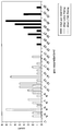
- FIG. 28 is a diagram showing variations in the nanogap length when the nanogap length is set to 5 nm or less by using an autocatalytic electroless gold plating method using iodine tincture.
- the horizontal axis in FIG. 28 is the gap length (Gap Separation) nm, and the vertical axis is the number.
- the standard deviation of the nanogap length obtained by this method is 1.7 nm.
- the inventors of the present invention have completed the present invention by controlling the gap length with higher accuracy than before by controlling the gap length by the molecular length of the surfactant molecule.
- the present inventors paid attention to a plating technique using a surfactant molecule when synthesizing nanoparticles as a protective group.
- alkyltrimethylammonium bromide Alkyltrimethylammonium Bromide
- This surfactant molecule has a straight alkyl chain, and a trimethylammonium group N (CH 3 ) 3 in which all hydrogens of the ammonium group are substituted with methyl groups is attached to the alkyl chain.
- a method for producing an electrode structure having a nanogap length is a method in which a substrate having a gap and a metal layer arranged in pairs is used as an electrolytic solution containing metal ions.
- an electroless plating solution in which a reducing agent and a surfactant are mixed, the metal ions are reduced by the reducing agent, and the metal is deposited on the metal layer while the surfactant adheres to the surface of the metal.
- an electrode pair in which the length of the gap is controlled to a nanometer size is formed.
- the method of manufacturing an electrode structure having a nanogap length includes a first step of arranging a metal layer on a substrate in a pair with a gap, and a substrate on which the metal layer is arranged in a pair with a gap.
- a metal layer By immersing in an electroless plating solution in which a reducing agent and a surfactant are mixed in an electrolytic solution containing ions, the metal ions are reduced by the reducing agent, and the surfactant is added to the metal layer while the metal is precipitated.
- the present invention has a plurality of electrode pairs arranged with nano gaps arranged side by side, and a standard deviation of each gap length of the plurality of electrode pairs is 0.5 nm. It is an electrode structure having a nanogap length of 0.6 to 0.6 nm, or a nanodevice provided with this electrode structure.
- the gap length is controlled by the molecular length by an electroless plating method using a surfactant molecule as a molecular ruler on the electrode surface.
- a gap electrode can be produced.
- an initial nanogap electrode produced by a top-down method is plated using an electroless plating method using iodine tincture, and a molecular ruler electroless plating is performed after the distance is reduced to some extent.
- the gap length can be controlled more precisely and with a high yield.
- the electrode structure having a nanogap length obtained by the production method of the present invention has a standard deviation of each gap length of 0.5 nm to 0.6 nm by changing the molecular length of the surfactant molecule.
- a plurality of electrode pairs with small variations by controlling the gap length can be provided.
- a nanodevice having a nanogap electrode such as a diode, a tunnel element, a thermoelectronic element, or a thermophotovoltaic element, can be manufactured with a high yield.
- or FIG. 1 It is sectional drawing which shows typically the preparation methods of the electrode structure which concerns on 1st Embodiment of this invention. It is a top view which shows typically the preparation method shown in FIG. It is a figure which shows typically the structure of the electrode which has the nano gap length obtained with the preparation method of the electrode structure shown in FIG. It is a figure which shows typically the chemical structure of surfactant molecule
- or (d) are the SEM images of the nano gap electrode produced by immersing the board
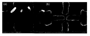
- (A), (b) is a SEM image which shows the example of the nano gap electrode produced in Example 1.
- FIG. (A), (b) is a SEM image which shows the example of the nano gap electrode produced in Example 2.
- FIG. (A), (b) is the SEM image which shows the example of the nano gap electrode produced in Example 3.
- FIG. (A), (b) is the SEM image which shows the example of the nano gap electrode produced in Example 4.
- FIG. It is a figure which shows the distribution which shows the variation in the gap in several pairs of the electrodes which have the gap length produced in Example 1.
- FIG. is a figure which shows the distribution which shows the dispersion
- FIG. It is a figure which shows the distribution which shows the variation in the gap in the several pairs of electrode which has the gap length produced in Example 3.
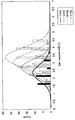
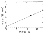
- FIG. 18 is a diagram in which the histograms shown in FIGS. 14 to 17 are superimposed. It is a figure which shows the graph which plotted the length for surfactant molecule 2 chain length, and the average value actually obtained. It is a figure which shows the relationship between carbon number n and gap length in surfactant.
- or (c) are the SEM images of the electrode which has the nano gap length produced as Example 5.
- FIG. 10 is a diagram showing a histogram of nanogap electrodes at each stage produced in Example 5.
- FIG. 10 is a diagram showing current-voltage characteristics at a liquid nitrogen temperature when the gate voltage is used as a parameter in the single-electron device manufactured in Example 6.
- Example 7 it is a SEM image of the nano gap electrode produced by immersing the board
- FIG. 10 is a diagram showing a histogram of gap length in the sample produced in Example 7. It is a figure which shows the dispersion
- Substrate 1A Semiconductor substrate 1B: Insulating film 2A, 2B, 2C, 2D: Metal layer (initial electrode) 3A, 3B, 3C, 3D: Metal layer (electrode formed by plating) 4A, 4B: Electrode 5: Surfactant (molecular ruler) 5A, 5B: Self-composing monomolecular film 6: Alkanedithiol 7: SAM mixed film 8: Nanoparticle 8A: Gold nanoparticle protected with alkanethiol 10: Nanogap electrode 11: Semiconductor substrate 12: Insulating film 13: Substrate 14A , 14B: Metal layer 15: Insulating film 16: Metal film 17: Gate insulating film 18B: Metal layer 20: Gate electrode 21: Source electrode 22: Drain electrode
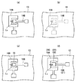
- FIG. 1 is a cross-sectional view schematically showing a method for producing an electrode structure according to the first embodiment of the present invention
- FIG. 2 is a plan view schematically showing the production method shown in FIG.
- a pair of metal layers 2A and 2B having a gap L1 is formed at an interval with respect to a substrate 1 in which an insulating film 1B is provided on a semiconductor substrate 1A. To do.
- the substrate 1 is immersed in an electroless plating solution.
- This electroless plating solution is prepared by mixing a reducing agent and a surfactant into an electrolytic solution containing metal ions.
- the metal ions are reduced by the reducing agent and the metal is deposited on the surfaces of the metal layers 2A and 2B.
- the gap between the metal layer 3A and the metal layer 3B is reduced to a distance L2, and the surfactant contained in the electroless plating solution is chemically adsorbed on the metal layers 3A and 3B formed by the precipitation. Therefore, the surfactant controls the gap length (simply called “gap length”) to the nanometer size.
- the metal ions in the electrolytic solution are reduced by the reducing agent and the metal is deposited, such a method is classified as an electroless plating method.
- the metal layers 3A and 3B are formed on the metal layers 2A and 2B by plating, and a pair of electrodes 4A and 4B is obtained.
- the electroless plating method (hereinafter referred to as “molecular ruler electroless plating method”) using surfactant molecules as protective groups on the surfaces of the electrodes 4A and 4B, the gap length is determined as the molecular length.
- a pair of electrodes (hereinafter referred to as “nano-gap electrodes”) 10 having a nano-gap length controlled in such a manner is produced.
- metal layers 2C and 2D are formed on both sides of the metal layers 2A and 2B together with the metal layers 2A and 2B, and as shown in FIG.
- metal layers 3C and 3D together with metal layers 3A and 3B on 2D by plating each metal layer 2C and metal layer 3C, and each metal layer 2D and metal layer 3D may be used as each side gate electrode.
- FIG. 3 is a diagram schematically showing the structure of an electrode having a nanogap length obtained by the method for producing the electrode structure shown in FIG.
- the nanogap electrode 10 will be described in detail while describing a method for producing the nanogap electrode 10 according to the embodiment of the present invention.
- a silicon oxide film 1B as an insulating film is formed on a Si substrate as a semiconductor substrate 1A, and initial nanogap electrodes as metal layers 2A and 2B are formed on the substrate 1 (first step).
- the metal layers 2A and 2B are formed by laminating an adhesion layer formed of Ti, Cr, Ni or the like on the substrate 1 and a layer formed of another metal such as Au, Ag, or Cu on these adhesion layers. May be.
- the metal layer is controlled by a molecular ruler with the surfactant molecule 5 (second step).
- the growth of the metal layers 3A and 3B is controlled, and as a result, the gap between the electrode 4A and the electrode 4B is precisely controlled to a nano size, and a nano gap electrode is manufactured.
- the initial nanogap electrodes as the metal layers 2A and 2B are produced by, for example, an electron beam lithography technique (hereinafter simply referred to as “EB lithography technique”).
- EB lithography technique an electron beam lithography technique
- the gap length at that time depends on the performance and yield of the electron beam lithography technique, but is, for example, in the range of 20 nm to 100 nm.
- the gate electrode can be grown simultaneously by electroless plating, and the gate electrode can be made closer to a single electron island.
- the plating solution which is a mixed solution, contains a surfactant that functions as a molecular ruler, and an aqueous solution in which deposited metal cations are mixed, for example, an aqueous solution of gold chloride (III) acid and a reducing agent.
- This mixed solution preferably contains an acid as described later.
- an alkyltrimethylammonium bromide (Alkyltrimethylammonium bromide) molecule is used.
- alkyltrimethylammonium bromide include decyltrimethylammonium bromide (DTAB), lauryltrimethylammonium bromide (LTAB), myristyltrimethylammonium bromide (MTAB), and odor.
- DTAB decyltrimethylammonium bromide
- LTAB lauryltrimethylammonium bromide
- MTAB myristyltrimethylammonium bromide
- CTAB Cetyltrimethylammonium bromide
- molecular rulers include alkyl trimethyl ammonium halide, alkyl trimethyl ammonium chloride, alkyl trimethyl ammonium iodide, dialkyl dimethyl ammonium bromide, dialkyl dimethyl ammonium chloride, dialkyl dimethyl ammonium iodide, alkyl benzyl dimethyl ammonium bromide.
- examples of the long-chain aliphatic alkyl group include alkane groups such as hexyl, octyl, decyl, dodecyl, tetradecyl, hexadecyl, and octadecyl, and alkylene groups. Since it is expected, it is not limited to these examples.
- an organic solvent is a gold chloride (III) acid aqueous solution, a sodium chloride gold (III) acid aqueous solution, a potassium chloride gold (III) acid aqueous solution, a gold chloride (III) aqueous solution, or an ammonium chloride gold (III) acid salt.
- the ammonium salt include the ammonium salts described above
- examples of the organic solvent include aliphatic hydrocarbons, benzene, toluene, chloromethane, dichloromethane, chloroform, and carbon tetrachloride.
- ascorbic acid Ascorbic acid, hydrazine, primary amine, secondary amine, primary alcohol, secondary alcohol, polyol containing diol, sodium sulfite, hydroxylammonium borohydride, lithium aluminum hydride, oxalic acid, formic acid, etc. Is mentioned.
- Ascorbic acid which has a relatively low reducing power, for example, enables reduction of gold to zero valence by autocatalytic plating using the electrode surface as a catalyst. If the reducing power is strong, reduction occurs outside the electrode and many clusters are generated. That is, it is not preferable because gold fine particles are generated in the solution and gold cannot be selectively deposited on the electrode. Conversely, if it is a weaker reducing agent such as ascorbic acid, the autocatalytic plating reaction will not proceed.
- a cluster is a gold nanoparticle formed by plating on a nucleus that enables electroless plating on the surface.
- L (+)-ascorbic acid is used as a reducing agent because it has a weak reducing action among the reducing agents described above, reduces the formation of clusters, and reduces gold to zero using the electrode surface as a catalyst. Is preferred.
- the electroless plating solution is preferably mixed with an acid that functions to suppress the formation of clusters. This is because the cluster can be dissolved in an unstable state where it has begun to nucleate.
- an acid hydrochloric acid, nitric acid, and acetic acid can be used.
- FIG. 4 is a diagram schematically showing the chemical structure of a surfactant molecule (CTAB) used as a molecular ruler.
- CTAB is a molecule having an alkyl chain length of C16, that is, 16 straight-chain carbon atoms.
- four molecules are shown as an example of the best mode, including derivatives having different alkyl chains, DTAB as the alkyl chain C10, LTAB as the C12, and MTAB as the C14.
- the acronyms L, M, and C are taken from the acronyms Lauryl meaning 12, 12 Myristyl, and 16 Cetyl, respectively.
- the plating in the embodiment of the present invention is an autocatalytic electroless gold plating, it is deposited on the surface of the gold electrode serving as a nucleus. This makes it possible to reduce gold to zero using the gold electrode as a catalyst since the reducing power of ascorbic acid is weak.
- the pH and temperature of the plating solution are approximately in the range of 25 ° C. to 90 ° C., although depending on the type of surfactant, particularly the number of linear carbons.
- the pH range is around 2-3. If it is out of this range, it is difficult to perform gold plating, which is not preferable.
- the pair of metal layers 2A and 2B is formed on the substrate 1 with the insulating film 1B.
- a pair of metal layers having a certain gap is formed on the substrate 1 by using a lithography technique. This “degree” is appropriately determined according to the accuracy of the electron beam lithography technique.
- Dissolve gold as [AuI 4 ] ⁇ ions by dissolving the gold foil in the iodine tincture solution.
- the reducing agent L (+)-ascorbic acid is added thereto to perform autocatalytic electroless gold plating on the gold electrode surface.
- a pair of metal layers 2A and 2B is formed by an iodine electroless plating method.
- the pair of metal layers 2A and 2B can be arranged close to each other on one surface side of the substrate 1, that is, the gap length of the initial electrode as the metal layers 2A and 2B is shortened. be able to.
- the metal layer 2 ⁇ / b> A and the metal layer 2 ⁇ / b> B can be formed with high accuracy with a gap in the range of several nm to about 10 nm.
- the substrate 1 is immersed in an electroless plating solution.
- the time for immersing the substrate 1 in the electroless plating solution that is, the plating time can be shortened. Yield reduction due to the formation of clusters can be suppressed.
- the time for immersing the substrate 1 in the mixed solution in the second step becomes long.
- the plating time becomes long and clusters are formed.
- the yield is lowered by the gold clusters adhering to the outer peripheral surface of the portion to be the electrode. According to the second embodiment of the present invention, it is possible to suppress a decrease in yield.
- Electrode structure with nanogap length and device using it Next, an electrode structure having a nanogap length obtained by the method for producing an electrode structure having a nanogap length according to the first and second embodiments of the present invention will be described.
- An electrode structure having a nanogap length has a plurality of electrode pairs arranged with a nanogap arranged side by side, and a standard deviation of each gap length of the plurality of electrode pairs is within a predetermined range. It is within.
- the predetermined range is a standard deviation of 0.5 nm to 0.6 nm as in Example 1 described later. Thus, the gap length variation is small.
- the electrode pair is a source electrode and a drain electrode
- various devices such as a single electron device can be efficiently obtained by providing a side gate electrode on the side of the source electrode and the drain electrode.
- a thermal oxide film of the insulating film 1B of the substrate 1 is used as the channel.
- a single electronic device using the nanogap electrode 10 manufactured by a molecular ruler electroless plating method will be described as a single electronic device.
- a single electronic device using gold nanoparticles having an organic molecule as a protecting group will be described, and the evaluation of the effectiveness of a gold nanogap electrode produced by an electroless gold plating method will also be described.
- As a production step a method for fixing particles between electrodes will be described first.
- a single-electron device using gold nanoparticles having an organic molecule as a protecting group is obtained by using ligand exchange of alkanethiol-protected gold nanoparticles with dithiol molecules between gold nanogap electrodes prepared as described above. Nanoparticles are chemically bonded, for example, fixed to a self-composing monomolecular film. Coulomb blockade characteristics are observed at liquid nitrogen temperature.
- FIG. 5 schematically shows a process for installing a single electron island by chemical bonding using dithiol molecules on the electrodes 4A and 4B in the electrode structure having a nanogap length produced as shown in FIGS.
- FIG. 5A self-assembled monolayers (SAMs) 5A and 5B are formed on the gold electrode surfaces as the electrodes 4A and 4B.
- SAMs self-assembled monolayers
- FIG. 5B by introducing the alkanedithiol 6, the alkanedithiol is coordinated to the SAM deficient portion, and the SAM mixed film 7 composed of SAM and alkanethiol is formed.
- alkanethiol-protected gold nanoparticles 8A are introduced.
- a gold nanogap electrode was used by introducing nanoparticles 8 as single-electron islands by chemical adsorption using self-assembled monolayers 6A and 6B between electrodes having nanogap lengths.
- the device can be configured.
- the electrode structure having a nanogap shown in FIGS. 1 to 5 is a structure in which electrodes are arranged horizontally, but the embodiment of the present invention may be a vertical stacked electrode structure.
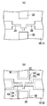
- FIG. 6 is a plan view showing a device manufacturing process of an electrode structure having a nanogap according to a third embodiment of the present invention.
- FIG. 7 is a cross-sectional view showing a manufacturing process of a device having an electrode structure provided with a nanogap according to a third embodiment of the present invention.
- a substrate 13 in which an insulating film 12 such as SiO 2 is provided on a semiconductor substrate 11 such as Si is prepared, a resist film is formed, and then electron beam lithography or optical lithography is performed so as to form a gate electrode and a drain electrode.
- the pattern is formed by exposing to light.
- metal layers 14A and 14B that are part of the gate electrode and the source electrode are formed (see FIGS. 6A and 7A). At that time, the distance between the metal layer 14A and the metal layer 14B is L 11.
- a drain electrode is deposited to form a metal film 16 (FIG. 6B, (Refer FIG.7 (b)).
- PECVD plasma enhancement CVD
- exposure is performed using electron beam lithography or optical lithography to form a pattern so as to form the drain electrode.
- etching is performed by RIE (Reactive Ion Etching) or CDE (Chemical ⁇ Dry Etching) until the metal layer 18B as a part of the drain electrode and the gate insulating film 17 are formed.
- etching is performed in the vertical direction with respect to the substrate 13 so that the drain electrode and the insulating film have the shape of the drain electrode, and etching is performed until the surface of the formed source electrode comes out.
- the size of the drain electrode is made smaller than the shape of the formed source electrode in consideration of the size of misalignment + ⁇ .
- the gap between the source electrode and the drain electrode is reduced by combining only the molecular ruler electroless plating method or the iodine electroless plating method. Since the gate insulating film 17 has a thickness of about 10 nm, only the molecular ruler electroless plating process may be performed.
- plating grows in the direction in which the edge of the metal layer 18B as a part of the drain electrode extends horizontally, and the metal layer 14B as a part of the source electrode grows upward, The metal layer 14A grows inward as a part of the gate electrode (see FIGS. 6D and 7D).
- the grown film portions at this time are denoted by reference numerals 19A, 19B, and 19C, respectively.
- the gate electrode 20, source electrode 21, the distance between electrodes of the drain electrode 22 is narrow, for example, FIG. 6 (a), the spacing was the distance L 11 in FIGS. 7 (a) becomes L 12. Therefore, the gate capacitance increases.
- nanoparticles are introduced in the manner described with reference to FIG.
- a passivation film is formed, and the source electrode, drain electrode, and gate electrode die are opened to complete the process. Thereby, a single electron transistor can be formed.
- the shape of the electrode forming the nanogap electrode by molecular ruler plating may be a vertical and stacked electrode shape.
- the thickness of the insulator existing between the source / drain electrodes can be increased, and the leakage current can be reduced.
- the gap length of the nano gap existing around the electrode is preferable because it can be controlled by a molecular ruler.
- the electrode material may be copper as the initial electrode material.
- a copper electrode is formed by using an electron beam lithography method or a photolithographic method, and then the surface of the copper electrode is made copper chloride.
- a gold chloride solution using ascorbic acid as a reducing agent is used as a plating solution, and the copper electrode surface is covered with gold. This technique is disclosed in Non-Patent Document 16, for example.
- a surfactant alkyltrimethylammonium bromide C n H 2n + 1 [CH 3 ] 3 N + ⁇ Br ⁇ is mixed with an aqueous solution of gold chloride (III), and the reducing agent L (+)-ascorbic acid is added.
- autocatalytic electroless gold plating is performed on the gap electrode.
- a nanogap electrode having a gold surface is prepared by molecular ruler plating.
- the nanogap length is accurately and precisely controlled by the method for producing an electrode structure having a nanogap length according to an embodiment of the present invention, and will be specifically described with reference to examples.
- a nanogap electrode was produced using the molecular ruler electroless plating method described in the first embodiment in the following manner.
- a silicon substrate having a silicon oxide film as an insulating film 1B is prepared on a silicon substrate as a substrate 1A, a resist is applied on the substrate 1, and a metal having a gap length of 30 nm is formed by EB lithography technology.
- the pattern of the initial electrode as the layers 2A and 2B was drawn.
- a 2 nm Ti film was deposited by EB deposition, and Au was deposited on the Ti film by 10 nm to prepare initial gold nanogap electrodes as metal layers 2A and 2B.
- a plurality of pairs of metal layers 2A and 2B were provided on the same substrate 1.
- an electroless plating solution was prepared.
- As a molecular ruler measure 25 milliliters of 25 mM alkyltribromide BR> ⁇ ruammonium (ALKYLTRIMETHYLAMMONIUMMBROMIDE). There, 120 microliters of 50 mmol of chloroauric acid aqueous solution is measured. 1 ml of acetic acid was added as an acid, and 0.1 mol and 3.6 ml of L (+)-ascorbic acid (ASCORBIC ACID) serving as a reducing agent was added and stirred well to obtain a plating solution.
- ASCORBIC ACID L (+)-ascorbic acid
- Example 1 DTAB molecules were used as alkyltrimethylammonium bromide.
- An already prepared substrate with a gold nanogap electrode was immersed in an electroless plating solution for about 30 times.
- an electrode having a nanogap length was produced by the molecular ruler electroless plating method of Example 1.
- FIG. 8 shows the fabrication of a plurality of pairs of electrodes 2A and 2B as initial nanogap electrodes on a silicon (Si) substrate 1A provided with a silicon oxide film (SiO 2 ) as an insulating film 1B by using EB lithography technology. It is a part of SEM image which observed this. From the SEM image, the gap length of the initial electrode as the metal layers 2A and 2B was 30 nm.
- the length of the electrode having a nanogap length produced as Example 1 was measured by observing an image by SEM.
- the size of one pixel in the SEM image acquired at a high magnification of 200,000 times is in steps of 0.5 nm from the resolution.
- the length was measured by enlarging to the point where the evaluation of 1 pixel size was possible, and increasing the contrast ratio so that the difference between the gap area and the substrate 1 became clear from the gap height and SEM characteristics. .
- FIG. 9 is an SEM image of the nanogap electrode produced by immersing the substrate with the initial nanogap electrode shown in FIG. 8 in a molecular ruler plating solution.
- (A), (b), (c), and (d) of FIG. 9 are images obtained by extracting a part of a plurality of pairs on one substrate.
- FIG. 9A is an electrode with a gap length of 5 nm or more
- FIG. 9B is an electrode with a gap length of 5 nm or less but which is considered not to suppress growth
- FIG. 9D is a gap based on a molecular ruler.
- the metal layer 3A and the metal layer 3B, that is, the state in which the source electrode and the drain electrode are connected are shown.
- the average value and the dispersion value were calculated for each molecular ruler thus measured. Moreover, normal distribution was calculated using them. With the measured data histogram and normal distribution, it is possible to confirm the precise control of the gap length of the nanogap electrode depending on the molecular length of the molecular ruler.
- FIG. 10 is an SEM image showing an example of the nanogap electrode produced in Example 1.
- the gap length was 1.49 nm
- the gap length was 2.53 nm.
- Example 2 an electrode having a nanogap length was produced by a molecular ruler electroless plating method in the same manner as in Example 1 except that LTAB molecules were used as alkyltrimethylammonium bromide.
- FIG. 11 is an SEM image showing an example of the nanogap electrode produced in Example 2. In FIG. 11A, the gap length was 1.98 nm, and in FIG. 11B, the gap length was 2.98 nm.
- Example 3 an electrode having a nanogap length was produced by a molecular ruler electroless plating method in the same manner as in Example 1 except that MTAB molecules were used as alkyltrimethylammonium bromide.
- FIG. 12 is an SEM image showing an example of a nanogap electrode produced in Example 3. In FIG. 12A, the gap length was 3.02 nm, and in FIG. 12B, the gap length was 2.48 nm.
- Example 4 an electrode having a nanogap length was produced by a molecular ruler electroless plating method in the same manner as in Example 1 except that CTAB molecules were used as alkyltrimethylammonium bromide.
- FIG. 13 is an SEM image showing an example of a nanogap electrode produced in Example 4. In FIG. 13A, the gap length was 3.47 nm, and in FIG. 13B, the gap length was 2.48 nm.
- Example 1 The average and standard deviation of the gap lengths in the electrodes having the nanogap length produced in Examples 1 to 4 were calculated.
- Example 1 DTAB molecules were used as the surfactant, and the gap length of the 25 gap length electrodes was 2.31 nm on average and 0.54 nm in standard deviation.
- Example 2 LTAB molecules were used as the surfactant, and the average gap length in the electrode having 44 gap lengths was 2.64 nm and the standard deviation was 0.52 nm.
- Example 3 MTAB molecules were used as the surfactant, and the average gap length in an electrode having 50 gap lengths was 3.01 nm and the standard deviation was 0.58 nm.
- Example 4 CTAB molecules were used as the surfactant, and the average gap length in the electrode having 54 gap lengths was 3.32 nm and the standard deviation was 0.65 nm.
- FIG. 14 is a distribution diagram showing gap variation in a plurality of pairs of electrodes having gap lengths produced in Example 1.
- FIG. 15 is a distribution diagram showing gap variation in a plurality of pairs of electrodes having a gap length produced in Example 2.
- FIG. 16 is a distribution diagram showing gap variation in a plurality of pairs of electrodes having gap lengths produced in Example 3.
- FIG. 17 is a distribution diagram showing gap variation in a plurality of pairs of electrodes having gap lengths produced in Example 4.
- FIG. 18 is a diagram in which the histograms shown in FIGS. 14 to 17 are superimposed. Any distribution can be approximated to a normal distribution.
- FIG. 19 is a graph showing a plot of the length of the surfactant molecule and the average value actually obtained.
- FIG. 20 is a graph showing the relationship between the number of carbons n and the gap length in the surfactant. From this figure, it can be seen that the carbon number n and the gap length are in a linear relationship. Thus, it can be seen that the average value of the gap length is linear with respect to the carbon number of the surfactant. From these, it can be seen that the nanogap electrode produced by the molecular ruler electroless plating method is controlled depending on the chain length of the molecular ruler.
- the growth of the nanogap electrode is achieved by meshing with one or two alkyl chain lengths as shown in the schematic diagram of FIG. It can be seen that is controlled.
- the electroless plating method using iodine makes it possible to produce a nanogap electrode with a yield of 90% (Yield) of 5 nm or less.
- the standard deviation at that time was 1.37 nm.
- Example 1 to Example 4 in the electroless plating method using a molecular ruler, the surfactant is adsorbed on the growth surface, so that the gap between the nanogaps is filled with the surfactant.
- the gap length based on the molecular length could be controlled.
- the standard deviation of the gap length is suppressed to 0.52 nm to 0.65 nm, and it can be seen that the gap length can be controlled with very high accuracy.
- the yield was about 10%. This is because the growth is very slow compared to plating using iodine tincture, so that clusters are likely to be generated, and the probability that the clusters adhere to the electrode portion and short-circuit increases.
- foil-like gold was dissolved in the iodine tincture solution as [AuI 4 ] ⁇ ions.
- L (+)-ascorbic acid was added to perform autocatalytic plating on the gold electrode surface.
- the initial nanogap electrode fabricated by top-down using the autocatalytic iodine electroless plating method was plated, and after shortening the distance to some extent, molecular ruler plating was performed for a shorter time. Then, generation
- FIG. 21 is an SEM image of an electrode having a nanogap length produced as Example 5.
- 21A is an initial electrode (23.9 nm)
- FIG. 21B is a nanogap electrode after iodine plating (9.97 nm)
- FIG. 21C is a nanogap plated using DTAB as a molecular ruler. It is each SEM image of an electrode (1.49 nm).
- FIG. 22 is a diagram showing a histogram of the nanogap electrode at each stage produced in Example 5.
- the self-stop is caused by the molecular ruler length. That is, the gap was controlled at equal intervals with a width of 5 nm or more, and the yield of the nanogap electrode was dramatically increased from 10% to 37.9%. In this way, it was confirmed that the yield was improved by performing molecular ruler electroless plating on the nanogap electrode after iodine electroless plating.
- a single-electron device in which gold nanoparticles were fixed between gold nanogap electrodes was fabricated.
- the molecules adhering to the surface were incinerated by performing O 2 plasma ashing on the nanogap electrode produced by the molecular ruler electroless plating method.
- the sample was immersed for 12 hours in a solution of octanethiol (C8S) mixed in an ethanol solution to 1 mmol, and rinsed twice with ethanol.
- C10S2 decanedithiol
- FIG. 23 is a diagram schematically showing the state of particle introduction of the single-electron device produced in Example 6.
- the single-electron device is provided with first and second gate electrodes (Gate1, Gate2) on both sides where the drain electrode (D) and the source electrode (S) face each other.
- C10-protected gold nanoparticles 8 are disposed between the nanogap between the drain electrode and the source electrode.
- tunnel junctions by SAM Self-Assembled-Monolayer
- SAM Self-Assembled-Monolayer
- R1 and R2 are generally considered to be due to SAM, that is, alkanethiol / alkanedithiol.
- Non-Patent Documents 17 and 18 have reported that the resistance value of SAM changes by about one digit when the number of carbons changes by two (Non-Patent Documents 17 and 18). Therefore, it is possible to calculate which molecule is joined by the values of R1 and R2 obtained from the theoretical fitting.
- FIG. 24 shows the current-voltage characteristics of the electrode 1 and the electrode 2 that are not modulated by the gate electrode, (a) shows the overall current-voltage characteristics, and (b) is an enlarged view thereof.
- Vd potential difference
- R1 and R2 values are estimated to be 6.0 G ⁇ and 5.9 G ⁇ by fitting with theoretical values, and it is considered that both values are octanethiols. This indicates that the introduction of particles by chemisorption is not successful.
- FIG. 25 is a diagram illustrating current-voltage characteristics of the electrode 1 and the electrode 2 that are not modulated by the gate electrode. From the figure, it was possible to observe the gate modulation effect of changing the width of the Coulomb blockade by changing the ease of entry of electrons into the gold single-electron island when gate modulation was applied. Utilizing such a modulation effect is considered to be the operation of a single-electron device and has been found to have utility as an electrode. As shown in FIG. 25, gate modulation using a gate electrode is possible, and the usefulness of this electrode as a single-electron device can be recognized.
- Example 7 decamethonium bromide was used as the surfactant. Similar to Example 1, an initial gold nanogap electrode was produced.
- an electroless plating solution was prepared.
- As a molecular ruler measure 28 milliliters of 25 millimoles of decamethonium bromide. There, 120 milliliters of 50 millimoles of a gold chloride (III) acid aqueous solution is measured. 1 ml of acetic acid was added as an acid, 0.1 mol of L (+)-ascorbic acid (Ascorbic acid) as a reducing agent and 3.6 ml of acid were added and stirred well to obtain a plating solution.
- An already prepared substrate with a gold nanogap electrode was immersed in an electroless plating solution for about 30 minutes.
- an electrode having a nanogap length was produced by the molecular ruler electroless plating method of Example 7.
- FIG. 26 is an SEM image of a nanogap electrode produced by immersing a substrate with an initial nanogap electrode in a molecular ruler plating solution. When the gap length reached 1.6 nm, it was found that the growth of the plating was self-stopping.
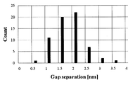
- FIG. 27 is a diagram showing a histogram of the gap length in the sample produced in Example 7.
- the horizontal axis is the gap length nm, and the vertical axis is the count.
- the average value of the gap length was 2.0 nm. This value was smaller than those of Examples 1 to 4.
- the number of samples was 64, and the standard deviation was 0.56 nm, the minimum value was 1.0 nm, the median value was 2.0 nm, and the maximum value was 3.7 nm.
- the molecular length of decamethonium bromide, which is the surfactant in Example 7, is 1.61 nm
- the molecular length of CTAB, which is the surfactant in Example 4 is 1.85 nm. This is consistent with the fact that the molecular length is short and the gap between nanogap is narrow. From these results, it was found that the nanogap length can be controlled by the molecular length of the surfactant.
- the nanogap electrode whose gap length is precisely controlled by the molecular ruler electroless plating method of the present invention has a very narrow gap between the electrodes, a diode, a tunnel element, a thermoelectronic element can be obtained by using this nanogap electrode. It plays an important role in the manufacture of nanodevices that require nanogap electrodes, such as thermophotovoltaic elements.
Landscapes
- Chemical & Material Sciences (AREA)
- Engineering & Computer Science (AREA)
- Nanotechnology (AREA)
- Crystallography & Structural Chemistry (AREA)
- Materials Engineering (AREA)
- Mechanical Engineering (AREA)
- Metallurgy (AREA)
- Organic Chemistry (AREA)
- General Chemical & Material Sciences (AREA)
- Chemical Kinetics & Catalysis (AREA)
- Physics & Mathematics (AREA)
- Manufacturing & Machinery (AREA)
- General Physics & Mathematics (AREA)
- Condensed Matter Physics & Semiconductors (AREA)
- Mathematical Physics (AREA)
- Theoretical Computer Science (AREA)
- Chemically Coating (AREA)
- Electrodes Of Semiconductors (AREA)
- Thin Film Transistor (AREA)
Abstract
Priority Applications (5)
| Application Number | Priority Date | Filing Date | Title |
|---|---|---|---|
| JP2013503464A JP5942297B2 (ja) | 2011-03-08 | 2012-02-28 | ナノギャップ長を有する電極構造の作製方法、メッキ液及びナノデバイス |
| CN201280012185.7A CN103563052B (zh) | 2011-03-08 | 2012-02-28 | 具有纳米间隙长度的电极结构的制作方法、通过该方法得到的具有纳米间隙长度的电极结构和纳米器件 |
| KR1020137026296A KR101572228B1 (ko) | 2011-03-08 | 2012-02-28 | 나노 갭 길이를 가지는 전극 구조의 제작 방법 및 그것에 의해 얻어지는 나노 갭 길이를 가지는 전극 구조, 및 나노 디바이스 |
| US14/003,679 US20140054788A1 (en) | 2011-03-08 | 2012-02-28 | Method for fabricating nanogap electrodes, nanogap electrodes array, and nanodevice with the same |
| US15/069,879 US20160300915A1 (en) | 2011-03-08 | 2016-03-14 | Method for fabricating nanogap electrodes, nanogap electrodes array, and nanodevice with the same |
Applications Claiming Priority (2)
| Application Number | Priority Date | Filing Date | Title |
|---|---|---|---|
| JP2011050894 | 2011-03-08 | ||
| JP2011-050894 | 2011-03-08 |
Related Child Applications (2)
| Application Number | Title | Priority Date | Filing Date |
|---|---|---|---|
| US14/003,679 A-371-Of-International US20140054788A1 (en) | 2011-03-08 | 2012-02-28 | Method for fabricating nanogap electrodes, nanogap electrodes array, and nanodevice with the same |
| US15/069,879 Division US20160300915A1 (en) | 2011-03-08 | 2016-03-14 | Method for fabricating nanogap electrodes, nanogap electrodes array, and nanodevice with the same |
Publications (2)
| Publication Number | Publication Date |
|---|---|
| WO2012121067A1 true WO2012121067A1 (fr) | 2012-09-13 |
| WO2012121067A8 WO2012121067A8 (fr) | 2013-01-03 |
Family
ID=46798035
Family Applications (1)
| Application Number | Title | Priority Date | Filing Date |
|---|---|---|---|
| PCT/JP2012/055002 Ceased WO2012121067A1 (fr) | 2011-03-08 | 2012-02-28 | Procédé de fabrication de structure d'électrode ayant une longueur d'espace nanoscopique, structure d'électrode ayant une longueur d'espace nanoscopique ainsi obtenue, et nanodispositif |
Country Status (5)
| Country | Link |
|---|---|
| US (2) | US20140054788A1 (fr) |
| JP (1) | JP5942297B2 (fr) |
| KR (1) | KR101572228B1 (fr) |
| CN (2) | CN103563052B (fr) |
| WO (1) | WO2012121067A1 (fr) |
Cited By (5)
| Publication number | Priority date | Publication date | Assignee | Title |
|---|---|---|---|---|
| WO2014142040A1 (fr) * | 2013-03-09 | 2014-09-18 | 独立行政法人科学技術振興機構 | Élément électronique |
| WO2015033600A1 (fr) | 2013-09-06 | 2015-03-12 | 独立行政法人科学技術振興機構 | Paire d'électrodes, procédé de production, substrat pour dispositif et dispositif |
| CN105144388A (zh) * | 2013-03-09 | 2015-12-09 | 国立研究开发法人科学技术振兴机构 | 逻辑计算元件 |
| US10170547B2 (en) | 2014-08-29 | 2019-01-01 | Japan Science And Technology Agency | Nanodevice |
| WO2020071025A1 (fr) * | 2018-10-02 | 2020-04-09 | 国立研究開発法人科学技術振興機構 | Structure hétéroépitaxiale et son procédé de production, produit stratifié métallique contenant une structure hétéroépitaxiale et son procédé de production, et électrode à nanoécartement et procédé de production d'électrode à nanoécartement |
Families Citing this family (27)
| Publication number | Priority date | Publication date | Assignee | Title |
|---|---|---|---|---|
| US20150174613A1 (en) * | 2013-12-19 | 2015-06-25 | Sk Innovation Co., Ltd. | Method for fabricating flexible nano structure |
| KR102192973B1 (ko) * | 2013-12-19 | 2020-12-18 | 에스케이이노베이션 주식회사 | 나노 구조체를 갖는 센서 및 그 제조 방법 |
| US9725313B2 (en) * | 2013-12-19 | 2017-08-08 | Sk Innovation Co., Ltd. | Method for fabricating NANO structure including dielectric particle supporters |
| KR20150072292A (ko) * | 2013-12-19 | 2015-06-29 | 에스케이이노베이션 주식회사 | 플렉시블 기반 나노 구조체를 갖는 센서 및 그 제조 방법 |
| US20150179738A1 (en) * | 2013-12-19 | 2015-06-25 | Sk Innovation Co., Ltd. | Flexible nano structure |
| US9324628B2 (en) | 2014-02-25 | 2016-04-26 | International Business Machines Corporation | Integrated circuit heat dissipation using nanostructures |
| CN113985017A (zh) | 2016-01-14 | 2022-01-28 | 罗斯韦尔生物技术股份有限公司 | 分子传感器及相关方法 |
| JP7280590B2 (ja) * | 2016-01-28 | 2023-05-24 | ロズウェル バイオテクノロジーズ,インコーポレイテッド | 大スケールの分子電子工学センサアレイを使用する被分析物を測定するための方法および装置 |
| EP3408219B1 (fr) | 2016-01-28 | 2022-08-17 | Roswell Biotechnologies, Inc | Appareil de séquençage d'adn massivement parallèle |
| KR20240170584A (ko) | 2016-02-09 | 2024-12-03 | 로스웰 엠이 아이엔씨. | 전자 비표지 dna 및 게놈 시퀀싱 |
| US10484590B2 (en) * | 2016-03-04 | 2019-11-19 | Taiwan Semiconductor Manufacturing Co., Ltd. | Integrated circuit device |
| CA3052140A1 (fr) | 2017-01-19 | 2018-07-26 | Roswell Biotechnologies, Inc. | Dispositifs de sequencage a semi-conducteurs comprenant des materiaux de couche bidimensionnelle |
| US10475793B2 (en) | 2017-04-24 | 2019-11-12 | Taiwan Semiconductor Manufacturing Co., Ltd. | Capacitor cell and structure thereof |
| US10508296B2 (en) | 2017-04-25 | 2019-12-17 | Roswell Biotechnologies, Inc. | Enzymatic circuits for molecular sensors |
| EP3615685B1 (fr) | 2017-04-25 | 2025-02-19 | Roswell Biotechnologies, Inc | Circuits enzymatiques pour capteurs moléculaires |
| EP4023764A3 (fr) | 2017-05-09 | 2022-09-21 | Roswell Biotechnologies, Inc. | Circuits de sonde de liaison pour capteurs moléculaires |
| CN111373049A (zh) | 2017-08-30 | 2020-07-03 | 罗斯威尔生命技术公司 | 用于dna数据存储的进行性酶分子电子传感器 |
| CN111373051A (zh) | 2017-10-10 | 2020-07-03 | 罗斯威尔生命技术公司 | 用于无扩增dna数据存储的方法、装置和系统 |
| KR101948072B1 (ko) * | 2018-01-29 | 2019-02-14 | 주식회사 페타룩스 | 전자소자 제조방법 |
| TWI772618B (zh) * | 2018-03-02 | 2022-08-01 | 國立研究開發法人科學技術振興機構 | 奈米縫隙電極及其製作方法以及具有奈米縫隙電極的奈米裝置 |
| US10590541B2 (en) * | 2018-06-15 | 2020-03-17 | Rohm And Haas Electronic Materials Llc | Electroless copper plating compositions and methods for electroless plating copper on substrates |
| JP7228411B2 (ja) * | 2019-03-06 | 2023-02-24 | 上村工業株式会社 | 無電解金めっき浴 |
| CN113994013A (zh) | 2019-04-12 | 2022-01-28 | 罗斯威尔生命技术公司 | 用于分子电子学传感器的多环芳族桥 |
| US12146852B2 (en) | 2019-09-06 | 2024-11-19 | Roswell Biotechnologies, Inc. | Methods of fabricating nanoscale structures usable in molecular sensors and other devices |
| CN111893527A (zh) * | 2020-08-04 | 2020-11-06 | 淮南师范学院 | 纳米电极对及其制备方法 |
| CN115132578B (zh) * | 2022-09-01 | 2022-12-30 | 中国科学技术大学 | 一种具有纳米间隙的电极对及其制备方法 |
| CN116013781A (zh) * | 2023-02-22 | 2023-04-25 | 北京集创北方科技股份有限公司 | 一种金属阵列的制备方法,该金属阵列以及使用该金属阵列的肖特基二极管和电容器 |
Citations (4)
| Publication number | Priority date | Publication date | Assignee | Title |
|---|---|---|---|---|
| JP2005513818A (ja) * | 2001-12-21 | 2005-05-12 | プラスティック ロジック リミテッド | 自己整合印刷 |
| JP2006209982A (ja) * | 2005-01-25 | 2006-08-10 | Seiko Epson Corp | 電子放出素子、電子放出素子の製造方法、及び電気光学装置、並びに電子機器 |
| JP2008192712A (ja) * | 2007-02-01 | 2008-08-21 | Japan Science & Technology Agency | トンネル磁気抵抗素子 |
| JP2009535837A (ja) * | 2006-05-02 | 2009-10-01 | コリア リサーチ インスティテュート オブ スタンダーズ アンド サイエンス | ナノギャップ電極の製造方法及びこれを用いて製造されたナノギャップ素子 |
Family Cites Families (23)
| Publication number | Priority date | Publication date | Assignee | Title |
|---|---|---|---|---|
| US3684572A (en) * | 1970-07-13 | 1972-08-15 | Du Pont | Electroless nickel plating process for nonconductors |
| CN87100440B (zh) * | 1987-01-27 | 1988-05-11 | 中国人民解放军装甲兵工程学院 | 在不导电材料上刷镀铜的方法 |
| JP2819180B2 (ja) * | 1990-02-22 | 1998-10-30 | 信康 土肥 | すず―鉛―ビスマス合金めっき浴 |
| US5282953A (en) * | 1993-06-28 | 1994-02-01 | Technic Incorporated | Polyoxyalklene compounds terminated with ketone groups for use as surfactants in alkanesulfonic acid based solder plating baths |
| EP0865078A1 (fr) * | 1997-03-13 | 1998-09-16 | Hitachi Europe Limited | Méthode de dépÔt de particules nanométriques |
| JP4932094B2 (ja) * | 2001-07-02 | 2012-05-16 | 日本リーロナール有限会社 | 無電解金めっき液および無電解金めっき方法 |
| US7052616B2 (en) * | 2001-08-14 | 2006-05-30 | The Penn State Research Foundation | Fabrication of molecular scale devices using fluidic assembly |
| WO2003091159A1 (fr) * | 2002-04-25 | 2003-11-06 | General Electric Company | Preparation de compose de cuivre (i) d'une taille de particule de l'ordre du nanometre |
| US7166152B2 (en) * | 2002-08-23 | 2007-01-23 | Daiwa Fine Chemicals Co., Ltd. | Pretreatment solution for providing catalyst for electroless plating, pretreatment method using the solution, and electroless plated film and/or plated object produced by use of the method |
| CN101284313B (zh) * | 2003-09-05 | 2011-05-25 | 三菱麻铁里亚尔株式会社 | 金属微粒的制造方法及含有该微粒的组合物 |
| US7306823B2 (en) * | 2004-09-18 | 2007-12-11 | Nanosolar, Inc. | Coated nanoparticles and quantum dots for solution-based fabrication of photovoltaic cells |
| US7312155B2 (en) * | 2004-04-07 | 2007-12-25 | Intel Corporation | Forming self-aligned nano-electrodes |
| WO2006137891A2 (fr) * | 2004-09-29 | 2006-12-28 | University Of Florida Research Foundation, Inc. | Detection de substances chimiques, de particules et de biocomposes faisant appel a la nanotechnologie |
| KR100679704B1 (ko) * | 2005-01-10 | 2007-02-06 | 한국과학기술원 | 분자소자와 바이오 센서를 위한 나노갭 또는 나노 전계효과 트랜지스터 제작방법 |
| US7833904B2 (en) * | 2005-06-16 | 2010-11-16 | The Trustees Of Columbia University In The City Of New York | Methods for fabricating nanoscale electrodes and uses thereof |
| US7655566B2 (en) * | 2005-07-27 | 2010-02-02 | Semiconductor Energy Laboratory Co., Ltd. | Method for manufacturing semiconductor device |
| US7419849B2 (en) * | 2006-02-06 | 2008-09-02 | Matsushita Electric Industrial Co., Ltd. | Method for producing single electron semiconductor element |
| JP4379450B2 (ja) * | 2006-08-22 | 2009-12-09 | ソニー株式会社 | 電子デバイス及びその製造方法 |
| JP5141943B2 (ja) * | 2006-12-13 | 2013-02-13 | 独立行政法人科学技術振興機構 | 分子素子 |
| US8298620B2 (en) * | 2008-05-13 | 2012-10-30 | North Carolina Agricultural And Technical State University | Methods of preparing thin films by electroless plating |
| JP5622360B2 (ja) * | 2009-01-16 | 2014-11-12 | ローム・アンド・ハース・エレクトロニック・マテリアルズ,エル.エル.シー. | 電気錫めっき液および電気錫めっき方法 |
| JP5455415B2 (ja) * | 2009-04-10 | 2014-03-26 | 株式会社船井電機新応用技術研究所 | ナノギャップ電極を有する素子の製造方法 |
| KR101278393B1 (ko) * | 2010-11-01 | 2013-06-24 | 삼성전기주식회사 | 파워 패키지 모듈 및 그의 제조방법 |
-
2012
- 2012-02-28 KR KR1020137026296A patent/KR101572228B1/ko active Active
- 2012-02-28 US US14/003,679 patent/US20140054788A1/en not_active Abandoned
- 2012-02-28 CN CN201280012185.7A patent/CN103563052B/zh active Active
- 2012-02-28 CN CN201610573266.4A patent/CN106206685B/zh active Active
- 2012-02-28 WO PCT/JP2012/055002 patent/WO2012121067A1/fr not_active Ceased
- 2012-02-28 JP JP2013503464A patent/JP5942297B2/ja active Active
-
2016
- 2016-03-14 US US15/069,879 patent/US20160300915A1/en not_active Abandoned
Patent Citations (4)
| Publication number | Priority date | Publication date | Assignee | Title |
|---|---|---|---|---|
| JP2005513818A (ja) * | 2001-12-21 | 2005-05-12 | プラスティック ロジック リミテッド | 自己整合印刷 |
| JP2006209982A (ja) * | 2005-01-25 | 2006-08-10 | Seiko Epson Corp | 電子放出素子、電子放出素子の製造方法、及び電気光学装置、並びに電子機器 |
| JP2009535837A (ja) * | 2006-05-02 | 2009-10-01 | コリア リサーチ インスティテュート オブ スタンダーズ アンド サイエンス | ナノギャップ電極の製造方法及びこれを用いて製造されたナノギャップ素子 |
| JP2008192712A (ja) * | 2007-02-01 | 2008-08-21 | Japan Science & Technology Agency | トンネル磁気抵抗素子 |
Non-Patent Citations (1)
| Title |
|---|
| YUHSUKE YASUTAKE ET AL.: "Simultaneous fabrication of nanogap gold electrodes by electroless gold plating using a common medical liquid", APPLIED PHYSICS LETTERS, vol. 91, 2007, pages 203107 * |
Cited By (26)
| Publication number | Priority date | Publication date | Assignee | Title |
|---|---|---|---|---|
| US9595604B2 (en) | 2013-03-09 | 2017-03-14 | Japan Science And Technology Agency | Electronic element |
| KR102123955B1 (ko) * | 2013-03-09 | 2020-06-17 | 고쿠리츠켄큐카이하츠호진 카가쿠기쥬츠신코키코 | 전자 소자 |
| KR20150127680A (ko) * | 2013-03-09 | 2015-11-17 | 고쿠리츠켄큐카이하츠호진 카가쿠기쥬츠신코키코 | 전자 소자 |
| CN105103291A (zh) * | 2013-03-09 | 2015-11-25 | 国立研究开发法人科学技术振兴机构 | 电子元件 |
| CN105144388A (zh) * | 2013-03-09 | 2015-12-09 | 国立研究开发法人科学技术振兴机构 | 逻辑计算元件 |
| CN105103291B (zh) * | 2013-03-09 | 2018-01-16 | 国立研究开发法人科学技术振兴机构 | 电子元件 |
| WO2014142040A1 (fr) * | 2013-03-09 | 2014-09-18 | 独立行政法人科学技術振興機構 | Élément électronique |
| EP2966684A4 (fr) * | 2013-03-09 | 2016-11-16 | Japan Science & Tech Agency | Élément électronique |
| EP2991118A4 (fr) * | 2013-03-09 | 2017-01-25 | Japan Science and Technology Agency | Élément d'opération logique |
| JPWO2014142039A1 (ja) * | 2013-03-09 | 2017-02-16 | 国立研究開発法人科学技術振興機構 | 論理演算素子 |
| JPWO2014142040A1 (ja) * | 2013-03-09 | 2017-02-16 | 国立研究開発法人科学技術振興機構 | 電子素子 |
| KR20160050019A (ko) * | 2013-09-06 | 2016-05-10 | 고쿠리츠켄큐카이하츠호진 카가쿠기쥬츠신코키코 | 전극쌍, 그 제작 방법, 디바이스용 기판 및 디바이스 |
| KR102150053B1 (ko) * | 2013-09-06 | 2020-08-31 | 고쿠리츠켄큐카이하츠호진 카가쿠기쥬츠신코키코 | 전극쌍, 그 제작 방법, 디바이스용 기판 및 디바이스 |
| EP3043386A4 (fr) * | 2013-09-06 | 2017-06-07 | Japan Science and Technology Agency | Paire d'électrodes, procédé de production, substrat pour dispositif et dispositif |
| CN105474398A (zh) * | 2013-09-06 | 2016-04-06 | 国立研究开发法人科学技术振兴机构 | 电极对、其制作方法、器件用基板以及器件 |
| CN105474398B (zh) * | 2013-09-06 | 2018-11-13 | 国立研究开发法人科学技术振兴机构 | 电极对、其制作方法、器件用基板以及器件 |
| US10164080B2 (en) | 2013-09-06 | 2018-12-25 | Japan Science And Technology Agency | Electrode pair, method for fabricating the same, substrate for device, and device |
| JPWO2015033600A1 (ja) * | 2013-09-06 | 2017-03-02 | 国立研究開発法人科学技術振興機構 | 電極対、その作製方法、デバイス用基板及びデバイス |
| WO2015033600A1 (fr) | 2013-09-06 | 2015-03-12 | 独立行政法人科学技術振興機構 | Paire d'électrodes, procédé de production, substrat pour dispositif et dispositif |
| US10170547B2 (en) | 2014-08-29 | 2019-01-01 | Japan Science And Technology Agency | Nanodevice |
| WO2020071025A1 (fr) * | 2018-10-02 | 2020-04-09 | 国立研究開発法人科学技術振興機構 | Structure hétéroépitaxiale et son procédé de production, produit stratifié métallique contenant une structure hétéroépitaxiale et son procédé de production, et électrode à nanoécartement et procédé de production d'électrode à nanoécartement |
| CN112771202A (zh) * | 2018-10-02 | 2021-05-07 | 国立研究开发法人科学技术振兴机构 | 异质外延结构及其制造方法,包括异质外延结构的金属叠层体及其制造方法,纳米间隙电极及其制造方法 |
| JPWO2020071025A1 (ja) * | 2018-10-02 | 2021-09-02 | 国立研究開発法人科学技術振興機構 | ヘテロエピタキシャル構造体及びその作製方法、並びにヘテロエピタキシャル構造を含む金属積層体及びその作製方法、ナノギャップ電極及びナノギャップ電極の作製方法 |
| JP7029200B2 (ja) | 2018-10-02 | 2022-03-03 | 国立研究開発法人科学技術振興機構 | ヘテロエピタキシャル構造体及びその作製方法、並びにヘテロエピタキシャル構造を含む金属積層体及びその作製方法、ナノギャップ電極及びナノギャップ電極の作製方法 |
| US11529794B2 (en) | 2018-10-02 | 2022-12-20 | Japan Science And Technology Agency | Heteroepitaxial structure and method for forming the same, and nanogap electrode |
| CN112771202B (zh) * | 2018-10-02 | 2023-02-24 | 国立研究开发法人科学技术振兴机构 | 异质外延结构,包含异质外延结构的金属叠层体,纳米间隙电极,及其制造方法 |
Also Published As
| Publication number | Publication date |
|---|---|
| JP5942297B2 (ja) | 2016-06-29 |
| US20140054788A1 (en) | 2014-02-27 |
| KR20130135336A (ko) | 2013-12-10 |
| CN106206685B (zh) | 2019-12-24 |
| KR101572228B1 (ko) | 2015-11-26 |
| US20160300915A1 (en) | 2016-10-13 |
| JPWO2012121067A1 (ja) | 2014-07-17 |
| CN103563052A (zh) | 2014-02-05 |
| WO2012121067A8 (fr) | 2013-01-03 |
| CN106206685A (zh) | 2016-12-07 |
| CN103563052B (zh) | 2016-08-17 |
Similar Documents
| Publication | Publication Date | Title |
|---|---|---|
| JP5942297B2 (ja) | ナノギャップ長を有する電極構造の作製方法、メッキ液及びナノデバイス | |
| Pendurthi et al. | Monolithic three-dimensional integration of complementary two-dimensional field-effect transistors | |
| JP5674220B2 (ja) | ナノデバイス及びその製造方法 | |
| US8895417B2 (en) | Reducing contact resistance for field-effect transistor devices | |
| Ray et al. | CMOS-compatible fabrication of room-temperature single-electron devices | |
| Jin et al. | Coulomb drag transistor using a graphene and MoS2 heterostructure | |
| US20200395453A1 (en) | Nanogap electrode and method of making the same, and nano-device having a nanogap electrode | |
| Fruhman et al. | High-yield parallel fabrication of quantum-dot monolayer single-electron devices displaying Coulomb staircase, contacted by graphene | |
| Wu et al. | Batch fabrication of gold–gold nanogaps by E-beam lithography and electrochemical deposition | |
| Liu et al. | Toward an intelligent synthesis: monitoring and intervening in the catalytic growth of carbon nanotubes | |
| EP2991118B1 (fr) | Procédé de pilotage d'un élément d'opération logique | |
| CN105103291B (zh) | 电子元件 | |
| Shahrjerdi et al. | High device yield carbon nanotube NFETs for high-performance logic applications | |
| Rao et al. | Bottom-up meets top down: An integrated approach for nano-scale devices | |
| Chen et al. | Room temperature self-organized gold nanoparticles materials for embedded electronic devices | |
| Schmelzer Jr et al. | Formation of nanowires at the percolation threshold in rectangular 2D systems | |
| WO2012102559A2 (fr) | Dispositif de semi-conducteur fabriqué à l'aide de graphène, dispositif de semi-conducteur faisant intervenir un nanomatériau de carbone, réseau de dispositif de semi-conducteur fabriqué à l'aide de graphène et procédé de production associé | |
| Ding et al. | Single nanoparticle semiconductor devices |
Legal Events
| Date | Code | Title | Description |
|---|---|---|---|
| 121 | Ep: the epo has been informed by wipo that ep was designated in this application |
Ref document number: 12755284 Country of ref document: EP Kind code of ref document: A1 |
|
| DPE1 | Request for preliminary examination filed after expiration of 19th month from priority date (pct application filed from 20040101) | ||
| NENP | Non-entry into the national phase |
Ref country code: DE |
|
| ENP | Entry into the national phase |
Ref document number: 2013503464 Country of ref document: JP Kind code of ref document: A |
|
| ENP | Entry into the national phase |
Ref document number: 20137026296 Country of ref document: KR Kind code of ref document: A |
|
| WWE | Wipo information: entry into national phase |
Ref document number: 14003679 Country of ref document: US |
|
| 122 | Ep: pct application non-entry in european phase |
Ref document number: 12755284 Country of ref document: EP Kind code of ref document: A1 |