WO2012121141A1 - Substrat multicouche en céramique et son procédé de fabrication - Google Patents
Substrat multicouche en céramique et son procédé de fabrication Download PDFInfo
- Publication number
- WO2012121141A1 WO2012121141A1 PCT/JP2012/055364 JP2012055364W WO2012121141A1 WO 2012121141 A1 WO2012121141 A1 WO 2012121141A1 JP 2012055364 W JP2012055364 W JP 2012055364W WO 2012121141 A1 WO2012121141 A1 WO 2012121141A1
- Authority
- WO
- WIPO (PCT)
- Prior art keywords
- ceramic
- electrode
- electrode paste
- multilayer substrate
- green sheet
- Prior art date
- Legal status (The legal status is an assumption and is not a legal conclusion. Google has not performed a legal analysis and makes no representation as to the accuracy of the status listed.)
- Ceased
Links
Images




Classifications
-
- B—PERFORMING OPERATIONS; TRANSPORTING
- B32—LAYERED PRODUCTS
- B32B—LAYERED PRODUCTS, i.e. PRODUCTS BUILT-UP OF STRATA OF FLAT OR NON-FLAT, e.g. CELLULAR OR HONEYCOMB, FORM
- B32B18/00—Layered products essentially comprising ceramics, e.g. refractory products
-
- B—PERFORMING OPERATIONS; TRANSPORTING
- B32—LAYERED PRODUCTS
- B32B—LAYERED PRODUCTS, i.e. PRODUCTS BUILT-UP OF STRATA OF FLAT OR NON-FLAT, e.g. CELLULAR OR HONEYCOMB, FORM
- B32B3/00—Layered products comprising a layer with external or internal discontinuities or unevennesses, or a layer of non-planar shape; Layered products comprising a layer having particular features of form
- B32B3/26—Layered products comprising a layer with external or internal discontinuities or unevennesses, or a layer of non-planar shape; Layered products comprising a layer having particular features of form characterised by a particular shape of the outline of the cross-section of a continuous layer; characterised by a layer with cavities or internal voids ; characterised by an apertured layer
- B32B3/266—Layered products comprising a layer with external or internal discontinuities or unevennesses, or a layer of non-planar shape; Layered products comprising a layer having particular features of form characterised by a particular shape of the outline of the cross-section of a continuous layer; characterised by a layer with cavities or internal voids ; characterised by an apertured layer characterised by an apertured layer, the apertures going through the whole thickness of the layer, e.g. expanded metal, perforated layer, slit layer regular cells B32B3/12
-
- H—ELECTRICITY
- H05—ELECTRIC TECHNIQUES NOT OTHERWISE PROVIDED FOR
- H05K—PRINTED CIRCUITS; CASINGS OR CONSTRUCTIONAL DETAILS OF ELECTRIC APPARATUS; MANUFACTURE OF ASSEMBLAGES OF ELECTRICAL COMPONENTS
- H05K3/00—Apparatus or processes for manufacturing printed circuits
- H05K3/10—Apparatus or processes for manufacturing printed circuits in which conductive material is applied to the insulating support in such a manner as to form the desired conductive pattern
- H05K3/12—Apparatus or processes for manufacturing printed circuits in which conductive material is applied to the insulating support in such a manner as to form the desired conductive pattern using thick film techniques, e.g. printing techniques to apply the conductive material or similar techniques for applying conductive paste or ink patterns
- H05K3/1258—Apparatus or processes for manufacturing printed circuits in which conductive material is applied to the insulating support in such a manner as to form the desired conductive pattern using thick film techniques, e.g. printing techniques to apply the conductive material or similar techniques for applying conductive paste or ink patterns by using a substrate provided with a shape pattern, e.g. grooves, banks, resist pattern
-
- H—ELECTRICITY
- H05—ELECTRIC TECHNIQUES NOT OTHERWISE PROVIDED FOR
- H05K—PRINTED CIRCUITS; CASINGS OR CONSTRUCTIONAL DETAILS OF ELECTRIC APPARATUS; MANUFACTURE OF ASSEMBLAGES OF ELECTRICAL COMPONENTS
- H05K3/00—Apparatus or processes for manufacturing printed circuits
- H05K3/46—Manufacturing multilayer circuits
- H05K3/4611—Manufacturing multilayer circuits by laminating two or more circuit boards
- H05K3/4626—Manufacturing multilayer circuits by laminating two or more circuit boards characterised by the insulating layers or materials
- H05K3/4629—Manufacturing multilayer circuits by laminating two or more circuit boards characterised by the insulating layers or materials laminating inorganic sheets comprising printed circuits, e.g. green ceramic sheets
-
- Y—GENERAL TAGGING OF NEW TECHNOLOGICAL DEVELOPMENTS; GENERAL TAGGING OF CROSS-SECTIONAL TECHNOLOGIES SPANNING OVER SEVERAL SECTIONS OF THE IPC; TECHNICAL SUBJECTS COVERED BY FORMER USPC CROSS-REFERENCE ART COLLECTIONS [XRACs] AND DIGESTS
- Y10—TECHNICAL SUBJECTS COVERED BY FORMER USPC
- Y10T—TECHNICAL SUBJECTS COVERED BY FORMER US CLASSIFICATION
- Y10T428/00—Stock material or miscellaneous articles
- Y10T428/24—Structurally defined web or sheet [e.g., overall dimension, etc.]
- Y10T428/24273—Structurally defined web or sheet [e.g., overall dimension, etc.] including aperture
- Y10T428/24322—Composite web or sheet
Definitions
- the present invention relates to a ceramic multilayer substrate and a manufacturing method thereof, and more particularly to a ceramic multilayer substrate provided with at least one of an internal electrode and a surface electrode and a manufacturing method thereof.
- Ceramic multilayer substrates usually have a structure in which electrodes (surface electrodes, internal electrodes) are provided on the surface and inside of a ceramic substrate (substrate body) on which a plurality of ceramic layers are laminated.
- the present invention solves the above-mentioned problems, and even when surface electrodes and internal electrodes are arranged at a high density with a narrow interval, occurrence of short-circuiting due to oozing or jumping out between adjacent surface electrodes or internal electrodes.
- the present invention provides a method for manufacturing a ceramic multilayer substrate capable of efficiently manufacturing a highly reliable ceramic multilayer substrate that can suppress and prevent the above, and a highly reliable ceramic multilayer substrate manufactured by the manufacturing method For the purpose.
- the ceramic multilayer substrate of the present invention comprises: In a ceramic multilayer substrate comprising a ceramic substrate formed by laminating a plurality of ceramic layers, and an electrode disposed in the ceramic layer, The main surface of any one of the ceramic layers is characterized in that a recess is formed by the electrode and the surrounding ceramic layer.
- a method of providing a recess formed by the electrode and the surrounding ceramic layer for example, (a) an electrode paste having a large amount of sintering shrinkage is used for forming the electrode, and the electrode paste is intended at the time of firing.
- a groove that becomes a recess is formed in advance around the area where the electrode paste of the ceramic green sheet is to be printed by a method such as laser processing.
- Forming the electrode paste pattern by printing the electrode paste on the region surrounded by the groove, and (d) marking the electrode paste on the ceramic green sheet
- the electrode paste pattern formed by, for example, a method of forming a groove as a concave portion by a method such as laser processing are illustrated, it is also possible to use still other methods.
- the surface of the ceramic substrate constituting the ceramic multilayer substrate is often provided with various surface electrodes (electrodes, wirings, etc.) at high density.
- the present invention is applied to the surface of the ceramic substrate.
- the ceramic multilayer substrate of the present invention another ceramic layer is laminated on the ceramic layer in which the concave portion is formed, so that the gap between the electrode and the surrounding ceramic layer is increased. It is preferable that voids are formed.
- the electrode is preferably embedded in the ceramic layer.
- the recess is formed on the surface of a ceramic layer constituting the outermost layer of the ceramic substrate, the electrode forming the recess is a surface electrode, and a peripheral portion of the surface electrode is covered It is preferably covered with a ceramic layer.
- the method for producing the ceramic multilayer substrate of the present invention includes: A method for producing a ceramic multilayer substrate comprising a ceramic substrate formed by laminating a plurality of ceramic layers, and an electrode disposed on the ceramic layer, (a) preparing a ceramic green sheet; (b) a step of printing a resin paste around a region of the ceramic green sheet on which an electrode paste for electrode formation is printed; (c) forming an electrode paste pattern by printing an electrode paste on a region of the ceramic green sheet surrounded by the resin paste; (d) laminating the ceramic green sheets on which the electrode paste pattern is formed to form a laminate; and (e) firing the laminate.
- the periphery of the area where the electrode paste pattern is formed on the ceramic green sheet is covered with the resin paste, and the electrode paste oozes out.
- the resin paste burns, decomposes and disappears, so that a recess is formed between the electrode and the ceramic layer.
- a reliable ceramic multilayer substrate that is less likely to cause a short circuit between surface electrodes or between internal electrodes is reliably manufactured. It becomes possible to do.
- the method for manufacturing a ceramic multilayer substrate according to the present invention when forming a laminate by laminating ceramic green sheets having an electrode paste pattern in which a recess is formed in the periphery, (a) the above electrode paste A ceramic green sheet having a pattern, and (b) a ceramic green sheet different from that in the above (a), and an electrode paste pattern provided with an electrode paste pattern not particularly configured to form a recess around the periphery It is possible to use a suitable combination of ceramic green sheets or the like not formed, and the present invention includes such an embodiment.
- a method for producing a ceramic multilayer substrate comprising a ceramic substrate formed by laminating a plurality of ceramic layers, and an electrode disposed on the ceramic layer, (a) preparing a ceramic green sheet; (b) forming a groove around a region of the ceramic green sheet where an electrode paste for electrode formation is printed; (c) forming an electrode paste pattern by printing an electrode paste on a region surrounded by the groove of the ceramic green sheet; (d) laminating the ceramic green sheets on which the electrode paste pattern is formed to form a laminate; and (e) firing the laminate.
- a method for producing a ceramic multilayer substrate comprising a ceramic substrate formed by laminating a plurality of ceramic layers, and an electrode disposed on the ceramic layer, (a) preparing a ceramic green sheet; (b) printing an electrode paste on the ceramic green sheet to form an electrode paste pattern; (c) forming a groove around the electrode paste pattern of the ceramic green sheet; (d) laminating the ceramic green sheets with the grooves formed around the electrode paste pattern to form a laminate; and (e) firing the laminate.
- the ceramic green sheet on which the electrode paste pattern to be the surface electrode of the ceramic substrate is formed covers at least the peripheral portion of the electrode paste pattern, and the central portion is covered. It is preferable to dispose a coated ceramic green layer that is not covered and to form the laminate using this ceramic green sheet. By providing this configuration, it becomes possible to obtain a ceramic multilayer substrate having a structure in which the peripheral portion of the surface electrode is covered with the coated ceramic layer. In addition to the basic effect of the present invention, the peel strength of the surface electrode Therefore, it is possible to reliably manufacture a ceramic multilayer substrate with higher reliability.
- the ceramic multilayer substrate of the present invention is a ceramic multilayer substrate comprising a ceramic substrate formed by laminating a plurality of ceramic layers, and an electrode disposed on the ceramic layer. Since the concave portion is formed by the surrounding ceramic layer, it is possible to suppress or prevent the occurrence of a short circuit between the surface electrodes and between the internal electrodes due to the exudation or protrusion of the electrodes.
- a multilayer substrate can be provided.
- FIG. 1 It is front sectional drawing which shows the structure of the ceramic multilayer substrate concerning one Example of this invention. It is a figure which expands and shows the principal part of the ceramic multilayer substrate concerning the Example of this invention.
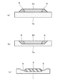
- (a)-(c) is a figure explaining the manufacturing method (manufacturing method A) of the ceramic multilayer substrate concerning the Example of this invention.
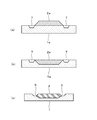
- (a)-(c) is a figure explaining the manufacturing method (manufacturing method B) of the ceramic multilayer substrate concerning the Example of this invention.
- (a)-(c) is a figure explaining the manufacturing method (manufacturing method C) of the ceramic multilayer substrate concerning the Example of this invention.
- (a)-(c) is a figure explaining the manufacturing method (manufacturing method D) of the ceramic multilayer substrate concerning the Example of this invention.
- (a)-(c) is a figure explaining the manufacturing method (manufacturing method E) of the ceramic multilayer substrate concerning the Example of this invention.
- FIG. 1 is a cross-sectional view schematically showing the overall configuration of a ceramic multilayer substrate 20 according to an embodiment of the present invention
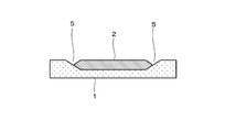
- FIG. 2 is a cross-sectional view showing the main part thereof.
- a ceramic multilayer substrate 20 is a ceramic multilayer substrate mounted on a mounting substrate, and includes a ceramic substrate 10 having a structure in which a plurality of ceramic layers (base ceramic layers) 1 are laminated, and a ceramic.
- a surface electrode 2 disposed on a ceramic layer 1 constituting the outermost layer of the substrate and an internal electrode 3 disposed on a predetermined ceramic layer 1 are provided.
- predetermined ones of the surface electrode 2 and the internal electrode 3 are connected to each other through a via-hole conductor 4.
- this ceramic multilayer substrate 20 As shown in FIGS. 1 and 2, between the surface electrode 2 and the surrounding ceramic layer 1 and between the internal electrode 3 and the surrounding ceramic layer 1.
- a recess 5 is provided.
- the recess 5 is formed by the surface electrode 2 and the surrounding ceramic layer 1 or by the internal electrode 3 and the surrounding ceramic layer 1. Since another ceramic layer 1 is laminated on the recess 5 formed by the internal electrode 3 and the surrounding ceramic layer 1, a gap is formed in the recess 5.
- the multilayer ceramic electronic component of Example 1 has the above-described configuration, and the concave portion 5 is provided between the surface electrode 2 and the internal electrode 3 and the surrounding ceramic layer 1. For example, it is possible to surely prevent a short circuit from occurring between adjacent electrodes due to bleeding or jumping out of the surface electrode 2 and the internal electrode 3. As a result, even when the distance between the electrodes such as the surface electrode 2 and the internal electrode 3 is narrowed (that is, the electrodes such as the surface electrode 2 and the internal electrode 3 are densified), there is no short-circuit between the electrodes and reliability. High ceramic multilayer substrate 20 can be obtained.
- each of the surface electrode and the internal electrode is configured to have a recess around the periphery, but the surface electrode formed on the surface of the ceramic substrate in which the electrodes are normally arranged at high density is used. Even when the concave portion is formed only around the periphery, a highly reliable ceramic multilayer substrate can be obtained.
- an electrode paste pattern 2a is formed by printing an electrode paste on the ceramic green sheet 1a.
- an electrode paste having a shrinkage rate (sintering shrinkage rate) in the firing process larger than that of the ceramic green sheet 1a is used as the electrode paste for forming the electrode paste pattern 2a.
- the ceramic green sheet 1a on which the electrode paste pattern 2a is printed is laminated and pressed to form a laminate.
- the electrode paste pattern 2a disposed on the ceramic green sheet 1a is pressed and deformed, and is buried in the ceramic green sheet 1a as schematically shown in FIG. 3 (b). It becomes.
- 3 (a) and 3 (b) show a ceramic green sheet 1a constituting the outermost layer of the laminate, and an electrode paste pattern 2a to be formed on the surface electrode 2 (see FIGS. 1 and 2) after firing.
- the electrode paste pattern that forms the internal electrode is similarly deformed to have a shape similar to the shape schematically shown in FIG.
- the sintering shrinkage rate is used as an electrode paste for forming an electrode paste pattern that becomes a surface electrode after firing.
- an electrode paste larger than the sintering shrinkage rate of the ceramic green sheet 1a may be used.
- the sintering shrinkage rate is used as an electrode paste for forming an electrode paste pattern that becomes an internal electrode after firing.
- an electrode paste larger than the sintering shrinkage rate of the ceramic green sheet 1a may be used.
- the ceramic material constituting the ceramic substrate and the constituent material and composition of the electrode paste it is necessary to appropriately select the ceramic material constituting the ceramic substrate and the constituent material and composition of the electrode paste, but specifically, it is actually used. It is desirable to appropriately select a ceramic material and additive components constituting the ceramic substrate, a conductive component constituting the electrode paste, an additive component such as glass, and the like in consideration of materials and characteristics required for the ceramic multilayer substrate. For example, if the ratio of the glass contained in the material constituting the ceramic substrate and the electrode paste is large, the glass component may ooze out and fill the recess, so it is usually preferable that the ratio of the glass component is small. .
- the electrode paste pattern 2a is formed by printing the electrode paste on the region surrounded by the resin paste 6 of the ceramic green sheet 1a.
- the ceramic green sheet 1a on which the electrode paste pattern 2a is formed is laminated and pressed to form a laminate.
- the electrode paste pattern 2a and the resin paste 6 disposed on the ceramic green sheet 1a are pressed and deformed, and as schematically shown in FIG. 4B, the ceramic green sheet 1a. It will be in the state buried in.
- FIGS. 1 and 2 show a ceramic green sheet 1a constituting the outermost layer of the laminate, and an electrode paste pattern 2a formed thereon and used as a surface electrode 2 (see FIGS. 1 and 2) after firing.
- the resin paste 6 is shown, the electrode paste pattern that forms the internal electrode and the resin paste disposed around the electrode paste pattern located inside the laminated body are also laminated and pressed in the same manner. It is deformed to have a shape similar to the shape schematically shown in FIG.
- an electrode paste pattern that becomes a surface electrode after firing is provided.
- the resin paste may be printed around the area where the electrode paste pattern is to be formed.
- an electrode paste pattern that becomes an internal electrode after firing is provided.
- the resin paste may be printed around the area where the electrode paste pattern is to be formed. Since another ceramic layer is formed on the concave portion formed around the internal electrode, a void is formed in the concave portion.
- grooves 7 are formed by laser processing around the area of the ceramic green sheet 1a where the electrode paste for electrode formation is printed.
- the electrode paste pattern 2a is formed by printing the electrode paste on the region surrounded by the groove 7 of the ceramic green sheet 1a.
- the electrode paste pattern 2a is printed on the inner region of the groove 7, the ceramic green sheet 1a is laminated, and the laminate is formed by pressure bonding. In this lamination and pressure bonding process, the electrode paste pattern 2a disposed on the ceramic green sheet 1a is pressed and deformed, and is embedded in the ceramic green sheet 1a as schematically shown in FIG. 5 (b). It becomes.
- FIGS. 1 and 2 show a ceramic green sheet 1a constituting the outermost layer of the laminate, and an electrode paste pattern 2a formed thereon and used as a surface electrode 2 (see FIGS. 1 and 2) after firing.
- the electrode paste pattern that forms the internal electrode is similarly deformed to have a shape similar to the shape schematically shown in FIG.
- the groove 7 is formed around the region of the ceramic green sheet 1a where the electrode paste for electrode formation is printed, and then the electrode paste is printed in the region surrounded by the groove 7 to form the electrode paste pattern 2a.
- the electrode paste pattern 2a is formed by printing the electrode paste on the ceramic green sheet 1a before forming the groove 7, and then the electrode paste of the ceramic green sheet 1a is formed. It is also possible to form the groove 7 around the area where the pattern 2a is formed.
- the groove 7 is formed after the electrode paste pattern 2a is formed, even if there is some oozing or popping out in the process of forming the electrode paste pattern 2a, it is removed in the process of forming the groove 7 Is done. As a result, even when surface electrodes and internal electrodes are arranged at high density at narrow intervals, a reliable ceramic multilayer substrate that is less likely to cause a short circuit between surface electrodes or between internal electrodes is reliably manufactured. It becomes possible to do.
- an electrode paste pattern that becomes a surface electrode after firing is provided.
- the groove may be formed only for the ceramic green sheet.
- an electrode paste pattern that becomes an internal electrode after firing is provided.
- the groove may be formed only for the ceramic green sheet. Since another ceramic layer is formed on the concave portion formed around the internal electrode, a void is formed in the concave portion.
- the electrode paste pattern 2a is formed by printing the electrode paste on the region surrounded by the resin paste 6 of the ceramic green sheet 1a.
- the ceramic green sheet on which the electrode paste pattern 2a to be the surface electrode 2 (see FIGS. 1 and 2) is formed, as shown in FIG. 6 (a), at least the peripheral portion of the electrode paste pattern 2a is provided.
- a coated ceramic green layer 8a that covers and does not cover the central portion is disposed.
- a ceramic paste is used, the resin paste 6 is covered from the peripheral portion of the electrode paste pattern 2a, and the ceramic paste is printed in a range reaching the exposed area of the ceramic green sheet 1a, thereby forming the coated ceramic green layer 8a.
- the ceramic used for the ceramic paste it is desirable to use a ceramic to which glass or an oxide is further added in order to increase the adhesion strength, centering on a ceramic having the same composition as that of the ceramic constituting the underlying ceramic substrate.
- the ceramic used for the ceramic paste may be a mixture of barium oxide, silicon oxide, alumina, calcium oxide, and boron oxide.
- the ceramic constituting the ceramic substrate serving as the base is a ferrite type, it is desirable to use ferrite powder.
- a method of laminating ceramic green sheets provided with an opening that exposes the central portion of the electrode paste pattern to be the surface electrode may be used. Is possible.
- a ceramic green sheet (not shown) provided with an electrode paste pattern to be an internal electrode is prepared by the same method as described in the manufacturing method B of [2] above.
- the ceramic green sheet 1a on which the coated ceramic green layer 8a is formed and the ceramic green sheet provided with the electrode paste pattern serving as an internal electrode are laminated and bonded to form a laminate.
- the electrode paste pattern 2a, the resin paste 6, and the coated ceramic green layer 8a disposed on the ceramic green sheet 1a are pressed and deformed, as schematically shown in FIG. 6 (b). In addition, it is buried in the ceramic green sheet 1a.
- the electrode paste pattern serving as an internal electrode has a shape as schematically shown in FIG. 4B used for explaining the manufacturing method B of [2] above.
- the laminate produced in the step (5) is fired.
- the resin paste 6 burns, decomposes and disappears, and as shown in FIG. 6C, a recess 5 is formed around the surface electrode 2 formed after firing, and the surface A ceramic multilayer substrate having a structure in which the peripheral edge of the electrode 2 is covered with the coated ceramic layer 8 obtained by firing the coated ceramic green layer 8a is obtained. Since the recess 5 formed by the surface electrode 2 and the surrounding ceramic layer 1 is covered with the coating ceramic layer 8, a gap is formed in the recess 5.
- the ceramic paste is not printed around the electrode paste pattern to be the internal electrode.
- the internal electrode is reliably covered between the ceramic layers, so that it is particularly covered. Even if the ceramic layer is not formed, the required reliability is ensured.
- the surface electrode 2 has a structure in which the peripheral portion of the surface electrode 2 is covered with the coating ceramic layer 8 and only the center portion of the surface electrode 2 is exposed. A ceramic multilayer substrate having an excellent peel strength of 2 is obtained.
- the electrode paste pattern 2a is formed by printing the electrode paste on the ceramic green sheet 1a.
- the ceramic green sheet 1a on which the electrode paste pattern 2a to be the surface electrode 2 (see FIGS. 1 and 2) is formed as shown in FIG. 7A, at least the periphery of the electrode paste pattern 2a A coated ceramic green layer 8a that covers the portion and does not cover the center portion is disposed.
- the coated ceramic green layer 8a is formed by printing the same ceramic paste as used in the manufacturing method D of [4] above.
- the electrode paste pattern 2a and the coated ceramic green layer 8a disposed on the ceramic green sheet 1a are pressed and deformed, and as shown schematically in FIG. It is buried in the sheet 1a, and the upper surface thereof is substantially flush with the upper surfaces of the surrounding ceramic green sheet 1a and the electrode paste pattern 2a.
- the electrode paste pattern 2a shrinks in the direction along the main surface, and as shown in FIG. 7C, between the surrounding ceramic layer (ceramic layer formed by firing the ceramic green sheet 1a) 1 Ceramic multilayer substrate having a structure in which a recess 5 is formed and a peripheral portion of the surface electrode 2 formed by firing the electrode paste pattern 2a is coated with the coated ceramic layer 8 formed by firing the coated ceramic green layer 8a Is obtained. Since the recess 5 formed by the surface electrode 2 and the surrounding ceramic layer 1 is covered with the coating ceramic layer 8, a gap is formed in the recess 5.
- the surface electrode 2 has a structure in which the peripheral edge portion of the surface electrode is covered with the covering ceramic layer 8 and only the central portion of the surface electrode 2 is exposed.
- a ceramic multilayer substrate having excellent peel strength can be obtained.
- the present invention is not limited to the above-described embodiments, and relates to a specific configuration of the ceramic substrate, an arrangement mode and constituent material of the internal electrode, a specific pattern of the surface electrode, and the like within the scope of the invention. It is possible to add various applications and modifications.
Landscapes
- Engineering & Computer Science (AREA)
- Manufacturing & Machinery (AREA)
- Microelectronics & Electronic Packaging (AREA)
- Chemical & Material Sciences (AREA)
- Ceramic Engineering (AREA)
- Inorganic Chemistry (AREA)
- Production Of Multi-Layered Print Wiring Board (AREA)
- Manufacturing Of Printed Wiring (AREA)
Abstract
L'invention concerne un procédé de fabrication d'un substrat multicouche en céramique et un substrat multicouche en céramique de haute fiabilité fabriqué à l'aide de ce procédé. Le procédé permet une fabrication efficace d'un substrat multicouche en céramique de haute fiabilité qui ne présente pas de court-circuit entre des électrodes adjacentes même si des électrodes de surface et des électrodes internes sont disposées avec une densité élevée. Un substrat multicouche en céramique (20) comporte un substrat en céramique (10) formé d'une pluralité de couches de céramique empilées (1) et des électrodes (électrodes de surface (2) et électrodes internes (3)) disposées dans les couches de céramique (1). Sur les surfaces principales de l'une quelconque des couches de céramique sont prévus des creux (5) constitués par les électrodes et la couche de céramique (1) entourant les électrodes. Les électrodes (électrodes de surface (2) et électrodes internes (3)) sont enfouies dans la couche de céramique (1). Les bords extérieurs des électrodes de surface (2) sont recouverts d'une couche de céramique de recouvrement.
Priority Applications (3)
| Application Number | Priority Date | Filing Date | Title |
|---|---|---|---|
| CN201280012049.8A CN103404241B (zh) | 2011-03-07 | 2012-03-02 | 陶瓷多层基板及其制造方法 |
| JP2013503500A JP5574038B2 (ja) | 2011-03-07 | 2012-03-02 | セラミック多層基板およびその製造方法 |
| US13/966,520 US9056442B2 (en) | 2011-03-07 | 2013-08-14 | Ceramic multilayer substrate and manufacturing method therefor |
Applications Claiming Priority (2)
| Application Number | Priority Date | Filing Date | Title |
|---|---|---|---|
| JP2011049044 | 2011-03-07 | ||
| JP2011-049044 | 2011-03-07 |
Related Child Applications (1)
| Application Number | Title | Priority Date | Filing Date |
|---|---|---|---|
| US13/966,520 Continuation US9056442B2 (en) | 2011-03-07 | 2013-08-14 | Ceramic multilayer substrate and manufacturing method therefor |
Publications (1)
| Publication Number | Publication Date |
|---|---|
| WO2012121141A1 true WO2012121141A1 (fr) | 2012-09-13 |
Family
ID=46798105
Family Applications (1)
| Application Number | Title | Priority Date | Filing Date |
|---|---|---|---|
| PCT/JP2012/055364 Ceased WO2012121141A1 (fr) | 2011-03-07 | 2012-03-02 | Substrat multicouche en céramique et son procédé de fabrication |
Country Status (3)
| Country | Link |
|---|---|
| US (1) | US9056442B2 (fr) |
| JP (1) | JP5574038B2 (fr) |
| WO (1) | WO2012121141A1 (fr) |
Cited By (12)
| Publication number | Priority date | Publication date | Assignee | Title |
|---|---|---|---|---|
| JPWO2012132880A1 (ja) * | 2011-03-25 | 2014-07-28 | 株式会社村田製作所 | セラミック多層基板 |
| CN104284531A (zh) * | 2013-07-04 | 2015-01-14 | 株式会社村田制作所 | 多层布线基板的制造方法、及具备利用该方法制造出的多层布线基板的探针卡、以及多层布线基板 |
| WO2015129600A1 (fr) * | 2014-02-26 | 2015-09-03 | 株式会社村田製作所 | Procédé de fabrication de substrat multicouche et substrat multicouche |
| JPWO2015151809A1 (ja) * | 2014-03-31 | 2017-04-13 | 株式会社村田製作所 | 積層配線基板およびこれを備えるプローブカード |
| WO2017199712A1 (fr) * | 2016-05-16 | 2017-11-23 | 株式会社村田製作所 | Composant électronique en céramique |
| WO2018216452A1 (fr) * | 2017-05-23 | 2018-11-29 | 株式会社村田製作所 | Composant électronique et procédé de fabrication de composant électronique |
| JP2022500868A (ja) * | 2018-09-14 | 2022-01-04 | ネーデルランドセ・オルガニサティ・フォール・トゥーヘパスト−ナトゥールウェテンスハッペライク・オンデルズーク・テーエヌオー | オブジェクトに印刷された導電性トラックを製造する方法及び3d印刷された電子機器 |
| WO2023084943A1 (fr) * | 2021-11-11 | 2023-05-19 | 株式会社村田製作所 | Composant électronique |
| JP2023091083A (ja) * | 2017-10-26 | 2023-06-29 | 京セラ株式会社 | 電子素子実装用基板、電子装置および電子モジュール |
| WO2024202648A1 (fr) * | 2023-03-28 | 2024-10-03 | 株式会社村田製作所 | Composant électronique |
| WO2025028029A1 (fr) * | 2023-07-31 | 2025-02-06 | 株式会社村田製作所 | Composant électronique en céramique |
| US12548709B2 (en) | 2020-11-26 | 2026-02-10 | Murata Manufacturing Co., Ltd. | Coil component |
Families Citing this family (4)
| Publication number | Priority date | Publication date | Assignee | Title |
|---|---|---|---|---|
| JP6583897B1 (ja) * | 2018-05-25 | 2019-10-02 | ▲らん▼海精研股▲ふん▼有限公司 | セラミック製静電チャックの製造方法 |
| WO2020241775A1 (fr) * | 2019-05-29 | 2020-12-03 | 京セラ株式会社 | Substrat de montage d'élément électronique, dispositif électronique et module électronique |
| DE102020201869A1 (de) | 2020-02-14 | 2021-08-19 | Robert Bosch Gesellschaft mit beschränkter Haftung | Schaltungsträger mit einer keramischen Lotstopp-Barriere |
| JP7438070B2 (ja) * | 2020-09-11 | 2024-02-26 | 新光電気工業株式会社 | 静電チャック、基板固定装置及び基板固定装置の製造方法 |
Citations (7)
| Publication number | Priority date | Publication date | Assignee | Title |
|---|---|---|---|---|
| JPH01236644A (ja) * | 1988-03-17 | 1989-09-21 | Toshiba Corp | 回路基板 |
| JPH024153B2 (fr) * | 1984-10-19 | 1990-01-26 | Intaanashonaru Bijinesu Mashiinzu Corp | |
| JPH04116892A (ja) * | 1990-09-06 | 1992-04-17 | Fujitsu Ltd | 多層セラミック基板およびその製造方法 |
| JPH04219993A (ja) * | 1990-12-20 | 1992-08-11 | Fujitsu Ltd | 多層セラミック基板およびその製造方法 |
| JP2006041017A (ja) * | 2004-07-23 | 2006-02-09 | Soshin Electric Co Ltd | 電子部品及び電子部品の製造方法 |
| JP2009164507A (ja) * | 2008-01-10 | 2009-07-23 | Seiko Epson Corp | セラミック多層基板及びセラミック多層基板の製造方法 |
| JP2009170683A (ja) * | 2008-01-17 | 2009-07-30 | Seiko Epson Corp | 多層基板の製造方法 |
Family Cites Families (4)
| Publication number | Priority date | Publication date | Assignee | Title |
|---|---|---|---|---|
| JPH09260540A (ja) | 1996-03-27 | 1997-10-03 | Toshiba Corp | 半導体用パッケージ基体の製造方法 |
| JP2003151351A (ja) | 2001-08-30 | 2003-05-23 | Kyocera Corp | 導電性ペースト及びセラミック回路基板の製法 |
| JP2010166018A (ja) | 2008-12-16 | 2010-07-29 | Seiko Instruments Inc | 電子部品およびその製造方法 |
| WO2012132880A1 (fr) * | 2011-03-25 | 2012-10-04 | 株式会社村田製作所 | Substrat céramique multicouche |
-
2012
- 2012-03-02 WO PCT/JP2012/055364 patent/WO2012121141A1/fr not_active Ceased
- 2012-03-02 JP JP2013503500A patent/JP5574038B2/ja active Active
-
2013
- 2013-08-14 US US13/966,520 patent/US9056442B2/en active Active
Patent Citations (7)
| Publication number | Priority date | Publication date | Assignee | Title |
|---|---|---|---|---|
| JPH024153B2 (fr) * | 1984-10-19 | 1990-01-26 | Intaanashonaru Bijinesu Mashiinzu Corp | |
| JPH01236644A (ja) * | 1988-03-17 | 1989-09-21 | Toshiba Corp | 回路基板 |
| JPH04116892A (ja) * | 1990-09-06 | 1992-04-17 | Fujitsu Ltd | 多層セラミック基板およびその製造方法 |
| JPH04219993A (ja) * | 1990-12-20 | 1992-08-11 | Fujitsu Ltd | 多層セラミック基板およびその製造方法 |
| JP2006041017A (ja) * | 2004-07-23 | 2006-02-09 | Soshin Electric Co Ltd | 電子部品及び電子部品の製造方法 |
| JP2009164507A (ja) * | 2008-01-10 | 2009-07-23 | Seiko Epson Corp | セラミック多層基板及びセラミック多層基板の製造方法 |
| JP2009170683A (ja) * | 2008-01-17 | 2009-07-30 | Seiko Epson Corp | 多層基板の製造方法 |
Cited By (27)
| Publication number | Priority date | Publication date | Assignee | Title |
|---|---|---|---|---|
| JPWO2012132880A1 (ja) * | 2011-03-25 | 2014-07-28 | 株式会社村田製作所 | セラミック多層基板 |
| CN104284531A (zh) * | 2013-07-04 | 2015-01-14 | 株式会社村田制作所 | 多层布线基板的制造方法、及具备利用该方法制造出的多层布线基板的探针卡、以及多层布线基板 |
| JP2015015339A (ja) * | 2013-07-04 | 2015-01-22 | 株式会社村田製作所 | 多層配線基板の製造方法およびこの方法により製造される多層配線基板を備えるプローブカード並びに多層配線基板 |
| US9523709B2 (en) | 2013-07-04 | 2016-12-20 | Murata Manufcaturing Co., Ltd. | Method of manufacturing multilayer wiring board, probe card including multilayer wiring board manufactured by the method, and multilayer wiring board |
| US10051730B2 (en) | 2014-02-26 | 2018-08-14 | Murata Manufacturing Co., Ltd. | Multilayer substrate manufacturing method and multilayer substrate |
| WO2015129600A1 (fr) * | 2014-02-26 | 2015-09-03 | 株式会社村田製作所 | Procédé de fabrication de substrat multicouche et substrat multicouche |
| JP5880802B1 (ja) * | 2014-02-26 | 2016-03-09 | 株式会社村田製作所 | 多層基板の製造方法、及び多層基板 |
| JPWO2015151809A1 (ja) * | 2014-03-31 | 2017-04-13 | 株式会社村田製作所 | 積層配線基板およびこれを備えるプローブカード |
| US10729009B2 (en) | 2016-05-16 | 2020-07-28 | Murata Manufacturing Co., Ltd. | Ceramic electronic component |
| US11641712B2 (en) | 2016-05-16 | 2023-05-02 | Murata Manufacturing Co., Ltd. | Ceramic electronic component |
| JPWO2017199712A1 (ja) * | 2016-05-16 | 2019-02-14 | 株式会社村田製作所 | セラミック電子部品 |
| US11647581B2 (en) | 2016-05-16 | 2023-05-09 | Murata Manufacturing Co., Ltd. | Ceramic electronic component |
| WO2017199712A1 (fr) * | 2016-05-16 | 2017-11-23 | 株式会社村田製作所 | Composant électronique en céramique |
| JP2021141341A (ja) * | 2017-05-23 | 2021-09-16 | 株式会社村田製作所 | 電子部品 |
| JPWO2018216452A1 (ja) * | 2017-05-23 | 2020-03-12 | 株式会社村田製作所 | 電子部品、及び、電子部品の製造方法 |
| JP7131658B2 (ja) | 2017-05-23 | 2022-09-06 | 株式会社村田製作所 | 電子部品 |
| US11450483B2 (en) | 2017-05-23 | 2022-09-20 | Murata Manufacturing Co., Ltd. | Electronic component with baked electrodes and having a continuously curved recess |
| WO2018216452A1 (fr) * | 2017-05-23 | 2018-11-29 | 株式会社村田製作所 | Composant électronique et procédé de fabrication de composant électronique |
| JP2023091083A (ja) * | 2017-10-26 | 2023-06-29 | 京セラ株式会社 | 電子素子実装用基板、電子装置および電子モジュール |
| JP7569885B2 (ja) | 2017-10-26 | 2024-10-18 | 京セラ株式会社 | 電子素子実装用基板、電子装置および電子モジュール |
| JP2022500868A (ja) * | 2018-09-14 | 2022-01-04 | ネーデルランドセ・オルガニサティ・フォール・トゥーヘパスト−ナトゥールウェテンスハッペライク・オンデルズーク・テーエヌオー | オブジェクトに印刷された導電性トラックを製造する方法及び3d印刷された電子機器 |
| US11825610B2 (en) | 2018-09-14 | 2023-11-21 | Nederlandse Organisatie Voor Toegepast-Natuurwetenschappelijk Onderzoek Tno | Process for the manufacturing of printed conductive tracks on an object and 3D printed electronics |
| JP7401533B2 (ja) | 2018-09-14 | 2023-12-19 | ネーデルランドセ・オルガニサティ・フォール・トゥーヘパスト-ナトゥールウェテンスハッペライク・オンデルズーク・テーエヌオー | オブジェクトに印刷された導電性トラックを製造する方法及び3d印刷された電子機器 |
| US12548709B2 (en) | 2020-11-26 | 2026-02-10 | Murata Manufacturing Co., Ltd. | Coil component |
| WO2023084943A1 (fr) * | 2021-11-11 | 2023-05-19 | 株式会社村田製作所 | Composant électronique |
| WO2024202648A1 (fr) * | 2023-03-28 | 2024-10-03 | 株式会社村田製作所 | Composant électronique |
| WO2025028029A1 (fr) * | 2023-07-31 | 2025-02-06 | 株式会社村田製作所 | Composant électronique en céramique |
Also Published As
| Publication number | Publication date |
|---|---|
| JPWO2012121141A1 (ja) | 2014-07-17 |
| JP5574038B2 (ja) | 2014-08-20 |
| US20130330509A1 (en) | 2013-12-12 |
| CN103404241A (zh) | 2013-11-20 |
| US9056442B2 (en) | 2015-06-16 |
Similar Documents
| Publication | Publication Date | Title |
|---|---|---|
| JP5574038B2 (ja) | セラミック多層基板およびその製造方法 | |
| KR101659146B1 (ko) | 기판 내장용 적층 세라믹 전자부품 및 적층 세라믹 전자부품 내장형 인쇄회로기판 | |
| KR102093157B1 (ko) | 다층 세라믹 기판 | |
| JP2014123707A (ja) | 基板内蔵用積層セラミック電子部品及びその製造方法、並びに基板内蔵用積層セラミック電子部品を備えるプリント基板 | |
| JP5835282B2 (ja) | 多層配線基板の製造方法およびプローブカードの製造方法並びに多層配線基板およびプローブカード | |
| JPWO2012157436A1 (ja) | セラミック電子部品およびその製造方法 | |
| JP2003246680A (ja) | 多層セラミック基板の製造方法 | |
| KR101805074B1 (ko) | 세라믹 다층회로 기판의 제조방법 | |
| JP3956703B2 (ja) | 積層型セラミック電子部品の製造方法 | |
| JP4965237B2 (ja) | 配線基板内蔵用コンデンサ及び配線基板 | |
| TWI749872B (zh) | 陶瓷配線基板及陶瓷配線基板的製造方法 | |
| CN103404241B (zh) | 陶瓷多层基板及其制造方法 | |
| KR101018100B1 (ko) | 다층 세라믹 기판, 다중 전극을 갖는 도전성 비아 형성 방법 및 이를 이용한 다층 세라믹 기판의 제조방법 | |
| JP2012089818A (ja) | 積層型セラミック電子部品の製造方法 | |
| JP5724806B2 (ja) | セラミック多層基板及びその製造方法 | |
| JP2010187011A (ja) | 積層型セラミック電子部品 | |
| JP4746423B2 (ja) | 配線基板内蔵用コンデンサの製造方法及び配線基板内蔵用コンデンサ | |
| JP2007165540A (ja) | 多層セラミック基板の製造方法及び多層セラミック集合基板 | |
| JP4550774B2 (ja) | 配線基板内蔵用コンデンサ、配線基板、積層体、コンデンサ集合体、配線基板内蔵用コンデンサ製造方法 | |
| JP2004095753A (ja) | 多層セラミック基板の製造方法 | |
| JP2010225707A (ja) | セラミック多層基板及びその製造方法 | |
| JP4548612B2 (ja) | 積層セラミック電子部品の製造方法 | |
| JP2013165086A (ja) | セラミック多層基板とセラミック多層基板の製造方法 | |
| JP2011071355A (ja) | セラミック多層基板の製造方法 | |
| JP2006229093A (ja) | ガラスセラミック基板の製造方法 |
Legal Events
| Date | Code | Title | Description |
|---|---|---|---|
| 121 | Ep: the epo has been informed by wipo that ep was designated in this application |
Ref document number: 12755319 Country of ref document: EP Kind code of ref document: A1 |
|
| ENP | Entry into the national phase |
Ref document number: 2013503500 Country of ref document: JP Kind code of ref document: A |
|
| NENP | Non-entry into the national phase |
Ref country code: DE |
|
| 122 | Ep: pct application non-entry in european phase |
Ref document number: 12755319 Country of ref document: EP Kind code of ref document: A1 |