WO2012124362A1 - Substrat multicouche en résine - Google Patents
Substrat multicouche en résine Download PDFInfo
- Publication number
- WO2012124362A1 WO2012124362A1 PCT/JP2012/050672 JP2012050672W WO2012124362A1 WO 2012124362 A1 WO2012124362 A1 WO 2012124362A1 JP 2012050672 W JP2012050672 W JP 2012050672W WO 2012124362 A1 WO2012124362 A1 WO 2012124362A1
- Authority
- WO
- WIPO (PCT)
- Prior art keywords
- surface electrode
- conductor pattern
- plane conductor
- resin multilayer
- substrate body
- Prior art date
- Legal status (The legal status is an assumption and is not a legal conclusion. Google has not performed a legal analysis and makes no representation as to the accuracy of the status listed.)
- Ceased
Links
Images



Classifications
-
- H—ELECTRICITY
- H05—ELECTRIC TECHNIQUES NOT OTHERWISE PROVIDED FOR
- H05K—PRINTED CIRCUITS; CASINGS OR CONSTRUCTIONAL DETAILS OF ELECTRIC APPARATUS; MANUFACTURE OF ASSEMBLAGES OF ELECTRICAL COMPONENTS
- H05K1/00—Printed circuits
- H05K1/02—Details
- H05K1/11—Printed elements for providing electric connections to or between printed circuits
- H05K1/115—Via connections; Lands around holes or via connections
- H05K1/116—Lands, clearance holes or other lay-out details concerning the surrounding of a via
-
- H—ELECTRICITY
- H05—ELECTRIC TECHNIQUES NOT OTHERWISE PROVIDED FOR
- H05K—PRINTED CIRCUITS; CASINGS OR CONSTRUCTIONAL DETAILS OF ELECTRIC APPARATUS; MANUFACTURE OF ASSEMBLAGES OF ELECTRICAL COMPONENTS
- H05K3/00—Apparatus or processes for manufacturing printed circuits
- H05K3/46—Manufacturing multilayer circuits
- H05K3/4611—Manufacturing multilayer circuits by laminating two or more circuit boards
- H05K3/4626—Manufacturing multilayer circuits by laminating two or more circuit boards characterised by the insulating layers or materials
- H05K3/4632—Manufacturing multilayer circuits by laminating two or more circuit boards characterised by the insulating layers or materials laminating thermoplastic or uncured resin sheets comprising printed circuits without added adhesive materials between the sheets
-
- H—ELECTRICITY
- H05—ELECTRIC TECHNIQUES NOT OTHERWISE PROVIDED FOR
- H05K—PRINTED CIRCUITS; CASINGS OR CONSTRUCTIONAL DETAILS OF ELECTRIC APPARATUS; MANUFACTURE OF ASSEMBLAGES OF ELECTRICAL COMPONENTS
- H05K2201/00—Indexing scheme relating to printed circuits covered by H05K1/00
- H05K2201/01—Dielectrics
- H05K2201/0104—Properties and characteristics in general
- H05K2201/0129—Thermoplastic polymer, e.g. auto-adhesive layer; Shaping of thermoplastic polymer
-
- H—ELECTRICITY
- H05—ELECTRIC TECHNIQUES NOT OTHERWISE PROVIDED FOR
- H05K—PRINTED CIRCUITS; CASINGS OR CONSTRUCTIONAL DETAILS OF ELECTRIC APPARATUS; MANUFACTURE OF ASSEMBLAGES OF ELECTRICAL COMPONENTS
- H05K2201/00—Indexing scheme relating to printed circuits covered by H05K1/00
- H05K2201/09—Shape and layout
- H05K2201/09209—Shape and layout details of conductors
- H05K2201/09372—Pads and lands
- H05K2201/09427—Special relation between the location or dimension of a pad or land and the location or dimension of a terminal
-
- H—ELECTRICITY
- H05—ELECTRIC TECHNIQUES NOT OTHERWISE PROVIDED FOR
- H05K—PRINTED CIRCUITS; CASINGS OR CONSTRUCTIONAL DETAILS OF ELECTRIC APPARATUS; MANUFACTURE OF ASSEMBLAGES OF ELECTRICAL COMPONENTS
- H05K2201/00—Indexing scheme relating to printed circuits covered by H05K1/00
- H05K2201/09—Shape and layout
- H05K2201/09209—Shape and layout details of conductors
- H05K2201/09372—Pads and lands
- H05K2201/09481—Via in pad; Pad over filled via
-
- H—ELECTRICITY
- H05—ELECTRIC TECHNIQUES NOT OTHERWISE PROVIDED FOR
- H05K—PRINTED CIRCUITS; CASINGS OR CONSTRUCTIONAL DETAILS OF ELECTRIC APPARATUS; MANUFACTURE OF ASSEMBLAGES OF ELECTRICAL COMPONENTS
- H05K2201/00—Indexing scheme relating to printed circuits covered by H05K1/00
- H05K2201/09—Shape and layout
- H05K2201/09209—Shape and layout details of conductors
- H05K2201/095—Conductive through-holes or vias
- H05K2201/09509—Blind vias, i.e. vias having one side closed
- H05K2201/09527—Inverse blind vias, i.e. bottoms outwards in multilayer PCB; Blind vias in centre of PCB having opposed bottoms
-
- H—ELECTRICITY
- H05—ELECTRIC TECHNIQUES NOT OTHERWISE PROVIDED FOR
- H05K—PRINTED CIRCUITS; CASINGS OR CONSTRUCTIONAL DETAILS OF ELECTRIC APPARATUS; MANUFACTURE OF ASSEMBLAGES OF ELECTRICAL COMPONENTS
- H05K2201/00—Indexing scheme relating to printed circuits covered by H05K1/00
- H05K2201/09—Shape and layout
- H05K2201/09209—Shape and layout details of conductors
- H05K2201/095—Conductive through-holes or vias
- H05K2201/096—Vertically aligned vias, holes or stacked vias
-
- H—ELECTRICITY
- H05—ELECTRIC TECHNIQUES NOT OTHERWISE PROVIDED FOR
- H05K—PRINTED CIRCUITS; CASINGS OR CONSTRUCTIONAL DETAILS OF ELECTRIC APPARATUS; MANUFACTURE OF ASSEMBLAGES OF ELECTRICAL COMPONENTS
- H05K2201/00—Indexing scheme relating to printed circuits covered by H05K1/00
- H05K2201/09—Shape and layout
- H05K2201/09209—Shape and layout details of conductors
- H05K2201/09654—Shape and layout details of conductors covering at least two types of conductors provided for in H05K2201/09218 - H05K2201/095
- H05K2201/09781—Dummy conductors, i.e. not used for normal transport of current; Dummy electrodes of components
-
- H—ELECTRICITY
- H05—ELECTRIC TECHNIQUES NOT OTHERWISE PROVIDED FOR
- H05K—PRINTED CIRCUITS; CASINGS OR CONSTRUCTIONAL DETAILS OF ELECTRIC APPARATUS; MANUFACTURE OF ASSEMBLAGES OF ELECTRICAL COMPONENTS
- H05K3/00—Apparatus or processes for manufacturing printed circuits
- H05K3/46—Manufacturing multilayer circuits
- H05K3/4611—Manufacturing multilayer circuits by laminating two or more circuit boards
- H05K3/4614—Manufacturing multilayer circuits by laminating two or more circuit boards the electrical connections between the circuit boards being made during lamination
- H05K3/4617—Manufacturing multilayer circuits by laminating two or more circuit boards the electrical connections between the circuit boards being made during lamination characterized by laminating only or mainly similar single-sided circuit boards
Definitions
- the present invention relates to a resin multilayer substrate, and more particularly to a resin multilayer substrate including a substrate body on which an insulating layer made of a resin material is laminated.
- 121b are laminated and pressure-bonded while being heated to produce the resin multilayer substrate 100.
- the interlayer connection conductor 151 is connected to the surface electrode formed by the conductor pattern 122 exposed on the mounting surface 160 of the substrate body 139 in which the pattern films 121, 121 a, 121 b are integrated by heat fusion.
- the resin multilayer substrate Since the resin multilayer substrate has flexibility, it can be used as a flexible substrate. However, when the resin multilayer substrate is bent and used, the surface electrode is easily peeled off from the substrate body.
- the present invention intends to provide a resin multilayer substrate capable of suppressing the peeling of the surface electrode from the substrate body.
- the present invention provides a resin multilayer substrate configured as follows.
- the resin multilayer substrate includes: (a) a substrate body on which an insulating layer made of a resin material is laminated; (b) a surface electrode formed on one main surface of the substrate body; and (c) the insulating layers adjacent to each other. And an in-plane conductor pattern facing the surface electrode.
- the in-plane conductor pattern overlaps with the surface electrode and protrudes outside the surface electrode with an interval over the entire circumference of the surface electrode when seen through from the stacking direction in which the insulating layers are stacked.
- the surface electrode faces the in-plane conductor pattern larger than the surface electrode
- the surface electrode and the surface electrode The resin material of the insulating layer sandwiched between the in-plane conductive patterns facing the electrodes has no escape in the stacking direction. Therefore, the pressure acting on the interface between the surface electrode and the insulating layer is increased. Thereby, the bonding between the surface electrode and the insulating layer can be strengthened, and peeling of the surface electrode from the substrate body can be suppressed.
- an interlayer connection conductor that penetrates the insulating layer and connects the surface electrode and the in-plane conductor pattern is provided.
- the portion where the surface electrode and the in-plane conductor pattern are connected via the interlayer connection conductor is formed of a conductive metal or the like, and is less likely to deform than the resin material of the insulating layer. Therefore, when bending deformation occurs in the substrate body, the deformation of the insulating layer around the surface electrode is constrained, and the substrate body is less deformed in the vicinity of the surface electrode. Thereby, peeling of the surface electrode from the substrate body can be suppressed.
- a slit is formed in the in-plane conductor pattern.
- the insulating layers arranged on both sides of the in-plane conductor pattern in which the slit is formed are joined to each other through the slit formed in the in-plane conductor pattern.
- a through hole is formed in the in-plane conductor pattern.
- the insulating layers arranged on both sides of the in-plane conductor pattern in which the through hole is formed are joined to each other through the through hole formed in the in-plane conductor pattern.
- only the insulating layer or only the interlayer connection conductor and the insulating layer are disposed between the surface electrode and the in-plane conductor pattern.
- the distance between the surface electrode and the in-plane conductor pattern can be shortened to further suppress deformation in the vicinity of the surface electrode and further suppress peeling of the surface electrode from the substrate body.
- a back electrode formed on the other main surface of the substrate body is further provided opposite to the front electrode.
- the interlayer connection conductor is connected to the back electrode.
- the portion where the front surface electrode, the back surface electrode, and the interlayer connection conductor are connected is formed of a conductive metal or the like and is less likely to be deformed than the insulating layer of the resin material.
- peeling of the surface electrode from the substrate body can be suppressed.
- Example 1 It is sectional drawing of a resin multilayer substrate.
- Example 1 It is principal part sectional drawing of a resin multilayer substrate.
- Example 1 It is sectional drawing which shows the manufacturing process of a resin multilayer substrate.
- Example 1 It is sectional drawing which shows the manufacturing process of a resin multilayer substrate.
- Example 1 It is sectional drawing of a resin multilayer substrate.
- Example 2 It is principal part sectional drawing of a resin multilayer substrate.
- Example 2 It is principal part sectional drawing of a resin multilayer substrate.
- (Modification) It is sectional drawing which shows the manufacturing process of a resin multilayer substrate. (Conventional example)
- Example 1 The resin multilayer substrate 10 of Example 1 will be described with reference to FIGS.
- FIG. 1 is a cross-sectional view of the resin multilayer substrate 10.
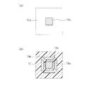
- FIG. 2A is a cross-sectional view of the principal part taken along line AA in FIG.
- FIG. 2B is a cross-sectional view of the main part taken along line BB in FIG.
- the resin multilayer substrate 10 has a surface electrode 18 a formed on one main surface 12 a of a substrate body 12 on which an insulating layer made of a resin material is laminated, and the other main surface of the substrate body 12.
- a back electrode 18b is formed on the surface 12b.
- one of the front electrode 18a and the back electrode 18b is used as an external electrode for mounting the resin multilayer substrate 10 on another circuit board or the like, and the other is for mounting an electronic component on the resin multilayer substrate 10. Used as a land electrode.
- in-plane conductor patterns 14, 14a, 14b disposed between adjacent insulating layers of the substrate body 12 and an interlayer connection conductor 16 penetrating the insulating layer are formed.
- the in-plane conductor pattern 14a facing the surface electrode 18a overlaps with the surface electrode 18a and is spaced over the entire circumference of the surface electrode 18a when viewed from the stacking direction in which the insulating layers are stacked. And protrudes outside the surface electrode 18a.
- the in-plane conductor pattern 14a is larger than the surface electrode 18a.
- the surface electrode 18a is opposed to the in-plane conductor pattern 14a larger than the surface electrode 18a, when the insulating layer made of the resin material is pressure-bonded in the step of manufacturing the resin multilayer substrate 10, the surface electrode The resin material of the insulating layer sandwiched between 18a and the in-plane conductor pattern 14a facing the surface electrode 18a has no escape in the stacking direction. Therefore, the pressure acting on the interface between the surface electrode 18a and the insulating layer is increased. Thereby, the bonding between the surface electrode 18a and the insulating layer can be strengthened, and the peeling of the surface electrode 18a from the substrate body 12 can be suppressed.
- the portion where the surface electrode 18a and the in-plane conductor pattern 14a are connected via the interlayer connection conductor 16 is formed of a conductive metal or the like, and is less likely to be deformed than the resin material of the insulating layer. For this reason, when bending deformation occurs in the substrate body 12, the deformation of the insulating layer around the surface electrode 18a is constrained, and the substrate body 12 is less deformed in the vicinity of the surface electrode 18a. Thereby, peeling of the surface electrode 18a from the substrate body 12 can be suppressed.
- the in-plane conductor pattern 14b facing the back electrode 18b overlaps with the back electrode 18b when seen through from the stacking direction in which the insulating layers are stacked, and the back electrode 18b. Are spaced outside the back electrode 18b with a space around the entire circumference.
- the in-plane conductor pattern 14b is larger than the back electrode 18b.
- the interlayer connection conductor 16 is connected to the front surface electrode 18a, the in-plane conductor patterns 14, 14a, 14b, and the back surface electrode 18b, penetrates the substrate body 12, and is formed in a column shape.
- the portion where the interlayer connection conductor 16 is connected to the front surface electrode 18a and the back surface electrode 18b is formed of a conductive metal or the like and is less likely to be deformed than an insulating layer of a resin material. To do. Thereby, since the deformation
- FIGS. 3 and 4 are cross-sectional views showing the manufacturing steps of the resin multilayer substrate 10.
- a resin sheet 11 for forming the substrate body 12 is prepared.
- LCP liquid crystal polymer
- PPS polyphenylene
- a metal foil 13 such as Cu, Ag, Sn, Ni, Au or an alloy thereof is attached to one main surface 11t.
- a resin sheet 11 made of a thermoplastic resin material such as sulfide), PEEK (polyetheretherketone), or PI (polyimide) is prepared.
- the other main surface 11s side of the resin sheet 11 is prepared.
- a through hole (via hole) 11p reaching the metal foil 13 is formed by a method such as laser processing.
- the mask pattern 2 is formed on the metal foil 13 so as to cover the position corresponding to the through hole 11p, for example, by applying a photoresist, exposing, and developing. After etching the metal foil 13 as shown in FIG. 3D, the mask pattern 2 is removed as shown in FIG. As a result, portions that become the in-plane conductor patterns 14, 14a, 14b are formed.
- the via-hole conductor 15 is formed by filling the through hole 11p with a conductive paste by a method such as screen printing.
- the resin sheets 11a to 11f that become the insulating layers of the substrate body 12 are laminated in a predetermined direction to form a laminate 11x.
- the laminated body 11x is pressure-bonded while heating to form the substrate body 12.
- the via-hole conductor 15 is cured and the interlayer connection conductor 16 is formed.
- the resin multilayer substrate 10 can be manufactured.
- Example 2 The resin multilayer substrate 10a of Example 2 will be described with reference to FIGS.
- FIG. 5 is a cross-sectional view of the resin multilayer substrate 10a.
- FIG. 6A is a cross-sectional view of the principal part taken along line AA in FIG.
- FIG. 6B is a cross-sectional view of the principal part taken along line BB in FIG.
- the resin multilayer substrate 10a of Example 2 is configured in substantially the same manner as the resin multilayer substrate 10 of Example 1.
- the same reference numerals are used for the same components as in the first embodiment, and differences from the first embodiment will be mainly described.
- the in-plane conductor pattern 14s facing the surface electrode 18a overlaps with the surface electrode 18a when seen through from the stacking direction in which the insulating layers are stacked, as in the first embodiment.
- the electrode 18a protrudes outward from the surface electrode 18a with an interval around the entire circumference.
- the in-plane conductor pattern 14s is larger than the surface electrode 18a.
- a slit 14m is formed in the in-plane conductor pattern 14s facing the surface electrode 18a.
- the slit 14m is formed so as to communicate with the corner of the in-plane conductor pattern 14s and surround the outer surface of the surface electrode 18a when seen through from the stacking direction in which the insulating layers are stacked.
- the slit 14m can be formed so as to partially overlap the surface electrode 18a when seen through from the stacking direction. However, if the slit 14m is formed so as not to overlap the surface electrode 18a, the slit 14m It is preferable because the pressure is difficult to escape from the slit 14m, the pressure acting between the surface electrode 18a and the insulating layer can be increased, and the bonding between the surface electrode 18a and the insulating layer can be strengthened.
- the insulating layers arranged on both sides of the in-plane conductor pattern 14s where the slit 14m is formed and sandwiching the in-plane conductor pattern 14s are joined via the slit 14m of the in-plane conductor pattern 14s.
- the in-plane conductor pattern 14t facing the back electrode 18b is configured in the same manner as the in-plane conductor pattern 14s facing the front electrode 18a.
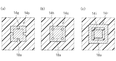
- FIG. 7 is a cross-sectional view of an essential part showing in-plane conductor patterns 14p to 14r of a modification facing the surface electrode 18a.
- the cross-sectional view of FIG. 7 is a cross-sectional view of the main part similar to FIG. 6B, and any of the in-plane conductor patterns 14p to 14r overlaps with the surface electrode 18a when seen through from the stacking direction in which the insulating layers are stacked. In addition, the entire surface of the surface electrode 18a is spaced apart from the surface electrode 18a.
- a slit 14g is formed in the middle of each side. 7A, the slit 11g does not reach the surface electrode 18a when seen through from the stacking direction in which the insulating layers are stacked. However, the slit 11g may be formed so as to be in contact with or overlap the surface electrode 18a. It is.
- the insulating layers which are arranged on both sides of the in-plane conductor pattern 14p where the slit 14g is formed and sandwich the in-plane conductor pattern 14p are joined through the slit 14g of the in-plane conductor pattern 14p.
- a through-hole 14h is formed in the in-plane conductor pattern 14q shown in FIG. FIG. 7B illustrates a case where a part of the through hole 14h overlaps the surface electrode 18a when seen through from the stacking direction in which the insulating layers are stacked, but the entire through hole 14h overlaps the surface electrode 18a.
- the insulating layers that are disposed on both sides of the in-plane conductor pattern 14q in which the through-hole 14h is formed and sandwich the in-plane conductor pattern 14q are joined via the through-hole 14h formed in the in-plane conductor pattern 14q, Bonding between the in-plane conductor pattern 14q and the insulating layers on both sides thereof can be strengthened, and peeling of the in-plane conductor pattern 14q inside the substrate body can be suppressed.
- the in-plane conductor pattern 14r shown in FIG. 7C has a rectangular through hole 14i.
- the through-hole 14i is formed so as to surround the outer surface of the surface electrode 18a when viewed from the stacking direction in which the insulating layers are stacked. However, the through-hole 14i is formed so that part or all of the through-hole overlaps the surface electrode 18a. Is also possible.
- the insulating layers that are disposed on both sides of the in-plane conductor pattern 14r in which the through-hole 14i is formed and sandwich the in-plane conductor pattern 14r are joined through the through-hole 14i formed in the in-plane conductor pattern 14r, Bonding between the in-plane conductor pattern 14r and the insulating layers on both sides thereof can be strengthened, and peeling of the in-plane conductor pattern 14r inside the substrate body can be suppressed.
- the back electrode may be omitted.
Landscapes
- Engineering & Computer Science (AREA)
- Microelectronics & Electronic Packaging (AREA)
- Manufacturing & Machinery (AREA)
- Production Of Multi-Layered Print Wiring Board (AREA)
- Measurement Of Radiation (AREA)
Abstract
L'invention porte sur un substrat multicouche en résine, avec lequel le décollement d'électrodes de surface d'un corps de substrat peut être inhibé. Le substrat multicouche en résine est doté de : (a) un corps de substrat (12) qui a des couches isolantes comprenant de la matière de type résine stratifiée ; (b) des électrodes de surface (18a) qui sont formées sur une face principale (12a) du corps de substrat (12) ; et (c) des motifs de conducteur dans le plan (14a) qui sont disposés entre des couches isolantes adjacentes et qui sont à l'opposé des électrodes de surface (18a). Les motifs de conducteur dans le plan (14a) se superposent aux électrodes de surface (18a), lorsqu'ils sont observés en transparence dans la direction où les couches isolantes sont stratifiées, et s'étendent vers l'extérieur de la circonférence externe des électrodes de surface (18a) le long de toute la circonférence de celles-ci, avec un espace intercalé entre eux.
Priority Applications (2)
| Application Number | Priority Date | Filing Date | Title |
|---|---|---|---|
| JP2013504584A JP5741975B2 (ja) | 2011-03-17 | 2012-01-16 | 樹脂多層基板 |
| CN201280013474.9A CN103430639B (zh) | 2011-03-17 | 2012-01-16 | 树脂多层基板 |
Applications Claiming Priority (2)
| Application Number | Priority Date | Filing Date | Title |
|---|---|---|---|
| JP2011059319 | 2011-03-17 | ||
| JP2011-059319 | 2011-03-17 |
Publications (1)
| Publication Number | Publication Date |
|---|---|
| WO2012124362A1 true WO2012124362A1 (fr) | 2012-09-20 |
Family
ID=46830443
Family Applications (1)
| Application Number | Title | Priority Date | Filing Date |
|---|---|---|---|
| PCT/JP2012/050672 Ceased WO2012124362A1 (fr) | 2011-03-17 | 2012-01-16 | Substrat multicouche en résine |
Country Status (3)
| Country | Link |
|---|---|
| JP (1) | JP5741975B2 (fr) |
| CN (1) | CN103430639B (fr) |
| WO (1) | WO2012124362A1 (fr) |
Cited By (4)
| Publication number | Priority date | Publication date | Assignee | Title |
|---|---|---|---|---|
| WO2015151809A1 (fr) * | 2014-03-31 | 2015-10-08 | 株式会社村田製作所 | Carte de câblage stratifiée et carte sonde la comprenant |
| JPWO2016052284A1 (ja) * | 2014-09-30 | 2017-06-22 | 株式会社村田製作所 | 多層基板 |
| WO2021206019A1 (fr) * | 2020-04-07 | 2021-10-14 | 株式会社村田製作所 | Substrat multicouche et son procédé de fabrication |
| JPWO2021246467A1 (fr) * | 2020-06-03 | 2021-12-09 |
Citations (4)
| Publication number | Priority date | Publication date | Assignee | Title |
|---|---|---|---|---|
| JPS63136596A (ja) * | 1986-11-27 | 1988-06-08 | イビデン株式会社 | 多層プリント配線板 |
| JP2000277912A (ja) * | 1999-03-29 | 2000-10-06 | Clover Denshi Kogyo Kk | 多層プリント配線基板の製造方法 |
| JP2002290047A (ja) * | 2001-03-23 | 2002-10-04 | Denso Corp | プリント基板の製造方法 |
| JP2003078249A (ja) * | 2001-09-06 | 2003-03-14 | Fujitsu Ten Ltd | 多層基板構造 |
Family Cites Families (2)
| Publication number | Priority date | Publication date | Assignee | Title |
|---|---|---|---|---|
| US6392898B1 (en) * | 1997-10-17 | 2002-05-21 | Ibiden Co., Ltd. | Package substrate |
| JP2007201034A (ja) * | 2006-01-25 | 2007-08-09 | Matsushita Electric Ind Co Ltd | 多層配線基板の層間接続構造 |
-
2012
- 2012-01-16 JP JP2013504584A patent/JP5741975B2/ja active Active
- 2012-01-16 CN CN201280013474.9A patent/CN103430639B/zh active Active
- 2012-01-16 WO PCT/JP2012/050672 patent/WO2012124362A1/fr not_active Ceased
Patent Citations (4)
| Publication number | Priority date | Publication date | Assignee | Title |
|---|---|---|---|---|
| JPS63136596A (ja) * | 1986-11-27 | 1988-06-08 | イビデン株式会社 | 多層プリント配線板 |
| JP2000277912A (ja) * | 1999-03-29 | 2000-10-06 | Clover Denshi Kogyo Kk | 多層プリント配線基板の製造方法 |
| JP2002290047A (ja) * | 2001-03-23 | 2002-10-04 | Denso Corp | プリント基板の製造方法 |
| JP2003078249A (ja) * | 2001-09-06 | 2003-03-14 | Fujitsu Ten Ltd | 多層基板構造 |
Cited By (9)
| Publication number | Priority date | Publication date | Assignee | Title |
|---|---|---|---|---|
| WO2015151809A1 (fr) * | 2014-03-31 | 2015-10-08 | 株式会社村田製作所 | Carte de câblage stratifiée et carte sonde la comprenant |
| JPWO2015151809A1 (ja) * | 2014-03-31 | 2017-04-13 | 株式会社村田製作所 | 積層配線基板およびこれを備えるプローブカード |
| JPWO2016052284A1 (ja) * | 2014-09-30 | 2017-06-22 | 株式会社村田製作所 | 多層基板 |
| WO2021206019A1 (fr) * | 2020-04-07 | 2021-10-14 | 株式会社村田製作所 | Substrat multicouche et son procédé de fabrication |
| JPWO2021206019A1 (fr) * | 2020-04-07 | 2021-10-14 | ||
| JP7294530B2 (ja) | 2020-04-07 | 2023-06-20 | 株式会社村田製作所 | 多層基板およびその製造方法 |
| US12063738B2 (en) | 2020-04-07 | 2024-08-13 | Murata Manufacturing Co., Ltd. | Multilayer substrate and method for manufacturing same |
| JPWO2021246467A1 (fr) * | 2020-06-03 | 2021-12-09 | ||
| JP7338793B2 (ja) | 2020-06-03 | 2023-09-05 | 株式会社村田製作所 | 多層基板及びその製造方法 |
Also Published As
| Publication number | Publication date |
|---|---|
| JP5741975B2 (ja) | 2015-07-01 |
| CN103430639A (zh) | 2013-12-04 |
| CN103430639B (zh) | 2016-09-28 |
| JPWO2012124362A1 (ja) | 2014-07-17 |
Similar Documents
| Publication | Publication Date | Title |
|---|---|---|
| CN205093052U (zh) | 多层基板 | |
| JP2003086948A (ja) | 多層基板の製造方法およびその製造方法によって形成される多層基板 | |
| JPWO2016199516A1 (ja) | コイル内蔵多層基板およびその製造方法 | |
| CN105474762B (zh) | 多层基板的制造方法及多层基板 | |
| US9012785B2 (en) | Flexible multilayer substrate | |
| US9743511B1 (en) | Rigid flex circuit board | |
| JP7338793B2 (ja) | 多層基板及びその製造方法 | |
| JP5715237B2 (ja) | フレキシブル多層基板 | |
| JP5741975B2 (ja) | 樹脂多層基板 | |
| JP6259813B2 (ja) | 樹脂多層基板、および樹脂多層基板の製造方法 | |
| CN107484323A (zh) | 多层柔性电路板及其制作方法 | |
| JP5672091B2 (ja) | 多層基板 | |
| US10709020B2 (en) | Component-embedded substrate and method for manufacturing component-embedded substrate | |
| JP2003304072A (ja) | 多層配線基板及びその製造方法 | |
| CN209930597U (zh) | 树脂多层基板、传输线路以及模块 | |
| JP6536751B2 (ja) | 積層コイルおよびその製造方法 | |
| WO2023123907A1 (fr) | Procédé de fabrication de carte rigide-flexible et carte de circuit imprimé | |
| JP5516830B2 (ja) | 部品内蔵樹脂基板 | |
| JP2017045882A (ja) | フレキシブル基板及びその製造方法並びに電子装置 | |
| JP7205633B2 (ja) | 樹脂多層基板および樹脂多層基板の製造方法 | |
| CN107889356B (zh) | 软硬复合线路板 | |
| JP2015005717A (ja) | 硬軟性印刷回路基板及びその製造方法 | |
| WO2013125559A1 (fr) | Substrat multicouche en résine | |
| KR20160139829A (ko) | 다층 fpcb 및 그 제조 방법 | |
| JP2006041044A (ja) | 多層フレキシブル配線回路基板 |
Legal Events
| Date | Code | Title | Description |
|---|---|---|---|
| 121 | Ep: the epo has been informed by wipo that ep was designated in this application |
Ref document number: 12757704 Country of ref document: EP Kind code of ref document: A1 |
|
| ENP | Entry into the national phase |
Ref document number: 2013504584 Country of ref document: JP Kind code of ref document: A |
|
| NENP | Non-entry into the national phase |
Ref country code: DE |
|
| 122 | Ep: pct application non-entry in european phase |
Ref document number: 12757704 Country of ref document: EP Kind code of ref document: A1 |