WO2012128079A1 - 白色発光有機エレクトロルミネッセンス素子及び白色発光有機エレクトロルミネッセンスパネル - Google Patents
白色発光有機エレクトロルミネッセンス素子及び白色発光有機エレクトロルミネッセンスパネル Download PDFInfo
- Publication number
- WO2012128079A1 WO2012128079A1 PCT/JP2012/056134 JP2012056134W WO2012128079A1 WO 2012128079 A1 WO2012128079 A1 WO 2012128079A1 JP 2012056134 W JP2012056134 W JP 2012056134W WO 2012128079 A1 WO2012128079 A1 WO 2012128079A1
- Authority
- WO
- WIPO (PCT)
- Prior art keywords
- light
- dopant
- emitting
- emission
- luminance
- Prior art date
- Legal status (The legal status is an assumption and is not a legal conclusion. Google has not performed a legal analysis and makes no representation as to the accuracy of the status listed.)
- Ceased
Links
Images



Classifications
-
- H—ELECTRICITY
- H10—SEMICONDUCTOR DEVICES; ELECTRIC SOLID-STATE DEVICES NOT OTHERWISE PROVIDED FOR
- H10K—ORGANIC ELECTRIC SOLID-STATE DEVICES
- H10K50/00—Organic light-emitting devices
- H10K50/10—OLEDs or polymer light-emitting diodes [PLED]
- H10K50/11—OLEDs or polymer light-emitting diodes [PLED] characterised by the electroluminescent [EL] layers
- H10K50/12—OLEDs or polymer light-emitting diodes [PLED] characterised by the electroluminescent [EL] layers comprising dopants
-
- H—ELECTRICITY
- H10—SEMICONDUCTOR DEVICES; ELECTRIC SOLID-STATE DEVICES NOT OTHERWISE PROVIDED FOR
- H10K—ORGANIC ELECTRIC SOLID-STATE DEVICES
- H10K59/00—Integrated devices, or assemblies of multiple devices, comprising at least one organic light-emitting element covered by group H10K50/00
- H10K59/30—Devices specially adapted for multicolour light emission
- H10K59/32—Stacked devices having two or more layers, each emitting at different wavelengths
-
- H—ELECTRICITY
- H10—SEMICONDUCTOR DEVICES; ELECTRIC SOLID-STATE DEVICES NOT OTHERWISE PROVIDED FOR
- H10K—ORGANIC ELECTRIC SOLID-STATE DEVICES
- H10K50/00—Organic light-emitting devices
- H10K50/10—OLEDs or polymer light-emitting diodes [PLED]
- H10K50/11—OLEDs or polymer light-emitting diodes [PLED] characterised by the electroluminescent [EL] layers
- H10K50/125—OLEDs or polymer light-emitting diodes [PLED] characterised by the electroluminescent [EL] layers specially adapted for multicolour light emission, e.g. for emitting white light
Definitions
- the present invention relates to a white light-emitting organic electroluminescent element excellent in light emission efficiency, in particular, external light extraction efficiency, and a white light-emitting organic electroluminescent panel which is a highly efficient surface light source using the white light-emitting organic electroluminescent element. It is.
- Electroluminescent elements and light-emitting diodes that provide a light-emitting layer between electrodes to obtain light emission are not only used as display devices, but also for flat illumination, light sources for optical fibers, backlights for liquid crystal displays, and backlights for liquid crystal projectors. Research and development is actively progressing as various light sources.
- organic electroluminescence elements have attracted attention in recent years, and are excellent in terms of luminous efficiency, low voltage driving, light weight, and low cost.
- improvements in device configuration, materials, driving methods, manufacturing methods, and the like have been studied with the aim of luminous efficiency comparable to fluorescent lamps.
- an in-solid light-emitting device that extracts light from the light-emitting layer itself, such as an organic electroluminescence device
- light emitted above the critical angle determined by the refractive index of the light-emitting layer and the refractive index of the output medium is totally reflected and confined inside. And lost as guided light.
- the thickness of the electron-transporting light-emitting layer of the organic electroluminescence element is usually several tens to several tens of nanometers, which is on the order of visible light wavelength. Therefore, the light finally emitted to the outside causes interference and is strengthened or weakened depending on the distance d between the light emitting region and the reflective electrode.
- FIG. 13 of Patent Document 1 only the radiated light in the front direction is described. Actually, there is also light in the oblique direction. Different. As a result, light in the front direction can be intensified and light in the wide angle direction can be intensified, or vice versa. That is, the light emission luminance varies depending on the viewing angle.
- Patent Document 1 and Patent Document 2 in the luminance distribution from the light extraction surface of the organic electroluminescence element before the above-described structure for extracting guided light is provided, a light diffusion structure is provided on the light extraction surface of the element satisfying the following formula (1). It is described that a high emission efficiency of the organic electroluminescence element after providing the light diffusion structure can be obtained.
- the light emission in the front direction is particularly weakened, but the guided light confined inside the element is strengthened.
- the basic configuration is determined so as to intensify light of a wide angle component that is normally confined inside the device as guided light, and after the waveguide light in which most of the light quantity is distributed is amplified, the light diffusion layer is It is known that when formed, an organic electroluminescence element with improved luminous efficiency can be obtained rather than determining the basic configuration so that the light in the front direction that can be emitted to the outside strengthens.
- Formula (1) can also be said to be the following Formula (2).
- Patent Document 2 describes that, in an organic electroluminescence element having a plurality of color light-emitting layers, the distance between the cathode and the light-emitting layer is optimized for a light-emitting layer having a low efficiency.
- an organic electroluminescence element is considered as a lighting application, it is desirable that not only the luminous efficiency is high but also the viewing angle dependence of the emitted color is reduced.
- As an organic electroluminescence device that emits white light there is no viewing angle dependency of the emission color.
- the viewing angle dependency of the emission intensity of each emission color is complete, there is no dependency on the viewing angle of the emission color.
- Patent Document 3 it is known that when a light-scattering light-scattering layer is formed on the light extraction surface of an organic electroluminescence element, the viewing angle dependency is generally reduced. If the viewing angle dependency is low in the original organic electroluminescence element that does not use any combination, an organic electroluminescence element in which the viewing angle dependence of the emission color is still reduced can be obtained.
- the present invention has been made in view of the above points, and an object thereof is to provide a highly efficient white light-emitting organic electroluminescence element with reduced viewing angle dependency and a white light-emitting organic electroluminescence panel using the same. To do.
- the white light-emitting organic electroluminescence device is a white light-emitting organic electroluminescence device including at least four kinds of light-emitting dopants having different emission peak wavelengths between an anode and a cathode, and the four kinds of light-emitting dopants emit light.
- the peak wavelength becomes longer in the order of luminescent dopant A, luminescent dopant B, luminescent dopant C, and luminescent dopant D, and the emission spectrum is ⁇ first luminance average value of 50 ° -70 ° / first front luminance ⁇ > ⁇ Second luminance average value of 50 ° -70 ° / second front luminance ⁇ , where the “first luminance average value of 50 ° -70 °” is an emission peak of the emission dopant A
- the luminance average value of 50 degrees to 70 degrees at a wavelength, and the “first front luminance” is a front luminance at an emission peak wavelength of the luminescent dopant A.
- the “second luminance average value of 50 ° -70 °” is the luminance average value of 50 ° -70 ° at the emission peak wavelength of the luminescent dopant D
- the “second front luminance” is Front luminance at the emission peak wavelength of the luminescent dopant D
- the third average brightness value of 50 ° -70 ° is the average brightness value of 50 ° -70 ° at the emission peak wavelength of the luminescent dopant C
- the “third front luminance” is the front luminance at the emission peak wavelength of the luminescent dopant C
- the “fourth luminance average value of 50 ° -70 °” is 50% at the emission peak wavelength of the luminescent dopant B.
- Luminance average value of 70 degrees There, the "fourth front luminance” is characterized in If it is
- the peak wavelength of the light-emitting dopant B is preferably 480 to 520 nm
- the peak wavelength of the light-emitting dopant C is preferably 520 to 580 nm.
- the light-emitting dopant A is preferably a blue light-emitting dopant
- the light-emitting dopant D is preferably a red light-emitting dopant.
- the white light-emitting organic electroluminescent element preferably has ⁇ first luminance average value of 50 ° -70 ° / first front luminance ⁇ > 1.
- the white light-emitting organic electroluminescent element preferably has ⁇ second luminance average value of 50 ° -70 ° / second front luminance ⁇ ⁇ 1.
- the white light-emitting organic electroluminescence element is configured by providing two light-emitting units and an intermediate connection layer connecting the two light-emitting units between the anode and the cathode, and the one light-emitting unit is the It is preferable that the light emitting dopant A is included, and the other light emitting unit includes the light emitting dopant C and the light emitting dopant D.
- the light emitting dopant B is preferably contained in the one light emitting unit including the light emitting dopant A, and the light emitting dopant B is preferably a singlet light emitting material.
- the light emitting dopant B is preferably contained in the other light emitting unit including the light emitting dopants C and D, and the light emitting dopant B is preferably a triplet light emitting material.
- the light-emitting dopant A is preferably a singlet light-emitting material, and the light-emitting dopants C and D are preferably triplet light-emitting materials.
- one of the anode and the cathode is a reflective electrode, and the one light-emitting unit is located farther from the reflective electrode than the other light-emitting unit. It is preferable to emit white light at a temperature of 2000-4500K.
- the white light-emitting organic electroluminescent element preferably has an emission spectrum derived only from the four types of light-emitting dopants.
- the white light-emitting organic electroluminescence panel according to the present invention is characterized in that a scattering light diffusion layer is provided on a light extraction surface of the white light-emitting organic electroluminescence element.
- the present invention has high efficiency (high luminous efficiency) and reduced viewing angle dependency.
- a light-emitting device that does not include a light diffusion layer on the light extraction surface and includes an organic light-emitting layer between cathodes facing the anode is referred to as an organic electroluminescence element, and light is emitted to the light extraction surface of the organic electroluminescence element.
- a light emitting device provided with a diffusion layer is called an organic electroluminescence panel.
- the white light-emitting organic electroluminescence element contains a plurality of kinds of light-emitting dopants having an emission peak between the anode and the cathode. These luminescent dopants are composed of at least four types of luminescent dopants having different emission peak wavelengths. The emission peak wavelengths of these four types of luminescent dopants are longer in the order of luminescent dopant A, luminescent dopant B, luminescent dopant C, and luminescent dopant D. It is desirable that the white light emitting organic electroluminescence element substantially comprises the light emission spectrum of the white light emitting organic electroluminescence element from the light emission spectra derived from only these four kinds of light emitting dopants. Thereby, the viewing angle dependency is reduced with high efficiency.
- the four types of light-emitting dopants A, B, C, and D are determined to be longer in the order of A, B, C, and D.
- 5 C 1 5 types, but basically, it is desirable to select four types having high external quantum efficiency among the five types. Similarly, it is desirable to determine four types in the case of six or more types.
- the white light-emitting organic electroluminescent element satisfies both the conditions that its emission spectrum is defined by the following formula (F1) and formula (F2).
- emission peak wavelength of emission dopant A refers to an emission peak wavelength of emission dopant A within ⁇ 1 nm.
- emission peak wavelength of the light-emitting dopant B) refers to the emission peak wavelength of the light-emitting dopant B within ⁇ 1 nm
- emission peak wavelength of the light-emitting dopant C refers to the emission peak wavelength of the emission dopant C within ⁇ 1 nm
- emission peak wavelength of the emission dopant D refers to the emission peak wavelength of the emission dopant D within 1 nm.
- the luminance average value / front luminance of 50 degrees to 70 degrees is measured and calculated in the range of 400 nm ⁇ 1 nm.
- This wavelength resolution ( ⁇ 1 nm) is an accuracy that can be measured without problems if the emission spectrum is measured with an ordinary color luminance meter such as Topcon SR-3.
- Luminance average value of 50 ° -70 ° / front luminance refers to the luminance “at the emission peak wavelength of the light-emitting dopant” of the white light-emitting organic electroluminescence device not provided with the light diffusion layer.
- “Brightness average value of 50 ° -70 °” is a simple arithmetic average of brightness measured at a position inclined between 50 ° and 70 ° with respect to 0 ° front of the white light-emitting organic electroluminescence element. It is a thing. “Front luminance” refers to the luminance at 0 ° in front of the white light-emitting organic electroluminescence element.
- first luminance average value of 50 ° -70 ° is a luminance average value of 50 ° -70 ° at the emission peak wavelength of the luminescent dopant A
- first front luminance is , The front luminance at the emission peak wavelength of the emission dopant A
- second luminance average value of 50 ° -70 ° is the average luminance value of 50 ° -70 ° at the emission peak wavelength of the emission dopant D.
- second front luminance is the front luminance at the emission peak wavelength of the luminescent dopant D.
- the “third average brightness value of 50 ° -70 °” is the average brightness value of 50 ° -70 ° at the emission peak wavelength of the light-emitting dopant C
- the “third front luminance” is .
- the front luminance at the emission peak wavelength of the emission dopant C, and the “fourth luminance average value of 50 ° -70 °” is the average luminance value of 50 ° -70 ° at the emission peak wavelength of the emission dopant B.
- the “fourth front luminance” is the front luminance at the emission peak wavelength of the luminescent dopant B.
- the light emission dopant B which has the second longest emission peak wavelength among the four types of light emission dopants A, B, C and D provided between the anode and the cathode, has an emission peak wavelength.
- the light emitting dopant C having a long emission peak wavelength of 480 nm or more and 520 nm or less preferably has an emission peak wavelength of 520 nm or more and 580 nm or less.
- the light emitting dopant A having a shorter emission peak wavelength than the light emitting dopant B uses a blue light emitting dopant
- the light emitting dopant D having a longer emission peak wavelength than the light emitting dopant C uses a red light emitting dopant
- the above white light-emitting organic electroluminescence element desirably has a luminance average value of 50 ° -70 ° / front luminance (at the emission peak wavelength of the luminescent dopant A)> 1. That is, it is preferable that ⁇ first luminance average value of 50 ° -70 ° / first front luminance ⁇ > 1.
- the luminescent dopant A is a short wavelength luminescent dopant, and tends to have lower luminous efficiency than a luminescent layer using other luminescent dopants. It is desirable to improve the efficiency of the electroluminescence element.
- the above white light-emitting organic electroluminescent element desirably has a luminance average value of 50 ° -70 ° / front luminance (at the emission peak wavelength of the luminescent dopant D) ⁇ 1. That is, it is preferable that ⁇ second luminance average value of 50 ° -70 ° / second front luminance ⁇ > 1.
- the light-emitting dopant D is a long-wavelength light-emitting dopant, and the light-emitting efficiency is higher than that of a light-emitting layer using other light-emitting dopants. With such a configuration, white light-emitting organic electroluminescence is obtained after forming the light diffusion layer. It is desirable to suppress the efficiency improvement of the element.
- the white light-emitting organic electroluminescence element two light-emitting units 1 and 2 are provided as an organic light-emitting layer 13 between an anode 10 and a cathode 11 as shown in FIG.
- the organic light emitting layer 3 is preferably configured to include one intermediate connection layer 3 that connects the two light emitting units 1 and 2.
- one light emitting unit 1 contains a blue light emitting dopant A
- the other light emitting unit 2 contains a green light emitting dopant C and a red light emitting dopant D.
- the light emitting dopant A is a singlet light emitting material and the light emitting dopants C and D are triplet light emitting materials. Since the triplet material of the blue light emitting material usually has a short lifetime, it is desirable that the blue light emitting dopant A is a singlet material in order to extend the lifetime of the device. At this time, the blue light-emitting material that is a singlet material tends to have lower luminous efficiency than the other light-emitting layers, but by satisfying the conditions of the above formulas (F1) and (F2), It is possible to obtain a white organic electroluminescence device that can be made efficient and has a long lifetime and high efficiency.
- the light emitting dopant B is a singlet light emitting material, it is preferably included in the light emitting unit 1 containing the light emitting dopant A of the same singlet light emitting material, and if the light emitting dopant B is a triplet light emitting material, the same. It is preferable that it is contained in the light emitting unit 2 containing the light emitting dopants C and D of the triplet light emitting material.
- light emitting unit refers to a component excluding an anode and a cathode among components constituting a normal organic EL element.
- elements constituting a normal organic EL device include, for example, (anode) / light emitting layer / (cathode), (anode) / hole transport layer / light emitting layer / (cathode), (anode) / hole transport layer / Light emitting layer / electron transport layer / (cathode), (anode) / hole injection layer / hole transport layer / light emitting layer / electron transport layer / electron injection layer / (cathode) and the like.
- the above-mentioned “intermediate connection layer” is a layer for connecting the light emitting units 1 and 2 described above, and includes an intermediate conductive layer including a transparent conductive film disclosed in Japanese Patent Laid-Open No. 11-329748, In the intermediate electrode disclosed in Japanese Patent No. -329748, the charge generation layer disclosed in Japanese Patent Application Laid-Open No. 2003-272860, the doped connector disclosed in Japanese Patent Application Laid-Open No. 2004-281371, and Japanese Patent Application Laid-Open No. 2006-49393.
- known configurations such as the charge extraction layer and the adjacent layer shown can be used, the optical design becomes simpler, the metal oxide film or the metal film is not used, and the dopant is added to the organic compound film or the organic compound.
- a doped film is desirable because a difference in refractive index from the organic light emitting layer is reduced.
- the white light-emitting organic electroluminescence element it is particularly desirable that one of the anode 10 and the cathode 11 is a reflective electrode.
- the light emitting unit 1 is located farther from the reflective electrode than the light emitting unit 2, and the red light having a correlated color temperature of 2000-4500K emits a relatively strong white light.
- the white light-emitting organic electroluminescence element has higher efficiency (high light emission efficiency) and reduced viewing angle dependency.
- the anode 10 is a transparent electrode and the cathode 11 is a reflective electrode.
- the white light-emitting organic electroluminescence panel of the present invention is formed by providing a scattering light diffusion layer on the light extraction surface of the white light-emitting organic electroluminescence element.
- the “light diffusion layer” is basically confined inside the device, which can efficiently disturb the transmission angle of light at an angle greater than or equal to the total reflection angle to a transmission angle equal to or less than the total reflection angle.
- a layer can be used.
- the total light transmittance of the light diffusion layer is particularly preferably 55 to 85%.
- a light-diffusion layer it can form in arbitrary positions used as the light extraction surface (surface from which the light emission of an organic light emitting layer is radiated
- an adhesive or adhesive is applied to a surface (light extraction surface) different from the surface on which the anode 10 of the support substrate 12 on which the transparent anode 10 such as ITO is formed.
- a diffusion film as the light diffusion layer 14 can be bonded.
- the support substrate 12 on which the white light-emitting organic electroluminescent element is mounted may have light diffusibility, or may be formed between the transparent electrode and the support substrate.
- An emission spectrum shape is defined by a normalized Gaussian G ( ⁇ p, ⁇ ) having a peak value of 1 defined by an emission peak wavelength ⁇ pnm and a standard deviation ⁇ nm with respect to the peak.
- Lambertian is a radiation distribution with equal radiance in the front direction and in each direction.
- the synthesized spectrum S ( ⁇ , ⁇ ) composed of four types of emission spectra when measured from the angle ⁇ is defined by the following equation [Formula 1].
- P A , P B , P C and P D are quantities proportional to the emission intensities of the emission dopants A, B, C and D, respectively.
- D ( ⁇ , n A ), D B ( ⁇ , n B ), D C ( ⁇ , n C ), D D ( ⁇ , n D ) are the radiances of the luminescent dopants A, B, C, D, respectively. It is a formula which shows angle dependence.
- ⁇ pA , ⁇ pB, ⁇ pC , and ⁇ pD are emission peak wavelengths (nm) of the emission dopants A, B, C, and D, respectively.
- ⁇ A , ⁇ B , ⁇ C , and ⁇ D are standard deviations (nm) of the emission spectra of the luminescent dopants A, B, C, and D, respectively.
- the angle dependency of emission peak wavelength, emission spectrum standard deviation, emission peak intensity, and radiance is calculated under the conditions shown in Table 1, and the chromaticity difference at each observation angle is shown in Table 1.
- the front spectra are the same, and the four conditions in Table 1 have only differences in the angle dependency of the emission intensity of each emission color as the calculation conditions.
- S2 has a small viewing angle dependency of the emission color in both the CIE color system and the u′v ′ color system.
- S4 has a small viewing angle dependency of the emission color in both the CIE color system and the u′v ′ color system. That means Luminance average value of 50 ° -70 ° / front luminance (at emission peak wavelength of emission dopant A)> Brightness average value of 50 ° -70 ° / front luminance (at emission peak wavelength of emission dopant D) In Brightness average value of 50 ° -70 ° / front luminance (at emission peak wavelength of emission dopant C)> Brightness average value of 50 ° -70 ° / front luminance (at emission peak wavelength of emission dopant B) However, it is understood that this configuration is useful for reducing the viewing angle dependency.
- the angle dependency in Table 1 describes the individual angle dependency of each light-emitting dopant.
- the angle dependence of each light emitting dopant peak wavelength can be slightly affected by the angle dependence of other light emitting dopants as compared to the angle dependence of the light emitting dopant alone.
- the peak of each luminescent dopant is about 0.1 times or more than the maximum peak
- the direction of the inequality sign at each emission peak wavelength in the mixed state is basically unchanged, so in the mixed state
- the luminance average value of 50 to 70 degrees at the emission peak wavelength of each of the luminescent dopants / the direction of the inequality sign of the front luminance is the average luminance value of 50 to 70 degrees of the luminescent dopant having the emission peak wavelength / front. It is thought that it is not different from the direction of the inequality sign of brightness.
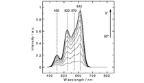
- FIG. 2 shows the angle dependence of the emission spectrum in S2 of Table 1
- FIG. 3 shows the angle dependence (maximum intensity normalization) of the emission spectrum in S2 of Table 1.
- FIG. 2 which is the sum of the light emitting dopants A, B, C, and D in this simulation, the average luminance / front luminance of 50 degrees to 70 degrees at each wavelength (450, 520, 570, 615) was confirmed. In 450, it was 1.16 at 520, 0.81 at 570, 0.97 at 570, and 0.81 at 615.
- Luminance average value of 50 ° -70 ° / front luminance (at emission peak wavelength of emission dopant A)> Brightness average value of 50 ° -70 ° / front luminance (at emission peak wavelength of emission dopant D)
- Brightness average value of 50 ° -70 ° / front luminance (at emission peak wavelength of emission dopant C)> Brightness average value of 50 ° -70 ° / front luminance (at emission peak wavelength of emission dopant B)
- the luminance average value of 50 ° -70 ° / front luminance must be 1.0, so in the spectrum which is certainly the sum of the four dopants, each luminescent dopant
- the angle dependency of the luminance at the wavelength is different from the angle dependency of one kind of dopant, the influence is not so strong that the magnitude relationship between the average luminance of 50 degrees-70 degrees / front luminance between the dopants is changed. This is because the angle dependence of the emission peak wavelength of each emission dopant is basically influenced by the emission dopant having the emission peak wavelength.
- T1, T2 and T3 indicate the angle dependency of the emission color when only the emission peak wavelength of the emission dopant B is changed among the emission dopants A, B, C, and D.
- coordinates in the u′v ′ color system corresponding to the peak wavelengths of the light-emitting dopants A, C, and D used in T1 are indicated by diamond marks.
- the coordinates in the u′v ′ color system corresponding to the wavelength 520 nm at T1 of the luminescent dopant B, the wavelength 500 nm at T2, and the wavelength 490 nm at T3 are indicated by circle marks.
- the coordinates in the u′v ′ color system corresponding to the peak wavelength are the coordinates of the spectrum of a sharp peak (standard deviation 1 nm) at the peak wavelength.
- the vector (vector DA) in FIG. ) Changes color.
- ⁇ in Table 2 is defined by the following equation [Expression 2], and the unit is degrees (however, the coordinates of A, B, C, and D are coordinates in the CIE color system).
- ⁇ in Table 2 is defined by the following formula [Equation 3], and the unit is degrees (however, the coordinates of A, B, C, and D are coordinates in the u′v ′ color system).
- ⁇ and ⁇ represent angles formed by the vector DA and the vector BC in the CIE color system and the u′v ′ color system, respectively.
- T1, T2, and T3 examined the viewing angle dependence of the luminescent color when the wavelength of the luminescent dopant B is 520, 500, and 490, respectively.
- the angles formed by the vector DA and the vector BC are smaller in the order of T1, T2, and T3 in both the CIE color system and the u′v ′ color system.
- the viewing angle dependence of the emission color also decreases in the order of T1, T2, and T3 in both the CIE color system and the u′v ′ color system.
- the viewing angle dependence of the CIE color system is also described.
- the viewing angle dependence of the u'v 'color system in which the distance of the color space is defined as an equal distance, is large or small. is important.
- U1 and U2 are compared.
- U1 and U2 change the wavelength of the luminescent dopant B among the luminescent dopants A, B, C, and D.
- the difference between T1, T2, T3 system is to have reversed magnitude relation of n B and n C.
- the emission color is more influenced by the luminescent dopant A than the luminescent dopant D as it goes from 0 degrees to 80 degrees. Becomes stronger.
- the vector (vector DA) in FIG. ) Changes color.
- the vector (vector DA) determined from the coordinates of the emission peak wavelength of the luminescent dopant D and the coordinates of the u'v 'color system corresponding to the emission peak wavelength of the emission dopant B and the light emission. It was shown that the vector (vector BC) determined from the coordinates of the u′v ′ color system corresponding to the emission peak wavelength of the dopant C is preferably substantially parallel.
- the combined vector of vector Y and vector Z is smaller than the combined vector of vector X and vector Z.
- the luminescent dopants are luminescent dopant A, luminescent dopant B, luminescent dopant C, and luminescent dopant D from the shorter wavelength, and the peak of luminescent dopant A in the u′v ′ color system.
- the coordinates corresponding to the wavelength are (x a , y a )
- the coordinates corresponding to the peak wavelength of the luminescent dopant B are (x b , y b )
- the coordinates corresponding to the peak wavelength of the luminescent dopant C are (x c , y c).
- the peak wavelength of the light-emitting dopant D becomes stronger as it becomes 0 to 80 degrees in the relationship between the light-emitting dopant A and the light-emitting dopant D.
- the vector Z is defined with the coordinates corresponding to the end point side and the coordinates corresponding to the weak emission dopant as the starting point side.
- a vector X represents a case where the light-emitting dopant B becomes strong at 0 to 80 degrees
- a vector Y represents a case where the light-emitting dopant C becomes strong.
- Vector X is (x b -x c, y b -y c)
- the vector Y is a (x c -x b, y c -y b).
- the vector Y is a case where the light emitting dopant C becomes strong at 0 to 80 degrees with respect to the light emitting dopant B and the light emitting dopant C.
- light-emitting dopants there are at least four types of light-emitting dopants, which are light-emitting dopant A, light-emitting dopant B, light-emitting dopant C, and light-emitting dopant D from the shorter wavelength, and u′v ′ table.
- a coordinate corresponding to the peak wavelength of the emission dopant a (x a, y a)
- the coordinate corresponding to the peak wavelength of the emission dopant B (x b, y b)
- corresponding to the peak wavelength of the emission dopant C (X c , y c )
- coordinates corresponding to the peak wavelength of the luminescent dopant D are (x d , y d )
- the relationship between the luminescent dopant A and the luminescent dopant D is 0 to 80 degrees.
- the vector Z is defined with the coordinates corresponding to the peak wavelength of the luminescent dopant becoming stronger as the end point side and the coordinates corresponding to the luminescent dopant becoming weaker as the start point side.
- the coordinates corresponding to the peak wavelength of the light-emitting dopant that becomes stronger from 0 degrees to 80 degrees are the end point side
- the coordinates corresponding to the weak light-emitting dopant are the start point side.
- the peak wavelengths of the light-emitting dopant B and the light-emitting dopant C exist on both sides with a boundary of 520 nm forming the outer edge vertex of the green region of the u′v ′ chromaticity diagram. That is, it is desirable that the peak wavelength of the luminescent dopant B ⁇ 520 nm and the peak wavelength of the luminescent dopant C> 520 nm.
- the peak wavelength of the luminescent dopant A is 450-470 nm
- the peak of the luminescent dopant B is It is particularly preferable that the wavelength is 495-510 nm, the peak wavelength of the luminescent dopant C is 540-580 nm, and the peak wavelength of the luminescent dopant D is 600-700 nm.
- various types of light emitting materials have been invented conventionally at each wavelength, and various kinds of light emitting materials have been conventionally invented. Is applicable.
- a particularly desirable form of the light-emitting dopant A is The peak wavelength is 450-470 nm, the peak wavelength of the luminescent dopant B is 495-510 nm, the peak wavelength of the luminescent dopant C is 540-580 nm, and the peak wavelength of the luminescent dopant D is 600-700 nm.
- Preferred examples of the light-emitting dopants A, B, C, and D of the present invention are listed below, but are not limited to the following examples, and any known material can be used.
- Green emission dopant as emission dopant C: Bt 2 Ir (acac): emission peak wavelength 570 nm, (peak wavelength u ′, v ′) (0.203, 0.570).
- TBP represents 1-tert-butyl-perylene.
- Bt 2 Ir (acac) represents bis (2-phenylbenzothiozolato-N—C2) iridium (III) acetylacetonate.
- Btp 2 Ir (acac) represents bis [2- (2′-benzothienyl) pyridinate-N, C3] iridium (III) acetylacetonate.
- Coumarin 6 represents 3- (2-benzothiazolyl) -7- (diethylamino) coumarin.
- singlet materials in the blue region include BCzVBi (4,4′-bis (9-ethyl-3-carbazovinylene) -1,1′-biphenyl), Perylene, TBPe (2, 5, 8 , 11-tetra-tert-butylperylene), BCzVB (9H-carbazole-3,3 ′-(1,4-phenylene-di-2,1-ethene-diyl) bis [9-ethyl- (9C)]) , DPAVBi (4,4-bis [4- (di-p-tolylamino) styryl] biphenyl).
- the triplet material in the blue region includes fac-Ir (Pmb) 3 (tris (1-phenyl-3-methylbenzimidazoline-2-ylidene-C, C2 ′), mer-Ir (Pmb) 3 (Tris ( 1-phenyl-3-methylbenzimidazoline-2-ylidene-C, C2 ′), etc.
- triplet material green-yellow region Ir (ppy) 3 (tris (2-phenylpyridine) iridium ( III)), Ir (ppy) 2 (acac) (bis (2-phenylpyridine) (acetylacetonato) iridium (III)), Ir (mppy) 3 (tris [2- (p-tolyl) pyridine] iridium ( III)) etc.
- Examples of singlet materials in the red region include DCM2 (4- (dicyanomethylene) -2-methyl-6-julolidyl-9-enyl-4H-pyran), DCJT (4 -(Dicyanomethylene) -2-methyl-6 (1,1,7,7-tetramethyljulolidyl-9-enyl) -4H-pyran) and the like.
- the triplet material of the region is Ir (btp) 2 (acac) (bis (2-benzo [b] thiophen-2-yl-pyridine) (acetylacetonato) iridium (III)), Ir (piq) 3
- examples thereof include (tris (1-phenylisoquinoline) iridium (III)), Ir (piq) 2 (acac) (bis (1-phenylisoquinoline) (acetylacetonato) iridium (III)) and the like.
- the light emitting dopant A is usually a blue light emitting material (peak wavelength of 500 nm or less), and the light emitting dopant D is a red light emitting material (peak wavelength). 600 nm or more).
- the light emitting dopants B and C are green or yellow light emitting materials (peak wavelength: 500 to 600 nm).
- the internal quantum efficiency of blue light-emitting materials is lower than the internal quantum efficiency of light-emitting materials of other colors, and the blue light-emitting material of triplet material has a short lifetime, so the lifetime is long, but the internal quantum efficiency is low.
- a blue light emitting material of a singlet material may be used, and the light emission intensity of the blue light emitting dopant in a state where no light scattering region is provided on the light extraction surface as described in Japanese Patent Application Laid-Open No. 2004-335183. Is weakened by interference in the front direction, and is strengthened in the oblique direction, and it is desirable to increase the blue light emitting dopant emission efficiency when the light scattering layer is formed.
- red light emitting layers usually tend to have higher luminous efficiency than other colors when other color light emitting layers are present. Therefore, when forming a highly efficient white light emitting organic electroluminescent element, red light emitting layer is used. The strength is often high. In this case, in the case where the light scattering layer is not formed, the red light emission when the light diffusion layer is formed is as follows: luminance average value of 50 ° -70 ° / front luminance (at the emission peak wavelength of the luminescent dopant D) ⁇ 1 It is desirable to reduce the gain of the luminous efficiency of the dopant.
- control of the interference of each light-emitting dopant is determined by controlling the distance between the light-emitting layer and the cathode, which is usually a reflective electrode.
- ⁇ is the emission wavelength of the light emitting layer in which the light emitting dopant of interest exists
- d is the distance between the light emitting layer and the cathode
- n is the refractive index of the layer existing between the light emitting layer and the cathode.
- optical interference design itself is not limited to the one described here, but may be designed using other well-known techniques. Basically, a technique of increasing or decreasing the luminance average value / front luminance of 50 to 70 degrees of a certain light emitting layer from 1 is a well-known technique.
- the interference control in the case where the cathode is a reflective electrode has been described. Even when the cathode is not a reflective electrode, whether each luminescent dopant is intensified in the front direction or intensified in the oblique direction with respect to Lambertian is related to optical interference. It can be generally predicted by numerical analysis, simulation, etc., and can be controlled by appropriately adjusting the hole transport layer thickness, the electron transport layer thickness, and the light emitting layer thickness.
- an organic EL layer is formed on a normal non-diffusible substrate, it is possible to easily check whether the element is suitable for the present invention, and by observing a cross section with a transmission electron microscope, If the thickness of each layer is known, the angular distribution of luminance can be predicted to some extent.
- the light emitting dopant A is a singlet light emitting material and the light emitting dopant D is a triplet light emitting material.
- the gain of improving the light emitting efficiency of the light emitting dopant A when the light scattering layer is provided is compared with the gain of improving the light emitting efficiency of the light emitting dopant D.
- the white light-emitting organic electroluminescence panel including a highly efficient white light-emitting organic electroluminescence element and a light scattering layer.
- the light emitting dopant C may be a triplet light emitting material. Since the light-emitting dopant A is a singlet material, a white organic electroluminescence device with high efficiency and long life can also be realized.
- the dopant A of the singlet light emitting material is the first light emitting unit
- the light emitting dopant D of the triplet light emitting material is the second light emitting unit. It is suitable for avoiding energy transfer.
- the light emitting dopant C is a triplet light emitting material
- the light emitting dopant C is preferably included in the second light emitting unit.
- the light-emitting dopant B is a singlet light-emitting material
- the light-emitting dopant B is preferably included in the second light-emitting unit if the light-emitting dopant B is a triplet light-emitting material.
- the cathode or the anode is a reflective electrode
- the first light emitting unit is more than the second light emitting unit. It is desirable to be at a position far from the reflective electrode. This is because the light extraction efficiency is usually higher in the range of 50 nm or more away from the reflective electrode, and the light emitting unit closer to the reflective electrode has a higher gain due to optical interference. When the gain due to optical interference is considered, the gain closer to the reflective electrode is higher because the order of interference as described in JP-A-2000-243573 is lower.
- the reflective electrode is a normal metal such as aluminum, and if the light emitting layer and the metal are too close, the exciton of the light emitting layer moves to the metal side, and extinction occurs for a reason other than optical interference.
- the distance between the light emitting layer and the cathode is preferably 30 nm or more. Since white light having a correlated color temperature of 2000-4500 K has a relatively high red light emission intensity, it is desirable that a red light emitting layer be present in the light emitting unit close to the reflective electrode.
Landscapes
- Physics & Mathematics (AREA)
- Optics & Photonics (AREA)
- Electroluminescent Light Sources (AREA)
Abstract
Description
この発明では、光拡散層を設ける前の状態において、特に、正面方向の発光は弱め合うが、素子内部に閉じ込められる導波光は強め合うような構成とされている。このように、通常は導波光として素子内部に閉じ込められる広角度成分の光を強め合うように基本構成を決定し、大部分の光量が分布する導波光を増幅した上で、上記光拡散層を形成すると、外部に出射できる正面方向の光が強め合うように基本構成を決定するよりも、発光効率が高められた有機エレクトロルミネッセンス素子が得られることが知られている。
尚、式(1)は下記式(2)とも言える。
また、特許文献2では複数色の発光層が存在する有機エレクトロルミネッセンス素子においては、効率の悪い色の発光層について陰極間と発光層の距離を最適化することが記されている。照明用途として有機エレクトロルミネッセンス素子を考えた場合、発光効率が高いだけでなく、発光色の視野角依存性も低減されることが望ましい。白色発光の有機エレクトロルミネッセンス素子として、発光色の視野角依存性がないことは理想的には各発光色の発光強度の視野角依存性がそろっていれば、発光色の視野角依存性がないことになるが、特許文献2のように光学干渉の効果を用いて各発光色の発光効率の調整を行う場合は、各発光色の発光強度の視野角依存性がそろっていないことを前提にしなければならない。
50度-70度の輝度平均値/正面輝度(発光ドーパントCの発光ピーク波長における)>50度-70度の輝度平均値/正面輝度(発光ドーパントBの発光ピーク波長における) …(F2)
これら式(F1)かつ式(F2)の条件を満たすことにより、高発光効率で低視野角依存性の白色発光有機エレクトロルミネッセンス素子を形成できるものである。
ここにおいて、前記「50度-70度の第一の輝度平均値」は、前記発光ドーパントAの発光ピーク波長における50度-70度の輝度平均値であり、前記「第一の正面輝度」は、前記発光ドーパントAの発光ピーク波長における正面輝度であり、前記「50度-70度の第二の輝度平均値」は、前記発光ドーパントDの発光ピーク波長における50度-70度の輝度平均値であり、前記「第二の正面輝度」は前記発光ドーパントDの発光ピーク波長における正面輝度である。
ここにおいて、前記「50度-70度の第三の輝度平均値」は、前記発光ドーパントCの発光ピーク波長における50度-70度の輝度平均値であり、前記「第三の正面輝度」は、前記発光ドーパントCの発光ピーク波長における正面輝度であり、前記「50度-70度の第四の輝度平均値」は、前記発光ドーパントBの発光ピーク波長における50度-70度の輝度平均値であり、前記「第四の正面輝度」は前記発光ドーパントBの発光ピーク波長における正面輝度である。
D(θ,n)=cosn(θ)で定義する。
n>1の場合、50-70度の放射輝度平均値<正面方向の放射輝度
n=1の場合、50-70度の放射輝度平均値=正面方向の放射輝度
n<1の場合、50-70度の放射輝度平均値>正面方向の放射輝度
となる。図1にn<1,n=1.0,n>1の場合の放射分布を示す。数値計算上
0<cos(θ)<1[0≦θ≦90°]であり、0<n1<n2である場合、
50-70度の放射輝度平均値/正面方向の放射輝度(n=n1)>50-70度の放射輝度平均値/正面方向の放射輝度(n=n2)が成立する。

PA,PB,PC,PDはそれぞれ、発光ドーパントA,B,C,Dの発光強度に比例する量である。D(θ,nA),DB(θ,nB),DC(θ,nC),DD(θ,nD)はそれぞれ、発光ドーパントA、B、C,Dの放射輝度の角度依存性を示す式である。λpA,λpB,λpC,λpDはそれぞれ発光ドーパントA、B、C、Dの発光ピーク波長(nm)である。σA、σB、σC、σDはそれぞれ発光ドーパントA、B、C、Dの発光スペクトルの標準偏差(nm)である。

50度-70度の輝度平均値/正面輝度(発光ドーパントAの発光ピーク波長における)>50度-70度の輝度平均値/正面輝度(発光ドーパントDの発光ピーク波長における)
が成立しており、
S1では、nB=1.0,nC=1.3なので、
50度-70度の輝度平均値/正面輝度(発光ドーパントCの発光ピーク波長における)<50度-70度の輝度平均値/正面輝度(発光ドーパントBの発光ピーク波長における)
であり、
S2では、nB=1.3,nC=1.0なので、
50度-70度の輝度平均値/正面輝度(発光ドーパントCの発光ピーク波長における)>50度-70度の輝度平均値/正面輝度(発光ドーパントBの発光ピーク波長における)
である。
50度-70度の輝度平均値/正面輝度(発光ドーパントAの発光ピーク波長における)<50度-70度の輝度平均値/正面輝度(発光ドーパントDの発光ピーク波長における)
が成立している。
50度-70度の輝度平均値/正面輝度(発光ドーパントCの発光ピーク波長における)>50度-70度の輝度平均値/正面輝度(発光ドーパントBの発光ピーク波長における)
である。
50度-70度の輝度平均値/正面輝度(発光ドーパントCの発光ピーク波長における)<50度-70度の輝度平均値/正面輝度(発光ドーパントBの発光ピーク波長における)
である。
50度-70度の輝度平均値/正面輝度(発光ドーパントAの発光ピーク波長における)>50度-70度の輝度平均値/正面輝度(発光ドーパントDの発光ピーク波長における)
において、
50度-70度の輝度平均値/正面輝度(発光ドーパントCの発光ピーク波長における)>50度-70度の輝度平均値/正面輝度(発光ドーパントBの発光ピーク波長における)
が、視野角依存性低減に有用な構成だと理解される。
50度-70度の輝度平均値/正面輝度(発光ドーパントAの発光ピーク波長における)と50度-70度の輝度平均値/正面輝度(発光ドーパントDの発光ピーク波長における)の大小関係および、
50度-70度の輝度平均値/正面輝度(発光ドーパントBの発光ピーク波長における)と50度-70度の輝度平均値/正面輝度(発光ドーパントCの発光ピーク波長における)の大小関係にわずかに影響があり、混ざっている状態においてはそれぞれの発光ドーパントピーク波長における角度依存性は、発光ドーパント単体の角度依存性と比べるとその他の発光ドーパントの角度依存性の影響をわずかに受けうる。しかし、それぞれの発光ドーパントのピークが最大ピークに対して約0.1倍以上あれば、混ざっている状態での各発光ピーク波長における不等号の向きは基本的に変わらないので、混ざっている状態でのそれぞれの発光ドーパントの発光ピーク波長における50度-70度の輝度平均値/正面輝度の大小の不等号の向きは、その発光ピーク波長をもつ発光ドーパントの50度-70度の輝度平均値/正面輝度の大小の不等号の向きと変わらない、と考えられる。
50度-70度の輝度平均値/正面輝度(発光ドーパントAの発光ピーク波長における)>50度-70度の輝度平均値/正面輝度(発光ドーパントDの発光ピーク波長における)
かつ、
50度-70度の輝度平均値/正面輝度(発光ドーパントCの発光ピーク波長における)>50度-70度の輝度平均値/正面輝度(発光ドーパントBの発光ピーク波長における)
を満たしている、といえる。
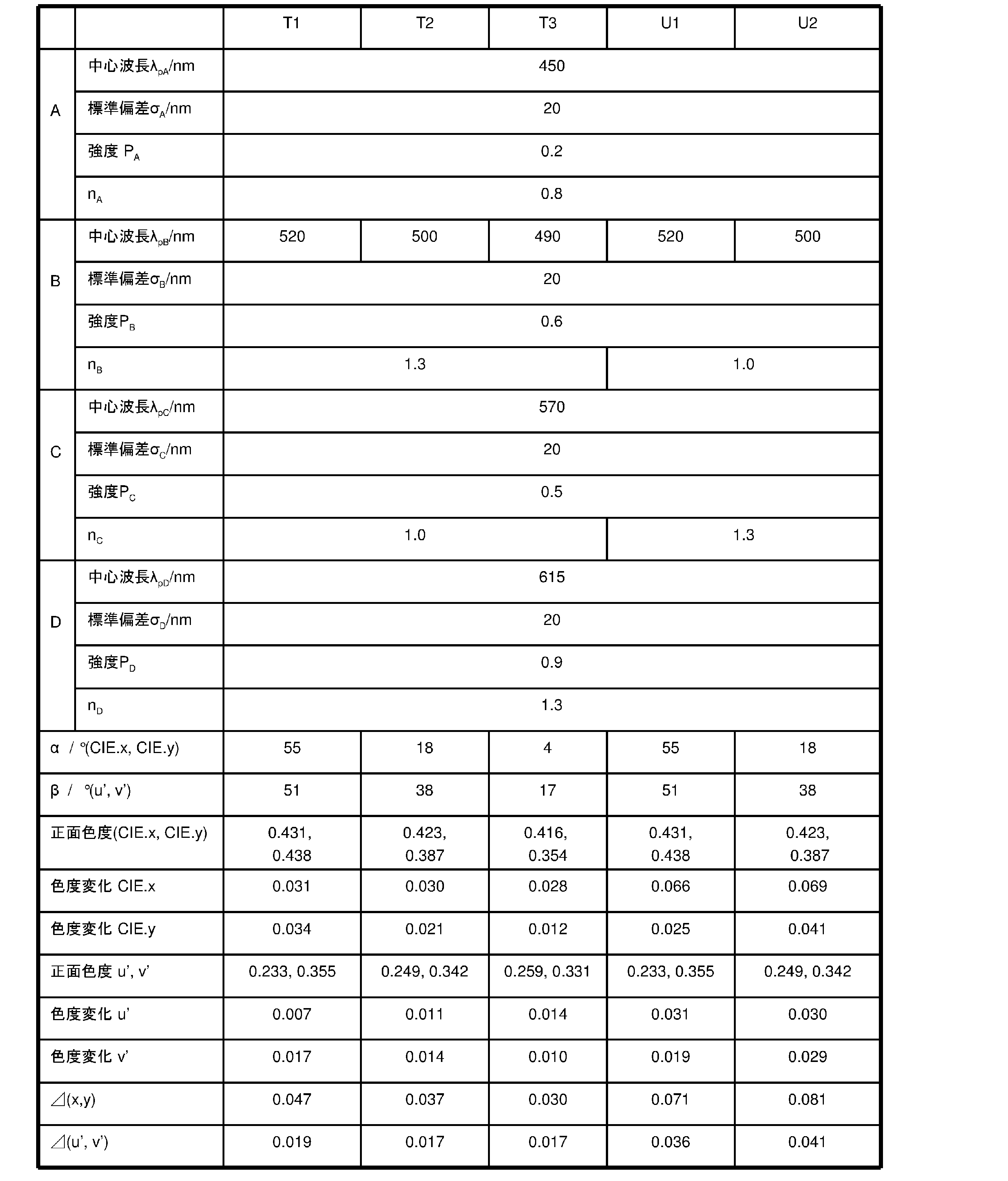

表2のβは次式[数3]で定義され、単位は度である(但し、A,B,C,Dの座標はu’v’表色系における座標である。)。

α、βはそれぞれ、CIE表色系、u’v’表色系におけるベクトルDAとベクトルBCの成す角度を示している。

より、ベクトルYとベクトルZの合成されたベクトルがベクトルXとベクトルZの合成されたベクトルよりも小さくなる。

となる。ベクトルYとは、発光ドーパントBと発光ドーパントCについて、0度から80度で発光ドーパントCが強くなる場合である。

とすると、斜め方向が強めあう。また、[数7]のように、

の場合、正面方向が強めあう。
P 白色発光有機エレクトロルミネッセンスパネル
1 発光ユニット
2 発光ユニット
3 中間接続層
10 陽極
11 陰極
12 光拡散層
Claims (12)
- 陽極と陰極の間に、発光ピーク波長の異なる少なくとも4種類の発光ドーパントを含む白色発光有機エレクトロルミネッセンス素子であって、
前記4種類の発光ドーパントは発光ピーク波長が発光ドーパントA、発光ドーパントB,発光ドーパントC,発光ドーパントDの順に長くなっており、
発光スペクトルが、
{50度-70度の第一の輝度平均値/第一の正面輝度}>{50度-70度の第二の輝度平均値/第二の正面輝度}であり、
ここにおいて、前記「50度-70度の第一の輝度平均値」は、前記発光ドーパントAの発光ピーク波長における50度-70度の輝度平均値であり、前記「第一の正面輝度」は、前記発光ドーパントAの発光ピーク波長における正面輝度であり、前記「50度-70度の第二の輝度平均値」は、前記発光ドーパントDの発光ピーク波長における50度-70度の輝度平均値であり、前記「第二の正面輝度」は前記発光ドーパントDの発光ピーク波長における正面輝度であり、
{50度-70度の第三の輝度平均値/第三の正面輝度}>{50度-70度の第四の輝度平均値/第四の正面輝度}であり、
ここにおいて、前記「50度-70度の第三の輝度平均値」は、前記発光ドーパントCの発光ピーク波長における50度-70度の輝度平均値であり、前記「第三の正面輝度」は、前記発光ドーパントCの発光ピーク波長における正面輝度であり、前記「50度-70度の第四の輝度平均値」は、前記発光ドーパントBの発光ピーク波長における50度-70度の輝度平均値であり、前記「第四の正面輝度」は前記発光ドーパントBの発光ピーク波長における正面輝度であることを特徴とする白色発光有機エレクトロルミネッセンス素子。 - 前記発光ドーパントBのピーク波長が480~520nmであり、前記発光ドーパントCのピーク波長が520~580nmであることを特徴とする請求項1に記載の白色発光有機エレクトロルミネッセンス素子。
- 前記発光ドーパントAは青色発光ドーパントであり、前記発光ドーパントDは赤色発光ドーパントであることを特徴する請求項1又は2に記載の白色発光有機エレクトロルミネッセンス素子。
- {50度-70度の第一の輝度平均値/第一の正面輝度}>1であることを特徴とする請求項1乃至3のいずれか1項に記載の白色発光有機エレクトロルミネッセンス素子。
- {50度-70度の第二の輝度平均値/第二の正面輝度}<1であることを特徴とする請求項1乃至4のいずれか1項に記載の白色発光有機エレクトロルミネッセンス素子。
- 前記陽極と前記陰極間に、2つの発光ユニットと、これら2つの発光ユニット間を接続する中間接続層とを設けてから構成され、前記一方の発光ユニットが前記発光ドーパントAを含み、前記他方の発光ユニットが前記発光ドーパントC及び前記発光ドーパントDを含むことを特徴とする請求項1乃至5のいずれか1項に記載の白色発光有機エレクトロルミネッセンス素子。
- 前記発光ドーパントAを含む前記一方の発光ユニットに前記発光ドーパントBが含有され、この発光ドーパントBは1重項発光材料であることを特徴とする請求項6に記載の白色発光有機エレクトロルミネッセンス素子。
- 前記発光ドーパントC及びDを含む前記他方の発光ユニットに前記発光ドーパントBが含有され、この発光ドーパントBは3重項発光材料であることを特徴とする請求項6に記載の白色発光有機エレクトロルミネッセンス素子。
- 前記発光ドーパントAは1重項発光材料であり、前記発光ドーパントC及びDは3重項発光材料であることを特徴とする請求項1乃至7のいずれか1項に記載の白色発光有機エレクトロルミネッセンス素子。
- 前記陽極と前記陰極のいずれか一方は反射性電極であり、前記一方の発光ユニットは前記他方の発光ユニットよりも前記反射性電極から遠い位置にあり、相関色温度2000-4500Kの白色発光を行うことを特徴とする請求項6乃至8のいずれか1項に記載の白色発光有機エレクトロルミネッセンス素子。
- 発光スペクトルが前記4種類の発光ドーパントからのみ由来していることを特徴とする請求項1乃至9のいずれか1項に記載の白色発光有機エレクトロルミネッセンス素子。
- 請求項1乃至10のいずれか1項に記載の白色発光有機エレクトロルミネッセンス素子の光取り出し面に散乱性の光拡散層が設けられていることを特徴とする白色発光有機エレクトロルミネッセンスパネル。
Priority Applications (4)
| Application Number | Priority Date | Filing Date | Title |
|---|---|---|---|
| JP2012543405A JP5238911B2 (ja) | 2011-03-24 | 2012-03-09 | 白色発光有機エレクトロルミネッセンス素子及び白色発光有機エレクトロルミネッセンスパネル |
| CN201280014972.5A CN103608943B (zh) | 2011-03-24 | 2012-03-09 | 白色发光有机电致发光元件和白色发光有机电致发光面板 |
| US14/006,447 US9184404B2 (en) | 2011-03-24 | 2012-03-09 | White light-emitting organic electroluminescent element and white light-emitting organic electroluminescent panel |
| DE112012001417T DE112012001417T5 (de) | 2011-03-24 | 2012-03-09 | Weißes Licht emittierendes organisches Elektrolumineszenzelement und weißes Licht emittierende organische Elektrolumineszenzplatte |
Applications Claiming Priority (2)
| Application Number | Priority Date | Filing Date | Title |
|---|---|---|---|
| JP2011-066567 | 2011-03-24 | ||
| JP2011066567 | 2011-03-24 |
Publications (1)
| Publication Number | Publication Date |
|---|---|
| WO2012128079A1 true WO2012128079A1 (ja) | 2012-09-27 |
Family
ID=46879233
Family Applications (1)
| Application Number | Title | Priority Date | Filing Date |
|---|---|---|---|
| PCT/JP2012/056134 Ceased WO2012128079A1 (ja) | 2011-03-24 | 2012-03-09 | 白色発光有機エレクトロルミネッセンス素子及び白色発光有機エレクトロルミネッセンスパネル |
Country Status (6)
| Country | Link |
|---|---|
| US (1) | US9184404B2 (ja) |
| JP (2) | JP5238911B2 (ja) |
| CN (1) | CN103608943B (ja) |
| DE (1) | DE112012001417T5 (ja) |
| TW (1) | TWI466353B (ja) |
| WO (1) | WO2012128079A1 (ja) |
Cited By (3)
| Publication number | Priority date | Publication date | Assignee | Title |
|---|---|---|---|---|
| WO2014010223A1 (ja) * | 2012-07-13 | 2014-01-16 | パナソニック株式会社 | 有機エレクトロルミネッセンス素子 |
| WO2014185063A1 (ja) * | 2013-05-17 | 2014-11-20 | パナソニックIpマネジメント株式会社 | 有機エレクトロルミネッセンス素子及び照明装置 |
| JP2016092256A (ja) * | 2014-11-06 | 2016-05-23 | コニカミノルタ株式会社 | 面発光モジュール |
Families Citing this family (6)
| Publication number | Priority date | Publication date | Assignee | Title |
|---|---|---|---|---|
| US9379359B2 (en) | 2013-03-13 | 2016-06-28 | Panasonic Intellectual Property Management Co., Ltd. | Organic electroluminescence element and lighting device using same |
| CN105027671B (zh) | 2013-04-12 | 2017-09-22 | 松下知识产权经营株式会社 | 发光装置 |
| US9179511B2 (en) | 2013-07-08 | 2015-11-03 | Panasonic Intellectual Property Management Co., Ltd. | Light-emitting device, and light source for lighting and lighting apparatus using the same |
| WO2016076187A1 (ja) * | 2014-11-14 | 2016-05-19 | コニカミノルタ株式会社 | 有機エレクトロルミネッセンス素子 |
| JPWO2016088513A1 (ja) * | 2014-12-04 | 2017-09-14 | コニカミノルタ株式会社 | 有機エレクトロルミネッセンス素子 |
| JP2016225221A (ja) * | 2015-06-02 | 2016-12-28 | コニカミノルタ株式会社 | 電界発光素子 |
Citations (5)
| Publication number | Priority date | Publication date | Assignee | Title |
|---|---|---|---|---|
| JP2004296423A (ja) * | 2002-11-26 | 2004-10-21 | Nitto Denko Corp | 有機エレクトロルミネッセンス素子、面光源および表示装置 |
| JP2010539653A (ja) * | 2007-09-17 | 2010-12-16 | グローバル オーエルイーディー テクノロジー リミティド ライアビリティ カンパニー | 向上した光出力を有するledデバイス |
| JP2010287524A (ja) * | 2009-06-15 | 2010-12-24 | Sony Corp | 表示素子および表示装置 |
| JP2010541160A (ja) * | 2007-09-28 | 2010-12-24 | グローバル オーエルイーディー テクノロジー リミティド ライアビリティ カンパニー | 光出力を改良したledデバイス |
| JP2011049356A (ja) * | 2009-08-27 | 2011-03-10 | Nippon Seiki Co Ltd | 有機el素子 |
Family Cites Families (19)
| Publication number | Priority date | Publication date | Assignee | Title |
|---|---|---|---|---|
| JPH03272860A (ja) | 1990-03-22 | 1991-12-04 | Canon Inc | インクジェット記録装置のインク吸引回復装置 |
| JPH06240227A (ja) | 1993-02-19 | 1994-08-30 | Mitsui Toatsu Chem Inc | 一液湿気硬化型ウレタン接着剤 |
| JP2846571B2 (ja) | 1994-02-25 | 1999-01-13 | 出光興産株式会社 | 有機エレクトロルミネッセンス素子 |
| JP3272860B2 (ja) | 1994-03-03 | 2002-04-08 | エヌオーケー株式会社 | 中空糸膜モジュール及びその製造方法 |
| JP3884564B2 (ja) | 1998-05-20 | 2007-02-21 | 出光興産株式会社 | 有機el発光素子およびそれを用いた発光装置 |
| JP4001692B2 (ja) | 1999-02-18 | 2007-10-31 | パイオニア株式会社 | 有機エレクトロルミネッセンス素子とその製造方法 |
| US6431174B1 (en) * | 2000-08-10 | 2002-08-13 | Pi Medical, Inc. | Method and apparatus to treat conditions of the naso-pharyngeal area |
| US6506901B2 (en) | 2000-07-17 | 2003-01-14 | Wyeth | Substituted 2-(S)-hydroxy-3-(piperidin-4-yl-methylamino)-propyl ethers and substituted 2-aryl-2-(R)-hydroxy-1-(piperidin-4-yl-methyl)-ethylamine β-3 adrenergic receptor agonists |
| JP3933591B2 (ja) | 2002-03-26 | 2007-06-20 | 淳二 城戸 | 有機エレクトロルミネッセント素子 |
| US6717358B1 (en) | 2002-10-09 | 2004-04-06 | Eastman Kodak Company | Cascaded organic electroluminescent devices with improved voltage stability |
| JP2004335181A (ja) | 2003-05-01 | 2004-11-25 | Japan Storage Battery Co Ltd | 非水電解質二次電池の放電方法 |
| JP4393788B2 (ja) | 2003-05-01 | 2010-01-06 | 日東電工株式会社 | エレクトロルミネッセンス素子、面光源および表示装置 |
| CN1961613B (zh) | 2004-03-26 | 2011-06-29 | 松下电工株式会社 | 有机发光器件 |
| KR101215279B1 (ko) * | 2004-05-21 | 2012-12-26 | 가부시키가이샤 한도오따이 에네루기 켄큐쇼 | 조명 장치 |
| EP2271183B1 (en) * | 2004-07-23 | 2015-03-18 | Konica Minolta Holdings, Inc. | Organic electroluminescent element, display and illuminator |
| JP4315874B2 (ja) | 2004-07-30 | 2009-08-19 | 三洋電機株式会社 | 有機エレクトロルミネッセント素子及び有機エレクトロルミネッセント表示装置 |
| JP4626967B2 (ja) | 2004-12-07 | 2011-02-09 | スタンレー電気株式会社 | 面発光素子及びその製造方法 |
| DE502005002342D1 (de) * | 2005-03-15 | 2008-02-07 | Novaled Ag | Lichtemittierendes Bauelement |
| KR101750301B1 (ko) | 2009-05-29 | 2017-06-23 | 가부시키가이샤 한도오따이 에네루기 켄큐쇼 | 발광 소자, 발광 장치, 전자기기 및 조명 장치 |
-
2012
- 2012-03-09 WO PCT/JP2012/056134 patent/WO2012128079A1/ja not_active Ceased
- 2012-03-09 US US14/006,447 patent/US9184404B2/en active Active
- 2012-03-09 CN CN201280014972.5A patent/CN103608943B/zh active Active
- 2012-03-09 JP JP2012543405A patent/JP5238911B2/ja active Active
- 2012-03-09 DE DE112012001417T patent/DE112012001417T5/de not_active Ceased
- 2012-03-09 TW TW101108170A patent/TWI466353B/zh not_active IP Right Cessation
-
2013
- 2013-03-29 JP JP2013074213A patent/JP2013153198A/ja active Pending
Patent Citations (5)
| Publication number | Priority date | Publication date | Assignee | Title |
|---|---|---|---|---|
| JP2004296423A (ja) * | 2002-11-26 | 2004-10-21 | Nitto Denko Corp | 有機エレクトロルミネッセンス素子、面光源および表示装置 |
| JP2010539653A (ja) * | 2007-09-17 | 2010-12-16 | グローバル オーエルイーディー テクノロジー リミティド ライアビリティ カンパニー | 向上した光出力を有するledデバイス |
| JP2010541160A (ja) * | 2007-09-28 | 2010-12-24 | グローバル オーエルイーディー テクノロジー リミティド ライアビリティ カンパニー | 光出力を改良したledデバイス |
| JP2010287524A (ja) * | 2009-06-15 | 2010-12-24 | Sony Corp | 表示素子および表示装置 |
| JP2011049356A (ja) * | 2009-08-27 | 2011-03-10 | Nippon Seiki Co Ltd | 有機el素子 |
Cited By (6)
| Publication number | Priority date | Publication date | Assignee | Title |
|---|---|---|---|---|
| WO2014010223A1 (ja) * | 2012-07-13 | 2014-01-16 | パナソニック株式会社 | 有機エレクトロルミネッセンス素子 |
| US9431624B2 (en) | 2012-07-13 | 2016-08-30 | Panasonic Intellectual Property Management Co., Ltd. | Organic electroluminescent element |
| WO2014185063A1 (ja) * | 2013-05-17 | 2014-11-20 | パナソニックIpマネジメント株式会社 | 有機エレクトロルミネッセンス素子及び照明装置 |
| JPWO2014185063A1 (ja) * | 2013-05-17 | 2017-02-23 | パナソニックIpマネジメント株式会社 | 有機エレクトロルミネッセンス素子及び照明装置 |
| US9786859B2 (en) | 2013-05-17 | 2017-10-10 | Panasonic Intellectual Property Management Co., Ltd. | Organic electroluminescent element and lighting device |
| JP2016092256A (ja) * | 2014-11-06 | 2016-05-23 | コニカミノルタ株式会社 | 面発光モジュール |
Also Published As
| Publication number | Publication date |
|---|---|
| TWI466353B (zh) | 2014-12-21 |
| DE112012001417T5 (de) | 2013-12-24 |
| US20140008632A1 (en) | 2014-01-09 |
| CN103608943A (zh) | 2014-02-26 |
| JP5238911B2 (ja) | 2013-07-17 |
| CN103608943B (zh) | 2016-02-10 |
| TW201244209A (en) | 2012-11-01 |
| JP2013153198A (ja) | 2013-08-08 |
| JPWO2012128079A1 (ja) | 2014-07-24 |
| US9184404B2 (en) | 2015-11-10 |
Similar Documents
| Publication | Publication Date | Title |
|---|---|---|
| JP5238911B2 (ja) | 白色発光有機エレクトロルミネッセンス素子及び白色発光有機エレクトロルミネッセンスパネル | |
| US20200287153A1 (en) | Single-doped white oleds with extraction layer doped with down-conversion red emitters | |
| KR101451099B1 (ko) | 유기 일렉트로루미네슨스 소자, 및 이 소자를 각각 사용한 발광장치, 화상형성장치, 발광소자 어레이, 표시장치 및 촬상장치 | |
| US20140183496A1 (en) | Organic light emitting display device and method of manufacturing the same | |
| US9666644B2 (en) | Organic electroluminescent element | |
| KR20140079166A (ko) | 유기 발광 표시 장치 | |
| US12557533B2 (en) | Display panel and display device thereof | |
| KR20140086803A (ko) | 유기 발광 표시 장치 및 그 제조 방법 | |
| US20060192471A1 (en) | Organic electroluminescent device | |
| WO2017043245A1 (ja) | 有機エレクトロルミネッセンス装置、有機エレクトロルミネッセンス装置の製造方法、照明装置、および表示装置 | |
| WO2019105160A1 (zh) | 有机发光显示装置 | |
| JP2007234253A (ja) | 有機エレクトロルミネッセンス素子 | |
| US10879483B2 (en) | Organic electroluminescent device and illumination device | |
| JP2006244713A (ja) | 有機エレクトロルミネッセント素子 | |
| Zhai et al. | Enhanced light extraction from green organic light-emitting diodes by attaching a high-haze random-bowls textured optical film | |
| Arneson et al. | Color‐Stable, All‐Phosphorescent White Organic Light Emitting Diodes Using the Polariton‐Enhanced Purcell Effect | |
| Dong et al. | Eliminate angular color shift in top‐emitting OLEDs through cavity design | |
| JP2005310746A (ja) | 発光表示装置 | |
| Chen et al. | Alleviate microcavity effects in top-emitting white organic light-emitting diodes for achieving broadband and high color rendition emission spectra | |
| CN105304683B (zh) | Oled显示器及其显示模组 | |
| Sharma et al. | Efficiency improvement of organic light-emitting diodes device by attaching microlens arrays and dependencies on the aspect ratio: A Sharma et al. | |
| Cho et al. | Strategic use of dopants and device structure optimization for enhanced color gamut and efficiency in organic light-emitting diodes microdisplay applications | |
| Li et al. | High-performance narrow spectrum green phosphorescent top-emitting organic light-emitting devices with external quantum efficiency up to 38% | |
| Tan et al. | 33‐3: Systematic Optimization for Achieving Indistinguishable Color Shift of RGB OLED Displays | |
| Tsuboi et al. | Recombination zone in white organic light emitting diodes with blue and orange emitting layers |
Legal Events
| Date | Code | Title | Description |
|---|---|---|---|
| ENP | Entry into the national phase |
Ref document number: 2012543405 Country of ref document: JP Kind code of ref document: A |
|
| 121 | Ep: the epo has been informed by wipo that ep was designated in this application |
Ref document number: 12761430 Country of ref document: EP Kind code of ref document: A1 |
|
| WWE | Wipo information: entry into national phase |
Ref document number: 14006447 Country of ref document: US |
|
| WWE | Wipo information: entry into national phase |
Ref document number: 1120120014170 Country of ref document: DE Ref document number: 112012001417 Country of ref document: DE |
|
| 122 | Ep: pct application non-entry in european phase |
Ref document number: 12761430 Country of ref document: EP Kind code of ref document: A1 |