WO2012128084A1 - Substrat de réseau de transistors à couches minces et dispositif d'affichage à cristaux liquides - Google Patents
Substrat de réseau de transistors à couches minces et dispositif d'affichage à cristaux liquides Download PDFInfo
- Publication number
- WO2012128084A1 WO2012128084A1 PCT/JP2012/056170 JP2012056170W WO2012128084A1 WO 2012128084 A1 WO2012128084 A1 WO 2012128084A1 JP 2012056170 W JP2012056170 W JP 2012056170W WO 2012128084 A1 WO2012128084 A1 WO 2012128084A1
- Authority
- WO
- WIPO (PCT)
- Prior art keywords
- electrode
- liquid crystal
- crystal display
- electrodes
- substrate
- Prior art date
- Legal status (The legal status is an assumption and is not a legal conclusion. Google has not performed a legal analysis and makes no representation as to the accuracy of the status listed.)
- Ceased
Links
Images

































Classifications
-
- G—PHYSICS
- G02—OPTICS
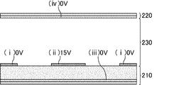
- G02F—OPTICAL DEVICES OR ARRANGEMENTS FOR THE CONTROL OF LIGHT BY MODIFICATION OF THE OPTICAL PROPERTIES OF THE MEDIA OF THE ELEMENTS INVOLVED THEREIN; NON-LINEAR OPTICS; FREQUENCY-CHANGING OF LIGHT; OPTICAL LOGIC ELEMENTS; OPTICAL ANALOGUE/DIGITAL CONVERTERS
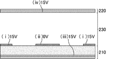
- G02F1/00—Devices or arrangements for the control of the intensity, colour, phase, polarisation or direction of light arriving from an independent light source, e.g. switching, gating or modulating; Non-linear optics
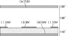
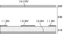
- G02F1/01—Devices or arrangements for the control of the intensity, colour, phase, polarisation or direction of light arriving from an independent light source, e.g. switching, gating or modulating; Non-linear optics for the control of the intensity, phase, polarisation or colour
- G02F1/13—Devices or arrangements for the control of the intensity, colour, phase, polarisation or direction of light arriving from an independent light source, e.g. switching, gating or modulating; Non-linear optics for the control of the intensity, phase, polarisation or colour based on liquid crystals, e.g. single liquid crystal display cells
- G02F1/133—Constructional arrangements; Operation of liquid crystal cells; Circuit arrangements
- G02F1/1333—Constructional arrangements; Manufacturing methods
- G02F1/1343—Electrodes
- G02F1/134309—Electrodes characterised by their geometrical arrangement
- G02F1/134363—Electrodes characterised by their geometrical arrangement for applying an electric field parallel to the substrate, i.e. in-plane switching [IPS]
-
- H—ELECTRICITY
- H10—SEMICONDUCTOR DEVICES; ELECTRIC SOLID-STATE DEVICES NOT OTHERWISE PROVIDED FOR
- H10D—INORGANIC ELECTRIC SEMICONDUCTOR DEVICES
- H10D30/00—Field-effect transistors [FET]
- H10D30/60—Insulated-gate field-effect transistors [IGFET]
- H10D30/67—Thin-film transistors [TFT]
- H10D30/674—Thin-film transistors [TFT] characterised by the active materials
- H10D30/6755—Oxide semiconductors, e.g. zinc oxide, copper aluminium oxide or cadmium stannate
-
- G—PHYSICS
- G02—OPTICS
- G02F—OPTICAL DEVICES OR ARRANGEMENTS FOR THE CONTROL OF LIGHT BY MODIFICATION OF THE OPTICAL PROPERTIES OF THE MEDIA OF THE ELEMENTS INVOLVED THEREIN; NON-LINEAR OPTICS; FREQUENCY-CHANGING OF LIGHT; OPTICAL LOGIC ELEMENTS; OPTICAL ANALOGUE/DIGITAL CONVERTERS
- G02F1/00—Devices or arrangements for the control of the intensity, colour, phase, polarisation or direction of light arriving from an independent light source, e.g. switching, gating or modulating; Non-linear optics
- G02F1/01—Devices or arrangements for the control of the intensity, colour, phase, polarisation or direction of light arriving from an independent light source, e.g. switching, gating or modulating; Non-linear optics for the control of the intensity, phase, polarisation or colour
- G02F1/13—Devices or arrangements for the control of the intensity, colour, phase, polarisation or direction of light arriving from an independent light source, e.g. switching, gating or modulating; Non-linear optics for the control of the intensity, phase, polarisation or colour based on liquid crystals, e.g. single liquid crystal display cells
- G02F1/133—Constructional arrangements; Operation of liquid crystal cells; Circuit arrangements
- G02F1/136—Liquid crystal cells structurally associated with a semi-conducting layer or substrate, e.g. cells forming part of an integrated circuit
- G02F1/1362—Active matrix addressed cells
- G02F1/1368—Active matrix addressed cells in which the switching element is a three-electrode device
-
- G—PHYSICS
- G02—OPTICS
- G02F—OPTICAL DEVICES OR ARRANGEMENTS FOR THE CONTROL OF LIGHT BY MODIFICATION OF THE OPTICAL PROPERTIES OF THE MEDIA OF THE ELEMENTS INVOLVED THEREIN; NON-LINEAR OPTICS; FREQUENCY-CHANGING OF LIGHT; OPTICAL LOGIC ELEMENTS; OPTICAL ANALOGUE/DIGITAL CONVERTERS
- G02F1/00—Devices or arrangements for the control of the intensity, colour, phase, polarisation or direction of light arriving from an independent light source, e.g. switching, gating or modulating; Non-linear optics
- G02F1/01—Devices or arrangements for the control of the intensity, colour, phase, polarisation or direction of light arriving from an independent light source, e.g. switching, gating or modulating; Non-linear optics for the control of the intensity, phase, polarisation or colour
- G02F1/13—Devices or arrangements for the control of the intensity, colour, phase, polarisation or direction of light arriving from an independent light source, e.g. switching, gating or modulating; Non-linear optics for the control of the intensity, phase, polarisation or colour based on liquid crystals, e.g. single liquid crystal display cells
- G02F1/133—Constructional arrangements; Operation of liquid crystal cells; Circuit arrangements
- G02F1/1333—Constructional arrangements; Manufacturing methods
- G02F1/1343—Electrodes
- G02F1/134309—Electrodes characterised by their geometrical arrangement
- G02F1/134381—Hybrid switching mode, i.e. for applying an electric field with components parallel and orthogonal to the substrates
Definitions
- the present invention relates to a thin film transistor array substrate and a liquid crystal display device. More specifically, the present invention relates to a liquid crystal display device including liquid crystal molecules that are aligned in a direction perpendicular to the main surface of the substrate when no voltage is applied, and a thin film transistor array substrate used in the liquid crystal display device.
- a liquid crystal display panel is configured by sandwiching a liquid crystal display element between a pair of glass substrates and the like, taking advantage of its thin, lightweight, and low power consumption characteristics, such as personal computers, televisions, car navigation systems, and other portable devices.
- the display of a portable information terminal such as a telephone is indispensable for daily life and business.
- liquid crystal display panels of various modes related to electrode arrangement and substrate design for changing the optical characteristics of the liquid crystal layer have been studied.
- VA vertical alignment
- IPS In-plane switching
- FFS fringe field switching
- an FFS driving type liquid crystal display device a thin film transistor type liquid crystal display having high-speed response and a wide viewing angle, a first substrate having a first common electrode layer, a pixel electrode layer, and a second common A second substrate having both electrode layers, a liquid crystal sandwiched between the first substrate and the second substrate, high-speed response to a high input data transfer rate, and a wide field of view for a viewer An electric field is generated between the first common electrode layer on the first substrate and both the pixel electrode layer and the second common electrode layer on the second substrate to provide a corner.
- a display including the means is disclosed (for example, refer to Patent Document 1).
- a liquid crystal device for applying a lateral electric field by a plurality of electrodes a liquid crystal device in which a liquid crystal layer made of a liquid crystal having a positive dielectric anisotropy is sandwiched between a pair of substrates arranged opposite to each other, The first substrate and the second substrate constituting the substrate are opposed to each other with the liquid crystal layer sandwiched therebetween, and an electrode for applying a vertical electric field to the liquid crystal layer is provided.
- a liquid crystal device provided with a plurality of electrodes for applying a lateral electric field to the liquid crystal layer is disclosed (for example, see Patent Document 2).
- the rise occurs between the upper layer slit electrode and the lower surface electrode on the lower substrate.
- the fringe electric field Due to the fringe electric field (FFS drive), the fall (while the display state changes from the bright state [white display] to the dark state [black display]) is caused by the vertical electric field generated by the potential difference between the substrates. It can be rotated for high speed response.
- FFS drive fringe electric field
- Patent Document 1 even when a fringe electric field is applied to a liquid crystal display device in which liquid crystal molecules are vertically aligned using a slit electrode, only the liquid crystal molecules near the end of the slit electrode rotate (see FIG. 66), sufficient transmittance cannot be obtained.
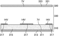
- FIG. 64 is a schematic cross-sectional view of a liquid crystal display panel having a conventional FFS drive type electrode structure on the lower substrate.
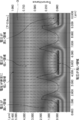
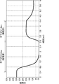
- FIG. 66 shows simulation results showing the distribution of the director D, the electric field distribution, and the transmittance distribution in the liquid crystal display panel shown in FIG. 64 shows the structure of the liquid crystal display panel, in which the slit electrode is applied to a constant voltage (in the figure, 14 V.
- the potential difference with the counter electrode 313 may be equal to or greater than a threshold value.
- Counter electrodes 313 and 323 are arranged. The counter electrodes 313 and 323 are 7V.
- FIG. 66 shows the simulation result at the rising edge, and shows the voltage distribution, the distribution of the director D, and the transmittance distribution
- Patent Document 2 describes that a response speed is improved by using comb driving in a liquid crystal display device having a three-layer electrode structure.
- a response speed is improved by using comb driving in a liquid crystal display device having a three-layer electrode structure.
- a twisted nematic (TN) mode liquid crystal device as a display method, and a vertical alignment type liquid crystal display device that is advantageous for obtaining a wide viewing angle, high contrast characteristics, etc.
- TN twisted nematic
- the present invention has been made in view of the above situation, and in a liquid crystal display device including a liquid crystal molecule in which a liquid crystal layer is aligned in a direction perpendicular to a main surface of a substrate when no voltage is applied, a sufficiently high-speed response is achieved.
- An object of the present invention is to provide a liquid crystal display device having sufficiently high transmittance.
- Another object of the present invention is to provide a thin film transistor array substrate suitably used for these liquid crystal display devices.
- the inventors of the present invention have studied to achieve both high-speed response and high transmittance in a vertical alignment type liquid crystal display device, and achieved a three-layer electrode structure in which alignment of liquid crystal molecules is controlled by an electric field at both rising and falling. Pay attention. Further investigation is made on the electrode structure, and the first substrate and the second substrate sandwiching the liquid crystal layer have electrodes, and the electrodes on the second substrate are used as a pair of comb-teeth electrodes. It has been found that a horizontal electric field is generated by the potential difference between the tooth electrodes, and a vertical electric field is generated by the potential difference between the substrates, so that switching of the vertical electric field ON to the horizontal electric field ON by the three-layer electrode structure can be suitably performed.
- the liquid crystal molecules can be rotated by an electric field for both rising and falling to achieve high-speed response, and a high transmittance can be realized by a lateral electric field driven by a comb tooth, and the above problem can be solved brilliantly.
- the present invention has been achieved.
- the liquid crystal display device having the vertical alignment type three-layer electrode structure as described above it is possible to realize high-speed response and high transmittance, and in this respect, the invention described in the prior art document Different. Furthermore, the problem of response speed becomes particularly noticeable in a low-temperature environment. In the present invention, this problem can be solved and the transmittance can be improved.
- the invention related to the present invention is a liquid crystal display panel comprising a first substrate, a second substrate, and a liquid crystal layer sandwiched between both substrates, wherein the first substrate and the second substrate have electrodes.
- the electrode of the second substrate includes a pair of comb electrodes and a planar electrode, and the liquid crystal display panel is generated between the pair of comb electrodes or between the first substrate and the second substrate.
- the liquid crystal display panel is configured such that liquid crystal molecules in a liquid crystal layer are aligned in a horizontal direction with respect to a main surface of a substrate by an electric field.
- the planar electrode is usually formed through a pair of comb electrodes and an electric resistance layer.
- the electrical resistance layer is preferably an insulating layer.
- the insulating layer may be an insulating layer in the technical field of the present invention.
- the pair of comb electrodes may be anything as long as it can be said that the two comb electrodes face each other when the substrate main surface is viewed in plan. Since a pair of comb electrodes can generate a lateral electric field between the comb electrodes, when the liquid crystal layer includes liquid crystal molecules having positive dielectric anisotropy, the response performance and transmission at the time of rising When the liquid crystal layer includes liquid crystal molecules having negative dielectric anisotropy, the liquid crystal molecules can be rotated by a lateral electric field at the time of falling to achieve a high-speed response.
- the electrodes of the first substrate and the second substrate may be any electrode as long as it can provide a potential difference between the substrates, whereby the liquid crystal layer has liquid crystal molecules having positive dielectric anisotropy.
- a vertical electric field is generated by the potential difference between the substrates at the time of falling when including and when the liquid crystal layer includes liquid crystal molecules having negative dielectric anisotropy, and the liquid crystal molecules are rotated by the electric field and rotated at high speed. Can be responsive.
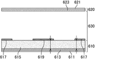
- 71 and 72 are cross-sectional schematic views showing one embodiment of the comb electrode of the liquid crystal display panel according to the present invention.
- a pair of comb electrodes 417, 419 may be provided in the same layer, and as shown in FIG. 72, as long as the effects of the present invention can be exhibited, a pair of comb electrodes is provided.
- the tooth electrodes 517 and 519 may be provided in different layers, but the pair of comb electrodes are preferably provided in the same layer.
- a pair of comb electrodes is provided in the same layer when each comb electrode has a common member (for example, an insulating layer, a liquid crystal layer side and / or a side opposite to the liquid crystal layer side). A liquid crystal layer, etc.).
- the comb-tooth portions are respectively along when the main surface of the substrate is viewed in plan.
- the comb-tooth portions of the pair of comb-tooth electrodes are substantially parallel, in other words, each of the pair of comb-tooth electrodes has a plurality of substantially parallel slits.
- the comb-tooth electrode which has one comb-tooth part typically is shown by FIG. 19 etc., normally one comb-tooth electrode has two or more comb-tooth parts.
- the liquid crystal layer preferably includes liquid crystal molecules that are aligned in a direction perpendicular to the main surface of the substrate when no voltage is applied.
- the term “orienting in the direction perpendicular to the main surface of the substrate” may be anything that can be said to be oriented in the direction perpendicular to the main surface of the substrate. Including. It is preferable that the liquid crystal molecules contained in the liquid crystal layer are substantially composed of liquid crystal molecules that are aligned in a direction perpendicular to the main surface of the substrate at a voltage lower than the threshold voltage.
- the “when no voltage is applied” may be anything as long as it can be said that substantially no voltage is applied in the technical field of the present invention.
- Such a vertical alignment type liquid crystal display panel is an advantageous system for obtaining a wide viewing angle, high contrast characteristics, and the like, and its application is expanding.
- the pair of comb electrodes can have different potentials at a threshold voltage or higher.
- it means a voltage value that gives a transmittance of 5% when the transmittance in the bright state is set to 100%.
- the potential different from the threshold voltage can be any voltage as long as it can realize a driving operation with a potential different from the threshold voltage. This makes it possible to suitably control the electric field applied to the liquid crystal layer. Become.
- a preferable upper limit value of the different potential is, for example, 20V.
- one of the pair of comb electrodes is driven by one TFT and the other comb electrode is driven by another TFT.
- a pair of comb electrodes can be set to different potentials by conducting with the lower electrode of the other comb electrode.
- the width of the comb tooth portion in the pair of comb electrodes is preferably 2 ⁇ m or more, for example.
- the width between the comb tooth portions (also referred to as a space in the present specification) is preferably 2 ⁇ m to 7 ⁇ m, for example.
- the liquid crystal display panel is configured such that liquid crystal molecules in a liquid crystal layer are aligned in a direction perpendicular to the main surface of the substrate by an electric field generated between a pair of comb electrodes or between a first substrate and a second substrate.
- the electrode of the first substrate is preferably a planar electrode.
- the planar electrode includes a form electrically connected within a plurality of pixels, for example, as a planar electrode of the first substrate, a form electrically connected within all pixels, A configuration in which the electrodes are electrically connected along the pixel line is preferable.
- the second substrate preferably further includes a planar electrode. Thereby, a vertical electric field can be applied suitably and high-speed response can be achieved.
- the electrode of the first substrate is a planar electrode and the second substrate further has a planar electrode
- a vertical electric field can be suitably generated by a potential difference between the substrates at the time of falling. Can be made to respond quickly.
- the liquid crystal layer side electrode (upper layer electrode) of the second substrate is used as a pair of comb-teeth electrodes, and the electrode on the opposite side of the second substrate from the liquid crystal layer side (lower layer)
- a form in which the electrode is a planar electrode is particularly preferable.
- the planar electrode of the second substrate can be provided below the pair of comb electrodes on the second substrate (the layer on the side opposite to the liquid crystal layer as viewed from the second substrate) via an insulating layer.
- the planar electrodes of the second substrate are preferably electrically connected along pixel lines, but may be independent for each pixel.
- the comb-shaped electrode is electrically connected to the lower-layer planar electrode and the planar electrode is electrically connected along the pixel line, the comb-shaped electrode also follows the pixel line.
- this form is also one of the preferred forms of the present invention.
- substrate is planar at least the location which overlaps with the electrode which a 1st board
- the term “electrically connected along the pixel line” may be used as long as it is electrically connected across a plurality of pixels along at least one of the vertical and horizontal arrays of pixels.
- the electrodes it is not necessary for the electrodes to be electrically connected to all the pixel lines, and any electrode can be used as long as it can be said to be substantially electrically connected along the pixel lines in the liquid crystal display panel.
- the electrode being electrically connected along the pixel line may be an electrode in which the electrodes in the picture element of one pixel line are electrically connected, It can be said that the electrodes in the picture elements of the pixel line in the plurality of pixel lines are electrically connected in order between the pixel lines, and the entire electrically connected electrodes are along the pixel line. It may be.
- the electrodes in the picture element of the pixel line in the plurality of pixel lines are electrically connected in order between the pixel lines.
- a metal wiring is connected between two pixel lines in two adjacent pixel lines. Examples include those that are alternately electrically connected to the electrodes in the picture element, and electrodes that are alternately electrically connected between the electrodes in the pixel of both pixel lines in two adjacent pixel lines.
- the planar electrodes are electrically connected within the same pixel column.
- the same pixel column is a pixel column arranged along the gate bus line in the active matrix substrate when the main surface of the substrate is viewed in plan.
- the planar electrodes of the first substrate and / or the planar electrodes of the second substrate are electrically connected in the same pixel column, so that, for example, every pixel corresponding to an even number of gate bus lines is odd.
- a voltage can be applied to the electrode so that the potential change is reversed, and a vertical electric field can be suitably generated to achieve high-speed response.
- the planar electrode of the first substrate and / or the second substrate may be any surface shape in the technical field of the present invention, and has an alignment regulating structure such as a rib or a slit in a partial region thereof.
- the alignment regulating structure may be provided at the center of the pixel when the main surface of the substrate is viewed in plan, but those having substantially no alignment regulating structure are suitable.
- the liquid crystal layer is usually aligned with a horizontal component with respect to the substrate main surface at a threshold voltage or higher by a pair of comb electrodes or an electric field generated between the first substrate and the second substrate.
- the liquid crystal molecules contained in the liquid crystal layer are preferably substantially composed of liquid crystal molecules that are aligned at a threshold voltage or higher in the horizontal direction with respect to the main surface of the substrate.
- the liquid crystal layer preferably includes liquid crystal molecules (positive liquid crystal molecules) having positive dielectric anisotropy.
- the liquid crystal molecules having positive dielectric anisotropy are aligned in a certain direction when an electric field is applied, and the alignment control is easy, and a faster response can be achieved.
- the liquid crystal layer preferably also includes liquid crystal molecules having negative dielectric anisotropy (negative liquid crystal molecules). Thereby, the transmittance can be further improved. That is, it is preferable that the liquid crystal molecules are substantially composed of liquid crystal molecules having positive dielectric anisotropy from the viewpoint of high-speed response, and the liquid crystal molecules are negative from the viewpoint of transmittance. It can be said that it is preferable to be substantially composed of liquid crystal molecules having a dielectric anisotropy of
- the first substrate and the second substrate usually have an alignment film on at least one liquid crystal layer side.
- the alignment film is preferably a vertical alignment film.
- Examples of the alignment film include alignment films formed from organic materials and inorganic materials, and photo-alignment films formed from photoactive materials.
- the alignment film may be an alignment film that has not been subjected to an alignment process such as a rubbing process.
- the first substrate and the second substrate preferably have a polarizing plate on the side opposite to at least one liquid crystal layer side.
- the polarizing plate is preferably a circular polarizing plate. With such a configuration, the transmittance improvement effect can be further exhibited.
- the polarizing plate is also preferably a linear polarizing plate. With such a configuration, the viewing angle characteristics can be improved.
- the liquid crystal display panel of the present invention usually generates a potential difference between at least an electrode of the first substrate and an electrode (for example, a planar electrode) of the second substrate when a vertical electric field is generated.
- an electrode for example, a planar electrode
- a higher potential difference is generated between the electrodes of the first substrate and the electrodes of the second substrate than between the electrodes of the second substrate (for example, a pair of comb electrodes). is there.
- the potential of the planar electrode included in the first substrate and the potential of the planar electrode included in the second substrate are set to 7.5 V and 0 V, respectively, and the potential of the pair of comb electrodes included in the second substrate is set to Both the potential of the planar electrode of the first substrate and the potential of the planar electrode of the second substrate are 7.5 V and 15 V, respectively, and a pair of comb teeth of the second substrate
- Both the electrode potential is 15 V
- the electrode potential of the first substrate and the electrode potential of the planar electrode of the second substrate are 0 V and 15 V, respectively
- a pair of comb teeth that the second substrate has Both electrode potentials can be set to 15V.
- the potential difference between the planar electrode of the first substrate and the planar electrode of the second substrate, and the potential difference between the pair of comb electrodes of the second substrate are substantially reduced.
- a form that is not caused to occur also referred to as an initialization step in this specification
- a potential difference is substantially generated between all electrodes of the electrode (for example, a planar electrode) included in the first substrate and the electrode (for example, the pair of comb electrodes and the planar electrode) included in the second substrate. It is preferable to execute a driving operation that does not occur.
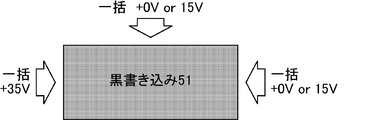
- the orientation of liquid crystal molecules in the vicinity of the edges of a pair of comb electrodes can be suitably controlled, and the transmittance that floats without all electrodes being equipotential can be sufficiently lowered to the initial black state. (For example, a portion surrounded by a dotted line in FIG. 8 described later).
- the initialization step may be one that performs substantially not to cause a potential difference driving operation between all the electrodes, for example, be done by floating at least one of the pair of comb electrodes and the TFT in the OFF state may, instead, or a constant voltage is applied to at least one of the pair of comb electrodes and all the TFT in the oN state, at least the pair of comb electrodes and the TFT in the even lines or odd lines in the oN state Alternatively, a constant voltage may be applied to each of the even and odd lines. Further, the initialization step may be performed after the generation of the vertical electric field, and other electric fields may be generated after the generation of the vertical electric field, but it is preferable that the initialization process is performed immediately after the generation of the vertical electric field.
- a potential difference is usually generated at least between electrodes (for example, a pair of comb electrodes) included in the second substrate.
- electrodes for example, a pair of comb electrodes
- a higher potential difference can be generated between the electrodes of the second substrate than between the electrodes of the first substrate and the electrodes (eg, planar electrodes) of the second substrate.
- the potential of the planar electrode of the first substrate and the potential of the planar electrode of the second substrate are 7.5 V and 0 V, respectively, and the potential of the pair of comb electrodes of the second substrate is 15 V, respectively.
- 0 V, or the potential of the planar electrode of the first substrate and the potential of the planar electrode of the second substrate are 7.5 V and 7.5 V, respectively, and a pair of combs of the second substrate
- the potential of the tooth electrode is set to 15 V and 0 V, respectively, and the potential of the planar electrode of the first substrate and the potential of the planar electrode of the second substrate are set to 0 V and 0 V, respectively.
- the potential of the pair of comb electrodes is 15 V and 0 V, respectively. It can be or.
- a potential difference lower than that between the electrode of the first substrate and the electrode of the second substrate may be generated between the electrodes of the second substrate.
- the potential of the planar electrode included in the first substrate and the potential of the planar electrode included in the second substrate are set to 7.5 V and 0 V, respectively, and the pair of the second substrate includes.
- the potential of the comb-tooth electrode is 10 V, 5 V (inter-comb potential 5 V), respectively.
- the potential change can be reversed by applying to the lower layer electrode (planar electrode of the second substrate) commonly connected to each of the even lines and odd lines.
- the potential of the electrode held at a constant voltage may be an intermediate potential.
- the potential of the electrode held at the constant voltage is considered to be 0 V, the polarity of the voltage applied to the lower layer electrode for each bus line is reversed. It can be said that it is done.
- the first substrate and the second substrate included in the liquid crystal display panel of the present invention are a pair of substrates for sandwiching a liquid crystal layer.
- an insulating substrate such as glass or resin is used as a base, and wiring and electrodes are formed on the insulating substrate. It is formed by making a color filter or the like.
- the liquid crystal display panel of the present invention may be any of a transmissive type, a reflective type, and a transflective type.
- the present invention is also a liquid crystal display device including the liquid crystal display panel of the present invention.
- the preferred form of the liquid crystal display panel in the liquid crystal display device of the present invention is the same as the preferred form of the liquid crystal display panel of the present invention described above.
- Examples of the liquid crystal display device include in-vehicle devices such as personal computers, televisions, and car navigation systems, and displays of portable information terminals such as mobile phones. In particular, in a low-temperature environment such as in-vehicle devices such as car navigation systems. It is preferable to be applied to devices used in the above.
- the present invention is a thin film transistor array substrate having thin film transistor elements, wherein the electrodes of the thin film transistor array substrate include a pair of comb electrodes and a planar electrode, and the group consisting of the pair of comb electrodes and the planar electrode
- the at least one electrode selected is also a thin film transistor array substrate that is electrically connected along the pixel line.
- the planar electrodes are preferably electrically connected along the pixel line. More preferably, the planar electrode is composed of a transparent conductor and a metal conductor that is electrically connected to the transparent conductor. As a result, the resistance of the electrode can be reduced, and the waveform can be sufficiently prevented from becoming distorted. In a large panel, the resistance of the electrode may be too large and the waveform may be distorted, and it is particularly preferable to apply to a large liquid crystal display device in that this can be prevented.
- At least one of the pair of comb electrodes is preferably electrically connected along the pixel line. More preferably, at least one of the pair of comb electrodes is composed of a transparent conductor and a metal conductor electrically connected to the transparent conductor. For the same reason as described above, it is particularly preferable to apply such a liquid crystal driving device to a large liquid crystal display device. Further, it is preferable that at least one of the pair of comb electrodes is electrically connected to the planar electrode.
- the electrode is electrically connected along the pixel line, in other words, the electrode is electrically connected at least for each identical pixel line. May be connected for every one pixel line, or may be connected for every n pixel lines (each n lines), both of which are preferable. Note that n is an integer of 2 or more.
- the electrode is connected to each of a plurality (n) of pixel lines as long as the electrodes corresponding to the plurality of pixel lines are electrically connected. For example, the electrodes are odd-numbered. A form of electrical connection for every pixel line and every even-numbered pixel line is also included.
- the plurality of lines are usually reversed at the same time.
- the thin film transistor array substrate is a thin film transistor array substrate for frame inversion driving or line inversion driving, and at least one electrode selected from the group consisting of the pair of comb electrodes and planar electrodes is one pixel line. It is a preferred form of the present invention that each pixel line is electrically connected to each other. That is, the thin film transistor array substrate can be used for frame inversion driving and line inversion driving. Line inversion driving is more preferable from the viewpoint of making flickers difficult to recognize and improving display quality.
- each pixel line is electrically connected between each pixel of the pixel line as long as the effects of the present invention can be exhibited, all the pixels on the pixel line are electrically connected. It is not necessary to be electrically connected between all the pixels of the pixel line.
- the thin film transistor array substrate is a thin film transistor array substrate for frame inversion driving, line inversion driving or dot inversion driving, and at least one electrode selected from the group consisting of the pair of comb electrodes and planar electrodes is Another preferred embodiment of the present invention is that every other pixel is electrically connected to one pixel line. That is, the thin film transistor array substrate can be used for frame inversion driving, line inversion driving, and dot inversion driving. Line inversion driving and dot inversion driving are more preferable from the viewpoint of making flickers difficult to recognize and improving display quality. Most preferably, dot inversion driving is performed.
- there are two sets of pixels every other pixel for one pixel line but one set of pixels may be electrically connected, and both sets of pixels are electrically connected. It may be connected to. Note that the term “electrically connected between every other pixel in one pixel line” means that there is substantially no electrical connection between every other pixel as long as the effects of the present invention can be exhibited. Just do it.
- the present invention is a thin film transistor array substrate having thin film transistor elements, wherein the electrode of the thin film transistor array substrate includes a pair of comb electrodes and a planar electrode, and at least one of the pair of comb electrodes is a planar shape. It is also a thin film transistor array substrate that is electrically connected to the electrodes.
- the present invention is also a liquid crystal display device comprising the thin film transistor array substrate of the present invention.
- the preferred form of the thin film transistor array substrate in the liquid crystal display device of the present invention is the same as the preferred form of the thin film transistor array substrate of the present invention described above.
- As a liquid crystal display device it can apply suitably for the use mentioned above.
- the configuration of the liquid crystal display device and the thin film transistor array substrate of the present invention is not particularly limited by other components as long as such components are formed as essential, and the liquid crystal display device and the thin film transistor array are not limited. Other configurations usually used for the substrate can be applied as appropriate.
- the first substrate and the second substrate have electrodes, and the electrodes of the second substrate include a pair of comb-tooth electrodes and a planar electrode, thereby sufficiently increasing the response speed.
- the transmittance can be made sufficiently excellent.
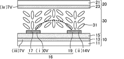
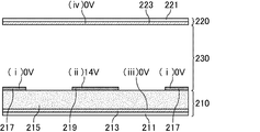
- FIG. 3 is a schematic cross-sectional view of the liquid crystal display panel according to Embodiment 1 when a horizontal electric field is generated.
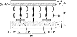
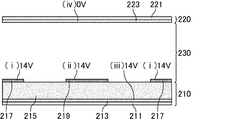
- FIG. 3 is a schematic cross-sectional view of the liquid crystal display panel according to Embodiment 1 when a vertical electric field is generated.
- FIG. 3 is a schematic cross-sectional view of the liquid crystal display panel according to Embodiment 1 when a horizontal electric field is generated.
- FIG. It is a simulation result about the liquid crystal display panel shown in FIG.
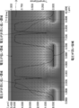
- FIG. 6 is a graph showing measured values of drive response waveforms and applied rectangular waves of each electrode in the first embodiment.
- 6 is a graph showing the relationship between maximum transmittance and cell thickness d in the first embodiment.
- 4 is a graph showing the relationship between maximum transmittance and space S in the first embodiment.
- 6 is a schematic cross-sectional view of a liquid crystal display panel according to Embodiment 2 when a horizontal electric field is generated.
- FIG. 6 is a schematic cross-sectional view of a liquid crystal display panel according to Embodiment 2 when a vertical electric field is generated.
- FIG. 10 is a graph showing a rectangular wave (driving waveform) applied to each electrode in the second embodiment.
- FIG. 6 is a schematic cross-sectional view of a liquid crystal display panel according to Embodiment 3 when a horizontal electric field is generated.
- FIG. 6 is a schematic cross-sectional view of a liquid crystal display panel according to Embodiment 3 when a vertical electric field is generated.
- FIG. 10 is a graph showing an applied rectangular wave (drive waveform) of each electrode in Embodiment 3.
- 6 is a graph showing actual measured values of drive response waveforms in the first to third embodiments.
- 1 is a schematic cross-sectional view of a liquid crystal display panel according to Embodiment 1.
- FIG. 4 is a schematic plan view of picture elements of the liquid crystal display panel according to Embodiment 1.
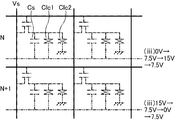
- FIG. 3 is a picture element equivalent circuit diagram of the liquid crystal display panel according to Embodiment 1.
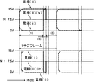
- FIG. 3 is a diagram illustrating a potential change of each electrode of the liquid crystal display panel according to the first embodiment.
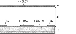
- FIG. 3 is a schematic cross-sectional view showing each electrode of the Nth row when a horizontal electric field is generated in the liquid crystal display panel according to Embodiment 1.
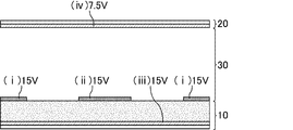
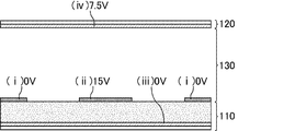
- FIG. 3 is a schematic cross-sectional view showing each electrode of the Nth row when a vertical electric field is generated in the liquid crystal display panel according to Embodiment 1.
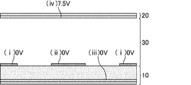
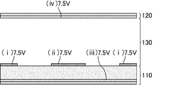
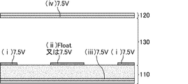
- FIG. 4 is a schematic cross-sectional view showing each electrode in the Nth row in an initialization process after the occurrence of a vertical electric field in the liquid crystal display panel according to Embodiment 1.
- FIG. 3 is a diagram illustrating a potential change of each electrode of the liquid crystal display panel according to the first embodiment.
- FIG. 3 is a schematic cross-sectional view showing each electrode of the Nth row when a horizontal electric field is generated in the liquid crystal display panel according to Embodiment 1.
- FIG. 3 is a schematic cross-sectional view showing each electrode
- FIG. 3 is a schematic cross-sectional view showing each electrode in the (N + 1) th row when a horizontal electric field is generated in the liquid crystal display panel according to Embodiment 1.
- FIG. 3 is a schematic cross-sectional view showing each electrode in the (N + 1) th row when a vertical electric field is generated in the liquid crystal display panel according to Embodiment 1.
- FIG. 3 is a schematic cross-sectional view showing each electrode of the (N + 1) th row in the initialization process after the vertical electric field is generated in the liquid crystal display panel according to Embodiment 1.
- 6 is a schematic cross-sectional view of a liquid crystal display panel according to Embodiment 2.
- FIG. 6 is a schematic plan view of picture elements of a liquid crystal display panel according to Embodiment 2.
- FIG. 1 is a schematic cross-sectional view showing each electrode in the (N + 1) th row when a horizontal electric field is generated in the liquid crystal display panel according to Embodiment 1.
- FIG. 3 is a schematic cross
- FIG. 6 is a picture element equivalent circuit diagram of a liquid crystal display panel according to Embodiment 2.
- FIG. FIG. 6 is a diagram showing a potential change of each electrode of a liquid crystal display panel according to Embodiment 2.
- 10 is a schematic cross-sectional view showing each electrode of the Nth row when a horizontal electric field is generated in the liquid crystal display panel according to Embodiment 2.
- FIG. 10 is a schematic cross-sectional view illustrating each electrode in the Nth row in an initialization process after generation of a horizontal electric field in the liquid crystal display panel according to Embodiment 2.
- FIG. 10 is a schematic cross-sectional view showing each electrode of the Nth row when a vertical electric field is generated in the liquid crystal display panel according to Embodiment 2.
- FIG. 10 is a schematic cross-sectional view showing each electrode in the Nth row in an initialization process after generation of a vertical electric field in the liquid crystal display panel according to Embodiment 2.
- FIG. 10 is a schematic cross-sectional view showing each electrode of the (N + 1) th row when a horizontal electric field is generated in the liquid crystal display panel according to Embodiment 2.
- FIG. 10 is a schematic cross-sectional view showing each electrode in the (N + 1) th row in an initialization process after generation of a horizontal electric field in the liquid crystal display panel according to Embodiment 2.
- FIG. 10 is a schematic cross-sectional view showing each electrode of the (N + 1) th row when a vertical electric field is generated in the liquid crystal display panel according to Embodiment 2.
- FIG. 10 is a schematic cross-sectional view showing each electrode of the (N + 1) th row when a vertical electric field is generated in the liquid crystal display panel according to Embodiment 2.
- FIG. 10 is a schematic cross-sectional view showing each electrode of the (N + 1) th row in an initialization process after generation of a vertical electric field in the liquid crystal display panel according to Embodiment 2.
- 10 is a schematic cross-sectional view of a liquid crystal display panel according to a modification of Embodiment 2.
- FIG. 11 is a schematic plan view of picture elements of a liquid crystal display panel according to a modification of the second embodiment.
- FIG. 10 is a picture element equivalent circuit diagram of a liquid crystal display panel according to a modification of the second embodiment.
- FIG. 10 is a diagram illustrating a potential change of each electrode of a liquid crystal display panel according to a modification of the second embodiment.
- FIG. 10 is a schematic cross-sectional view showing each electrode in the Nth row when a horizontal electric field is generated in a liquid crystal display panel according to a modification of the second embodiment.
- FIG. 10 is a schematic cross-sectional view showing each electrode in the Nth row when a vertical electric field is generated in a liquid crystal display panel according to a modification of the second embodiment.
- FIG. 10 is a schematic cross-sectional view showing each electrode in the Nth row in an initialization process after the occurrence of a vertical electric field in a liquid crystal display panel according to a modification of Embodiment 2.
- FIG. 10 is a schematic cross-sectional view showing each electrode in the (N + 1) th row when a horizontal electric field is generated in a liquid crystal display panel according to a modification of the second embodiment.
- FIG. 10 is a schematic cross-sectional view showing each electrode of the (N + 1) th row when a vertical electric field is generated in a liquid crystal display panel according to a modification of Embodiment 2.
- FIG. 11 is a schematic cross-sectional view showing each electrode of the (N + 1) th row in an initialization process after a vertical electric field is generated in a liquid crystal display panel according to a modification of Embodiment 2.
- 6 is a schematic cross-sectional view of a liquid crystal display panel according to Embodiment 3.
- FIG. 6 is a schematic plan view of picture elements of a liquid crystal display panel according to Embodiment 3.
- FIG. 6 is a picture element equivalent circuit diagram of a liquid crystal display panel according to Embodiment 3.
- FIG. 10 is a schematic cross-sectional view showing each electrode of the Nth row when a horizontal electric field is generated in the liquid crystal display panel according to Embodiment 3.
- FIG. 10 is a schematic cross-sectional view showing each electrode of the Nth row when a vertical electric field is generated in the liquid crystal display panel according to Embodiment 3.
- FIG. 10 is a schematic cross-sectional view showing each electrode of the Nth row in an initialization process after generation of a vertical electric field in the liquid crystal display panel according to Embodiment 3.
- FIG. 10 is a schematic cross-sectional view showing each electrode of the Nth row in an initialization process after generation of a vertical electric field in the liquid crystal display panel according to Embodiment 3.
- FIG. 10 is a schematic cross-sectional view showing each electrode in the (N + 1) th row when a horizontal electric field is generated in the liquid crystal display panel according to Embodiment 3.
- FIG. 10 is a schematic cross-sectional view showing each electrode in the (N + 1) th row when a vertical electric field is generated in the liquid crystal display panel according to Embodiment 3.
- FIG. 10 is a schematic cross-sectional view showing each electrode in the (N + 1) th row in an initialization process after generation of a vertical electric field in the liquid crystal display panel according to Embodiment 3. It is a plane schematic diagram which shows the drive form of the liquid crystal display panel of this invention. It is a plane schematic diagram which shows the drive form of the liquid crystal display panel of this invention.
- FIG. 67 is a schematic plan view of the liquid crystal display panel shown in FIG. 64.
- 65 is a simulation result on the liquid crystal display panel shown in FIG. 64.
- It is a graph which shows the response waveform by the simulation of the comb drive using the TN mode in the comparative example 2. It is a simulation result about the liquid crystal display panel which concerns on the comparative example 2.
- FIG. It is a simulation result about the liquid crystal display panel which concerns on the comparative example 2.
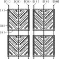
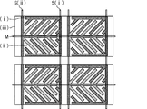
- FIG. It is a cross-sectional schematic diagram which shows one form of the comb-tooth electrode of the liquid crystal display panel which concerns on this invention. It is a cross-sectional schematic diagram which shows one form of the comb-tooth electrode of the liquid crystal display panel which concerns on this invention. It is a plane schematic diagram which shows one form of the design pattern of the drive device of the invention relevant to this invention. It is a plane schematic diagram which shows one form of the design pattern of the drive device of this invention. It is a plane schematic diagram which shows one form of the design pattern of the drive device of this invention. It is a plane schematic diagram which shows one form of the design pattern of the drive device of this invention. It is a plane schematic diagram which shows one form of the design pattern of the drive device of this invention. It is a plane schematic diagram which shows one form of the design pattern of the drive device of this invention.
- a pixel may be a picture element (sub-pixel) unless otherwise specified.
- a subframe refers to a frame that is displayed by all pixels (for example, pixels including RGB), for example, in one frame by field sequential (time division) driving using some or all picture elements.
- the time spent for displaying one color is referred to as a period for the display in this specification.
- the planar electrode is a planar electrode in the technical field of the present invention, for example, dot-shaped ribs and / or slits may be formed, but the planar electrode has a substantially alignment regulating structure. What is not preferred is preferred.
- the substrate on the display surface side is also referred to as an upper substrate, and the substrate on the opposite side to the display surface is also referred to as a lower substrate.
- the electrodes arranged on the substrate the electrode on the display surface side is also referred to as an upper layer electrode, and the electrode on the opposite side to the display surface is also referred to as a lower layer electrode.
- the circuit substrate (second substrate) of this embodiment is also referred to as a TFT substrate or an array substrate because it includes a thin film transistor element (TFT).
- the TFT is turned on and a voltage is applied to at least one electrode (pixel electrode) of the pair of comb-teeth electrodes, both at the rise (horizontal electric field application) and the fall (vertical electric field application). ing.
- the member and part which exhibit the same function are attached
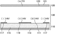
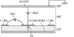
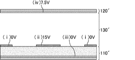
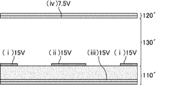
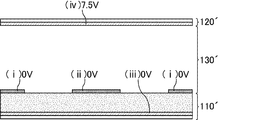
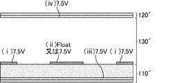
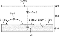
- (i) shows the potential of one of the comb-shaped electrodes on the upper layer of the lower substrate, and (ii) shows the other potential of the comb-shaped electrode on the upper layer of the lower substrate.
- (Iii) shows the potential of the planar electrode on the lower layer of the lower substrate, and (iv) shows the potential of the planar electrode on the upper substrate.
- FIG. 1 is a schematic cross-sectional view of the liquid crystal display panel according to Embodiment 1 when a lateral electric field is generated.
- FIG. 2 is a schematic cross-sectional view of the liquid crystal display panel according to Embodiment 1 when a vertical electric field is generated. 1 and 2, the dotted line indicates the direction of the generated electric field.
- the liquid crystal display panel according to the first embodiment, the liquid crystal molecules 31 is a positive liquid crystal three-layer electrode structure (here vertically oriented type using, upper electrode of the lower substrate located in the second layer is comb electrodes ). As shown in FIG.
- the rise is caused by a lateral electric field generated by a potential difference of 14 V between a pair of comb electrodes 16 (for example, a comb electrode 17 having a potential of 0 V and a comb electrode 19 having a potential of 14 V). Rotate the liquid crystal molecules. At this time, a potential difference between the substrates (between the counter electrode 13 having a potential of 7V and the counter electrode 23 having a potential of 7V) does not substantially occur.
- the fall occurs between the substrates (for example, between the counter electrode 13, the comb electrode 17 and the comb electrode 19 each having a potential of 14 V, and the counter electrode 23 having a potential of 7 V.
- the liquid crystal molecules are rotated by a vertical electric field generated at a potential difference of 7V.
- there is substantially no potential difference between the pair of comb-shaped electrodes 16 for example, the comb-shaped electrode 17 having a potential of 14V and the comb-shaped electrode 19 having a potential of 14V).
- High-speed response is achieved by rotating liquid crystal molecules by an electric field for both rising and falling. That is, at the rising edge, the lateral electric field between the pair of comb electrodes is turned on to increase the transmittance, and at the falling edge, the vertical electric field between the substrates is turned on to increase the response speed. Further, a high transmittance can be realized by a lateral electric field driven by a comb.
- a positive liquid crystal is used as the liquid crystal, but a negative liquid crystal may be used instead of the positive liquid crystal.
- the liquid crystal molecules are aligned in the horizontal direction due to the potential difference between the pair of substrates, and the liquid crystal molecules are aligned in the vertical direction due to the potential difference between the pair of comb electrodes.
- the transmittance is excellent, and the liquid crystal molecules can be rotated by an electric field at both rising and falling, thereby achieving high-speed response.
- the effect of sufficiently reducing the transmittance during black display can be exhibited as in the case of the positive type liquid crystal.
- At least a driving operation for generating a potential difference between the opposing electrodes disposed on each of the upper and lower substrates a driving operation for generating a potential difference between the electrodes of at least one pair of comb-tooth electrodes, the counter electrode and the pair of comb teeth It is preferable to execute in the order of driving operations that do not cause a potential difference between the electrodes.
- the potential of the pair of comb electrodes is indicated by (i) and (ii)
- the potential of the planar electrode of the lower substrate is indicated by (iii)
- the potential of the planar electrode of the upper substrate is ( iv).
- the liquid crystal display panel according to the first embodiment as shown in FIGS. 1 and 2, the array substrate 10, the liquid crystal layer 30 and the counter substrate 20 (color filter substrate), the viewing surface side from the back side of the liquid crystal display panel
- the layers are stacked in this order.
- the liquid crystal display panel of Embodiment 1 vertically aligns liquid crystal molecules below a threshold voltage.
- the voltage difference between the comb electrodes when the voltage difference between the comb electrodes is equal to or higher than the threshold voltage, it is generated between the upper layer electrodes 17 and 19 (a pair of comb electrodes) formed on the glass substrate 11 (second substrate).
- the transmitted light amount is controlled by tilting the liquid crystal molecules in the horizontal direction between the comb-teeth electrodes with an electric field.
- the planar lower electrode 13 (counter electrode 13) is formed with the insulating layer 15 sandwiched between the upper electrodes 17 and 19 (a pair of comb electrodes 16).
- the insulating layer 15 for example, an oxide film SiO 2 , a nitride film SiN, an acrylic resin, or the like can be used, or a combination of these materials can also be used.
- a polarizing plate is disposed on the opposite side of the liquid crystal layers of both substrates.
- the polarizing plate either a circular polarizing plate or a linear polarizing plate can be used.
- alignment films are arranged on the liquid crystal layer side of both substrates, and these alignment films are either organic alignment films or inorganic alignment films as long as the liquid crystal molecules stand vertically with respect to the film surfaces. There may be.
- a voltage supplied from the video signal line is applied to the comb electrode 19 that drives the liquid crystal material through a thin film transistor element (TFT).
- TFT thin film transistor element
- the comb-teeth electrode 17 and the comb-teeth electrode 19 are formed in the same layer, and a form in which the comb-teeth electrode 17 and the comb-teeth electrode 19 are formed in the same layer is preferable. As long as the effect of the present invention of improving the transmittance by applying an electric field can be exhibited, it may be formed in a separate layer.
- the comb electrode 19 is connected to a drain electrode extending from the TFT through a contact hole.
- the counter electrodes 13 and 23 have a planar shape, and the counter electrode 13 is commonly connected to each of the even and odd lines of the gate bus line. Such an electrode is also referred to as a planar electrode in this specification.
- the counter electrode 23 is connected in common to all the pixels.
- the electrode width L of the comb-tooth electrode is 2.4 ⁇ m, but for example, 2 ⁇ m or more is preferable.
- the electrode spacing S of the comb electrodes is 2.6 ⁇ m, but preferably 2 ⁇ m or more, for example.
- a preferable upper limit is, for example, 7 ⁇ m.
- the ratio (L / S) between the electrode spacing S and the electrode width L is preferably 0.4 to 3, for example.
- a more preferable lower limit value is 0.5, and a more preferable upper limit value is 1.5.
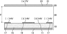
- the cell gap d is 5.4 ⁇ m, but may be 2 ⁇ m to 7 ⁇ m, and is preferably within the range.
- the cell gap d thickness of the liquid crystal layer
- the cell gap d is preferably calculated by averaging all the thicknesses of the liquid crystal layers in the liquid crystal display panel.
- FIG. 3 is a schematic cross-sectional view of the liquid crystal display panel according to Embodiment 1 when a lateral electric field is generated.
- a transverse electric field between a pair of comb electrodes 16 (for example, a comb electrode 17 having a potential of 0 V and a comb electrode 19 having a potential of 14 V)
- FIG. 4 shows simulation results for the liquid crystal display panel shown in FIG.
- FIG. 4 shows the simulation results of the director D, the electric field, and the transmittance distribution at the point of 2.2 ms after the rise (note that the first 0.4 ms is driven as shown in the graphs described later). Not.)
- the graph indicated by the solid line indicates the transmittance.
- Director D indicates the alignment direction of the major axis of the liquid crystal molecule.
- the cell thickness was 5.4 ⁇ m
- the comb-teeth spacing was 2.6 ⁇ m.
- FIG. 5 is a schematic cross-sectional view of the liquid crystal display panel according to Embodiment 1 when a vertical electric field is generated.
- FIG. 6 shows simulation results for the liquid crystal display panel shown in FIG.
- FIG. 6 shows a simulation result at the time point of 3.5 ms after the end point of the rising period (time point of 2.8 ms) of the director D, the electric field, and the transmittance distribution.
- FIG. 7 is a graph comparing response waveforms obtained by simulation of comb tooth drive and FFS drive. Since the first 0.4 ms period is not driven, the rising period (horizontal electric field application period) is 2.4 ms, and the falling period (vertical electric field application period) is 0.8 ms.
- Comb drive (Embodiment 1) is compared with FFS drive (Comparative Example 1) described later. The simulation conditions were performed with a cell thickness of 5.4 ⁇ m and an electrode interval of a pair of comb-teeth electrodes of 2.6 ⁇ m.
- the response speed can be considered as follows.
- the transmittance (18.6%) obtained by the comb driving according to the first embodiment is higher than that of the FFS driving (3.6%) according to Comparative Example 1. Therefore, when trying to obtain a transmittance of 3.6% with the comb drive according to the first embodiment, a faster response can be realized by using the overdrive drive as compared with the FFS drive. That is, by applying a voltage higher than the rated voltage necessary to obtain a transmittance of 3.6% by at least comb driving, the liquid crystal is made to respond quickly and reaches the rated voltage at the timing when the desired transmittance is reached. By reducing the applied voltage, the rise response time can be shortened. For example, in FIG. 7, the response time of the rise can be shortened by reducing the voltage to the rated voltage at the time 41 of 0.6 ms. Fall response times from the same transmittance are equivalent.
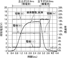
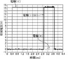
- FIG. 8 is a graph showing the measured drive response waveform and the applied rectangular wave of each electrode in the first embodiment.
- the evaluation cell had a cell thickness of 5.4 ⁇ m, and the distance between the pair of comb electrodes was 2.6 ⁇ m.
- the measurement temperature was 25 ° C.
- a voltage was applied to the electrodes as shown in FIGS. 3 and 5, and a horizontal electric field and a vertical electric field were applied to the liquid crystal molecules, respectively.
- the rising period is 2.4 ms when the comb teeth are driven between the pair of comb electrodes (Embodiment 1)
- the falling period is the pair of comb electrodes, the lower layer electrode of the lower substrate, and the upper side
- a longitudinal electric field drive between the counter electrodes of the substrate is 0.8 ms (see FIG. 8 for the applied waveform of each electrode) )Met.
- the maximum transmittance is 17.7% in the first embodiment (the transmittance in the simulation is 18.6%), which is higher than the comparative example 1 (simulation transmittance 3.6%) described later.
- the rise is 10% -90% transmittance (value when the maximum transmittance is 100%) and the response speed is 0.9 ms, and the fall is 90-10% transmittance (when the maximum transmittance is 100%). Value) of 0.4 ms, and both rising and falling speeds were realized.
- the preferred comb electrode width (L; Line), comb electrode spacing (S; Space), and cell thickness (d) for the longitudinal electric field on-lateral electric field on in the first embodiment were studied.
- the transmittance increases in proportion to the decrease in the comb electrode width L.
- the comb electrode width L is too small, problems such as leakage and disconnection occur in device fabrication. .
- FIG. 9 is a graph showing the relationship between the maximum transmittance and the cell thickness d in the first embodiment.
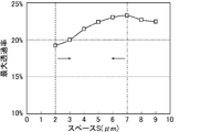
- FIG. 10 is a graph showing the relationship between the maximum transmittance and the space S in the first embodiment.
- both the cell thickness d and the space S are from 2 ⁇ m.
- the maximum transmittance increased as the value increased, but decreased significantly when the value exceeded 7 ⁇ m. Therefore, the cell thickness d and the space S are desirably 7 ⁇ m or less. Therefore, both the cell thickness d and the space S are desirably 2 ⁇ m or more and 7 ⁇ m or less.
- FIG. 11 is a schematic cross-sectional view of the liquid crystal display panel according to Embodiment 2 when a horizontal electric field is generated.
- FIG. 12 is a schematic cross-sectional view of the liquid crystal display panel according to Embodiment 2 when a vertical electric field is generated.
- FIG. 13 is a graph showing a rectangular wave (driving waveform) applied to each electrode in the second embodiment.
- the counter electrode 13 and the counter electrode 23 apply the intermediate voltage (7 V) of the voltage difference (14 V) between the pair of comb electrodes.
- the counter electrode 113 is set to the same potential as the comb electrode 117 that is one side of the pair of comb electrodes, and the counter electrode 123 is set to an intermediate voltage (14V) between the pair of comb electrodes. 7V) (Embodiment 2), and other configurations are the same as those in Embodiment 1.
- FIG. 14 is a schematic cross-sectional view of the liquid crystal display panel according to Embodiment 3 when a horizontal electric field is generated.
- FIG. 15 is a schematic cross-sectional view of the liquid crystal display panel according to Embodiment 3 when a vertical electric field is generated.
- FIG. 16 is a graph showing a rectangular wave (driving waveform) applied to each electrode in the third embodiment.
- the counter electrode 213 is set to the same potential as the comb electrode 217, which is one side of the pair of comb electrodes, and the counter electrode 223 is set to 0 V.
- Other configurations are the same as those in the first embodiment. It is the same.
- FIG. 17 is a graph showing actual measured values of drive response waveforms in the first to third embodiments.
- the response performance and the transmittance were measured as in the first embodiment.
- the evaluation cell has a cell thickness of 5.4 ⁇ m, and the electrode interval between the pair of comb electrodes is 2.6 ⁇ m.
- the measurement temperature was 25 ° C.
- in the first embodiment in the second and third embodiments, as shown in FIG. 17, as compared with Comparative Example 1 (simulation transmittance 3.6%) while maintaining high-speed response. It was confirmed that high response performance and high transmittance can be achieved.
- FIG. 18 is a schematic cross-sectional view of the liquid crystal display panel according to the first embodiment.
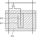
- FIG. 19 is a schematic plan view of picture elements of the liquid crystal display panel according to the first embodiment.
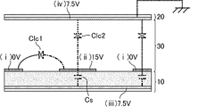
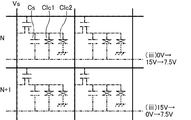
- FIG. 20 is a pixel equivalent circuit diagram of the liquid crystal display panel according to the first embodiment.
- FIG. 21 is a diagram illustrating a change in potential of each electrode of the liquid crystal display panel according to the first embodiment. As a driving method with the module in the first embodiment, two TFTs are driven per picture element. In FIG. 18 to FIG. 21, the wiring electrically connected to the lower layer electrode of the lower substrate is indicated by a two-dot chain line.
- a wiring electrically connected to one of the pair of comb electrodes on the lower substrate is indicated by a one-dot chain line.
- a wiring electrically connected to the other of the pair of comb electrodes on the lower substrate is represented by a dotted line having a narrower interval in the drawing.
- Wirings electrically connected to the electrodes of the upper substrate are represented by dotted lines with wider intervals in the drawing.
- the lower layer electrode also serves as the Cs electrode, and is commonly connected to each of the even line and the odd line.
- the auxiliary capacitance formed by the overlap of the comb-tooth electrode and the Cs electrode is indicated by Cs
- the liquid crystal capacitance formed between the pair of comb-tooth electrodes is indicated by Clc1
- Clc2 the liquid crystal capacitance formed between the pair of comb-tooth electrodes
- Clc2 the liquid crystal capacitance formed between the pair of comb-tooth electrodes.
- Clc2 the formed liquid crystal capacitance.
- the voltage applied to the lower layer electrode is 7.5V during bright display, then 15V during dark display (black display), and 7.5V during the initialization process.
- the voltage applied to the lower layer electrode is 7.5V during bright display, then becomes 0V during dark display (black display), and becomes 7.5V during the initialization process. Yes.
- the Nth row may be an even line
- the N + 1th row may be an odd line
- the Nth row may be an odd line
- the N + 1th row may be an even line.
- the potential change is reversed by applying to the lower layer electrode commonly connected to each of the even and odd lines. Note that although the potential of the electrode held at a constant voltage is expressed as 7.5 V, this can be said to be substantially 0 V, and thus it can be said that the N line and the N + 1 line are driven with the polarity reversed.
- FIG. 22 is a schematic cross-sectional view showing each electrode in the Nth row when the horizontal electric field is generated in the liquid crystal display panel according to Embodiment 1.
- FIG. 23 is a schematic cross-sectional view showing each electrode in the Nth row when the vertical electric field is generated in the liquid crystal display panel according to Embodiment 1.
- FIG. 24 is a schematic cross-sectional view showing each electrode in the Nth row in the initialization process after the vertical electric field is generated in the liquid crystal display panel according to Embodiment 1.
- FIG. 25 is a schematic cross-sectional view showing each electrode in the (N + 1) th row when the horizontal electric field is generated in the liquid crystal display panel according to the first embodiment.
- FIG. 26 is a schematic cross-sectional view showing each electrode in the (N + 1) th row when the vertical electric field is generated in the liquid crystal display panel according to Embodiment 1.
- FIG. 27 is a schematic cross-sectional view showing each electrode of the (N + 1) th row in the initialization process after the vertical electric field is generated in the liquid crystal display panel according to Embodiment 1.
- the liquid crystal is driven by a lateral electric field between a pair of comb electrodes.
- a vertical electric field is applied with both the comb-tooth electrode and the lower layer electrode set to 15 V or 0 V (TFTs are turned on for each even line / odd line).
- the TFTs are turned off and the pair of comb electrodes are floated, or all the TFTs are turned on and the pair of comb electrodes are set to 7.5V, and the lower layer electrode is 7.5V.
- the initial orientation is refreshed (initialization process).
- the liquid crystal display device provided with the liquid crystal display panel of Embodiment 1 can appropriately include a member (for example, a light source or the like) included in a normal liquid crystal display device. The same applies to the embodiments described later.
- FIG. 28 is a schematic cross-sectional view of a liquid crystal display panel according to the second embodiment.
- FIG. 29 is a schematic plan view of picture elements of a liquid crystal display panel according to the second embodiment.
- FIG. 30 is a picture element equivalent circuit diagram of the liquid crystal display panel according to the second embodiment.
- FIG. 31 is a diagram illustrating a potential change of each electrode of the liquid crystal display panel according to the second embodiment. As a driving method using a module in the second embodiment, one TFT is driven per picture element.
- the wiring electrically connected to the lower layer electrode of the lower substrate is indicated by a two-dot chain line.
- a wiring electrically connected to one of the pair of comb electrodes on the lower substrate is indicated by a one-dot chain line.
- the wiring electrically connected to the other of the pair of comb electrodes on the lower substrate is indicated by a two-dot chain line because the other of the comb electrodes is electrically connected to the lower electrode of the lower substrate.
- a wiring electrically connected to the electrode of the upper substrate is represented by a dotted line.
- the lower layer electrode also serves as the Cs electrode, and is commonly connected to each of the even line and the odd line.
- the voltage applied to the lower layer electrode is 0 V during bright display, and then after an initialization process of 7.5 V (all TFTs on) during dark display (black display), At the time of application, it is 15V, and in the initialization process after application of the vertical electric field, it is 7.5V.
- the voltage applied to the lower layer electrode is 15 V during bright display, and then after an initialization process of 7.5 V (all TFTs on) in dark display (black display), The voltage is 0 V when the vertical electric field is applied, and 7.5 V in the initialization process after the vertical electric field is applied.
- the Nth row may be an even line
- the N + 1th row may be an odd line
- the Nth row may be an odd line
- the N + 1th row may be an even line.
- the potential change is inverted by applying to the lower layer electrode commonly connected to each of the even and odd lines. Note that although the potential of the electrode held at a constant voltage is expressed as 7.5 V, this can be said to be substantially 0 V, so that it can be said that the N line and the N + 1 line are driven with the polarity reversed.
- FIG. 32 is a schematic cross-sectional view showing each electrode in the Nth row when a horizontal electric field is generated in the liquid crystal display panel according to the second embodiment.
- FIG. 33 is a schematic cross-sectional view showing each electrode in the Nth row in the initialization process after the generation of the horizontal electric field in the liquid crystal display panel according to Embodiment 2.
- FIG. 34 is a schematic cross-sectional view showing each electrode in the Nth row when a vertical electric field is generated in the liquid crystal display panel according to the second embodiment.
- FIG. 35 is a schematic cross-sectional view illustrating each electrode in the Nth row in the initialization process after the vertical electric field is generated in the liquid crystal display panel according to the second embodiment.
- FIG. 36 is a schematic cross-sectional view showing each electrode of the (N + 1) th row when the horizontal electric field is generated in the liquid crystal display panel according to the second embodiment.
- FIG. 37 is a schematic cross-sectional view showing each electrode of the (N + 1) th row in the initialization process after the generation of the horizontal electric field in the liquid crystal display panel according to the second embodiment.
- FIG. 38 is a schematic cross-sectional view showing each electrode in the (N + 1) th row when a vertical electric field is generated in the liquid crystal display panel according to the second embodiment.
- FIG. 39 is a schematic cross-sectional view showing each electrode of the (N + 1) th row in the initialization process after the vertical electric field is generated in the liquid crystal display panel according to the second embodiment.
- the liquid crystal is driven by a lateral electric field between a pair of comb electrodes.
- all TFTs are turned on and all electrodes are once reset to 7.5V.
- 34 and 38 the TFT is turned off to float one of the pair of comb-teeth electrodes, or the TFT is turned on for every even line / odd line and one of the pair of comb-teeth electrodes is set to 15V or 0V.
- the vertical electric field is applied with the lower electrode set at 15V or 0V.
- the TFT is turned off and one of the pair of comb electrodes is floated, or all the TFTs are turned on and the pair of comb electrodes are set to 7.5V, and the lower electrode 7.5V is initially set.
- the alignment is refreshed (initialization process).
- Other reference numerals in the drawing according to the second embodiment are the same as those shown in the drawing according to the first embodiment except that 1 is added to the hundreds place.
- FIG. 40 is a schematic cross-sectional view of a liquid crystal display panel according to a modification example of the second embodiment.
- FIG. 41 is a schematic plan view of picture elements of a liquid crystal display panel according to a modification of the second embodiment.
- FIG. 42 is a pixel equivalent circuit diagram of a liquid crystal display panel according to a modification of the second embodiment.
- FIG. 43 is a diagram illustrating a potential change of each electrode of the liquid crystal display panel according to the modification of the second embodiment.
- the wiring electrically connected to the lower layer electrode of the lower substrate is indicated by a two-dot chain line.
- a wiring electrically connected to one of the pair of comb electrodes on the lower substrate is indicated by a one-dot chain line.
- the wiring electrically connected to the other of the pair of comb electrodes on the lower substrate is indicated by a two-dot chain line because the other of the comb electrodes is electrically connected to the lower electrode of the lower substrate.
- a wiring electrically connected to the electrode of the upper substrate is represented by a dotted line.
- the lower layer electrode also serves as the Cs electrode, and is commonly connected to each of the even line and the odd line. In the picture element in the Nth row, the voltage applied to the lower layer electrode is 0 V during bright display, then 15 V during dark display (black display), and in the initialization process for dark display (black display), 7. It is 5V.
- the voltage applied to the lower layer electrode is 15 V during bright display, then becomes 0 V during dark display (black display), and in the initialization process where dark display (black display) is performed. It is 7.5V.
- the Nth row may be an even line
- the N + 1th row may be an odd line
- the Nth row may be an odd line
- the N + 1th row may be an even line.
- the potential change is inverted by applying to the lower layer electrode connected in common for each of the even and odd lines. Note that although the potential of the electrode held at a constant voltage is expressed as 7.5 V, this can be said to be substantially 0 V, so that it can be said that the N line and the N + 1 line are driven with the polarity reversed.
- FIG. 44 is a schematic cross-sectional view showing each electrode in the Nth row when a horizontal electric field is generated in a liquid crystal display panel according to a modification of the second embodiment.
- FIG. 45 is a schematic cross-sectional view showing each electrode in the Nth row when a vertical electric field is generated in a liquid crystal display panel according to a modification of the second embodiment.
- FIG. 46 is a schematic cross-sectional view showing each electrode in the Nth row in the initialization process after the vertical electric field is generated in the liquid crystal display panel according to the modification of the second embodiment.
- FIG. 47 is a schematic cross-sectional view showing each electrode in the (N + 1) th row when a horizontal electric field is generated in the liquid crystal display panel according to the modification of the second embodiment.
- FIG. 48 is a schematic cross-sectional view showing each electrode of the (N + 1) th row when a vertical electric field is generated in the liquid crystal display panel according to the modification of the second embodiment.
- FIG. 49 is a schematic cross-sectional view showing each electrode of the (N + 1) th row in the initialization process after the vertical electric field is generated in the liquid crystal display panel according to the modification of the second embodiment.
- the liquid crystal is driven by a lateral electric field between a pair of comb electrodes.
- the TFT is turned on for each even line / odd line, and the vertical electric field is applied with both the comb electrode and the lower layer electrode set to 15V or 0V.
- the TFT is turned off to float one of the pair of comb electrodes, or the entire TFT is turned on to set the pair of comb electrodes to 7.5V and the lower layer electrode to 7.5V.
- the initial orientation is refreshed (initialization process).
- the other reference numbers of the figure which concerns on the modification of Embodiment 2 are the same as what was shown to the figure which concerns on Embodiment 1 except having attached 1 to the hundreds place and attaching "'". .
- FIG. 50 is a schematic cross-sectional view of a liquid crystal display panel according to Embodiment 3.
- FIG. 51 is a schematic plan view of picture elements of a liquid crystal display panel according to Embodiment 3.
- FIG. 52 is a pixel equivalent circuit diagram of the liquid crystal display panel according to the third embodiment.
- FIG. 53 is a diagram illustrating a potential change of each electrode of the liquid crystal display panel according to the third embodiment. As a driving method by the module in the third embodiment, one TFT is driven per picture element. 50 to 53, the wiring electrically connected to the lower layer electrode of the lower substrate is indicated by a two-dot chain line.
- a wiring electrically connected to one of the pair of comb electrodes on the lower substrate is indicated by a one-dot chain line.
- the wiring electrically connected to the other of the pair of comb electrodes on the lower substrate is indicated by a two-dot chain line because the other of the comb electrodes is electrically connected to the lower layer electrode of the lower substrate.
- a wiring electrically connected to the electrode of the upper substrate is represented by a dotted line.
- the lower layer electrode also serves as the Cs electrode, and is commonly connected to each of the even line and the odd line. Further, in the third embodiment, the counter electrode on the counter substrate side is also commonly connected for every even line / odd line.
- the voltage applied to the lower layer electrode is 0 V during bright display, and then 15 V during dark display (black display).
- the voltage applied to the lower layer electrode is 15 V during bright display, and then 0 V during dark display (black display).
- the voltage applied to the counter electrode on the counter substrate side is 0V during bright display and is maintained during dark display (black display) thereafter, but is 15V during the initialization process. The potential change is reversed.
- the voltage applied to the counter electrode on the counter substrate side is 15 V during bright display and is maintained during dark display (black display) after that, but is 0 V during the initialization process.
- the potential change is reversed.
- the Nth row may be an even line
- the N + 1th row may be an odd line
- the Nth row may be an odd line
- the N + 1th row may be an even line.
- the potential change is inverted by applying the voltage to the lower electrode and the counter electrode on the counter substrate side that are commonly connected to the even lines and the odd lines.
- FIG. 54 is a schematic cross-sectional view showing each electrode in the Nth row when a horizontal electric field is generated in the liquid crystal display panel according to Embodiment 3.
- FIG. 55 is a schematic cross-sectional view showing each electrode in the Nth row when a vertical electric field is generated in the liquid crystal display panel according to Embodiment 3.
- FIG. 56 is a schematic cross-sectional view showing each electrode in the Nth row in the initialization step after the vertical electric field is generated in the liquid crystal display panel according to Embodiment 3.
- FIG. 57 is a schematic cross-sectional view showing each electrode of the (N + 1) th row when the horizontal electric field is generated in the liquid crystal display panel according to Embodiment 3.
- FIG. 58 is a schematic cross-sectional view showing each electrode of the (N + 1) th row when a vertical electric field is generated in the liquid crystal display panel according to Embodiment 3.
- FIG. 59 is a schematic cross-sectional view showing each electrode of the (N + 1) th row in the initialization process after the vertical electric field is generated in the liquid crystal display panel according to Embodiment 3.
- the liquid crystal is driven by a lateral electric field between a pair of comb electrodes.
- the TFT is turned on for each even line / odd line, both the comb electrode and the lower layer electrode are set to 15 V or 0 V, and the counter electrode on the counter substrate side is set to 0 V or 15 V to generate a vertical electric field.
- the TFT is turned off to float one of the pair of comb electrodes, or the TFT is turned on every even line / odd line and one of the pair of comb electrodes is set to 15 or 0V.
- the counter electrode of the counter substrate is refreshed to the initial orientation (initialization process) at 15 V or 0 V and the lower electrode is 15 V or 0 V.
- the other reference numerals in the drawing according to the third embodiment are the same as those shown in the drawing according to the first embodiment, except that 2 is added to the hundreds place.
- the liquid crystal display panels of Embodiments 1 to 3 are easy to manufacture and can achieve high-speed response and high transmittance.
- the TFT driving method described above is a method of driving including a subframe that is a driving cycle until the liquid crystal is changed back to the initial state, and a potential difference is generated between the electrodes of the pair of comb electrodes during the subframe cycle.
- a driving operation that generates a potential difference higher than that between the electrodes of the pair of comb electrodes, and a potential difference between all the electrodes of the pair of comb electrodes and the pair of counter electrodes. Performing a drive operation that does not occur.
- a potential difference is substantially generated between the pair of comb electrodes and all the electrodes of the pair of counter electrodes.
- a driving operation that does not occur is performed, and thereby the above-described effects of the present invention can be exhibited, and the alignment of the liquid crystal molecules can be suitably controlled to make the transmittance during black display sufficiently low.
- FIG. 60 is a schematic plan view showing a driving mode of the liquid crystal display panel of the present invention.
- FIG. 60 shows how white display is written on the liquid crystal display panel.
- white writing is applied like vertical line inversion. Black writing is not reversed.
- the gate bus line side is scanned (binary of + 35V and ⁇ 5V).
- the lower layer electrode is also scanned (three values of 7.5V, 15V, and 0V).
- the white (halftone) display is already written, and the white (halftone) display is maintained (display maintenance 41).
- the lower electrode is maintained at 7.5V.
- the voltage of the gate bus line is 35 V, and white (halftone) display is written.
- the lower electrode is also scanned and becomes 7.5V.
- black is written and held.
- the lower layer electrode is 15V.
- Black is also written and held in the pixel 43 'along the fourth bus line from the top.
- the lower layer electrode is 0V.
- the counter electrode 23 is always 7.5V.
- FIG. 61 is a schematic plan view showing a driving mode of the liquid crystal display panel of the present invention.
- FIG. 62 is a schematic plan view showing the drive mode of the liquid crystal display panel of the present invention.
- FIG. 63 is a schematic plan view showing a driving mode of the liquid crystal display panel of the present invention.
- FIG. 64 is a schematic cross-sectional view of the liquid crystal display panel according to Comparative Example 1 when a fringe electric field is generated.
- 65 is a schematic plan view of the liquid crystal display panel shown in FIG.
- FIG. 66 shows simulation results for the liquid crystal display panel shown in FIG.
- FIG. 61 conceptually shows the entire display panel shown in FIG.
- a data signal is applied by display writing and held.
- 35V is applied to the gate bus line
- 7.5V is applied to the lower layer electrode
- the data signal is applied.
- the black maintenance 43 display writing has not yet been performed.
- FIG. 62 and 63 conceptually show the entire display panel on which black writing is performed.
- black is written in a lump without scanning. This increases the writing speed.
- FIG. 63 similarly to display writing, scanning is sequentially performed to write black.
- 15V or 0V input may be performed alternately on the line or on the frame.
- a liquid crystal drive device performs a field sequential drive and is provided with a circularly-polarizing plate.
- field sequential driving internal reflection increases because there is no color filter. This is because the transmittance of the color filter is usually 1/3, and the reflected light passes through the color filter twice, so that if there is a color filter, the internal reflection is about 1/10. For this reason, such internal reflection can be sufficiently reduced by using a circularly polarizing plate.
- the electrode structure and the like of the liquid crystal display device and the thin film transistor array substrate of the present invention can be confirmed by microscopic observation such as SEM (Scanning Electron Microscope) on the TFT substrate and the counter substrate.
- FIG. 64 is a schematic cross-sectional view of the liquid crystal display panel according to Comparative Example 1 when a fringe electric field is generated.
- 65 is a schematic plan view of the liquid crystal display panel shown in FIG.
- FIG. 66 shows simulation results for the liquid crystal display panel shown in FIG. Similar to Patent Document 1, the liquid crystal display panel according to Comparative Example 1 generates a fringe electric field by FFS driving.
- FIG. 66 shows the simulation results (cell thickness 5.4 ⁇ m, slit interval 2.6 ⁇ m) of the director D, the electric field, and the transmittance distribution. Note that the reference numbers in FIG. 64 according to the comparative example 1 are the same as those shown in the drawings according to the first embodiment except that the hundreds are marked with 3.
- the slit electrode is 14V and the opposing planar electrode is 7V.
- the slit electrode may be 5V and the opposing planar electrode may be 0V.
- liquid crystal molecules are rotated by a fringe electric field generated between the upper layer and lower layer electrodes of the lower substrate. .
- the transmittance in the simulation is low, which is 3.6%. The transmittance could not be improved as in the above-described embodiment (see FIG. 66).
- FIG. 67 is a graph showing response waveforms obtained by simulation of comb driving using the TN mode in Comparative Example 2. Since the first 0.4 ms period is not driven, the rising period (horizontal electric field application period) is 2.4 ms, and the falling period (vertical electric field application period) is 1.6 ms.
- FIG. 68 to 70 are simulation results for the liquid crystal display panel according to Comparative Example 2.
- FIG. 68 the simulation result at the time of 2.6 ms of the director D, the electric field, and the transmittance distribution is shown.
- FIG. 69 the simulation result at the time of 4.2 ms of the director D, the electric field, and the transmittance distribution is shown.
- FIG. 70 the simulation result at the time of 5.6 ms of the director D, the electric field, and the transmittance distribution is shown.
- the first 0.4 ms is not driven.
- the graph indicated by the solid line indicates the transmittance.
- Director D indicates the alignment direction of the major axis of the liquid crystal molecule.
- Comparative Example 2 the comb electrode described in Patent Document 2 and the TN mode were used.
- the cell thickness was 5.4 ⁇ m
- the comb-teeth spacing was 2.6 ⁇ m.
- the liquid crystal molecules respond vertically by the vertical electric field as shown in FIG.
- the liquid crystal molecules between the comb electrodes are horizontal due to the horizontal electric field, but the liquid crystal molecules on the comb electrodes are caused by the vertical electric field between the lower substrate and the upper substrate, Don't respond while facing vertically.
- the first embodiment described above uses two TFTs per pixel
- the second embodiment, the modified example thereof, and the third embodiment use one TFT per pixel.
- the driving method in Embodiment 1 may be performed using, for example, three TFTs per pixel.
- the driving method according to the second embodiment, the modified example, and the third embodiment is performed using, for example, three TFTs per pixel, or performed using two TFTs per pixel. There may be.
- a design pattern using three TFTs per pixel and a design pattern using two TFTs per pixel will be described.
- FIG. 73 is a schematic plan view showing one form of the design pattern of the drive device according to the invention related to the present invention.
- 74 to 78 are schematic plan views showing one embodiment of the design pattern of the drive device of the present invention.
- the driving device refers to a thin film transistor array substrate, and the same applies to the following.
- the aperture ratio decreases when the number of TFTs is large, it is desirable to devise the design pattern so that the number of TFTs is small.
- (i) represents an upper ITO (Indium Tin Oxide) (reference electrode), (ii) represents an upper ITO (gradation electrode), and (iii) represents Represents the lower layer ITO (lower layer electrode), and S (i), S (ii), and S (iii) represent source wirings for applying a voltage to the electrodes (i), (ii), and (iii), respectively.
- M represents a metal wiring such as a gate wiring other than the source wiring
- C represents a contact hole.
- ITO known materials such as IZO (Indium Zinc Oxide) can be used as the electrode material.
- the concave electrode as shown in (i) in FIGS.
- 73 to 78 is a reference electrode, it may be a gradation electrode as in the example described later, and the convex electrode as shown in (ii) Although it is a gradation electrode, it may be a reference electrode as in the example described later.
- a main line of an electrode (ITO, IZO, or the like) electrically connected along the pixel line preferably overlaps with the metal wiring when the substrate main surface is viewed in plan. Since the metal wiring normally does not transmit light, the aperture ratio can be increased by arranging the main lines of the electrodes electrically connected along the pixel lines as described above.
- the metal wiring is preferably at least one wiring selected from the group consisting of a source bus line, a gate bus line, and a capacitance reducing metal wiring.
- FIG. 73 shows a case of driving using three TFTs (not shown) per pixel.
- three electrodes a reference electrode (i) and a gradation electrode (ii) constituting a pair of comb electrodes), and a lower layer electrode (a second substrate) are arranged on a lower substrate (array substrate or second substrate). iii)) can be driven separately and can be at different potentials. Therefore, three source lines and three TFTs corresponding to one picture element are required.
- S (i) represents the source wiring for the reference electrode (i)
- S (ii) represents the source wiring for the gradation electrode (ii)
- S (iii) represents the source for the lower layer electrode (iii).
- the three electrodes can be driven separately, and any driving method shown in the specification can be performed, and there is little signal delay, and a large-sized liquid crystal driving device, liquid crystal It can be advantageous for a display device.
- FIG. 74 is driven using two TFTs per picture element, and lower layer electrode (iii) is lateral The case common to the line direction is shown.
- the lower layer electrode (iii) disposed on the lower substrate is electrically connected to each pixel line. That is, the reference electrode (i) and the gradation electrode (ii) are applied with voltages from the source wirings S (i) and S (ii), respectively, so that they can be driven individually.
- the lower layer electrode (iii) is the same lower layer electrode in the horizontal line direction (gate wiring direction), that is, the lower layer electrode (iii) is commonly connected in the horizontal line direction. Reduce the number to increase the aperture ratio (the vertical line direction may be used as well, and the effect of increasing the aperture ratio can be demonstrated). At this time, since the resistance of the lower layer electrode is too large in the large panel, the waveform may be distorted. Therefore, the metal should be electrically connected to the commonly connected ITO such as the lower layer electrode in the large panel to lower the resistance. Is preferred.
- the aperture ratio can be increased in 2TFT driving in which the lower layer electrode (iii) is common to each pixel line.
- FIG. 75 shows driving using two TFTs per pixel.
- the reference electrode (i) is common in the horizontal line direction.
- the reference electrode (i) which is one of the pair of comb electrodes disposed on the lower substrate is electrically connected to each pixel line.
- a voltage is applied to the gradation electrode (ii) and the lower layer electrode (iii) from the source wiring so that it can be individually driven.
- the reference electrode (i) may be shared in the horizontal line direction, or may be shared in the vertical line direction.
- the gradation electrode (ii) has the same horizontal line direction (direction along the gate wiring), thereby reducing the number of TFTs and source wirings and increasing the aperture ratio (the same in the vertical line direction). May be good). At this time, it is preferable to electrically connect the metal to the commonly connected ITO such as a reference electrode.
- the aperture ratio can be increased in the 2TFT drive common to the reference electrode (i) (or the gradation electrode (ii)).
- FIG. 76 is driven using two TFTs per picture element, and lower layer electrode ( The case where iii) and the reference electrode (i) are shared is shown.
- two electrodes a reference electrode (i) which is one electrode of a pair of comb electrodes and a lower layer electrode (iii)) disposed on the lower substrate are electrically connected.
- a voltage is applied to the gradation electrode (ii) from the source wiring S (ii) so that it can be individually driven.
- the reference electrode (i) is separately supplied from the source wiring S (i).
- the reference electrode (i) and the lower layer electrode (iii) are connected by a contact hole (electrically connected). Therefore, the TFT for the lower layer electrode (iii) and the source wiring become unnecessary.
- the aperture ratio can be increased and more commonly connected than the other 2TFT drive methods (B-1) and (B-2). The electrode resistance can be reduced.
- (C-1) 1 TFT drive embodiment of thin film transistor array substrate in which lower layer electrode (iii) and reference electrode (i) are shared, and lower layer electrode (iii) is shared in the line direction FIG. A case where driving is performed using one TFT and the lower layer electrode (iii) and the reference electrode (i) are shared is shown.
- the lower layer electrode (iii) is electrically connected to each pixel line, and is provided with two electrodes (a reference electrode (one electrode of a pair of comb electrodes) ( i) and the lower layer electrode (iii)) are electrically connected.
- This form is also one form that can be suitably applied to the present invention.
- a voltage is applied to the gradation electrode (ii) from the source wiring S (ii) so that it can be individually driven.
- the lower layer electrode (iii) By sharing the lower layer electrode (iii) in the horizontal direction (or in the vertical direction), it is possible to reduce the TFT and the source wiring by inputting each line.
- a driving device with one TFT per pixel is realized by connecting the reference electrode (i) and the lower layer electrode (iii) with a contact hole.
- the aperture ratio can be maximized and can be suitable for small and medium-sized liquid crystal drive devices and liquid crystal display devices. .
- FIG. 78 shows one TFT per picture element. It is shown that the lower electrode (iii) is shared along the pixel line and the reference electrode (i) is shared along the pixel line.
- a voltage is applied to the gradation electrode (ii) from the source wiring S (ii) so that it can be individually driven.
- the lower layer electrode (iii) is made common in the horizontal direction (or vertical direction), and the reference electrode (i) is also made common in the horizontal direction (or vertical direction) to reduce the number of TFTs and sources by inputting each line. be able to.
- a driving device with 1 TFT per pixel By electrically connecting the reference electrode (i) and the lower layer electrode (iii) for each pixel line, a driving device with 1 TFT per pixel is realized. Further, from the viewpoint of reducing the resistance, it is preferable to electrically connect a metal to a reference electrode such as ITO and / or a lower electrode such as ITO that is commonly connected. With 1 TFT driving in which the lower layer electrode (iii) is shared along the pixel line and the reference electrode (i) is shared along the pixel line, the aperture ratio can be maximized, and small and medium-sized liquid crystal driving devices, It can be made suitable for a liquid crystal display device.
- a small-sized liquid crystal display panel refers to a 10-inch or smaller portable display.
- the medium-sized liquid crystal display panel refers to a display for a personal computer or the like of 20 type or less.
- a large panel refers to a larger display for a television.
- Embodiment 1 describes the method of driving the TFT of (B-1), and explains that two TFTs are used per pixel, and the pattern of (B-1) is preferable from the viewpoint of the aperture ratio.
- the design pattern capable of driving the driving method in Embodiment 1 includes the pattern (A) using three TFTs per pixel in addition to the pattern (B-1).
- the second embodiment, the modified example of the second embodiment, and the third embodiment perform the TFT driving method (C-1), and it has been described that one TFT is used per pixel.
- the design pattern capable of driving the driving method in the embodiment similarly uses one TFT per pixel (C-2), and uses three TFTs per pixel.
- the pattern (B), the pattern (B-2), and the pattern (B-3) using two TFTs per pixel are also included. That is, all patterns (A), (B-1), (B-2), (B-3), (C-1), and (C-2) can be applied.
- the electrodes are electrically connected to each odd pixel line and every even pixel line, and such a configuration is preferable for performing line inversion driving.
- Any electrode may be used as long as it is electrically connected along the pixel line.
- the electrode may be connected to each pixel line. It may be connected to every pixel line (n lines each [n is an integer of 2 or more]).
- C-1) and (C-2) can also be driven by frame inversion.
- the line inversion driving is more preferable as the display quality as will be described later.
- a thin film transistor array substrate that can be suitably applied to a liquid crystal display device that performs line inversion driving, and reduces the number of TFTs per pixel in one horizontal line direction (or vertical line direction).
- the description has mainly focused on the case where the electrodes in the picture element are electrically connected and driven simultaneously.
- This case can be suitably applied to the liquid crystal display device that performs the above-described line inversion driving.
- dot inversion driving is often required.
- the thin film transistor array substrate of the present invention can be suitably applied to a liquid crystal display device that performs dot inversion driving, and the number of TFTs per pixel can be suitably reduced.
- Such a thin film transistor array substrate for dot inversion driving and a liquid crystal display device including the same are also within the scope of the present invention.
- 79 to 81 (i) represents an upper layer ITO (Indium Tin Oxide) (gradation electrode), (ii) represents an upper layer ITO (reference electrode), and (iii) represents Lower layer ITO (lower layer electrode) is represented,
- M represents a metal wiring such as a gate wiring other than the source wiring, and
- C represents a contact hole. Note that the position of the contact hole C is not particularly limited to the illustrated one as long as the effects of the present invention can be exhibited.
- FIG. 79 is a schematic plan view showing one embodiment of the design pattern of the drive device of the present invention.
- two metal lines (metal lines M, M ′) are drawn on each pixel line so that a display method in which the polarities between adjacent picture elements are different is preferably realized.
- M ′ are shifted one pixel at a time, and every other pixel is electrically connected to the upper ITO layer (reference electrode (ii), etc.) and / or the lower ITO layer (lower electrode (iii)) and the contact hole C. Connected to.
- preferred forms (b-1), (b-2), (c-1), and (c-2) of the electrodes shared in the line direction will be described in detail.
- each of the metal wirings M and M ′ is shifted by one picture element and is in contact with only the reference electrode (ii) (or the gradation electrode (i)) which is the upper layer ITO every other picture element. It may be electrically connected in the hole C.
- This connection method is the same as that in (B-2) described above, the connection method of the electrode of the thin film transistor array substrate in which the reference electrode (or gradation electrode) of the 2 TFT drive is made common in the line direction and the dot inversion drive. It can be said that it is the same except that every other picture element is connected.
- the upper layer ITO (reference electrode (ii)) and the lower layer ITO (lower layer electrode (iii)) are electrically connected by contact holes, and each of the metal wirings M and M ′ is 1
- Each pixel is shifted and electrically connected to the reference electrode (ii) (or the gradation electrode (i)) or the lower layer ITO (lower layer electrode (iii)) which is the upper layer ITO every other pixel in the contact hole C. It may be done.
- the contact hole for electrically connecting the upper ITO (reference electrode (ii)) and the lower ITO (lower electrode (iii)) may be integrated with the contact hole C or separately from the contact hole C. May be provided.
- each of the metal wirings M and M ′ is shifted by one picture element, and the reference electrode (ii) (or gradation electrode (i)) which is the upper ITO layer and the contact hole every other picture element.
- the reference electrode (ii) or gradation electrode (i)
- another metal wiring is additionally provided per pixel line from the metal wiring shown in FIG. Are shifted one pixel at a time, and are electrically connected to the lower ITO (lower electrode (iii)) every other pixel in a contact hole provided at a position different from the contact hole C. Also good.
- This connection method is the same as that of (C-2) described above, in which the 1T TFT driving lower layer electrode is made common in the line direction and the reference electrode is made common in the line direction. It can be said that this is the same except that every other picture element is connected so as to perform inversion driving.
- every other pixel is similarly used. It is possible to apply a method of connecting alternately.
- an electrode connected to the metal wiring M is positive (+), and an electrode connected to the metal wiring M ′ is negative ( ⁇ ).
- a reverse polarity potential can be applied between upper layer electrodes and / or lower layer electrodes of adjacent picture elements, so that dot inversion driving can be performed.
- the design pattern shown in FIG. 79 can be applied to frame inversion driving and line inversion driving in addition to dot inversion driving. That is, in the form (D-1), all of frame inversion driving, line inversion driving, and dot inversion driving are possible.
- FIG. 80 is a schematic plan view showing one form of a design pattern of the drive device of the present invention.
- one metal wiring M or M ′ is drawn per one pixel line.
- the metal wiring M or M ′ along the pixel line direction is displayed on the top and bottom of the two pixel lines.
- Each pixel line is electrically connected in the contact hole C every other picture element by shifting by one picture element in the pixel line direction alternately with the electrodes in the element.
- one metal wiring corresponding to two rows of pixel lines is electrically connected to an electrode in one of the upper and lower picture elements in the two rows of pixel lines in the odd-numbered picture elements, In the even-numbered picture element, it is electrically connected to an electrode in the other picture element of the upper and lower picture elements in the two pixel lines. Thereby, dot inversion driving becomes possible.
- the metal wiring is electrically connected in order to the electrodes in the upper and lower picture elements in the two pixel lines, so that one wire per one pixel line as compared with the embodiment (D-1). The metal wiring is reduced, and the aperture ratio can be improved accordingly. Further, FIG.
- the metal wiring along the horizontal line direction is alternately connected to the electrodes in the upper and lower picture elements in the two rows of pixel lines, but instead, along the single vertical line direction.
- the metal wiring may be alternately connected to the electrodes in the left and right picture elements in the two pixel lines.
- FIG. 80 since the metal wiring above the pixel line in the uppermost row is not described, the contact holes in the second and fourth picture elements from the left in the pixel line are also omitted. ing.
- the electrode in the upper and lower picture elements to which the metal wiring M or M ′ is electrically connected may be only the lower ITO (lower electrode (iii)) (form (b-1)), FIG.
- the reference electrode (ii) (or the gradation electrode (i)), which is the upper ITO layer, may be the only layer (form (b-2)), and the upper ITO layer is electrically connected to each other. It may be one of a certain reference electrode (ii) (or gradation electrode (i)) and lower ITO (lower electrode (iii)) (form (c-1)).
- the electrodes in the upper and lower picture elements to which the metal wiring M or M ′ is electrically connected are only the reference electrode (ii) (or the gradation electrode (i)) which is the upper layer ITO as shown in FIG.
- another set of metal wirings are provided per two pixel lines from the metal wiring shown in FIG. 80, and each of the other set of metal wirings is 1
- the lower ITO lower electrode (iii)) may be electrically connected to the contact hole C at a position different from the contact hole C (form (c-2)).
- FIG. 81 is a schematic plan view showing one form of a design pattern of the drive device of the present invention.
- the reference electrode (ii) (or gradation electrode (i)), which is the upper ITO layer in the picture element, is displayed in an oblique direction of the picture element. It is electrically connected to the reference electrode (ii) (or gradation electrode (i)) in the element. That is, as shown in FIG.
- the reference electrodes (ii) in the upper and lower picture elements in the two pixel lines are shifted from each other by one picture element in the pixel line direction along the pixel line direction.
- the line is electrically connected every other picture element.
- an electrode in one picture element of the upper and lower picture elements in the odd-numbered picture element and an electrode in the other picture element of the upper and lower picture elements in the even-numbered picture element; Are electrically connected along the pixel line direction.
- the electrode in the pixel electrically connected between the pixels may be only the lower layer ITO (lower layer electrode (iii)) (form (b-1)), as shown in FIG. There may be only a certain reference electrode (ii) (or gradation electrode (i)) (form (b-2)), and the reference electrode (ii) (or upper ITO) electrically connected to each other (or One of the gradation electrode (i)) and the lower layer ITO (lower layer electrode (iii)) may be used (form (c-1)). Further, the electrodes in the pixels electrically connected between the pixels are only the reference electrode (ii) (or the gradation electrode (i)) which is the upper ITO layer as shown in FIG. From the configuration shown in FIG.
- the lower ITO (lower electrode (iii)) in the upper and lower picture elements in the two pixel lines are shifted from each other by one picture element in the pixel line direction, and every other picture element for each pixel line. It may be in a form electrically connected to (form (c-2)).
- FIG. 81 shows a form in which the electrodes in the upper and lower picture elements in the two rows of pixel lines are alternately electrically connected, but instead, in the left and right picture elements in the two columns of pixel lines. Alternatively, the electrodes may be electrically connected alternately.
- the metal wirings M and M ′ shown in FIG. 81 may be omitted.
- the metal wiring M or M ′ is connected to the reference electrode (ii).
- the metal wiring can be provided as shown in FIG. 81 as necessary.
- the electrode connected to the metal wiring M or M ′ may be only the lower layer electrode (iii) (form (b-1)), the reference electrode ( ii) alone (form (b-2)) or one of the reference electrode (ii) and the lower layer electrode (iii) electrically connected to each other (of (c-1)) Form). Further, the electrode connected to the metal wiring M or M ′ is only the reference electrode (ii) (or the gradation electrode (i)) that is the upper layer ITO as shown in FIG. Another set of metal wiring (two metal wirings) is provided per two pixel lines from the metal wiring shown, and each of the other set of metal wirings is a lower ITO (lower electrode) every other picture element. (Iii)) may be electrically connected to a contact hole provided at a position different from the contact hole C (form (c-2)).
- a two-line configuration (a set of metal wirings (two metal wirings) for applying potentials of different polarities to the electrodes with respect to two rows of pixel lines is arranged, resulting in one row. Therefore, the number of metal wirings is half that in the case of (D-1) described above, and the aperture ratio can be improved accordingly.
- FIGS. 80 and 81 can be applied to frame inversion driving in addition to dot inversion driving. That is, with respect to the forms (D-2) and (D-3), frame inversion driving and dot inversion driving are possible.
- the reference electrode is mainly described as the upper layer electrode, and a mode in which the reference electrode is shared with other electrodes as described above is preferable.
- a gradation electrode may be used instead of the reference electrode. Good.
- FIGS. 82 to 84 are schematic plan views showing one embodiment of polarity reversal of the drive device of the present invention.
- the symbol + indicates positive polarity
- FIG. 82 shows frame inversion. In the frame inversion driving, the luminance difference between the positive polarity and the negative polarity appears on the entire surface, so that the flicker is relatively easy to visually recognize.
- FIG. 83 shows line inversion. In the line inversion drive, since the positive polarity and the negative polarity are displayed next to each other, flicker is difficult to understand.
- FIG. 84 shows dot inversion. Since the dot inversion driving is further finely divided than the line inversion, the flicker is more difficult to understand.
- an oxide semiconductor TFT (IGZO or the like) is preferably used.
- the oxide semiconductor TFT will be described in detail below.
- At least one of the upper and lower substrates usually includes a thin film transistor element.
- the thin film transistor element preferably includes an oxide semiconductor. That is, in the thin film transistor element, it is preferable to form the active layer of the active drive element (TFT) using an oxide semiconductor film such as zinc oxide instead of the silicon semiconductor film.
- TFT active drive element
- An oxide semiconductor has characteristics of exhibiting higher carrier mobility and less characteristic variation than amorphous silicon. Therefore, the oxide semiconductor TFT can operate at a higher speed than the amorphous silicon TFT, has a high driving frequency, and is suitable for driving a next-generation display device with higher definition.
- the oxide semiconductor film is formed by a simpler process than the polycrystalline silicon film, there is an advantage that the oxide semiconductor film can be applied to a device requiring a large area.
- FIG. 85 is a schematic cross-sectional view showing an example of a liquid crystal display device used in the liquid crystal driving method of the present embodiment. Since a large capacitance is generated between the upper layer electrode and the lower layer electrode at a position indicated by an arrow, the pixel capacitance is larger than that of a normal vertical alignment (VA) mode liquid crystal display device.
- VA vertical alignment
- the merits when the oxide semiconductor TFT (IGZO or the like) is applied are as follows. For the reasons (1) and (2) above, it is about 20 times that of a model of 52 type with a pixel capacity of 240 Hz driven by UV2A. Therefore, when a transistor is made of conventional a-Si, the transistor becomes larger by about 20 times or more, and there is a problem that the aperture ratio cannot be sufficiently obtained. Since the mobility of IGZO is about 10 times that of a-Si, the size of the transistor is about 1/10. Since the three transistors in the liquid crystal display device using the color filter RGB are one, it can be manufactured with almost the same or smaller size than a-Si. As described above, since the capacitance of Cgd is reduced when the transistor is reduced, the burden on the source bus line is reduced accordingly.
- FIG. 86 is a schematic plan view of the periphery of the active drive element used in this embodiment.
- FIG. 87 is a schematic cross-sectional view around the active drive element used in the present embodiment.
- the symbol T indicates a gate / source terminal.
- a symbol Cs indicates an auxiliary capacity.
- An example (part concerned) of a manufacturing process of the oxide semiconductor TFT is described below.
- the active layer oxide semiconductor layers 605a and 605b of the active drive element (TFT) using the oxide semiconductor film can be formed as follows.
- an In—Ga—Zn—O-based semiconductor (IGZO) film with a thickness of greater than or equal to 30 nm and less than or equal to 300 nm is formed over the insulating film 613 i by a sputtering method, for example. Thereafter, a resist mask covering a predetermined region of the IGZO film is formed by photolithography. Next, the portion of the IGZO film that is not covered with the resist mask is removed by wet etching. Thereafter, the resist mask is peeled off. In this manner, island-shaped oxide semiconductor layers 605a and 605b are obtained. Note that the oxide semiconductor layers 605a and 605b may be formed using another oxide semiconductor film instead of the IGZO film.
- the insulating film 607 is patterned. Specifically, first, for example, a SiO 2 film (thickness: about 150 nm, for example) is formed as the insulating film 607 on the insulating film 613i and the oxide semiconductor layers 605a and 605b by a CVD method.
- the insulating film 607 preferably includes an oxide film such as SiOy.
- the oxide semiconductor layers 605a and 605b When an oxide film is used, when oxygen vacancies are generated in the oxide semiconductor layers 605a and 605b, the oxygen vacancies can be recovered by oxygen contained in the oxide film; therefore, the oxide semiconductor layers 605a and 605b The oxidation deficiency can be reduced more effectively.
- the SiO 2 film as a lower layer may have a laminated structure of the SiNx film as an upper layer.
- the thickness of the insulating film 607 (the total thickness of each layer in the case of a stacked structure) is preferably 50 nm or more and 200 nm or less.
- the thickness is 50 nm or more, the surfaces of the oxide semiconductor layers 605a and 605b can be more reliably protected in the patterning process of the source / drain electrodes. On the other hand, if it exceeds 200 nm, a larger step is generated in the source electrode and the drain electrode, which may cause disconnection or the like.
- the oxide semiconductor layers 605a and 605b in this embodiment include, for example, a Zn—O based semiconductor (ZnO), an In—Ga—Zn—O based semiconductor (IGZO), an In—Zn—O based semiconductor (IZO), or A layer made of a Zn—Ti—O based semiconductor (ZTO) or the like is preferable.
- ZnO Zn—O based semiconductor
- IGZO In—Ga—Zn—O-based semiconductor
- IGZO In—Ga—Zn—O-based semiconductor
- this mode has a certain function and effect in combination with the above-described oxide semiconductor TFT, it can also be driven using a known TFT element such as an amorphous Si TFT or a polycrystalline Si TFT.
- a liquid crystal display device including the above-described thin film transistor array substrate can appropriately include a member (for example, a light source) included in a normal liquid crystal display device.
Landscapes
- Physics & Mathematics (AREA)
- Nonlinear Science (AREA)
- General Physics & Mathematics (AREA)
- Chemical & Material Sciences (AREA)
- Crystallography & Structural Chemistry (AREA)
- Mathematical Physics (AREA)
- Optics & Photonics (AREA)
- Liquid Crystal (AREA)
- Geometry (AREA)
- Engineering & Computer Science (AREA)
- Microelectronics & Electronic Packaging (AREA)
- Liquid Crystal Display Device Control (AREA)
- Control Of Indicators Other Than Cathode Ray Tubes (AREA)
- Devices For Indicating Variable Information By Combining Individual Elements (AREA)
Abstract
Priority Applications (3)
| Application Number | Priority Date | Filing Date | Title |
|---|---|---|---|
| JP2013505893A JP5643422B2 (ja) | 2011-03-18 | 2012-03-09 | 液晶表示装置 |
| CN201280014204XA CN103430087A (zh) | 2011-03-18 | 2012-03-09 | 薄膜晶体管阵列基板和液晶显示装置 |
| US14/004,728 US9252282B2 (en) | 2011-03-18 | 2012-03-09 | Thin film transistor array substrate and liquid crystal display device |
Applications Claiming Priority (4)
| Application Number | Priority Date | Filing Date | Title |
|---|---|---|---|
| JP2011-061662 | 2011-03-18 | ||
| JP2011061662 | 2011-03-18 | ||
| JP2011-142351 | 2011-06-27 | ||
| JP2011142351 | 2011-06-27 |
Publications (1)
| Publication Number | Publication Date |
|---|---|
| WO2012128084A1 true WO2012128084A1 (fr) | 2012-09-27 |
Family
ID=46879238
Family Applications (2)
| Application Number | Title | Priority Date | Filing Date |
|---|---|---|---|
| PCT/JP2012/056173 Ceased WO2012128085A1 (fr) | 2011-03-18 | 2012-03-09 | Panneau d'affichage à cristaux liquides et dispositif d'affichage à cristaux liquides |
| PCT/JP2012/056170 Ceased WO2012128084A1 (fr) | 2011-03-18 | 2012-03-09 | Substrat de réseau de transistors à couches minces et dispositif d'affichage à cristaux liquides |
Family Applications Before (1)
| Application Number | Title | Priority Date | Filing Date |
|---|---|---|---|
| PCT/JP2012/056173 Ceased WO2012128085A1 (fr) | 2011-03-18 | 2012-03-09 | Panneau d'affichage à cristaux liquides et dispositif d'affichage à cristaux liquides |
Country Status (4)
| Country | Link |
|---|---|
| US (2) | US9252282B2 (fr) |
| JP (1) | JP5643422B2 (fr) |
| CN (2) | CN103430087A (fr) |
| WO (2) | WO2012128085A1 (fr) |
Cited By (8)
| Publication number | Priority date | Publication date | Assignee | Title |
|---|---|---|---|---|
| CN103336393A (zh) * | 2013-07-02 | 2013-10-02 | 京东方科技集团股份有限公司 | 一种像素结构、阵列基板及显示装置 |
| CN103454817A (zh) * | 2013-08-26 | 2013-12-18 | 京东方科技集团股份有限公司 | 阵列基板及其制作方法、显示装置 |
| WO2014065202A1 (fr) * | 2012-10-23 | 2014-05-01 | シャープ株式会社 | Dispositif d'affichage à cristaux liquides |
| WO2014097998A1 (fr) * | 2012-12-19 | 2014-06-26 | シャープ株式会社 | Dispositif d'affichage à cristaux liquides |
| WO2016035611A1 (fr) * | 2014-09-03 | 2016-03-10 | シャープ株式会社 | Dispositif d'affichage à cristaux liquides |
| WO2016035578A1 (fr) * | 2014-09-03 | 2016-03-10 | シャープ株式会社 | Dispositif d'affichage à cristaux liquides |
| JP2017037135A (ja) * | 2015-08-07 | 2017-02-16 | Nltテクノロジー株式会社 | 液晶表示装置 |
| CN107808652A (zh) * | 2017-11-16 | 2018-03-16 | 黑龙江天有为电子有限责任公司 | 车载段码液晶显示屏的抗震动方法 |
Families Citing this family (27)
| Publication number | Priority date | Publication date | Assignee | Title |
|---|---|---|---|---|
| CN104024933B (zh) | 2011-10-31 | 2016-05-25 | 夏普株式会社 | 薄膜晶体管阵列基板和液晶显示装置 |
| CN104272176B (zh) | 2012-05-10 | 2017-02-22 | 夏普株式会社 | 液晶驱动方法和液晶显示装置 |
| CN102692770B (zh) * | 2012-06-07 | 2015-02-18 | 昆山龙腾光电有限公司 | 液晶显示装置 |
| JP5932135B2 (ja) * | 2013-03-07 | 2016-06-08 | シャープ株式会社 | 液晶表示装置 |
| CN103399439B (zh) * | 2013-07-26 | 2015-11-25 | 深圳市华星光电技术有限公司 | 一种阵列基板及液晶显示面板 |
| CN103744240A (zh) * | 2013-12-27 | 2014-04-23 | 深圳市华星光电技术有限公司 | 阵列基板及用该阵列基板的液晶显示面板 |
| WO2016017569A1 (fr) * | 2014-07-28 | 2016-02-04 | Dic株式会社 | Élément d'affichage à cristaux liquides |
| CN106537242B (zh) | 2014-07-29 | 2020-06-05 | Dic株式会社 | 液晶显示元件 |
| WO2016017521A1 (fr) | 2014-07-29 | 2016-02-04 | Dic株式会社 | Élément d'affichage à cristaux liquides |
| WO2016021527A1 (fr) * | 2014-08-04 | 2016-02-11 | シャープ株式会社 | Dispositif d'affichage à cristaux liquides |
| KR20160087461A (ko) * | 2015-01-13 | 2016-07-22 | 삼성디스플레이 주식회사 | 광 변조 장치 및 그 구동 방법 |
| KR20160092582A (ko) * | 2015-01-27 | 2016-08-05 | 삼성디스플레이 주식회사 | 액정표시장치 및 이의 구동 방법 |
| CN104808844A (zh) * | 2015-04-03 | 2015-07-29 | 深超光电(深圳)有限公司 | 触控显示装置 |
| KR102422555B1 (ko) * | 2015-05-08 | 2022-07-21 | 삼성디스플레이 주식회사 | 표시장치 |
| JP6020743B1 (ja) * | 2015-05-13 | 2016-11-02 | 凸版印刷株式会社 | 液晶表示装置 |
| US10311804B2 (en) * | 2015-05-22 | 2019-06-04 | Sharp Kabushiki Kaisha | Liquid crystal display device |
| KR102416410B1 (ko) * | 2015-12-21 | 2022-07-04 | 삼성디스플레이 주식회사 | 액정 표시 장치 |
| CN107479265B (zh) * | 2016-06-08 | 2020-08-14 | 南京瀚宇彩欣科技有限责任公司 | 显示面板 |
| US10976625B2 (en) | 2016-06-08 | 2021-04-13 | Hannstar Display (Nanjing) Corporation | Display panel |
| CN107632469A (zh) * | 2017-10-19 | 2018-01-26 | 武汉华星光电半导体显示技术有限公司 | 显示面板及显示面板的制作方法 |
| US20190130863A1 (en) * | 2017-10-27 | 2019-05-02 | A.U. Vista, Inc. | Top-alignment vertical alignment fringe in-plane switching (va-fis) liquid crystal display |
| WO2019222465A1 (fr) | 2018-05-17 | 2019-11-21 | Amerlux Llc | Appareil d'éclairage à optique linéaire et à del |
| US11092858B2 (en) * | 2018-09-26 | 2021-08-17 | Xianyang Caihong Optoelectronics Technology Co., Ltd | Pixel structure and pixel unit |
| CN110376773B (zh) * | 2019-07-22 | 2022-02-11 | 昆山龙腾光电股份有限公司 | 视角可切换液晶显示装置的驱动方法 |
| US11550192B1 (en) * | 2021-11-10 | 2023-01-10 | National Tsing Hua University | Liquid crystal device and system for THz electromagnetic waves |
| FR3131015B1 (fr) * | 2021-12-17 | 2024-04-05 | Commissariat Energie Atomique | Dispositif de modulation de phase à cristal liquide |
| CN116477313B (zh) * | 2023-05-10 | 2026-03-27 | 深圳做真科研有限公司 | 液晶膜片初始化系统 |
Citations (3)
| Publication number | Priority date | Publication date | Assignee | Title |
|---|---|---|---|---|
| JP2002023178A (ja) * | 2000-07-04 | 2002-01-23 | Matsushita Electric Ind Co Ltd | 液晶表示装置 |
| JP2010060857A (ja) * | 2008-09-04 | 2010-03-18 | Hitachi Displays Ltd | 液晶表示装置 |
| JP2010107625A (ja) * | 2008-10-29 | 2010-05-13 | Toppoly Optoelectronics Corp | 水平駆動型液晶ディスプレイ装置 |
Family Cites Families (8)
| Publication number | Priority date | Publication date | Assignee | Title |
|---|---|---|---|---|
| JP3634249B2 (ja) * | 1999-09-24 | 2005-03-30 | シャープ株式会社 | 液晶表示装置およびその表示方法 |
| JP3900859B2 (ja) | 2001-06-07 | 2007-04-04 | セイコーエプソン株式会社 | 液晶装置、投射型表示装置および電子機器 |
| JP4111785B2 (ja) * | 2001-09-18 | 2008-07-02 | シャープ株式会社 | 液晶表示装置 |
| US7995181B2 (en) | 2002-08-26 | 2011-08-09 | University Of Central Florida Research Foundation, Inc. | High speed and wide viewing angle liquid crystal displays |
| JP4051001B2 (ja) | 2003-05-26 | 2008-02-20 | 株式会社日立製作所 | 液晶表示装置 |
| CN101144954B (zh) | 2007-11-09 | 2010-06-02 | 友达光电股份有限公司 | 液晶显示器面板及液晶显示器 |
| CN101840099B (zh) * | 2009-03-18 | 2012-12-26 | 北京京东方光电科技有限公司 | 液晶面板及其制造方法 |
| JP5229162B2 (ja) * | 2009-09-01 | 2013-07-03 | セイコーエプソン株式会社 | 映像処理回路、その処理方法、液晶表示装置および電子機器 |
-
2012
- 2012-03-09 WO PCT/JP2012/056173 patent/WO2012128085A1/fr not_active Ceased
- 2012-03-09 CN CN201280014204XA patent/CN103430087A/zh active Pending
- 2012-03-09 CN CN201280014122.5A patent/CN103460122B/zh not_active Expired - Fee Related
- 2012-03-09 US US14/004,728 patent/US9252282B2/en not_active Expired - Fee Related
- 2012-03-09 JP JP2013505893A patent/JP5643422B2/ja active Active
- 2012-03-09 WO PCT/JP2012/056170 patent/WO2012128084A1/fr not_active Ceased
-
2013
- 2013-09-18 US US14/030,155 patent/US20140016075A1/en not_active Abandoned
Patent Citations (3)
| Publication number | Priority date | Publication date | Assignee | Title |
|---|---|---|---|---|
| JP2002023178A (ja) * | 2000-07-04 | 2002-01-23 | Matsushita Electric Ind Co Ltd | 液晶表示装置 |
| JP2010060857A (ja) * | 2008-09-04 | 2010-03-18 | Hitachi Displays Ltd | 液晶表示装置 |
| JP2010107625A (ja) * | 2008-10-29 | 2010-05-13 | Toppoly Optoelectronics Corp | 水平駆動型液晶ディスプレイ装置 |
Cited By (12)
| Publication number | Priority date | Publication date | Assignee | Title |
|---|---|---|---|---|
| WO2014065202A1 (fr) * | 2012-10-23 | 2014-05-01 | シャープ株式会社 | Dispositif d'affichage à cristaux liquides |
| WO2014097998A1 (fr) * | 2012-12-19 | 2014-06-26 | シャープ株式会社 | Dispositif d'affichage à cristaux liquides |
| CN103336393A (zh) * | 2013-07-02 | 2013-10-02 | 京东方科技集团股份有限公司 | 一种像素结构、阵列基板及显示装置 |
| WO2015000260A1 (fr) * | 2013-07-02 | 2015-01-08 | 京东方科技集团股份有限公司 | Structure de pixel, substrat de matrice et dispositif d'affichage |
| US20150014694A1 (en) * | 2013-07-02 | 2015-01-15 | Boe Technology Group Co., Ltd. | Pixel Structure, Array Substrate and Display Device |
| CN103336393B (zh) * | 2013-07-02 | 2015-09-09 | 京东方科技集团股份有限公司 | 一种像素结构、阵列基板及显示装置 |
| US9229290B2 (en) | 2013-07-02 | 2016-01-05 | Boe Technology Group Co., Ltd. | Pixel structure, array substrate and display device |
| CN103454817A (zh) * | 2013-08-26 | 2013-12-18 | 京东方科技集团股份有限公司 | 阵列基板及其制作方法、显示装置 |
| WO2016035611A1 (fr) * | 2014-09-03 | 2016-03-10 | シャープ株式会社 | Dispositif d'affichage à cristaux liquides |
| WO2016035578A1 (fr) * | 2014-09-03 | 2016-03-10 | シャープ株式会社 | Dispositif d'affichage à cristaux liquides |
| JP2017037135A (ja) * | 2015-08-07 | 2017-02-16 | Nltテクノロジー株式会社 | 液晶表示装置 |
| CN107808652A (zh) * | 2017-11-16 | 2018-03-16 | 黑龙江天有为电子有限责任公司 | 车载段码液晶显示屏的抗震动方法 |
Also Published As
| Publication number | Publication date |
|---|---|
| CN103460122A (zh) | 2013-12-18 |
| US20140016075A1 (en) | 2014-01-16 |
| CN103460122B (zh) | 2016-10-05 |
| JP5643422B2 (ja) | 2014-12-17 |
| JPWO2012128084A1 (ja) | 2014-07-24 |
| CN103430087A (zh) | 2013-12-04 |
| US9252282B2 (en) | 2016-02-02 |
| WO2012128085A1 (fr) | 2012-09-27 |
| US20140036192A1 (en) | 2014-02-06 |
Similar Documents
| Publication | Publication Date | Title |
|---|---|---|
| JP5643422B2 (ja) | 液晶表示装置 | |
| JP5719439B2 (ja) | 液晶駆動装置及び液晶表示装置 | |
| JP5654677B2 (ja) | 液晶表示パネル及び液晶表示装置 | |
| CN101893796B (zh) | 液晶显示器 | |
| JP5764665B2 (ja) | 薄膜トランジスタアレイ基板及び液晶表示装置 | |
| US10338445B2 (en) | Pixel driving structure and liquid crystal display panel | |
| US20150146125A1 (en) | Liquid crystal display panel, liquid crystal display apparatus, and thin film transistor array substrate | |
| WO2012128061A1 (fr) | Procédé de commande de cristaux liquides et dispositif d'affichage à cristaux liquides | |
| US8982023B2 (en) | Array substrate and display device having the same | |
| JP5728587B2 (ja) | 液晶駆動方法及び液晶表示装置 | |
| JP5898307B2 (ja) | 液晶駆動方法及び液晶表示装置 | |
| WO2013001983A1 (fr) | Panneau d'affichage à cristaux liquides, et dispositif d'affichage à cristaux liquides | |
| US20200050064A1 (en) | Pixel structure | |
| WO2013058157A1 (fr) | Panneau d'affichage à cristaux liquides et dispositif d'affichage à cristaux liquides | |
| US20150131019A1 (en) | Liquid crystal drive method and liquid crystal display device | |
| WO2017130293A1 (fr) | Dispositif d'affichage à cristaux liquides | |
| JP7464625B2 (ja) | 表示パネル及び表示装置 |
Legal Events
| Date | Code | Title | Description |
|---|---|---|---|
| 121 | Ep: the epo has been informed by wipo that ep was designated in this application |
Ref document number: 12760758 Country of ref document: EP Kind code of ref document: A1 |
|
| ENP | Entry into the national phase |
Ref document number: 2013505893 Country of ref document: JP Kind code of ref document: A |
|
| WWE | Wipo information: entry into national phase |
Ref document number: 14004728 Country of ref document: US |
|
| NENP | Non-entry into the national phase |
Ref country code: DE |
|
| 122 | Ep: pct application non-entry in european phase |
Ref document number: 12760758 Country of ref document: EP Kind code of ref document: A1 |