WO2012128153A1 - Élément d'imagerie en couleur, dispositif d'imagerie, et programme de commande de dispositif d'imagerie - Google Patents
Élément d'imagerie en couleur, dispositif d'imagerie, et programme de commande de dispositif d'imagerie Download PDFInfo
- Publication number
- WO2012128153A1 WO2012128153A1 PCT/JP2012/056594 JP2012056594W WO2012128153A1 WO 2012128153 A1 WO2012128153 A1 WO 2012128153A1 JP 2012056594 W JP2012056594 W JP 2012056594W WO 2012128153 A1 WO2012128153 A1 WO 2012128153A1
- Authority
- WO
- WIPO (PCT)
- Prior art keywords
- phase difference
- difference detection
- color
- pixel
- pixels
- Prior art date
- Legal status (The legal status is an assumption and is not a legal conclusion. Google has not performed a legal analysis and makes no representation as to the accuracy of the status listed.)
- Ceased
Links
Images





Classifications
-
- H—ELECTRICITY
- H04—ELECTRIC COMMUNICATION TECHNIQUE
- H04N—PICTORIAL COMMUNICATION, e.g. TELEVISION
- H04N23/00—Cameras or camera modules comprising electronic image sensors; Control thereof
- H04N23/10—Cameras or camera modules comprising electronic image sensors; Control thereof for generating image signals from different wavelengths
- H04N23/12—Cameras or camera modules comprising electronic image sensors; Control thereof for generating image signals from different wavelengths with one sensor only
-
- H—ELECTRICITY
- H04—ELECTRIC COMMUNICATION TECHNIQUE
- H04N—PICTORIAL COMMUNICATION, e.g. TELEVISION
- H04N23/00—Cameras or camera modules comprising electronic image sensors; Control thereof
- H04N23/60—Control of cameras or camera modules
- H04N23/67—Focus control based on electronic image sensor signals
- H04N23/672—Focus control based on electronic image sensor signals based on the phase difference signals
-
- H—ELECTRICITY
- H04—ELECTRIC COMMUNICATION TECHNIQUE
- H04N—PICTORIAL COMMUNICATION, e.g. TELEVISION
- H04N25/00—Circuitry of solid-state image sensors [SSIS]; Control thereof
- H04N25/10—Circuitry of solid-state image sensors [SSIS]; Control thereof for transforming different wavelengths into image signals
- H04N25/11—Arrangement of colour filter arrays [CFA]; Filter mosaics
- H04N25/13—Arrangement of colour filter arrays [CFA]; Filter mosaics characterised by the spectral characteristics of the filter elements
- H04N25/134—Arrangement of colour filter arrays [CFA]; Filter mosaics characterised by the spectral characteristics of the filter elements based on three different wavelength filter elements
-
- H—ELECTRICITY
- H04—ELECTRIC COMMUNICATION TECHNIQUE
- H04N—PICTORIAL COMMUNICATION, e.g. TELEVISION
- H04N25/00—Circuitry of solid-state image sensors [SSIS]; Control thereof
- H04N25/70—SSIS architectures; Circuits associated therewith
- H04N25/703—SSIS architectures incorporating pixels for producing signals other than image signals
- H04N25/704—Pixels specially adapted for focusing, e.g. phase difference pixel sets
-
- H—ELECTRICITY
- H04—ELECTRIC COMMUNICATION TECHNIQUE
- H04N—PICTORIAL COMMUNICATION, e.g. TELEVISION
- H04N9/00—Details of colour television systems
- H04N9/01—Circuitry for demodulating colour component signals modulated spatially by colour striped filters by phase separation
-
- H—ELECTRICITY
- H04—ELECTRIC COMMUNICATION TECHNIQUE
- H04N—PICTORIAL COMMUNICATION, e.g. TELEVISION
- H04N23/00—Cameras or camera modules comprising electronic image sensors; Control thereof
- H04N23/80—Camera processing pipelines; Components thereof
- H04N23/84—Camera processing pipelines; Components thereof for processing colour signals
- H04N23/843—Demosaicing, e.g. interpolating colour pixel values
Definitions
- the present invention relates to a color imaging element, an imaging apparatus, and a control program for the imaging apparatus, and more particularly, to a color imaging element including a phase difference detection pixel, an imaging apparatus, and an imaging apparatus control program.
- phase difference detection is performed on some of the many pixels formed on the light-receiving surface of the solid-state image sensor in order to improve AF (autofocus) performance.
- Some pixels are used as pixels (see, for example, Patent Documents 1 to 7).
- the phase difference detection pixel is composed of two neighboring pixels mounted with a pair of the same color filters, and is compared to a light shielding film opening provided in a normal pixel, respectively.
- a small light shielding film opening is provided.
- the light shielding film opening provided in one phase difference detection pixel forming a pair is eccentrically provided in a direction away from the other phase difference detection pixel (for example, the left side), and the light shielding film of the other phase difference detection pixel is provided.
- the opening is provided eccentrically in the opposite direction (for example, the right side).
- a signal is read from the phase difference detection pixel of the solid-state imaging device, and the amount of defocus from the detection signal of the pixel whose light shielding film opening is eccentric to the right side and the detection signal of the pixel eccentric to the left side And adjust the focal position of the taking lens.
- phase difference detection pixels are the same as the normal pixels because the light shielding film opening is narrow and the sensitivity is low. There is a problem that cannot be handled.
- the detection signal of the phase difference detection pixel is gain-corrected to the same degree as the sensitivity of the normal pixel, or the phase difference detection pixel is replaced with a defective pixel. It is necessary to correct the interpolation calculation with the detection signals of the surrounding normal pixels.
- phase correction pixels are subjected to interpolation calculation correction using detection signals of surrounding normal pixels, depending on the position of the phase difference detection pixels, the accuracy of interpolation may deteriorate and the image quality may deteriorate.
- the present invention has been made to solve the above-described problems, and an object thereof is to provide a color imaging device, an imaging apparatus, and an imaging apparatus control program capable of improving the interpolation accuracy of phase difference detection pixels.
- a color image pickup device of the present invention is provided on an image pickup device including a plurality of photoelectric conversion elements arranged in a horizontal direction and a vertical direction, and a plurality of pixels including the plurality of photoelectric conversion elements.
- a first filter corresponding to the first color that contributes most to obtain a luminance signal is disposed on the four corners and the center pixel of a square array of 3 ⁇ 3 pixels, and
- a second filter corresponding to a second color different from the first color is arranged in a central line in the horizontal direction of the square array, and the third color is different from the first color and the second color.
- the corresponding third filter is arranged in the center line in the vertical direction of the square array, the first array pattern and the first filter are arranged in the same manner, and the first filter Of two filters
- a first phase difference detection pixel arranged at a pixel position corresponding to the portion, and a basic arrangement pattern adjacent to the basic arrangement pattern in which the first phase difference detection pixel is arranged in the vertical direction.
- the first array arranged at the position of the pixel corresponding to one corner of the four corners of at least one of the first array pattern and the second array pattern of the set.
- the first phase difference detection pixel is arranged at the position of the pixel corresponding to one corner of the four corners of the arrangement pattern arranged at the same position in the horizontal direction as the arrangement pattern. Since the second phase difference detection pixel is provided, the interpolation accuracy of the phase difference detection pixel can be improved.
- first phase difference detection pixel and the second phase difference detection pixel may have the same position in the horizontal direction.
- the AF accuracy by the phase difference detection pixel is improved. Can do.
- the first phase difference detection pixel is disposed at one corner of the four corners in the vertical direction
- the second phase difference detection pixel is disposed in the vertical direction of the four corners. It is good also as a structure arrange
- the AF accuracy by the phase difference detection pixel can be improved.
- the first phase difference detection pixel is provided with a first light-shielding film that shields a part of the pixel and transmits the other region
- the second phase difference detection pixel includes A configuration may be employed in which a second light-shielding film is provided that shields a part of the pixel and transmits a region that is paired with a region through which the first light-shielding film is transmitted.
- the first light-shielding film shields the left half area of the pixel in the horizontal direction
- the second light-shielding film shields the right half area of the pixel in the horizontal direction. Good.
- the first color is a green (G) color
- the second color is one of a red (R) color and a blue (B) color
- the third color is a red color. It is good also as a structure which is the other color of (R) color and blue (B) color.
- the image pickup apparatus of the present invention reads out the phase difference detection pixel data from the color image pickup device, the first phase difference detection pixel, and the second phase difference detection pixel, and the first phase difference detection.
- image pixel data is read from the pixels on the even lines in the vertical direction
- the first phase difference detection pixels and the second phase difference detection pixels are arranged on the even lines in the vertical direction
- Drive means for driving the color image sensor so as to read out the image
- focus adjusting means for adjusting the focus based on the pixel data for phase difference detection.
- the driving means when the first phase difference detection pixel and the second phase difference detection pixel are arranged on an odd line in the horizontal direction, the driving means is even in the horizontal direction.
- Drive means for driving the color image sensor so as to read out pixel data for an image from pixels on odd lines in the horizontal direction, and focus adjustment means for adjusting the focus based on the phase difference detection pixel data. It is characterized by that.
- the control program for the image pickup apparatus of the present invention includes an image pickup element including a plurality of photoelectric conversion elements arranged in a horizontal direction and a vertical direction, and a color filter provided on a plurality of pixels including the plurality of photoelectric conversion elements.
- the first filter corresponding to the first color that contributes most to obtain the luminance signal is disposed on the four corners and the center pixel of the square array of 3 ⁇ 3 pixels, and is different from the first color.
- a second filter corresponding to a second color is arranged in a central line in the horizontal direction of the square array, and a third filter corresponding to a third color different from the first color and the second color
- a first phase difference detection pixel arranged at a position, and a basic arrangement pattern adjacent to the basic arrangement pattern in which the first phase difference detection pixel is arranged and the vertical arrangement direction; And four of the second arrangement patterns arranged in the same position in the horizontal direction as the arrangement pattern in which the first phase difference detection pixels are arranged. And a second phase difference detection pixel arranged at the position of the pixel corresponding to one corner of the first image, and a computer that controls an image pickup apparatus including a color image pickup device.
- Driving the color imaging device to read out phase difference detection pixel data from the phase difference detection pixel and the second phase difference detection pixel; and focus adjustment based on the phase difference detection pixel data;
- the control program of the imaging device for executing the processing including.
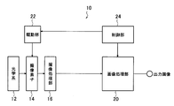
- FIG. 1 shows a schematic block diagram of the imaging apparatus 10 according to the present embodiment.
- the imaging device 10 includes an optical system 12, an imaging element 14, an imaging processing unit 16, an image processing unit 20, a driving unit 22, and a control unit 24.
- the optical system 12 includes, for example, a lens group including a plurality of optical lenses, an aperture adjustment mechanism, a zoom mechanism, an automatic focus adjustment mechanism, and the like.
- the image sensor 14 includes an image sensor including a plurality of photoelectric conversion elements arranged in a horizontal direction and a vertical direction, for example, a color filter disposed on an image sensor such as a CCD (Charge-Coupled Device) or a CMOS (Complementary Metal-Oxide Semiconductor). This is a so-called single-plate type imaging device having the above-described configuration.
- a CCD Charge-Coupled Device
- CMOS Complementary Metal-Oxide Semiconductor
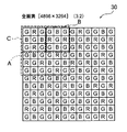
- FIG. 2 shows a part of the color filter 30 according to this embodiment.
- the number of pixels is (4896 ⁇ 3264) pixels as an example and the aspect ratio is 3: 2, but the number of pixels and the aspect ratio are not limited thereto.
- the color filter 30 includes a 3 ⁇ 3 pixel square array in which a first filter G (hereinafter referred to as a G filter) corresponding to G (green) that contributes most to obtain a luminance signal.
- a second filter R hereinafter referred to as an R filter
- R corresponding to R (red) is disposed on the center line in the horizontal direction of the square array, and B (blue).
- the first basic array pattern A Of the first array pattern A, the first basic array pattern A, and the filter G arranged in the center line in the vertical direction of the square array.
- the color filter 30 has the following features (1), (2), (3), (4), and (5).
- the color filter 30 shown in FIG. 2 includes a basic array pattern C composed of square array patterns corresponding to 6 ⁇ 6 pixels, and the basic array pattern C is repeatedly arranged in the horizontal direction and the vertical direction. That is, in this color filter array, R, G, and B color filters (R filter, G filter, and B filter) are arrayed with a predetermined periodicity.
- the synchronization (interpolation) processing also referred to as demosaic processing
- processing can be performed repeatedly according to the pattern.
- the color filter array of the reduced image after the thinning process can be the same as the color filter array before the thinning process, and a common processing circuit is provided. Can be used.
- the G filter corresponding to the color (G color in this embodiment) that contributes most to obtain the luminance signal corresponds to the horizontal, vertical, and diagonal lines of the color filter array. Is placed inside.
- G filters corresponding to luminance pixels are arranged in horizontal, vertical, and diagonal lines of the color filter array, improving the reproducibility of synchronization processing in the high frequency range regardless of the direction of high frequency. Can be made.
- the color filter 30 shown in FIG. 2 has an R filter and a B filter corresponding to two or more other colors (in this embodiment, R and B colors) other than the G color, And arranged in each vertical line.
- the R filter and B filter are arranged in the horizontal and vertical lines of the color filter array, the occurrence of color moire (false color) can be suppressed. Thereby, it is possible to prevent an optical low-pass filter for suppressing the occurrence of false colors from being arranged in the optical path from the incident surface of the optical system to the imaging surface. Even when an optical low-pass filter is applied, it is possible to apply a filter having a weak function of cutting a high-frequency component for preventing the occurrence of false colors, so that the resolution is not impaired.
- the basic array pattern C includes a 3 ⁇ 3 pixel first array pattern A surrounded by a broken line frame, and a 3 ⁇ 3 pixel second array pattern B surrounded by a dashed line frame.
- the arrangement is arranged alternately in the horizontal and vertical directions.
- G filters which are luminance pixels, are arranged at the four corners and the center, and are arranged on both diagonal lines.
- the B filter is arranged in the horizontal direction and the R filter is arranged in the vertical direction across the center G filter, while the second arrangement pattern B is arranged in the center G filter.
- the R filters are arranged in the horizontal direction, and the B filters are arranged in the vertical direction. That is, in the first arrangement pattern A and the second arrangement pattern B, the positional relationship between the R filter and the B filter is reversed, but the other arrangements are the same.
- the G filters at the four corners of the first array pattern A and the second array pattern B have the first array pattern A and the second array pattern B alternately in the horizontal and vertical directions as shown in FIG. Are arranged in a square array corresponding to 2 ⁇ 2 pixels.
- the color filter 30 shown in FIG. 2 includes a square array corresponding to 2 ⁇ 2 pixels made of a G filter.
- this color filter array it is possible to determine a direction having a high correlation among the horizontal direction, the vertical direction, and the diagonal direction by using the information of the G pixel having the minimum pixel interval.
- This direction discrimination result can be used for a process of interpolating from surrounding pixels (synchronization process).
- the basic arrangement pattern C of the color filter 30 shown in FIG. 2 is point-symmetric with respect to the center of the basic arrangement pattern C (the centers of the four G filters). Further, as shown in FIG. 2, the first array pattern A and the second array pattern B in the basic array pattern C are also point-symmetric with respect to the central G filter.
- the color filter arrangement of the first and third lines in the horizontal first to sixth lines is GRGGBG, and the color filter arrangement of the second line.
- the color filter array of the fourth and sixth lines is GBGGRG
- the color filter array of the fifth line is RGRBGB.
- the basic array pattern C in which the basic array pattern is point-symmetric is referred to as a basic array pattern for convenience.
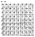
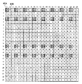
- the imaging element 14 Since the imaging device 10 performs so-called phase difference AF control, the imaging element 14 has phase detection pixels arranged in a predetermined pattern. On this phase difference detection pixel, as shown in FIG. 3, a light shielding part 40 including a light shielding film 40A for shielding the left half pixel in the horizontal direction and a light shielding film 40B for shielding the right half pixel in the horizontal direction. Is formed.
- the phase difference AF control the amount of phase shift is detected based on the pixel data of the phase difference detection pixel provided with the light shielding film 40A and the pixel data of the phase difference detection pixel provided with the light shielding film 40B. The focus position of the taking lens is adjusted based on the above.
- the light shielding unit 40 is provided with two sets of the first arrangement pattern A and the second arrangement pattern B that constitute the basic arrangement pattern C, and a G filter at the upper left corner.
- Each of the phase difference detection pixels is provided on each of the basic arrangement patterns C. That is, in the example of FIG. 3, the light shielding film 40A is arranged on the (6n + 1) th line in the vertical direction, and the light shielding film 40B is arranged on the (6n + 4) th line.
- the light-shielding portions 40 are provided for all the basic array patterns C.
- the present invention is not limited thereto, and may be provided only for the basic array patterns C in a predetermined region of a part of the image sensor. Good. The same applies to the following embodiments.
- the color filter 30 according to the present embodiment is provided on the phase difference detection pixel in which the light shielding unit 40 is provided with the G filters at the upper left corners of all the first array pattern A and the second array pattern B.
- the light shielding unit 40 is provided with the G filters at the upper left corners of all the first array pattern A and the second array pattern B.
- one pixel per three pixels and phase difference detection pixels are regularly arranged in both the vertical and horizontal directions. For this reason, since a relatively large number of normal pixels are arranged around the phase difference detection pixels, it is possible to improve the interpolation accuracy when interpolating the pixel data of the phase difference detection pixels from the pixel data of the normal pixels.
- the imaging processing unit 16 performs predetermined processing such as amplification processing, correlated double sampling processing, A / D conversion processing, and the like on the imaging signal output from the imaging device 14 and outputs it to the image processing unit 20 as pixel data. To do.
- the image processing unit 20 performs so-called synchronization processing on the pixel data output from the imaging processing unit 16. That is, for all pixels, pixel data of colors other than the corresponding color is interpolated from the pixel data of surrounding pixels to generate R, G, and B pixel data of all pixels. Then, so-called YC conversion processing is performed on the generated R, G, and B pixel data to generate luminance data Y and color difference data Cr and Cb. Then, a resizing process for resizing these signals to a size corresponding to the shooting mode is performed.
- the driving unit 22 performs reading driving of the imaging signal from the imaging device 14 in accordance with an instruction from the control unit 24.
- the control unit 24 controls the drive unit 22 and the image processing unit 20 according to the shooting mode and the like. Although details will be described later, the control unit 24 instructs the driving unit 22 to read out the imaging signal by a reading method according to the shooting mode, or instructs the image processing unit 20 to select an image according to the shooting mode. Or instructing it to perform processing.
- control unit 24 instructs the drive unit 22 to read out the image pickup signal using a thinning method according to the instructed shooting mode. To do.
- the shooting mode includes a still image mode for shooting a still image, and an HD movie that generates a relatively high resolution HD (high definition) movie data by thinning the captured image and records it on a recording medium such as a memory card (not shown).
- a moving image mode such as a through moving image mode (live view mode) that thins out a captured image and outputs a relatively low resolution through moving image to a display unit (not shown).
- processing shown in FIG. 4 is executed when an instruction is given to execute shooting according to the shooting mode.
- step 100 the drive unit 22 is instructed to read out pixel data by a thinning method corresponding to the shooting mode.
- the phase difference AF control is performed, and the other (6n + 2), (6n + 3), (6n + 5), and (6n + 6) th lines, that is, at least a part of the normal pixel lines are read out, Create data.
- the phase difference detection pixels are interpolated from the pixel data of the surrounding normal pixels.
- the present embodiment has a configuration in which one pixel per three pixels and phase difference detection pixels are regularly arranged in both the vertical and horizontal directions. For this reason, since a relatively large number of normal pixels are arranged around the phase difference detection pixels, it is possible to improve the interpolation accuracy when interpolating the pixel data of the phase difference detection pixels from the pixel data of the normal pixels.
- step 102 the image processing unit 20 is instructed to execute image processing (synchronization processing and YC conversion processing) and resizing processing according to the shooting mode.
- the control unit 24 can be configured by a computer including a CPU, ROM, RAM, nonvolatile ROM, and the like.
- the processing program for the above processing can be stored in advance in a nonvolatile ROM, for example, and can be read and executed by the CPU.
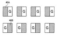
- FIGS. 3 and 5A an array line in which the light shielding film 40A is disposed along the horizontal direction and an array line in which the light shielding film 40B is disposed along the horizontal direction are provided.
- the arrangement lines alternately arranged in the horizontal direction in order may be arranged alternately in the vertical direction.
- FIG. 5 shows only the phase difference detection pixels.
- both the light shielding film 40A and the light shielding film 40B are arranged obliquely, so that, for example, when a subject including an oblique line is photographed, it is possible to focus accurately.
- FIG. 6 shows the arrangement of the light shielding films 40A and 40B according to the present embodiment. This embodiment is different from the first embodiment in the arrangement of the light shielding films 40A and 40B.
- the light shielding unit 40 is provided in each of two sets of the first array pattern A and the second array pattern B constituting the basic array pattern C, and the light shielding unit 40.
- the array lines in which the basic array pattern C in which the light shielding film 40 is disposed are arranged in the horizontal direction, and the array lines in which the basic array pattern C in which the light shielding film 40 is not disposed are disposed in the horizontal direction are alternately arranged in the vertical direction. Is arranged. That is, in the example of FIG. 6, the light shielding film 40A is disposed on the (12n + 1) th line in the vertical direction, and the light shielding film 40B is disposed on the (12n + 4) th line.
- the control unit 24 reads out the pixel data of the phase difference detection pixels on the line where the light shielding films 40A and 40B are arranged, performs phase difference AF control, and also performs the light shielding films 40A and 40B.
- pixel data of a normal pixel in which is not arranged for example, pixel data of the (12n + 7) th to (12n + 12) th lines is read to create moving image data.
- the pixel data of the phase difference detection pixel is used only for the phase difference AF control and is not used for creating the moving image data. Therefore, it is not necessary to interpolate from surrounding pixels.
- the moving image data is created from pixel data of normal pixels. Therefore, the processing speed of the phase difference AF control can be improved as compared with the case where the phase difference detection pixels are based on the creation of moving image data. In addition, the processing speed of moving image data creation can be improved as compared with the case where moving image data is generated by interpolation.
- FIG. 7 shows the arrangement of the light shielding films 40A and 40B according to the present embodiment. This embodiment is different from the first embodiment in the arrangement of the light shielding films 40A and 40B.
- the thinning drive is the same as in the second embodiment.
- the light shielding unit 40 includes a pair of first array patterns A and a second array pattern B that constitute the basic array pattern C, arranged in the vertical direction.
- An array line in which the basic array pattern C provided in the first array pattern A and the second array pattern B and in which the light shielding film 40 is disposed is disposed along the horizontal direction, and a base in which the light shielding film 40 is not disposed.
- the array lines in which the array pattern C is disposed along the horizontal direction are alternately disposed in the vertical direction. That is, in the example of FIG.
- the light shielding films 40A and 40B are disposed on the phase difference detection pixels at positions where the lines intersect.
- the number of normal pixels increases around the phase difference detection pixels, so that the interpolation accuracy can be improved and the image quality can be improved.
- FIG. 8 shows the arrangement of the light shielding films 40A and 40B according to the present embodiment. This embodiment is different from the first embodiment in the arrangement of the light shielding films 40A and 40B.
- the light shielding film 40 is provided on one side (left side) in the horizontal direction among the four corners of the set of the first array pattern A and the second array pattern B arranged in the horizontal direction. They are provided on the phase difference detection pixels at the two corners, and are arranged for all the basic array patterns C. That is, in the example of FIG. 8, the light shielding film 40A is disposed on the (6n + 1) th line in the vertical direction, and the light shielding film 40B is disposed on the (6n + 3) th line.
- the accuracy of AF control is better when the phase difference detection pixels are adjacent to each other or the phase difference detection pixels are arranged in the vertical direction.
- the accuracy of the phase difference AF control can be improved.
- FIG. 9 shows the arrangement of the light shielding films 40A and 40B according to the present embodiment. This embodiment is different from the first embodiment in the arrangement of the light shielding films 40A and 40B.
- the thinning drive is the same as in the second embodiment.
- the light-shielding portion 40 is located on one side (left side) in the horizontal direction among the four corners of the pair of first array pattern A and second array pattern B arranged in the horizontal direction.
- An array line that is provided on each of the phase difference detection pixels at the two corners and in which the basic array pattern C in which the light shielding film 40 is disposed is disposed along the horizontal direction, and a basic array in which the light shielding film 40 is not disposed.
- the array lines in which the patterns C are arranged along the horizontal direction are alternately arranged in the vertical direction. That is, in the example of FIG. 9, the light shielding film 40A is disposed on the (12n + 1) th line in the vertical direction, and the light shielding film 40B is disposed on the (12n + 3) th line.
- the control unit 24 reads out the pixel data of the phase difference detection pixels on the line where the light shielding films 40A and 40B are arranged, and performs phase difference AF control.
- the pixel data of the normal pixels where the light-shielding films 40A and 40B are not arranged, for example, the (12n + 7) th to (12n + 12) th lines are read to create moving image data.
- the pixel data of the phase difference detection pixel is used only for the phase difference AF control and is not used for creating the moving image data. Therefore, it is not necessary to interpolate from surrounding pixels.
- the moving image data is created from pixel data of normal pixels. Therefore, the processing speed of the phase difference AF control can be improved as compared with the case where the phase difference detection pixels are based on the creation of moving image data. In addition, the processing speed of moving image data creation can be improved as compared with the case where moving image data is generated by interpolation.
- FIG. 10 shows the arrangement of the light shielding films 40A and 40B according to the present embodiment. This embodiment is different from the first embodiment in the arrangement of the light shielding films 40A and 40B.
- the light shielding films 40A and 40B are disposed on the phase difference detection pixels at positions where the lines intersect.
- the image quality of the through video can be improved.
- the color filter array of the three primary colors of RGB has been described, but the type of color filter is not limited to this.
- the configuration in which the phase difference detection pixel is provided with the light shielding film 40A that shields the left half pixel in the horizontal direction or the light shielding film 40B that shields the right half pixel in the horizontal direction has been described.
- the light shielding region is not limited to this, and the light shielding film 40A shields a part of the phase difference detection pixel and transmits the other region, and the light shielding film 40B includes the phase difference detection pixel. As long as a part of the light is shielded and the region that is paired with the region through which the light shielding film 40A transmits is transmitted, it is sufficient.
- a phase difference detection pixel may be formed. That is, the imaging element is composed of a top microlens, an inner microlens, and a light receiving element having the same shape, and the first pixel D1 that receives a light beam that passes through the entire area of the photographing lens pupil and one half of the area of the photographing lens pupil.
- the top microlenses L2 and L3 having a smaller diameter than the top microlens L1 of the first pixel D1 are connected to the inner microlens. Each is shifted in a different direction with respect to the optical axis. In addition, the top microlens and the light receiving element are shifted from each other.
- the second pixel D2 and the third D3 can be formed as phase difference detection pixels. Even in such a configuration, the present invention is applicable. Furthermore, the form which does not provide an inner lens may be sufficient depending on the structure of an image pick-up element. Further, the configuration of the phase difference pixel is not limited to the above configuration, and can be replaced as long as the pupil division can be performed.
- Phase difference detection pixels have different characteristics, such as low sensitivity compared to normal pixels. Therefore, when using pixel data of phase difference detection pixels as image data for still images or moving images, phase difference detection pixels This pixel data needs to be corrected. Therefore, in the present embodiment, a method for correcting pixel data of phase difference detection pixels will be described.
- the average value correction is a method of averaging pixel values of normal pixels around the phase difference detection pixels and using this as pixel data of the phase difference detection pixels.
- the gain correction is a method of raising the pixel data of the phase difference detection pixel by multiplying the pixel data of the phase difference detection pixel by a predetermined gain corresponding to the level difference between the normal pixel and the phase difference detection pixel. It is.
- FIG. 14 shows the arrangement of G pixels in 4 ⁇ 4 pixels centered on the 2 ⁇ 2 G pixels in the center of the basic array pattern C.
- the center 2 ⁇ 2 G pixels are respectively G1, G2, G3, and G4 clockwise from the upper left
- the surrounding G pixels are respectively G5, G6, G7, and G8 clockwise from the upper left. .
- the G3 pixel in FIG. 14 is the phase difference detection pixel.
- the G2 or G3 pixel in FIG. 14 is the phase difference detection pixel.
- phase difference detection pixels are arranged as shown in FIG. 10, any of G1, G2, G3, and G4 pixels in FIG. 14 is the phase difference detection pixel.
- the average value of the pixel data of the surrounding normal pixels for example, the G2, G4, and G5 pixels, is used as the pixel data of the G1 pixel.
- the average value of the pixel data of each of the surrounding normal pixels, for example, G1, G3, and G6, is obtained as the pixel data of the G2 pixel.
- the average value of pixel data of the surrounding normal pixels for example, G2, G4, and G7, is obtained as pixel data of G3 pixels.
- G4 pixels which are phase difference detection pixels
- the average value of pixel data of the surrounding normal pixels for example, G1, G3, and G8, is obtained as pixel data of G4 pixels.
- the average value of the pixel data of the phase difference detection pixels is corrected based on the pixel data of the surrounding normal pixels.
- the gain correction and the average value correction may be properly used according to the content of the captured image.
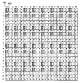
- FIG. 15 shows the arrangement of the light shielding films 40A and 40B according to the present embodiment. This embodiment is different from the first embodiment in the arrangement of the light shielding films 40A and 40B.
- a light shielding film 40A (first phase difference detection pixel) is disposed at the pixel position.
- the light shield film 40A is disposed.
- the light shielding film 40B (second phase difference detection pixel) at the pixel position corresponding to one corner (upper left corner in FIG. 15) of the four corners of the array pattern at the same position in the horizontal direction as the arranged pattern ) Is arranged.
- the control unit 24 except for the line where the light shielding films 40A and 40B are arranged, the normal pixel where the light shielding films 40A and 40B are not arranged, for example, the (2n + 2) th line. Pixel data is read to create moving image data. That is, moving image data is created by reading line image data of even-numbered lines in the vertical direction.
- both the light shielding film 40A and the light shielding film 40B are arranged on the odd-numbered lines in the vertical direction, the line image data of the even-numbered lines in the vertical direction is read to create moving image data. can do.
- the light shielding film 40A or the light shielding film 40B is arranged in any of 2 ⁇ 2 G pixels, and many G pixels that are normal pixels of the same color are arranged around the light shielding film 40A or the light shielding film 40B. Therefore, when generating image data using pixel data of phase difference detection pixels in still image shooting mode, etc., the interpolation accuracy when interpolating pixel data of phase difference detection pixels from pixel data of normal pixels is improved. Can be improved.
- the light shielding film 40A is disposed at the lower corner in the vertical direction among the four corners of the first array pattern A, and the light shielding film 40B paired with the light shielding film 40A is disposed at the four corners of the first array pattern A. Since the light shielding film 40B is disposed at the lower side in the vertical direction among the four corners of the first array pattern A, the light shielding film 40B is disposed at the upper corner in the vertical direction. In comparison, since the distance in the vertical direction between the light shielding film 40A and the light shielding film 40B that form a pair is reduced, the AF accuracy by the phase difference detection pixels can be improved.
- the present invention is not limited to this.
- the light shielding film 40A may be disposed on the (12n + 1) th line in the vertical direction, and the light shielding film 40B may be disposed on the (12n + 7) th line.
- the light shielding film 40A may be disposed on the (12n + 3) th line in the vertical direction, and the light shielding film 40B may be disposed on the (12n + 9) th line.
- Imaging device 12 Optical system 14 Imaging element 16 Imaging processing part 20 Image processing part 22 Drive part 24 Control part 30 Color filter
Landscapes
- Engineering & Computer Science (AREA)
- Multimedia (AREA)
- Signal Processing (AREA)
- Physics & Mathematics (AREA)
- Spectroscopy & Molecular Physics (AREA)
- Color Television Image Signal Generators (AREA)
- Focusing (AREA)
- Automatic Focus Adjustment (AREA)
- Studio Devices (AREA)
Abstract
Priority Applications (4)
| Application Number | Priority Date | Filing Date | Title |
|---|---|---|---|
| JP2013505921A JP5490312B2 (ja) | 2011-03-24 | 2012-03-14 | カラー撮像素子、撮像装置、及び撮像装置の制御プログラム |
| CN201280014651.5A CN103444184B (zh) | 2011-03-24 | 2012-03-14 | 彩色摄像元件及摄像装置 |
| EP12761264.6A EP2690875A4 (fr) | 2011-03-24 | 2012-03-14 | Élément d'imagerie en couleur, dispositif d'imagerie, et programme de commande de dispositif d'imagerie |
| US14/034,004 US8736743B2 (en) | 2011-03-24 | 2013-09-23 | Color imaging element, imaging device, and storage medium storing a control program for imaging device |
Applications Claiming Priority (6)
| Application Number | Priority Date | Filing Date | Title |
|---|---|---|---|
| JP2011-066631 | 2011-03-24 | ||
| JP2011066631 | 2011-03-24 | ||
| JP2011163311 | 2011-07-26 | ||
| JP2011-163311 | 2011-07-26 | ||
| JP2011-289042 | 2011-12-28 | ||
| JP2011289042 | 2011-12-28 |
Related Child Applications (1)
| Application Number | Title | Priority Date | Filing Date |
|---|---|---|---|
| US14/034,004 Continuation US8736743B2 (en) | 2011-03-24 | 2013-09-23 | Color imaging element, imaging device, and storage medium storing a control program for imaging device |
Publications (1)
| Publication Number | Publication Date |
|---|---|
| WO2012128153A1 true WO2012128153A1 (fr) | 2012-09-27 |
Family
ID=46879304
Family Applications (1)
| Application Number | Title | Priority Date | Filing Date |
|---|---|---|---|
| PCT/JP2012/056594 Ceased WO2012128153A1 (fr) | 2011-03-24 | 2012-03-14 | Élément d'imagerie en couleur, dispositif d'imagerie, et programme de commande de dispositif d'imagerie |
Country Status (5)
| Country | Link |
|---|---|
| US (1) | US8736743B2 (fr) |
| EP (1) | EP2690875A4 (fr) |
| JP (1) | JP5490312B2 (fr) |
| CN (1) | CN103444184B (fr) |
| WO (1) | WO2012128153A1 (fr) |
Cited By (1)
| Publication number | Priority date | Publication date | Assignee | Title |
|---|---|---|---|---|
| KR20160016142A (ko) * | 2014-08-04 | 2016-02-15 | 엘지이노텍 주식회사 | 이미지 센서 및 이를 포함하는 촬상 장치 |
Families Citing this family (9)
| Publication number | Priority date | Publication date | Assignee | Title |
|---|---|---|---|---|
| WO2012127701A1 (fr) * | 2011-03-24 | 2012-09-27 | 富士フイルム株式会社 | Élément d'imagerie en couleur, dispositif d'imagerie, et programme d'imagerie |
| JP5526287B2 (ja) * | 2011-04-28 | 2014-06-18 | 富士フイルム株式会社 | 撮像装置及び撮像方法 |
| JP6405243B2 (ja) * | 2014-03-26 | 2018-10-17 | キヤノン株式会社 | 焦点検出装置及びその制御方法 |
| JP6364259B2 (ja) * | 2014-07-02 | 2018-07-25 | オリンパス株式会社 | 撮像装置、画像処理方法、及び画像処理プログラム |
| JP2018046394A (ja) * | 2016-09-14 | 2018-03-22 | オリンパス株式会社 | 撮像素子、撮像装置 |
| CN109788199B (zh) * | 2019-01-30 | 2021-02-05 | 上海创功通讯技术有限公司 | 一种适用于具有双摄像头终端的对焦方法 |
| CN110235433A (zh) * | 2019-04-30 | 2019-09-13 | 深圳市汇顶科技股份有限公司 | 像素阵列排布方法、像素阵列、图像传感器和终端 |
| CN112866545B (zh) * | 2019-11-12 | 2022-11-15 | Oppo广东移动通信有限公司 | 对焦控制方法和装置、电子设备、计算机可读存储介质 |
| CN115696040B (zh) * | 2022-10-20 | 2025-10-10 | 西安立讯信息技术有限公司 | 对焦方法及装置、电子设备、计算机可读存储介质 |
Citations (9)
| Publication number | Priority date | Publication date | Assignee | Title |
|---|---|---|---|---|
| JP2000156823A (ja) | 1998-08-20 | 2000-06-06 | Canon Inc | 固体撮像装置及びその制御方法及び撮像装置及び光電変換セルの基本配列及び記憶媒体 |
| JP2007155929A (ja) | 2005-12-01 | 2007-06-21 | Nikon Corp | 固体撮像素子及びこれを用いた撮像装置 |
| JP2008312073A (ja) | 2007-06-16 | 2008-12-25 | Nikon Corp | 固体撮像素子及びこれを用いた撮像装置 |
| JP2009089144A (ja) | 2007-10-01 | 2009-04-23 | Nikon Corp | 電子カメラ |
| JP2009105682A (ja) | 2007-10-23 | 2009-05-14 | Nikon Corp | 撮像素子および撮像装置 |
| JP2009227338A (ja) | 2008-02-28 | 2009-10-08 | Chugoku Electric Power Co Inc:The | 作業服類の保管袋及びこれを用いた保管方法 |
| JP2010066494A (ja) | 2008-09-10 | 2010-03-25 | Olympus Corp | 固体撮像素子及びデジタルカメラ |
| JP2010512048A (ja) * | 2006-11-30 | 2010-04-15 | イーストマン コダック カンパニー | 低解像度画像の生成 |
| JP2010154493A (ja) * | 2008-11-21 | 2010-07-08 | Sony Corp | 撮像装置 |
Family Cites Families (17)
| Publication number | Priority date | Publication date | Assignee | Title |
|---|---|---|---|---|
| JPS58219889A (ja) * | 1982-06-14 | 1983-12-21 | Shoichi Tanaka | 固体撮像装置 |
| JPH0823543A (ja) | 1994-07-07 | 1996-01-23 | Canon Inc | 撮像装置 |
| JPH0823542A (ja) | 1994-07-11 | 1996-01-23 | Canon Inc | 撮像装置 |
| EP0930789B1 (fr) | 1998-01-20 | 2005-03-23 | Hewlett-Packard Company, A Delaware Corporation | Appareil de prise de vues en couleurs |
| JP4098438B2 (ja) | 1999-04-15 | 2008-06-11 | オリンパス株式会社 | カラー撮像素子及びカラー撮像装置 |
| JP4088959B2 (ja) | 2001-01-09 | 2008-05-21 | ソニー株式会社 | 画像処理装置および方法、並びに記録媒体 |
| JP4019417B2 (ja) | 2003-01-14 | 2007-12-12 | ソニー株式会社 | 画像処理装置および方法、記録媒体、並びにプログラム |
| JP2004266369A (ja) | 2003-02-21 | 2004-09-24 | Sony Corp | 固体撮像装置およびその駆動方法 |
| JP4385282B2 (ja) | 2003-10-31 | 2009-12-16 | ソニー株式会社 | 画像処理装置および画像処理方法 |
| US7821553B2 (en) | 2005-12-30 | 2010-10-26 | International Business Machines Corporation | Pixel array, imaging sensor including the pixel array and digital camera including the imaging sensor |
| JP4662883B2 (ja) | 2006-05-15 | 2011-03-30 | 富士フイルム株式会社 | 二次元カラー固体撮像素子 |
| US7701496B2 (en) | 2006-12-22 | 2010-04-20 | Xerox Corporation | Color filter pattern for color filter arrays including a demosaicking algorithm |
| JP5082528B2 (ja) | 2007-03-23 | 2012-11-28 | ソニー株式会社 | 固体撮像装置及び撮像装置 |
| WO2009020031A1 (fr) * | 2007-08-06 | 2009-02-12 | Canon Kabushiki Kaisha | Appareil de détection d'image |
| EP3328048B1 (fr) | 2008-05-20 | 2021-04-21 | FotoNation Limited | Capture et traitement d'images au moyen d'un réseau de caméras monolithiques avec des imageurs hétérogènes |
| JP5149143B2 (ja) | 2008-12-24 | 2013-02-20 | シャープ株式会社 | 固体撮像素子およびその製造方法、電子情報機器 |
| JP5471117B2 (ja) * | 2009-07-24 | 2014-04-16 | ソニー株式会社 | 固体撮像装置とその製造方法並びにカメラ |
-
2012
- 2012-03-14 JP JP2013505921A patent/JP5490312B2/ja not_active Expired - Fee Related
- 2012-03-14 EP EP12761264.6A patent/EP2690875A4/fr not_active Withdrawn
- 2012-03-14 WO PCT/JP2012/056594 patent/WO2012128153A1/fr not_active Ceased
- 2012-03-14 CN CN201280014651.5A patent/CN103444184B/zh not_active Expired - Fee Related
-
2013
- 2013-09-23 US US14/034,004 patent/US8736743B2/en not_active Expired - Fee Related
Patent Citations (10)
| Publication number | Priority date | Publication date | Assignee | Title |
|---|---|---|---|---|
| JP2000156823A (ja) | 1998-08-20 | 2000-06-06 | Canon Inc | 固体撮像装置及びその制御方法及び撮像装置及び光電変換セルの基本配列及び記憶媒体 |
| JP3592147B2 (ja) | 1998-08-20 | 2004-11-24 | キヤノン株式会社 | 固体撮像装置 |
| JP2007155929A (ja) | 2005-12-01 | 2007-06-21 | Nikon Corp | 固体撮像素子及びこれを用いた撮像装置 |
| JP2010512048A (ja) * | 2006-11-30 | 2010-04-15 | イーストマン コダック カンパニー | 低解像度画像の生成 |
| JP2008312073A (ja) | 2007-06-16 | 2008-12-25 | Nikon Corp | 固体撮像素子及びこれを用いた撮像装置 |
| JP2009089144A (ja) | 2007-10-01 | 2009-04-23 | Nikon Corp | 電子カメラ |
| JP2009105682A (ja) | 2007-10-23 | 2009-05-14 | Nikon Corp | 撮像素子および撮像装置 |
| JP2009227338A (ja) | 2008-02-28 | 2009-10-08 | Chugoku Electric Power Co Inc:The | 作業服類の保管袋及びこれを用いた保管方法 |
| JP2010066494A (ja) | 2008-09-10 | 2010-03-25 | Olympus Corp | 固体撮像素子及びデジタルカメラ |
| JP2010154493A (ja) * | 2008-11-21 | 2010-07-08 | Sony Corp | 撮像装置 |
Non-Patent Citations (1)
| Title |
|---|
| See also references of EP2690875A4 |
Cited By (3)
| Publication number | Priority date | Publication date | Assignee | Title |
|---|---|---|---|---|
| KR20160016142A (ko) * | 2014-08-04 | 2016-02-15 | 엘지이노텍 주식회사 | 이미지 센서 및 이를 포함하는 촬상 장치 |
| US9906744B2 (en) | 2014-08-04 | 2018-02-27 | Lg Innotek Co., Ltd. | Image sensor having phase difference detection pixels for focus detection, and image pick-up apparatus including the image sensor |
| KR102346622B1 (ko) * | 2014-08-04 | 2022-01-04 | 엘지이노텍 주식회사 | 이미지 센서 및 이를 포함하는 촬상 장치 |
Also Published As
| Publication number | Publication date |
|---|---|
| US20140022422A1 (en) | 2014-01-23 |
| US8736743B2 (en) | 2014-05-27 |
| EP2690875A1 (fr) | 2014-01-29 |
| JP5490312B2 (ja) | 2014-05-14 |
| JPWO2012128153A1 (ja) | 2014-07-24 |
| CN103444184B (zh) | 2014-10-29 |
| CN103444184A (zh) | 2013-12-11 |
| EP2690875A4 (fr) | 2014-11-05 |
Similar Documents
| Publication | Publication Date | Title |
|---|---|---|
| JP5490313B2 (ja) | カラー撮像素子、撮像装置、及び撮像装置の制御プログラム | |
| JP5490312B2 (ja) | カラー撮像素子、撮像装置、及び撮像装置の制御プログラム | |
| JP5547338B2 (ja) | カラー撮像素子、撮像装置、及び撮像プログラム | |
| JP5539585B2 (ja) | カラー撮像素子、撮像装置、及び撮像プログラム | |
| JP5539584B2 (ja) | カラー撮像素子、撮像装置、及び撮像プログラム | |
| JP5680797B2 (ja) | 撮像装置、画像処理装置、及び画像処理方法 | |
| JP5539583B2 (ja) | カラー撮像素子、撮像装置、及び撮像プログラム | |
| JP5624227B2 (ja) | 撮像装置、撮像装置の制御方法、及び制御プログラム | |
| JP2015161727A (ja) | 撮像素子および撮像装置 |
Legal Events
| Date | Code | Title | Description |
|---|---|---|---|
| 121 | Ep: the epo has been informed by wipo that ep was designated in this application |
Ref document number: 12761264 Country of ref document: EP Kind code of ref document: A1 |
|
| ENP | Entry into the national phase |
Ref document number: 2013505921 Country of ref document: JP Kind code of ref document: A |
|
| NENP | Non-entry into the national phase |
Ref country code: DE |
|
| REEP | Request for entry into the european phase |
Ref document number: 2012761264 Country of ref document: EP |
|
| WWE | Wipo information: entry into national phase |
Ref document number: 2012761264 Country of ref document: EP |