WO2012131833A1 - Film d'absorption de lumière, son procédé de production, et collecteur thermique solaire utilisant un tel film - Google Patents
Film d'absorption de lumière, son procédé de production, et collecteur thermique solaire utilisant un tel film Download PDFInfo
- Publication number
- WO2012131833A1 WO2012131833A1 PCT/JP2011/007196 JP2011007196W WO2012131833A1 WO 2012131833 A1 WO2012131833 A1 WO 2012131833A1 JP 2011007196 W JP2011007196 W JP 2011007196W WO 2012131833 A1 WO2012131833 A1 WO 2012131833A1
- Authority
- WO
- WIPO (PCT)
- Prior art keywords
- light
- light absorption
- absorption film
- titanium oxide
- carbon nanotubes
- Prior art date
- Legal status (The legal status is an assumption and is not a legal conclusion. Google has not performed a legal analysis and makes no representation as to the accuracy of the status listed.)
- Ceased
Links
Images






Classifications
-
- F—MECHANICAL ENGINEERING; LIGHTING; HEATING; WEAPONS; BLASTING
- F24—HEATING; RANGES; VENTILATING
- F24S—SOLAR HEAT COLLECTORS; SOLAR HEAT SYSTEMS
- F24S70/00—Details of absorbing elements
- F24S70/20—Details of absorbing elements characterised by absorbing coatings; characterised by surface treatment for increasing absorption
-
- F—MECHANICAL ENGINEERING; LIGHTING; HEATING; WEAPONS; BLASTING
- F24—HEATING; RANGES; VENTILATING
- F24S—SOLAR HEAT COLLECTORS; SOLAR HEAT SYSTEMS
- F24S70/00—Details of absorbing elements
- F24S70/20—Details of absorbing elements characterised by absorbing coatings; characterised by surface treatment for increasing absorption
- F24S70/225—Details of absorbing elements characterised by absorbing coatings; characterised by surface treatment for increasing absorption for spectrally selective absorption
-
- F—MECHANICAL ENGINEERING; LIGHTING; HEATING; WEAPONS; BLASTING
- F24—HEATING; RANGES; VENTILATING
- F24S—SOLAR HEAT COLLECTORS; SOLAR HEAT SYSTEMS
- F24S80/00—Details, accessories or component parts of solar heat collectors not provided for in groups F24S10/00-F24S70/00
- F24S2080/01—Selection of particular materials
- F24S2080/014—Carbone, e.g. graphite
-
- Y—GENERAL TAGGING OF NEW TECHNOLOGICAL DEVELOPMENTS; GENERAL TAGGING OF CROSS-SECTIONAL TECHNOLOGIES SPANNING OVER SEVERAL SECTIONS OF THE IPC; TECHNICAL SUBJECTS COVERED BY FORMER USPC CROSS-REFERENCE ART COLLECTIONS [XRACs] AND DIGESTS
- Y02—TECHNOLOGIES OR APPLICATIONS FOR MITIGATION OR ADAPTATION AGAINST CLIMATE CHANGE
- Y02E—REDUCTION OF GREENHOUSE GAS [GHG] EMISSIONS, RELATED TO ENERGY GENERATION, TRANSMISSION OR DISTRIBUTION
- Y02E10/00—Energy generation through renewable energy sources
- Y02E10/40—Solar thermal energy, e.g. solar towers
Definitions
- the present invention relates to a light-absorbing film, a manufacturing method thereof, and a solar heat collector using the same.
- a film containing chromium nitride is used as a light absorbing film used in a solar heat collector.
- chromium nitride is concerned with a large environmental load. Therefore, a titanium oxynitride thin film having a property of absorbing visible light has been proposed (see, for example, Patent Document 1). Further, it has been disclosed that the visible light absorption rate is improved by adding carbon to titanium oxynitride (see, for example, Patent Document 2).
- JP-T 9-507095 (Claims etc.)
- JP 2006-1820 A (Claims etc.)
- titanium oxynitride can absorb visible light.
- the addition of carbon in addition to the absorption of visible light by titanium oxynitride, the addition of carbon can improve the visible light absorption rate and infrared light radiation. However, it is desired to collect heat efficiently by further improving the light absorption rate of the light absorption film.
- the present invention has been made in response to such a demand, and an object thereof is to provide a light absorption film having a high light absorption rate, a method for producing the same, and a solar heat collector using the light absorption film.
- the present inventors have conducted intensive research. As a result, a light absorption film containing 100 parts by weight of titanium oxide and 2 to 10 parts by weight of carbon nanotubes is obtained, which is higher than the conventional product. It has been found that light absorption can be achieved.
- the present invention is a light absorption film containing 100 parts by weight of titanium oxide and 2 to 10 parts by weight of carbon nanotubes.
- the carbon nanotubes can be contained more on the back side than on the side that is irradiated with light.
- the light absorption film is formed in a three-dimensional network shape and a plurality of holes are formed.
- the light absorption film preferably has a light irradiation surface having a surface area of 3 times or more of the projected area.
- Another embodiment of the present invention is a method for producing a light-absorbing film containing 100 parts by weight of titanium oxide and 2 to 10 parts by weight of carbon nanotubes, wherein the carbon nanotubes are mixed in a solvent. And a coating step of coating a substrate with a titanium oxide precursor solution for producing titanium oxide and a solvent mixed with carbon nanotubes and heating the substrate.
- the mixing step may include a step of applying a pressure to the solvent mixed with the carbon nanotubes and causing the injected solvents to collide with each other to change the flow direction.
- the application step is applied to the heated substrate by spraying.
- Another aspect of the present invention is a solar collector including a light absorbing film containing 100 parts by weight of titanium oxide and 2 to 10 parts by weight of carbon nanotubes, and a substrate supporting the light absorbing film.
- a light absorption film having a high light absorption rate and a solar heat collector using the same can be provided.
- step S103 It is a flowchart which shows the flow of the manufacturing method of the light absorption film which concerns on this Embodiment. It is the schematic explaining the spraying method in step S103.
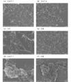
- A is an SEM photograph showing a mixed state of a 0.5 wt% carbon nanotube (VGCF-X) mixed solution.
- B is a SEM photograph showing a mixed state of a 0.5 wt% carbon nanotube (Arkema) mixed solution.
- C is an SEM photograph showing a mixed state of a 0.5 wt% carbon fiber (VGCF) mixed solution.
- D is an SEM photograph showing a mixed state of a 0.5 wt% ketjen black mixed solution.
- (E) is a SEM photograph showing a state where the mixed solution of FIG. 3 (A) is not dispersed.
- (E) is a SEM photograph showing a state in which the mixed solution of FIG. (A) is a photograph showing the appearance of the light-absorbing film obtained under the conditions of Example 1.
- (B) is a photograph showing the appearance of the light-absorbing film obtained under the conditions of Example 2.
- (C) is a photograph showing the appearance of the light absorption film obtained under the conditions of Example 3.
- (D) is a photograph showing the appearance of the light-absorbing film obtained under the conditions of Example 4.
- (E) is a photograph showing the appearance of the light-absorbing film obtained under the conditions of Comparative Example 1.
- (F) is a photograph showing the appearance of a state in which light is applied to the light absorption film obtained under the conditions of Comparative Example 2.
- (G) is a photograph showing the appearance when the light absorbing film of FIG. 4 (F) is viewed with light extinguished.
- (H) is a photograph showing the appearance of the light absorption film of Comparative Example 3.
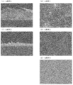
- (A) is the SEM photograph which observed the light absorption film obtained on the conditions of Example 1 from the light irradiation surface side.
- (B) is the SEM photograph which observed the light absorption film obtained on the conditions of Example 2 from the light irradiation surface side.
- (C) is the SEM photograph of the cross section of the light absorption film obtained on the conditions of Example 2.
- FIG. (D) is the SEM photograph which observed the light absorption film obtained on the conditions of Example 3 from the light irradiation surface side.
- (E) is the SEM photograph of the cross section of the light absorption film obtained on the conditions of Example 3.
- FIG. (F) is the SEM photograph which observed the light absorption film obtained on the conditions of Example 4 from the light irradiation surface side.
- (A) is the SEM photograph of the cross section of the light absorption film obtained on the conditions of the comparative example 1.
- FIG. (B) is an SEM photograph of the light absorbing film in FIG. 6 (A) observed from the light irradiation surface side.
- (C) is the SEM photograph of the cross section of the light absorption film obtained on the conditions of the comparative example 2.
- (D) is the SEM photograph which observed the light absorption film of FIG.6 (C) from the light irradiation surface side.
- (E) is the SEM photograph which observed the light absorption film of the comparative example 3 from the light irradiation surface side.
- (A) is the photograph which observed the light absorption film obtained on the conditions of Example 1 with the laser microscope from the light irradiation surface side.
- (B) is the photograph which observed the light absorption film obtained on the conditions of Example 2 with the laser microscope from the light irradiation surface side.
- (C) It is the photograph which observed the light absorption film obtained on the conditions of Example 3 with the laser microscope from the light irradiation surface side.
- (D) is the photograph which observed the light absorption film obtained on the conditions of Example 4 with the laser microscope from the light irradiation surface side.
- (A) is the photograph which observed the light absorption film obtained on the conditions of the comparative example 1 with the laser microscope from the light irradiation surface side.
- (B) is the photograph which observed the light absorption film obtained on the conditions of the comparative example 2 with the laser microscope from the light irradiation surface side.
- (C) It is the photograph which observed the light absorption film obtained on the conditions of the comparative example 3 with the laser microscope from the light irradiation surface side.
- (D) is the photograph which observed the light absorption film obtained on the conditions of the comparative example 4 with the laser microscope from the light irradiation surface side.
- 6 is an XRD chart of a light absorption film obtained under the conditions of Examples 2, 3, 6 and Comparative Examples 2, 4.
- 4 is a graph showing the diffuse reflectance of light diffused light on the vertical axis and the wavelength of light irradiated on the horizontal axis for the light absorbing films obtained under the conditions of Example 2, Comparative Example 1 and Comparative Example 2.
- 4 is a graph showing the diffuse reflectance of diffused light on the vertical axis and the wavelength of light irradiated on the horizontal axis for the light absorbing films obtained under the conditions of Examples 1 to 4 and Comparative Example 3.
- FIG. 9 is a graph showing the diffuse reflectance of diffused light on the vertical axis and the wavelength of irradiated light on the horizontal axis for the light absorbing films obtained under the conditions of Examples 6 to 8.
- 6 is an XRD chart of a light absorption film obtained under the conditions of Examples 7 and 8.
- FIG. (A) is the photograph which observed the light absorption film obtained on the conditions of Example 7 with the laser microscope from the light irradiation surface side.
- (B) is the photograph which observed the light absorption film obtained on the conditions of Example 8 with the laser microscope from the light irradiation surface side.
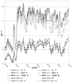
- the temperature change of the front and back surfaces of the light absorption film when each light absorption film obtained under the conditions of Example 2 and Comparative Examples 1 to 3 was irradiated with a xenon lamp was measured. It is a graph which shows irradiation time on an axis
- the temperature change of the front and back surfaces of the light absorption film when each light absorption film obtained under the conditions of Examples 1 to 3, Comparative Example 3 and Comparative Example 5 was irradiated with a xenon lamp was measured. It is a graph which shows irradiation temperature on the temperature and horizontal axis of this.
- the light absorbing film according to the present embodiment mainly contains titanium oxide and carbon nanotubes. Hereinafter, each of titanium oxide and carbon nanotube will be described.
- Titanium oxide that can be used in this embodiment is made from a titanium oxide precursor that can be thermally decomposed in an oxidizing atmosphere into titanium oxide.
- a titanium oxide precursor As such a titanium oxide precursor, an organic titanium compound and an inorganic titanium compound exist.
- organic titanium compound examples include tetraisopropoxy titanium, tetrabutoxy titanium, tetrakis (2-ethylhexyloxy) titanium, tetrastearyloxy titanium, diisopropoxy titanium bis (acetylacetonato), dinormal butoxy bis (triethanolaminato) Titanium, Titanium stearate, Titanium isopropoxyoctylene glycolate, Tetraisopropoxytitanium polymer, Tetranormal butoxytitanium polymer, Dihydroxybis (lactato) titanium, Propanedioxytitanium bis (ethylacetoacetate), Oxotitanium bis ( Monoammonium oxalate), tri-normal butoxy titanium monostearate, diisopropoxy titanium di Teareto, dihydroxy bis (lactato) titanium ammonium salts, and tetra - methoxy titanium, and the like.
- organic titanium compounds are used alone or in combination of two or more compounds.
- organic titanium compounds diisopropoxytitanium bis (acetylacetonato), tetranormalbutoxytitanium, tetraisopropoxytitanium, dinormalbutoxybis (triethanolaminato) titanium, and titanium isopropoxyoctylene glycolate Those consisting of one or more selected from the above can be preferably used from the viewpoints of storage stability of the material, selectivity of the solvent, the relationship between the thermal decomposition temperature and the crystallization temperature, and adhesion to the substrate.
- examples of the inorganic titanium compound include titanium chloride (TiCl 4 ). Note that an inorganic titanium compound and an organic titanium compound may be mixed and used.
- the titanium oxide precursor may be used as it is, or as a dispersion such as a solution or a colloidal solution, an emulsion or a suspension using a solvent or a dispersion medium.
- a dispersion such as a solution or a colloidal solution, an emulsion or a suspension using a solvent or a dispersion medium.
- a solvent or dispersion medium for using the titanium oxide precursor as a solution or dispersion alcohols such as ethanol, methanol, propanol, and butanol, hexane, toluene, chlorobenzene, methyl chloride, or perchloroethylene are preferably used. it can. Further, the solvent and the dispersion medium may contain a small amount of water. However, it is preferable to use an organic solvent having a somewhat high boiling point so that when the solution or dispersion of the titanium oxide precursor is sprayed, the solvent or dispersion medium does not volatilize before reaching the substrate. In addition, it is more preferable to use an organic solvent having a low viscosity because it can be easily discharged by spraying.
- the dissolution concentration or dispersion concentration of the titanium compound in the solvent or dispersion medium can be appropriately selected from the ease of application to the substrate, the thickness of the light absorption film to be formed, the crystallization state of titanium oxide, and the like.
- titanium compound in the case of the above-described titanium compound as a liquid, or as a solution or dispersion, while in the case of a solid, it is oxidized as a powder or as a solution or dispersion on a substrate heated to a heat decomposable temperature. Titanium oxide is produced
- the dissolution concentration or dispersion concentration of the titanium compound in the solvent or dispersion medium can be appropriately selected from the ease of application to the substrate, the thickness of the light absorption film to be formed, the crystallization state, and the like.
- the titanium oxide precursor is prepared to contain, for example, 0.2 to 1.0 mol / l titanium.
- titanium oxide When the titanium oxide precursor is applied as it is or as a solution or dispersion on a substrate heated to a temperature capable of being thermally decomposed in an oxidizing atmosphere, titanium oxide is generated.
- the temperature of the substrate is preferably 400 to 600 ° C., for example, and can be appropriately selected according to the decomposability of the titanium oxide precursor. Further, the crystallinity of the generated titanium oxide can be controlled by the temperature of the substrate.
- the oxidizing atmosphere it is only necessary that oxygen for generating titanium oxide by thermal decomposition exists in the air.
- the carbon nanotube as a carbon material that can be used in this embodiment may be a single-wall type, a double-wall type, or a multilayer type, or a mixture of two or more types.
- Carbon nanotubes having a diameter of 1 to 50 nm and a length of 20 to 500 nm can be preferably used. Among them, it is more preferable to use carbon nanotubes having a diameter of 10 to 15 nm.
- the carbon nanotubes are mixed with the titanium oxide precursor solution and sprayed onto the substrate together with the titanium oxide precursor solution.
- dispersion medium for dispersing the carbon nanotubes it is more preferable to mix the carbon nanotubes with the dispersion medium before mixing the carbon nanotubes with the titanium oxide precursor solution.
- the dispersion medium for dispersing the carbon nanotubes the same or different solvent or dispersion medium for dissolving or dispersing the titanium oxide precursor can be used.
- Carbon nanotubes are preferably mixed in an amount of 2 to 10 parts by weight, more preferably 2.5 to 5 parts by weight, based on 100 parts by weight of titanium oxide.
- the light absorbing film contains a carbon material of 2 parts by weight or more, and further 2.5 parts by weight or more with respect to 100 parts by weight of titanium oxide, the light absorption rate of the light absorbing film can be improved.
- the light absorption film contains carbon nanotubes of 10 parts by weight or less, and further 5 parts by weight or less with respect to 100 parts by weight of titanium oxide, the adhesion of the light absorption film to the substrate can be improved.
- the light absorption film preferably contains carbon nanotubes at a higher density on the substrate side (hereinafter referred to as “back side”) than on the light irradiation surface side (hereinafter referred to as “front side”).
- back side the substrate side
- front side the light irradiation surface side
- the carbon nanotubes are less likely to be detached from the light absorption film.
- the back side contains more carbon nanotubes than the front side, when the light absorption film receives light and converts light into heat, the heat is actively conducted from the front side to the back side.
- the carbon nanotube can function as a heat conduction path.
- the light absorption film having the above composition is mainly composed of titanium oxide and carbon, the environmental load is small.
- the light absorbing film having the above composition is formed in a tree shape or a three-dimensional network shape, and a plurality of pores are formed. With this structure, the light absorption rate of the light absorption film can be improved. This is because such a structure can increase the light-receiving area of the light absorption film.
- the light absorption film having such a structure can receive light incident from various directions and reflected light from the pores. In addition, the light receiving area of the light absorption film is increased by the pores, and the light irradiated to the light absorption film can reach the back of the light absorption film without regular reflection. It becomes easy to convey.
- a light absorption film using carbon nanotubes as a carbon material has a dense three-dimensional network structure.
- the surface area of the light absorbing surface of the light absorbing film is 3 times or more, preferably 7 times or more the projected area. Further, the light absorption surface of the light absorption film preferably has an arithmetic average roughness (Ra) of 1.0 or more, and preferably has a maximum height (Rz) of 15 or more.
- the “projection area” is an area of a certain measurement region (microscope field of view) viewed from a direction perpendicular to the surface of the substrate (a thickness direction of the substrate plate). “The surface area is at least 3 times the projected area” means that the actual surface area in the measurement region is at least 3 times the projected area of the measurement region. As the surface area relative to the projected area, Ra and Rz, values measured using a scanning confocal laser microscope can be used.
- FIG. 1 is a flowchart showing a flow of a method for manufacturing a light absorption film according to the present embodiment.
- step S101 mixing step
- the carbon nanotube mixed solution may be dispersed in the dispersion medium by applying vibration to the carbon nanotube mixed solution from the outside, adding a dispersing agent, or stirring the carbon nanotube mixed solution. .
- Carbon nanotubes tend to agglomerate when gathered by interparticle forces such as van der Waals forces and Coulomb forces.
- a pressure applying device that applies pressure to the dispersion medium, a plurality of introduction channels that introduce the dispersion medium pressurized by the pressure applying device, and an introduction flow
- the carbon nanotubes are dispersed in the dispersion medium by causing the dispersion medium containing the carbon nanotubes to collide and changing the flow direction. Is preferred.
- the carbon nanotube dispersion solution supplied to such an apparatus increases the collision force between the carbon nanotubes and maintains the viscosity of the solution, so that the carbon nanotubes are 0.001% to 30% with respect to the total weight of the solution. Is preferred.
- the carbon nanotube dispersion solution is pressurized to 100 MPa or more, preferably 100 to 200 MPa by a pressure applying device. When the carbon nanotube dispersion solution collides in such a pressurized state, the carbon nanotubes are easily broken and dispersed. In such a method, turbulent flow, high-speed flow, ultrasonic waves, shock waves, cavitation, or the like occurs, so that the carbon nanotubes can be dispersed in the dispersion medium.
- the light absorption film produced using the carbon nanotube mixed solution subjected to the dispersion treatment as described above has a high surface area in addition to high adhesion to the substrate as compared with the case where the dispersion treatment is not performed.
- a raw material solution is prepared by mixing the carbon nanotube mixed solution dispersed in step S101 and the titanium oxide precursor solution (step S102).
- the carbon nanotubes are preferably dispersed so as to be contained at 0.25 to 1.0 wt% with respect to the dispersion medium.
- FIG. 2 is a schematic diagram for explaining the spraying method in step S103.
- the substrate 1 is placed on a hot plate 10 heated to about 500 ° C., and the temperature of the substrate 1 is raised to 500 ° C.
- the raw material solution prepared in step S102 is sprayed a predetermined number of times by the spray 20 onto the substrate 1 whose temperature has been raised (step S103: coating step).
- the organic solvent in the raw material solution is volatilized, and titanium oxide generated by thermal decomposition is crystallized on the substrate 1.
- a uniform composite film of titanium oxide and carbon nanotubes is formed.
- step S103 after spraying the raw material solution, it is preferable to wait for the temperature of the substrate 1 to rise (for example, wait for 3 seconds) and then perform the next spraying.
- a light absorption film having a thickness of 5 to 25 ⁇ m can be formed on the substrate 1 by repeating spraying 500 to 2000 times.
- step S103 the concentration of carbon nanotubes in the raw material solution is reduced stepwise or gradually.
- Spray to 1 the 201st to 400th sprays are performed with a solution having a concentration of carbon nanotubes that is one half of the raw material solution used for the first 200 sprays.
- step S103 the 201st to 400th sprays are performed with a solution having a concentration of carbon nanotubes that is one half of the raw material solution used for the first 200 sprays.
- step S103 the 201st to 400th sprays are performed with a solution having a concentration of carbon nanotubes that is one half of the raw material solution used for the first 200 sprays.
- a solution having a concentration of one half of the carbon nanotubes of the raw material solution used up to 201 to 400 times carbon nanotubes are formed at a higher density on the back side than on the front side.
- a light absorption film including the same can be formed on the substrate 1.
- any substrate 1 for forming the light absorption film may be used.
- a metal material having high thermal conductivity such as a steel plate, a copper plate, an aluminum plate, an aluminum-plated steel plate, an aluminum-based alloy-plated steel plate, a copper-plated steel plate, a tin-plated steel plate, a chrome-plated steel plate or a stainless steel plate is used as the substrate 1.
- a metal material having high thermal conductivity such as a steel plate, a copper plate, an aluminum plate, an aluminum-plated steel plate, an aluminum-based alloy-plated steel plate, a copper-plated steel plate, a tin-plated steel plate, a chrome-plated steel plate or a stainless steel plate is used as the substrate 1.
- a metal material having high thermal conductivity such as the substrate 1, the heat conducted by the light absorption film can be further easily conducted from the substrate 1 to the heated object.
- a material having good corrosion resistance such as a plated steel plate, a stainless steel plate or an aluminum plate.
- a light absorption film mainly composed of titanium oxide generated by thermal decomposition and carbon nanotubes can be formed on the substrate 1.
- the light absorption film manufactured by the above-described manufacturing method has a higher light absorption rate than the conventional light absorption film.
- the light absorption film manufactured by the above-described manufacturing method can efficiently absorb light in the ultraviolet region and near infrared region.
- a light absorption film that is firmly adhered to the substrate 1 can be obtained by the manufacturing method described above.
- the light absorption film formed on the substrate 1 by the above-described manufacturing method is formed in a three-dimensional network shape having many pores, so that the light receiving area of the light absorption film is increased, and the light absorption film The light applied to the surface is less likely to be regularly reflected and can be absorbed efficiently.
- the light receiving area of the light absorption film can be easily and inexpensively increased by the above-described manufacturing method without using a technique such as sputtering.
- a larger number of finer holes can be provided in the light absorption film than in sputtering or the like.
- the light absorption film can be formed on the substrate 1 by spraying the raw material solution onto the substrate 1 by the spray 20, it is compared with the PVD method (Physical Vapor Deposition method: physical vapor deposition method) or the sputtering method.
- a light absorption film can be formed easily and inexpensively.
- the method for forming the light absorption film is not limited to the spray 20, and other methods may be used.
- the solar heat collector includes a light absorption film containing 100 parts by weight of titanium oxide and 2 to 10 parts by weight of carbon nanotubes, and a substrate that supports the light absorption film.
- a solar collector can efficiently absorb sunlight and collect heat. This is because a light absorption film containing 100 parts by weight of titanium oxide and 2 to 10 parts by weight of carbon nanotubes has a high light absorption rate and easily transfers heat to the back side of the light absorption film.
- a pipe that circulates a liquid or the like for conducting heat is brought into contact with the surface of the substrate on which the light absorption film is not provided.
- the heat collected by the light absorption film heats the liquid in the pipe through the substrate. Since the pipe is directly connected to the heat exchanger, the heated liquid can heat water or the like in the heat exchanger portion.
- CNT1 carbon nanotube (diameter: 10 to 15 nm, length: 3 ⁇ m) (trade name: VGCF (registered trademark) -X, manufactured by Showa Denko KK)
- CNT2 carbon nanotube (diameter 20 nm, length 1 to 10 ⁇ m) (trade name: Graphistrength (registered trademark) C100, manufactured by ARKEMA)
- CF carbon fiber (diameter 150 nm, length 10 to 20 ⁇ m) (trade name: VGCF (registered trademark), manufactured by Showa Denko KK)
- CB Ketjen Black (trade name: EC300J, manufactured by Mitsubishi Chemical Corporation)
- IPA 2-propanol (Wako Pure Chemical Industries, Ltd.)
- the mixed solutions of the carbon materials of Examples 1 to 4 and Comparative Examples 1 to 2 are a plurality of pressure applying devices that apply pressure to the dispersion medium, and a plurality of dispersion media that are pressurized by the pressure applying device.
- Each carbon material was dispersed in IPA using an apparatus including an introduction flow path and a collision portion that causes the mixed solution flowing through the introduction flow path to collide with each other.
- the mixed solution of each carbon material of Example 5 and Comparative Example 4 was not subjected to the dispersion treatment described above.
- FIG. 3A is an SEM photograph showing a mixed state of a 0.5 wt% CNT1 mixed solution.
- FIG. 3B is an SEM photograph showing a mixed state of a 0.5 wt% CNT2 mixed solution.
- 3C is an SEM photograph showing a mixed state of a 0.5 wt% CF mixed solution.
- FIG. 3D is an SEM photograph showing a mixed state of a 0.5 wt% CB mixed solution.
- FIG. 3E is an SEM photograph showing a mixed state of a 0.5 wt% CNT1 mixed solution not subjected to dispersion treatment.
- FIG. 3F is an SEM photograph showing a mixed state of a 0.5 wt% CB mixed solution not subjected to dispersion treatment.
- a raw material solution was prepared by mixing a predetermined amount of 0.5 wt% of each carbon material mixed solution with 100 ml of a titanium oxide precursor solution so as to have each composition shown in Table 1.
- the prepared raw material solution was put into a spray device (HARDER & STEENBEK spray gun, 0.4 mm nozzle, trade name: Korani).
- An aluminum plate as a substrate was placed on a 500 ° C. hot plate, and the surface of the substrate was heated to 500 ° C.
- FIGS. 4A to 4H show photographs of the appearance of the light absorption film thus formed.
- the SEM photograph observed from the light irradiation surface side of the light absorption film obtained on the conditions of Example 1 is shown to FIG. 5 (A).
- FIGS. 5B and 5C respectively show an SEM photograph of the light absorption film obtained under the conditions of Example 2 observed from the light irradiation surface side and an SEM photograph of the cross section thereof.
- FIGS. 6C and 6D show a cross section of the light absorption film obtained under the conditions of Comparative Example 2 and SEM photographs observed from the light irradiation surface side, respectively.
- FIG.6 (E) The SEM photograph which observed the light absorption film of the comparative example 3 from the light irradiation surface side is shown to FIG.6 (E).
- the white trace visually recognized by the light absorption film of FIG. 4 (A) and (C) is a trace of the binder which affixed the thermocouple used for the below-mentioned experiment.
- the surface morphology was observed with a laser microscope (manufactured by Keyence Corporation, model “VK-9710”), and the surface area and maximum height (for the projected area 6656.360 ⁇ m 2 on the light irradiation surface side of the light absorption film) ( Rz) and arithmetic mean roughness (Ra) values were measured.
- 7A to 7D show photographs obtained by observing the light absorbing films of Examples 1 to 4 with a laser microscope.
- FIGS. 8A to 8D show photographs of the light absorption films of Comparative Examples 1 to 4 observed with a laser microscope.
- Table 2 shows the surface area per unit area, the maximum height (Rz), and the arithmetic average roughness (Ra) of each sample obtained.
- the crystal form of titanium oxide was identified by performing X-ray diffraction (XRD) using an X-ray diffraction apparatus (model “RINT2500HF” manufactured by Rigaku Corporation) using CuK ⁇ as a radiation source.
- the measurement conditions were an operation speed of 2 ° / min / min and a step width of 0.02 °.
- the XRD charts of Examples 2, 3, and 6 and Comparative Examples 2 and 4 are shown in FIG.
- subjected to the XRD chart shows the position where the peak which shows anatase type titanium oxide appears.
- Example 3 Comparison of the forms of the produced light absorption films (Examples 1 to 4) Samples of Examples 1 to 4 having different types and concentrations of carbon nanotubes were produced. In Examples 1 to 4 using carbon nanotubes, the light absorption layer was black regardless of the concentration and the type of carbon nanotubes. Further, as shown in FIGS. 4A to 4D, when light was applied to the light absorption layer, the light was reflected and did not shine. Furthermore, when a cross-cut test in accordance with JIS K5600-5-6 was performed on the samples of Examples 1 to 4, it was classified as 0 (no peeling), so the light absorption layer and the substrate were strong. It was in close contact. Moreover, as shown in FIG. 9, the titanium oxide contained in the light absorption layer of Example 2 and Example 3 contained anatase type titanium oxide (position of the arrow).
- Example 2 As shown in FIG. 5C, in the sample of Example 2 containing 5 parts by weight of CNT1 with respect to 100 parts by weight of titanium oxide, a light absorption film having an average film thickness of 25 ⁇ m was formed. Further, as shown in FIG. 5B, in the sample of Example 2, the light absorption film was formed in a three-dimensional network shape. Further, as shown in Table 2, the surface area of Example 1 was the largest among Examples 1 to 4.
- Example 3 in the sample of Example 3 containing CNT1 at a higher density on the back side than on the front side, a light absorption film having an average film thickness of 23 ⁇ m was formed. Further, as shown in FIGS. 5D and 5E, in the sample of Example 3, the light absorption film was formed in a three-dimensional network shape. The surface area of Example 3 was the smallest of Examples 1 to 3, and the Ra and Rz values were also small. However, comparing FIGS. 7A to 7C, the light absorption film of Example 3 has a finer three-dimensional network than the other light absorption films, in other words, the light of each convex portion and concave portion. The projected area seen from the absorption surface side is small. Further, as shown in FIG.
- Example 5 In the sample of Example 5 that had the same composition as Example 2 and was not subjected to the dispersion treatment, the adhesion strength between the light absorption layer and the substrate was lower than that of the sample of Example 2.
- the light absorption layer of the sample of Comparative Example 1 using CF as another carbon material was gray.
- FIG. 4E when the sample of Comparative Example 1 was irradiated with light, the light absorption layer reflected the light and shined.
- FIG. 6A the sample of Comparative Example 1 had a light absorption layer with a film thickness of 15 to 20 ⁇ m.
- FIGS. 6A, 6B, and 8A in the sample of Comparative Example 1, the light absorption film was not smooth but formed three-dimensionally.
- the light absorption layer of the sample of Comparative Example 2 using CB was gray.
- FIG. 4F when the sample of Comparative Example 2 was irradiated with light, the light absorption layer was reflected and shone.
- FIG. 4G when the sample of Comparative Example 2 was viewed with the light turned off, an interference trace of titanium oxide was visually recognized on the light irradiation surface.
- FIG. 6C in the sample of Comparative Example 2, a light absorption layer having an average film thickness of 9 ⁇ m was formed.
- the light absorption film of the sample of Comparative Example 2 was formed in a three-dimensional manner instead of the light absorption film being smooth. .
- Comparative Example 3 As an existing light collecting plate, a light collecting plate used in an existing heat collector was used as a sample of Comparative Example 3.
- the light absorption film of the sample of Comparative Example 3 was dark blue because it contained chromium nitride. Further, as shown in FIG. 4H, when light was applied to the sample of Comparative Example 3, the light absorption film reflected light and shined. Furthermore, as shown in FIGS. 6E and 8C, the sample of Comparative Example 3 was smooth.
- Comparative Example 4 A sample of Comparative Example 4 having the composition of Comparative Example 2 was prepared without performing a dispersion treatment. As shown in Table 2, when Comparative Example 2 and Comparative Example 3 were compared, the sample of Comparative Example 2 subjected to the dispersion treatment had a larger surface area. Further, when FIG. 8B and FIG. 8D are compared, unevenness is scattered over the entire surface of the light absorption layer in Comparative Example 2 in which the dispersion treatment was performed. This is presumably because the carbon material was dispersed without being agglomerated by the dispersion treatment, so that the carbon material was dispersed throughout the light absorption layer.
- FIG. 10 shows the results of the diffuse reflectance measurement performed by changing the type of each carbon material.
- FIG. 11 shows the results of measurement of diffuse reflectance in Examples 1 to 4 and Comparative Example 3 in which the concentration and type of carbon nanotubes were changed.
- the diffuse reflectance measurement was performed by changing the type of each carbon material.
- the light absorption films of Comparative Examples 1 and 2 containing carbon materials (CF and CB) other than carbon nanotubes were obtained.
- the light absorption film of Example 2 containing CNT1 had a low light diffuse reflectance.
- the light absorbing film of Example 2 was stable in a wide range of wavelengths from 250 to 2500 nm with a light diffuse reflectance of less than 10%.
- the light absorption film containing titanium oxide and carbon nanotubes had a higher light absorption rate than the light absorption film containing carbon materials other than carbon nanotubes and titanium oxide.
- a light absorption film containing titanium oxide and carbon nanotubes has a lower light diffuse reflectance in any wavelength range of 250 to 2500 nm than a light absorption film containing a carbon material other than carbon nanotubes and titanium oxide. It turned out to be stable.
- membrane with a larger surface area had a higher light absorption rate.
- each sample of Examples 1 to 4 containing carbon nanotubes had a low diffuse reflectance regardless of the type and concentration of carbon nanotubes. Therefore, each sample of Examples 1 to 4 is about 95% in the ultraviolet region (wavelength is 10 to 360 nm), about visible region (wavelength is 360 nm to 760 nm) and near infrared region (wavelength is 760 to 2500 nm). It showed a stable light absorption of 98%.
- the sample of Example 1 containing 2.5 parts by weight of CNT1 with respect to 100 parts by weight of titanium oxide has substantially the same diffusion as the sample of Example 4 containing 2.5 parts by weight of CNT1 with respect to 100 parts by weight of titanium oxide. The reflectivity.
- Example 2 The sample of Example 2 containing 5 parts by weight of CNT1 with respect to 100 parts by weight of titanium oxide had a lower diffuse reflectance than the samples of Example 1 and Example 4. Further, the sample of Example 3 having a different CNT1 content in the film thickness direction has the smaller surface area than the samples of Example 1 and Example 2, but has the lowest diffusion among Examples 1 to 4. Reflectance was shown. From this, when the surface area value with respect to the projected area is a certain level or more, the light absorption rate is considered to change due to other factors than the surface area value. For example, the denseness of the three-dimensional structure and the size of the pore diameter are considered to be one factor.
- the diffuse reflectance of light in the visible light region is about 1%, but the diffuse reflectance of light in the ultraviolet region is 13%, and the diffuse reflectance of light in the near infrared region is 2 to 2%. 14%.
- FIG. 12 shows the result of the diffuse reflectance measurement performed on Examples 6 to 8 in which the type of the substrate was changed as shown in Table 3 among the samples of Example 2. Moreover, the XRD chart about Example 7 and Example 8 is shown in FIG. Moreover, the photograph measured using the laser microscope about Example 7 and Example 8 is shown in FIG.
- Example 6 In Example 6, stainless steel (SUS430), which is an alloy of iron and nickel, was used as a substrate. In Example 7, a substrate mainly made of brass was used. In Example 8, in addition to iron and nickel, stainless steel containing chromium (SUS304) was used as a substrate. As shown in FIG. 12, the samples of Examples 6 to 8 with different types of substrates showed almost the same light absorption as the sample of Example 2 using an aluminum substrate. As shown in FIGS. 9 and 13, in each sample of Examples 6 to 8, the titanium oxide was anatase type. Further, as shown in Table 3, the surface areas of the samples of Examples 7 and 8 were not significantly different from the surface area of Example 2. That is, it was found that the light absorption film containing titanium oxide and carbon nanotubes can be applied to substrates other than the aluminum substrate.
- SUS430 which is an alloy of iron and nickel
- Example 2 containing CNT1 is more light of the xenon lamp than the samples of Comparative Example 1 and Comparative Example 2 containing a carbon material other than carbon nanotubes and Comparative Example 3 made of a conventional product. Absorbed and became hot.
- the light absorption film containing titanium oxide and carbon nanotubes has a higher light absorption rate than the light absorption film containing carbon materials other than carbon nanotubes, and can collect heat efficiently.
- Example 2 and Example 3 containing CNT1 absorbed the light of the xenon lamp and became higher temperature than the sample of Comparative Example 3 made of a conventional product. Moreover, the sample of Example 3 in which the content of CNT1 differs in the film thickness direction was higher than the samples of Example 1 and Example 2 in which the content of CNT1 in the film thickness direction was the same.
- the temperature of the sample of Example 1 containing 2.5 parts by weight of CNT1 with respect to 100 parts by weight of titanium oxide was in the same range as the temperature of the sample of Comparative Example 3.
- the average temperature on the surface of the sample of Example 2 was 56.11 ° C.
- the average temperature on the surface of the sample of Comparative Example 3 was 49.61 ° C.
- the temperature difference between the front and back surfaces of the sample of Example 2 was about 0.2% larger than the temperature difference between the front and back surfaces of the sample of Comparative Example 3. From this result, it was found that a light absorption film containing carbon nanotubes at a higher density on the back side than on the front side has a particularly high light absorption rate and can collect heat efficiently.
- the sample of Example 2 and Example 3 containing 5 weight part or more of carbon nanotubes with respect to 100 parts by weight of titanium oxide can collect heat more efficiently than the sample of Comparative Example 3 made of a conventional product.
- Example 3 and Example 1 including CNT1 absorbed sunlight and became higher temperature than the sample of Comparative Example 3 made of a conventional product.
- the sample of Example 3 having a different CNT1 content in the film thickness direction had the highest temperature.
- the temperature of the sample of Example 2 containing 5 parts by weight of CNT1 with respect to 100 parts by weight of titanium oxide was in the same range as the temperature of the sample of Comparative Example 3.
- the light absorption film containing carbon nanotubes at a higher density on the back side than on the front side has a particularly high light absorption rate and can efficiently collect heat even when irradiated with sunlight.
- the sample of Example 1 and Example 3 containing 2.5 parts by weight of carbon nanotubes with respect to 100 parts by weight of titanium oxide is more than the sample of Comparative Example 3 made of a conventional product when irradiated with sunlight. It was found that heat can be collected efficiently.
- the present invention is applicable to, for example, a solar heat collecting plate.
Landscapes
- Engineering & Computer Science (AREA)
- Physics & Mathematics (AREA)
- Chemical & Material Sciences (AREA)
- Sustainable Development (AREA)
- Sustainable Energy (AREA)
- Thermal Sciences (AREA)
- Life Sciences & Earth Sciences (AREA)
- Combustion & Propulsion (AREA)
- Mechanical Engineering (AREA)
- General Engineering & Computer Science (AREA)
- Spectroscopy & Molecular Physics (AREA)
- Inorganic Compounds Of Heavy Metals (AREA)
- Carbon And Carbon Compounds (AREA)
Abstract
La présente invention vise à fournir un film d'absorption de lumière ayant une absorbance de lumière élevée et un collecteur thermique solaire équipé d'un tel film. À cet effet, la présente invention concerne: un film d'absorption de lumière comportant 100 parties en poids d'oxyde de titane et 2 à 10 parties en poids de nanotubes de carbone ; et un collecteur thermique solaire équipé du film d'absorption de lumière.
Applications Claiming Priority (2)
| Application Number | Priority Date | Filing Date | Title |
|---|---|---|---|
| JP2011-071018 | 2011-03-28 | ||
| JP2011071018A JP5119407B2 (ja) | 2011-03-28 | 2011-03-28 | 光吸収膜、その製造方法およびそれを用いた太陽光集熱器 |
Publications (1)
| Publication Number | Publication Date |
|---|---|
| WO2012131833A1 true WO2012131833A1 (fr) | 2012-10-04 |
Family
ID=46929676
Family Applications (1)
| Application Number | Title | Priority Date | Filing Date |
|---|---|---|---|
| PCT/JP2011/007196 Ceased WO2012131833A1 (fr) | 2011-03-28 | 2011-12-22 | Film d'absorption de lumière, son procédé de production, et collecteur thermique solaire utilisant un tel film |
Country Status (2)
| Country | Link |
|---|---|
| JP (1) | JP5119407B2 (fr) |
| WO (1) | WO2012131833A1 (fr) |
Cited By (2)
| Publication number | Priority date | Publication date | Assignee | Title |
|---|---|---|---|---|
| GB2526168A (en) * | 2015-01-14 | 2015-11-18 | Donald Earl Spence | Bi-layered electromagnetic radiation collector |
| US11002466B2 (en) | 2017-01-24 | 2021-05-11 | Nano Frontier Technology Co., Ltd. | Absorber coating for solar heat power generation and manufacturing method thereof |
Families Citing this family (14)
| Publication number | Priority date | Publication date | Assignee | Title |
|---|---|---|---|---|
| WO2020066376A1 (fr) * | 2018-09-28 | 2020-04-02 | 富士フイルム株式会社 | Élément avant d'affichage led et son procédé de fabrication |
| JP7091463B2 (ja) * | 2018-09-28 | 2022-06-27 | 富士フイルム株式会社 | 転写材料、積層体、及び、積層体の製造方法 |
| JP7234627B2 (ja) * | 2018-12-27 | 2023-03-08 | 東洋インキScホールディングス株式会社 | 熱電発電デバイス |
| US11630316B1 (en) | 2019-10-30 | 2023-04-18 | Brigham Young University | Miniaturized collimators |
| US11471078B1 (en) | 2019-10-30 | 2022-10-18 | Brigham Young University | Miniaturized spectrometers for wearable devices |
| US11877845B1 (en) | 2019-10-30 | 2024-01-23 | Brigham Young University | Miniaturized spectrometers on transparent substrates |
| US11589764B1 (en) | 2019-10-30 | 2023-02-28 | Brigham Young University | Methods and devices for aligning miniaturized spectrometers and impedance sensors in wearable devices |
| CN116209872A (zh) * | 2020-09-28 | 2023-06-02 | 佳能株式会社 | 储热装置及其制造方法 |
| CN114624798B (zh) * | 2020-12-14 | 2023-05-16 | 清华大学 | 光吸收体及其制备方法 |
| CN114621621A (zh) | 2020-12-14 | 2022-06-14 | 清华大学 | 光吸收体预制液及其制备方法 |
| CN114623605B (zh) * | 2020-12-14 | 2023-08-22 | 清华大学 | 太阳能集热器及太阳能热水器 |
| CN114622405A (zh) | 2020-12-14 | 2022-06-14 | 清华大学 | 红外隐身布料及红外隐身服装 |
| CN114689180B (zh) | 2020-12-14 | 2025-11-28 | 清华大学 | 红外探测器及红外成像仪 |
| WO2023282336A1 (fr) * | 2021-07-08 | 2023-01-12 | Nano Frontier Technology Co., Ltd. | Améliorations de surfaces absorbant la lumière |
Citations (3)
| Publication number | Priority date | Publication date | Assignee | Title |
|---|---|---|---|---|
| JP2006001820A (ja) * | 2004-06-21 | 2006-01-05 | Dainatsukusu:Kk | カーボン含有チタンオキシナイトライド選択吸収膜 |
| JP2007054694A (ja) * | 2005-08-22 | 2007-03-08 | Tokyo Institute Of Technology | 難分解性有機塩素化合物の分解方法及びカーボンナノチューブ複合材料 |
| JP2010199577A (ja) * | 2009-02-20 | 2010-09-09 | Qinghua Univ | 熱電発電装置 |
-
2011
- 2011-03-28 JP JP2011071018A patent/JP5119407B2/ja active Active
- 2011-12-22 WO PCT/JP2011/007196 patent/WO2012131833A1/fr not_active Ceased
Patent Citations (3)
| Publication number | Priority date | Publication date | Assignee | Title |
|---|---|---|---|---|
| JP2006001820A (ja) * | 2004-06-21 | 2006-01-05 | Dainatsukusu:Kk | カーボン含有チタンオキシナイトライド選択吸収膜 |
| JP2007054694A (ja) * | 2005-08-22 | 2007-03-08 | Tokyo Institute Of Technology | 難分解性有機塩素化合物の分解方法及びカーボンナノチューブ複合材料 |
| JP2010199577A (ja) * | 2009-02-20 | 2010-09-09 | Qinghua Univ | 熱電発電装置 |
Cited By (3)
| Publication number | Priority date | Publication date | Assignee | Title |
|---|---|---|---|---|
| GB2526168A (en) * | 2015-01-14 | 2015-11-18 | Donald Earl Spence | Bi-layered electromagnetic radiation collector |
| GB2526168B (en) * | 2015-01-14 | 2016-12-28 | Earl Spence Donald | Bi-layered electromagnetic radiation collector |
| US11002466B2 (en) | 2017-01-24 | 2021-05-11 | Nano Frontier Technology Co., Ltd. | Absorber coating for solar heat power generation and manufacturing method thereof |
Also Published As
| Publication number | Publication date |
|---|---|
| JP5119407B2 (ja) | 2013-01-16 |
| JP2012201589A (ja) | 2012-10-22 |
Similar Documents
| Publication | Publication Date | Title |
|---|---|---|
| JP5119407B2 (ja) | 光吸収膜、その製造方法およびそれを用いた太陽光集熱器 | |
| Wang et al. | Efficient photothermal deicing employing superhydrophobic plasmonic MXene composites | |
| Yin et al. | Solar-driven thermal-wind synergistic effect on laser-textured superhydrophilic copper foam architectures for ultrahigh efficient vapor generation | |
| Sheng et al. | Bamboo decorated with plasmonic nanoparticles for efficient solar steam generation | |
| Li et al. | Nanostructured black aluminum prepared by laser direct writing as a high-performance plasmonic absorber for photothermal/electric conversion | |
| Lin et al. | Copper nanoparticles with near-unity, omnidirectional, and broadband optical absorption for highly efficient solar steam generation | |
| Qiao et al. | Plasmon Ag-promoted solar–thermal conversion on floating carbon cloth for seawater desalination and sewage disposal | |
| Yabu et al. | Single-step fabrication of transparent superhydrophobic porous polymer films | |
| Cheng et al. | Easily repairable and high-performance carbon nanostructure absorber for solar photothermoelectric conversion and photothermal water evaporation | |
| Tan et al. | Surface hydrophobicity-hydrophilicity switching induced interface heat and water transfer enhancement for high-efficiency solar steam generation | |
| Choi et al. | Superhydrophobic graphene/nafion nanohybrid films with hierarchical roughness | |
| Kim et al. | Efficient solar steam generation by using metal-versatile hierarchical nanostructures for nickel and gold with aerogel insulator | |
| Chen et al. | A scalable dealloying technique to create thermally stable plasmonic nickel selective solar absorbers | |
| Singh et al. | Femtosecond laser‐produced optical absorbers for solar‐thermal energy harvesting | |
| Miao et al. | Synergistic effect of superhydrophilic skeleton decorated with hierarchical micro/nanostructures and graphene oxide on solar evaporation | |
| El Mahallawy et al. | Application of CuCoMnO x coat by sol gel technique on aluminum and copper substrates for solar absorber application | |
| Vurth et al. | Two-photon induced fabrication of gold microstructures in polystyrene sulfonate thin films using a ruthenium (II) dye as photoinitiator | |
| Chhetri et al. | Flexible graphite nanoflake/polydimethylsiloxane nanocomposites with promising solar–thermal conversion performance | |
| Chen et al. | Bioinspired antireflective and antifogging surface for highly efficient and stable inverted solar cells | |
| Liu et al. | Fabrication of black metal surface for high solar energy absorption by femtosecond laser hybrid technology | |
| Kwon et al. | Scalable, Low-cost fabrication of selective solar absorber by ultrasonic spray coating | |
| Guo et al. | Durable self-cleaning anti-reflective and antifog micro-nanostructures fabricated by laser ablation of vanadium-coated glass surfaces | |
| US20200355403A1 (en) | Porphyrin covalent organic framework (pof)-based interface | |
| Wamae et al. | Influence of tin content on spectral selectivity and thermal conductivity of Sn–Al2O3 solar selective absorber | |
| Liu et al. | Broadband efficient light-absorbing SS-PPy@ CNT membranes prepared by electrochemical deposition for photothermal conversion |
Legal Events
| Date | Code | Title | Description |
|---|---|---|---|
| 121 | Ep: the epo has been informed by wipo that ep was designated in this application |
Ref document number: 11862055 Country of ref document: EP Kind code of ref document: A1 |
|
| NENP | Non-entry into the national phase |
Ref country code: DE |
|
| 122 | Ep: pct application non-entry in european phase |
Ref document number: 11862055 Country of ref document: EP Kind code of ref document: A1 |