WO2012132202A1 - ベースボード、拡張モジュールおよびベースボードと拡張モジュールの結合構造 - Google Patents
ベースボード、拡張モジュールおよびベースボードと拡張モジュールの結合構造 Download PDFInfo
- Publication number
- WO2012132202A1 WO2012132202A1 PCT/JP2012/001111 JP2012001111W WO2012132202A1 WO 2012132202 A1 WO2012132202 A1 WO 2012132202A1 JP 2012001111 W JP2012001111 W JP 2012001111W WO 2012132202 A1 WO2012132202 A1 WO 2012132202A1
- Authority
- WO
- WIPO (PCT)
- Prior art keywords
- connector
- terminal
- expansion module
- signal
- module
- Prior art date
- Legal status (The legal status is an assumption and is not a legal conclusion. Google has not performed a legal analysis and makes no representation as to the accuracy of the status listed.)
- Ceased
Links
Images













Classifications
-
- H—ELECTRICITY
- H01—ELECTRIC ELEMENTS
- H01R—ELECTRICALLY-CONDUCTIVE CONNECTIONS; STRUCTURAL ASSOCIATIONS OF A PLURALITY OF MUTUALLY-INSULATED ELECTRICAL CONNECTING ELEMENTS; COUPLING DEVICES; CURRENT COLLECTORS
- H01R12/00—Structural associations of a plurality of mutually-insulated electrical connecting elements, specially adapted for printed circuits, e.g. printed circuit boards [PCB], flat or ribbon cables, or like generally planar structures, e.g. terminal strips, terminal blocks; Coupling devices specially adapted for printed circuits, flat or ribbon cables, or like generally planar structures; Terminals specially adapted for contact with, or insertion into, printed circuits, flat or ribbon cables, or like generally planar structures
- H01R12/70—Coupling devices
- H01R12/71—Coupling devices for rigid printing circuits or like structures
-
- H—ELECTRICITY
- H01—ELECTRIC ELEMENTS
- H01R—ELECTRICALLY-CONDUCTIVE CONNECTIONS; STRUCTURAL ASSOCIATIONS OF A PLURALITY OF MUTUALLY-INSULATED ELECTRICAL CONNECTING ELEMENTS; COUPLING DEVICES; CURRENT COLLECTORS
- H01R12/00—Structural associations of a plurality of mutually-insulated electrical connecting elements, specially adapted for printed circuits, e.g. printed circuit boards [PCB], flat or ribbon cables, or like generally planar structures, e.g. terminal strips, terminal blocks; Coupling devices specially adapted for printed circuits, flat or ribbon cables, or like generally planar structures; Terminals specially adapted for contact with, or insertion into, printed circuits, flat or ribbon cables, or like generally planar structures
- H01R12/50—Fixed connections
- H01R12/51—Fixed connections for rigid printed circuits or like structures
- H01R12/52—Fixed connections for rigid printed circuits or like structures connecting to other rigid printed circuits or like structures
-
- G—PHYSICS
- G06—COMPUTING OR CALCULATING; COUNTING
- G06F—ELECTRIC DIGITAL DATA PROCESSING
- G06F1/00—Details not covered by groups G06F3/00 - G06F13/00 and G06F21/00
- G06F1/16—Constructional details or arrangements
- G06F1/18—Packaging or power distribution
-
- G—PHYSICS
- G06—COMPUTING OR CALCULATING; COUNTING
- G06F—ELECTRIC DIGITAL DATA PROCESSING
- G06F13/00—Interconnection of, or transfer of information or other signals between, memories, input/output devices or central processing units
- G06F13/38—Information transfer, e.g. on bus
- G06F13/42—Bus transfer protocol, e.g. handshake; Synchronisation
-
- H—ELECTRICITY
- H01—ELECTRIC ELEMENTS
- H01R—ELECTRICALLY-CONDUCTIVE CONNECTIONS; STRUCTURAL ASSOCIATIONS OF A PLURALITY OF MUTUALLY-INSULATED ELECTRICAL CONNECTING ELEMENTS; COUPLING DEVICES; CURRENT COLLECTORS
- H01R12/00—Structural associations of a plurality of mutually-insulated electrical connecting elements, specially adapted for printed circuits, e.g. printed circuit boards [PCB], flat or ribbon cables, or like generally planar structures, e.g. terminal strips, terminal blocks; Coupling devices specially adapted for printed circuits, flat or ribbon cables, or like generally planar structures; Terminals specially adapted for contact with, or insertion into, printed circuits, flat or ribbon cables, or like generally planar structures
- H01R12/70—Coupling devices
- H01R12/71—Coupling devices for rigid printing circuits or like structures
- H01R12/72—Coupling devices for rigid printing circuits or like structures coupling with the edge of the rigid printed circuits or like structures
- H01R12/73—Coupling devices for rigid printing circuits or like structures coupling with the edge of the rigid printed circuits or like structures connecting to other rigid printed circuits or like structures
-
- H—ELECTRICITY
- H05—ELECTRIC TECHNIQUES NOT OTHERWISE PROVIDED FOR
- H05K—PRINTED CIRCUITS; CASINGS OR CONSTRUCTIONAL DETAILS OF ELECTRIC APPARATUS; MANUFACTURE OF ASSEMBLAGES OF ELECTRICAL COMPONENTS
- H05K1/00—Printed circuits
- H05K1/02—Details
- H05K1/14—Structural association of two or more printed circuits
-
- H—ELECTRICITY
- H05—ELECTRIC TECHNIQUES NOT OTHERWISE PROVIDED FOR
- H05K—PRINTED CIRCUITS; CASINGS OR CONSTRUCTIONAL DETAILS OF ELECTRIC APPARATUS; MANUFACTURE OF ASSEMBLAGES OF ELECTRICAL COMPONENTS
- H05K1/00—Printed circuits
- H05K1/02—Details
- H05K1/14—Structural association of two or more printed circuits
- H05K1/144—Stacked arrangements of planar printed circuit boards
-
- H—ELECTRICITY
- H05—ELECTRIC TECHNIQUES NOT OTHERWISE PROVIDED FOR
- H05K—PRINTED CIRCUITS; CASINGS OR CONSTRUCTIONAL DETAILS OF ELECTRIC APPARATUS; MANUFACTURE OF ASSEMBLAGES OF ELECTRICAL COMPONENTS
- H05K2201/00—Indexing scheme relating to printed circuits covered by H05K1/00
- H05K2201/10—Details of components or other objects attached to or integrated in a printed circuit board
- H05K2201/10007—Types of components
- H05K2201/10189—Non-printed connector
Definitions
- the present invention provides a baseboard provided with a signal processing unit such as a microcomputer, an extension module that extends the function of the baseboard by performing a specific function, and an electrical and mechanical coupling between the baseboard and the extension module. It relates to the structure.
- a signal processing unit such as a microcomputer
- an extension module that extends the function of the baseboard by performing a specific function
- an electrical and mechanical coupling between the baseboard and the extension module It relates to the structure.
- the signal processing unit is a portion mainly functioning as a computer, and not only a computer using a microprocessor as a central processing unit (CPU), but also an IC such as an ASIC or FPGA, other dedicated ICs And the like, and includes those configured to perform substantially the same function as the microcomputer.
- a microprocessor as a central processing unit (CPU)
- IC such as an ASIC or FPGA, other dedicated ICs And the like, and includes those configured to perform substantially the same function as the microcomputer.
- a base board is a circuit board that includes a signal processing unit and can connect expansion modules for providing specific functions such as signal output, operation, and control according to the purpose. It means that.
- the baseboard is provided with a display or an audio output terminal for displaying the operating state of the signal processing unit.
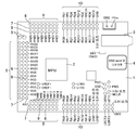
- FIG. 46 shows a conventional example of a base board provided with a microcomputer as a signal processing unit.
- a microprocessor 2 constituting a microcomputer is mounted, and other necessary circuit elements are mounted.
- the base board 1 has a power supply terminal + Vcc and a ground terminal GND for receiving supply of DC power from an external power supply, a microphone jack 3 for inputting an audio signal, a speaker output terminal 5 which is an audio signal output terminal, USB It has a connector 4 and has an LED for displaying the operating state of the microcomputer.
- the base board 1 has an input / output terminal group 9 mainly used as an analog signal input terminal, and an input / output terminal group 10 of a communication system signal used for communication with the outside.
- the input / output terminal group 9 of the analog signal is disposed along the left edge and a part of the upper and lower edges in FIG. 46 of the base board 1.
- the ground terminal 6 is arranged closest to the edge of the base board 1 and then arranged in the order of the power supply terminal 7 and the signal terminal 8. All the ground terminals 6 are electrically connected integrally with the ground terminal GND, and all the power supply terminals 7 are also connected electrically integrally with the power supply terminal + Vcc.
- the signals input from the above signal terminals are input to the microprocessor 2, and the microprocessor 2 is configured to perform signal processing in accordance with software incorporated in advance.
- the input / output terminal group 10 of the communication system is formed as a pair of two terminals.
- FIG. 47 shows an example of connection between a base board provided with a conventional microcomputer and an expansion module.
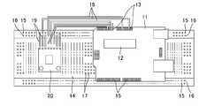
- the baseboard indicated by reference numeral 11 in FIG. 47 has a specification different from that of the baseboard 1 shown in FIG.
- the microprocessor 12 is mounted on the base board 11, and an appropriate number of connectors 13 are arranged on the side edge of the base board 11.
- the connector 13 may be connected to a ground or a power supply, or may be connected to the microprocessor 12 to input / output a signal to / from the microprocessor 12.
- the baseboard 11 is mounted on a breadboard 14.
- the breadboard 14 is a soldering-free substrate which can constitute an electronic circuit simply by inserting various electronic components and jumper wires and the like, and is generally used for experiment, evaluation or trial manufacture of the circuit. used.
- a number of ground terminal holes 15 connected to the ground line along these side edges are formed at regular intervals on a straight line.
- a number of power supply terminal holes 16 are formed in parallel with the 15 rows and paired with the terminal holes 15 and connected to the power supply line.
- the breadboard 14 has a row of holes consisting of a row of ground terminal holes 15 and a row of power terminal holes 16 on both sides in the longitudinal direction, and in the region sandwiched by the row of holes on both sides, a constant distance Innumerable terminal holes 17 are formed.
- a plurality of terminal holes 17 arranged in a row in the width direction of the breadboard 14, ie, the above-mentioned ground terminal hole row and the power terminal hole row form one set, and one set of terminal holes 17 They are integrally connected, and a large number of sets of terminal holes are arranged in parallel.
- the breadboard 14 is mounted with an expansion module 20 in which a circuit performing a specific function is built on a circuit board.
- the plurality of terminal pins provided in the expansion module 20 are respectively inserted into one terminal hole 17 of different terminal hole rows among a plurality of terminal hole rows arranged in the longitudinal direction of the breadboard 14. Accordingly, each one of the terminal pins of the expansion module 20 is electrically connected to the plurality of terminal holes 17 forming one set of the breadboard 14.
- One end of the jumper wire 19 is inserted into one of the pair of terminal holes 17 which are made conductive by inserting the ground pin of the expansion module 20, and the other end of the jumper wire 19 is one of the ground terminal holes 15.
- the ground pin of the expansion module 20 is connected to the ground line by being inserted into one.
- one end of the jumper wire 19 is inserted into one of the pair of terminal holes 17 which are made conductive by inserting the power supply pin of the expansion module 20, and the other end of the jumper wire 19 is a power supply By being inserted into one of the terminal holes 16, the power supply pin of the expansion module 20 is connected to the power supply line.
- one end of the wire 18 is inserted into one of a pair of terminal holes 17 which are conducted to the signal terminal by the insertion of the signal terminal, and the wire The other end 18 is inserted into a predetermined connector of the plurality of connectors 13 of the base board 11.
- the signal terminal of the expansion module 20 and the predetermined terminal of the microprocessor 12 or the predetermined connection point of the base board 11 are electrically connected.
- a plurality of wires 18 are provided, and a plurality of connection points of the base board 11 and a plurality of connection points of the expansion module 20 are connected through the connector 13 of the base board 11 and the wires 18 of the base board 11 and the terminal holes 17 of the breadboard 14.
- the conventional connection structure of the base board and the expansion module is a structure for drawing a wire. Also in the conventional base board shown in FIG. 46, one end of the wire is soldered to each terminal, or the wire is pulled out from the connector fixed on each terminal, and the other end of each wire is made into an expansion module It is soldered or connected via a connector.
- Patent Document 1 a plurality of first sets of connection boards provided parallel to each other and a plurality of component boards arranged in a direction orthogonal to the connection boards are provided at the edge of the component boards.
- a component board system is described which is adapted to be electrically connected by coupling the contact elements of and the second set of contact elements provided at the edge of the connection board.
- Patent Document 1 describes only a mechanical structure in which a connection board and a component board are directly connected by the engagement of first and second contacts corresponding to a pin and a jack of a connector. Connection relations are not described.
- a support to which a communication device is attached is configured by combining a plurality of pillars having a U-shaped cross section, and the power supply bus is housed inside the support, thereby expanding the wiring area on the back of the support.
- the power supply structure of the communication device capable of increasing the number of possible feeding cables and improving the workability of wiring is described.
- Patent Document 3 discloses a data communication system in which a plurality of devices are connected using an SPI device, which has a communication manager that arbitrates serial communication between a master device and a slave device, and is a serial arbitrated by the communication manager.
- a data communication apparatus is described in which communication is performed based on an appropriate physical protocol to each slave device via a communication interface. According to the invention described in Patent Document 3, by switching the communication protocol in accordance with the chip select signal line, it is possible to perform communication using the communication protocol optimum for each device.
- Patent Document 3 does not describe the coupling structure between a base board provided with a microcomputer and an expansion module.
- the present invention solves the problems of the conventional baseboard-expansion module coupling structure described above, ie, eliminates the wires connecting between the baseboard and the expansion module, simplifying the structure and connection operation. Even when trying to change the specifications, the baseboard, expansion module and baseboard and expansion module that can eliminate troublesome work such as removing the wire and re-installing the wire and can reduce wiring errors dramatically
- the purpose is to provide a bonding structure.
- a baseboard is a baseboard including a signal processing unit and an extension module performing a specific function is coupled, the baseboard including a first connector to which the extension module is coupled,
- One connector includes at least a ground terminal connected to the ground line, a power supply terminal connected to the power supply line, and a signal terminal connected to the signal line, and at least one ground terminal, one power supply terminal and one signal terminal are paired.
- a plurality of terminal sets are arranged at regular intervals on the base board as a terminal set to constitute a plurality of first connectors, and a connector of an expansion module is configured to be connectable to the first connector. It is a feature.
- An expansion module is an expansion module coupled to a base board including a signal processing unit to perform a specific function, and coupled to the first connector of the base board to couple to the base board.
- the second connector includes one ground terminal connectable to the ground terminal of the first connector, one power supply terminal connectable to the power supply terminal of the first connector, and the first connector.
- One signal terminal connectable to the signal terminal of the connector is constituted by a plurality of terminal sets as a set of terminal groups, and the second connector is configured such that the plurality of terminal sets constituting the second connector are the first connector. It is arranged at the same interval as the arrangement interval of the plurality of terminal sets to be configured, and is configured to be able to be coupled across the plurality of first connectors adjacent to each other. It is referred to as main features.
- the expansion module selects the second connector of the expansion module from among the first connectors of the base board and selects the first connector compatible with the expansion module, thereby coupling the baseboard to the baseboard.
- Mechanical coupling with the base board is performed, and the base board and the expansion module are electrically coupled.
- the ground terminal of the expansion module is connected to the ground line and the power supply terminal is connected to the power supply line via the first and second connectors.
- the expansion module can be electrically coupled to the base board without drawing a wire, and the coupling structure between the base board and the expansion module can be simplified and the coupling workability can be improved.
- the example of the various connection aspect of a base board and an expansion module is shown, (a) is a perspective view, (b) is a side view which shows another aspect. It is a side view showing still another various connection modes of a baseboard and an expansion module. It is a side view which shows another connection aspect of a base board and an expansion module. It is a circuit diagram showing an example of a substrate for I2C compass module applicable to the present invention. It is a top view of the adapter board for said I2C compass modules. It is a circuit diagram showing an example of an adapter board for I2C inertial posture measurement (IMU) module applicable to the present invention.
- IMU inertial posture measurement
- FIG. 6 is a circuit diagram showing an example of a pull-up resistive cap required when using an I2C module as an expansion module. It is a top view of the above-mentioned pull up resistance cap. It is a block diagram which shows the general structure of SPI communication.
- FIG. 16 is a plan view showing an example of the SPI communication module substrate in the case of using a demultiplexer for designating the SPI communication module when using a plurality of SPI communication modules in an overlapping manner as an extension module.
- the example of the said demultiplexer is shown, (a) is a circuit diagram, (b) is a truth table.
- FIG. 13 is a plan view schematically showing an example of the SPI communication module in the case of using a single pin signal for designating the SPI communication module when a plurality of SPI communication module substrates are stacked and used as an extension module.
- FIG. 13 is a plan view schematically showing an example of the SPI communication module substrate in the case where I2C communication is used in combination for specifying the SPI communication module when a plurality of SPI communication module substrates are stacked and used as an extension module.
- FIG. 16 is a circuit diagram conceptually showing an example of the SPI communication module in the case of using a communication bus for designating the SPI communication module when using a plurality of SPI communication module substrates as an extension module in a stack. It is a circuit diagram showing an example of a signal processing circuit when piling up a plurality of expansion modules. It is a schematic diagram which shows notionally the result connected and connected to several devices among several expansion modules in the said example of a signal processing circuit.
- FIG. 6 is a circuit diagram showing a specific example of a circuit using an I2C I / O expander as a designated determination element. It is a block diagram which shows the example of a structure of the base board which can confirm the connection position of an expansion module. It is a block diagram which shows the flow of the signal in the example which connected the expansion module to the base board shown in FIG.
- FIG. 27 is a circuit diagram showing an example of a circuit of an extension module shown in FIG. 26. It is a top view which shows the example of another connection of a base board and an expansion module.
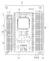
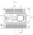
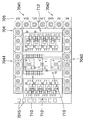
- FIG. 1 shows an embodiment of a baseboard according to the present invention.
- a microcomputer 102 is attached to one side of a base board 100 via a microcomputer board 101.
- a large number of connection pins 106 extend downward from both longitudinal side edges of the microcomputer board 101, and each connection pin 106 is a connector 105 fixed to the upper surface of the base board 100.
- the microcomputer board 101 is mounted on the base board 100 by being inserted into the board.
- connectors 110, 120, 140 are mounted on the upper surface of the base board 100 parallel to both longitudinal edges of the base board 100 and the connector 105 and outside the connector 105.
- the connectors 110 and 120 are disposed at one side edge of the base board 100, and the connector 140 is disposed at the other side edge of the base board 100.
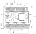
- the connectors 110, 120, and 140 each have at least a ground terminal connected to the ground line, a power supply terminal connected to the power supply line, and a signal terminal connected to the signal line. Further, there are a plurality of ground terminals, power terminals and signal terminals constituting the connectors 110, 120 and 140, and a plurality of sets of connectors are formed.
- the connectors 110, 120, and 140 will be described more specifically.
- the connector 110 includes eight sets of terminals each including a ground terminal, a power supply terminal connected to a power supply having a voltage of 4.8 to 6.0 V, and a signal terminal.
- the eight ground terminals constituting the eight terminal sets constitute the ground terminal set 111, and similarly, the eight power terminals constitute the power terminal set 112, and the eight signal terminals are the signal terminal set 113. are configured.
- the connector 120 includes eight sets of terminals each of which is a ground terminal, a power supply terminal having a voltage of 3.3 V or 5 V, and a signal terminal.
- the eight ground terminals constituting the eight terminal sets constitute the ground terminal set 121
- the eight power terminals constitute the power terminal set 122
- the eight signal terminals constitute the signal terminal set 123. ing.
- the connector 140 includes 16 sets of terminals each including a power supply terminal having a voltage of 5 V, a ground terminal, a power supply terminal having a voltage of 3.3 V, and a signal terminal.
- Sixteen 5 V power terminals constituting the 16 terminal sets constitute a power terminal set 141
- 16 ground terminals constitute a ground terminal set 142
- 16 3.3 V power terminals are a power supply.
- the terminal set 143 is configured, and the 16 signal terminals form a signal terminal set 144.
- the terminal sets constituting the connectors 110, 120 and 140 are aligned at regular intervals, and the ground terminals, power terminals and signal terminals constituting all the terminal groups are aligned at regular intervals on a straight line, and all terminals Are arranged in a matrix.
- the connectors 110, 120, and 140 attached to the base board 100 are coupled to connectors on the expansion module side described later. Therefore, the connectors 110, 120, and 140 are used as the first connector, and the connector on the expansion module side coupled thereto is used as the second connector.
- the first connectors 110, 120, and 140 are all female or jack-type. However, depending on the correspondence with the second connector on the expansion module side, it may be of a male type, that is, a plug type or a pin type.
- each signal terminal of the first connectors 110, 120, and 140 has a circuit pattern of the base board 100, a circuit pattern of the connector 105, the connection pin 106, and the circuit pattern of the microcomputer board 101 described in FIG. It is electrically connected to the corresponding terminal of the computer 102.
- the base board 100 is provided with 3.3 V and 5 V power input terminals.
- the microcomputer board 101 is provided with a display comprising an LED or the like indicating the operation state of the microcomputer, a USB jack, and other circuits, but the depiction is omitted in FIG.
- FIG. 3 shows an example of types and types of expansion modules connectable to the first connectors 110, 120, 140.
- a first connector indicated by reference numeral 110 is a connector for a radio control (hereinafter sometimes referred to as "RC") servo connector, and each power supply terminal is connected to a 5V power supply line.
- the first connector indicated by reference numeral 120 is divided into a connector group A for cable connection modules and a group connector B for cable connection modules every four terminal groups. Each power supply terminal belonging to group B is connected to a power supply line of voltage 3.3V, and each power supply terminal belonging to group A is connected to a power supply line of voltage 5V.
- a first connector indicated by reference numeral 140 is for connection of a sensor module or the like, and has a total of 16 terminal sets, each terminal set being a power supply terminal connected to a 3.3V power supply line and a 5V power supply line Power supply terminal connected to the
- FIG. 4 conceptually illustrates that the expansion module substrate is coupled to the base board 100 having the first connectors 110, 120, and 140.
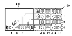
- reference numeral 200 indicates an adapter substrate for I2C compass module for connecting the I2C compass module on which the orientation sensor is mounted to the base board 100.
- the adapter substrate 200 has a second connector 201 coupled to four sets of terminals of the first connector 140, as shown in FIG. By fitting the second connector 201 into the first connector 140, the base board 100 and the adapter substrate 200 for I2C compass module are physically coupled and electrically connected.
- Reference numeral 210 in FIG. 4 denotes a LAN connector module.
- the substrate of the LAN connector module 210 has a second connector 211 which is coupled to the eight sets of terminals constituting the first connector 120. By fitting the second connector 211 into the first connector 120, the base board 100 and the LAN connector module 210 are physically coupled and electrically connected.
- FIG. 5 shows an example of an aspect in which substrates of a plurality of expansion modules are stacked.
- a first connector 140 in which the plurality of terminal sets described above are arranged is fixed on the surface (upper surface in FIG. 5) of the base board 100.
- the first connector 140 is a female type (jack)
- a connector formed of a male type (pin type) terminal 145 corresponding to each terminal of the female type protrudes on the back surface side of the base board 100.
- the expansion module can be physically and electrically coupled to the base board 100 by fitting a female connector (jack) of the expansion module to the terminal 145.
- the pin connector of the expansion module as the second connector can be fitted to the first connector 140 of the base board 100.
- reference numerals 151 and 155 indicate expansion modules incorporated in the circuit board, and reference numerals 153 and 157 indicate pin type terminals as second connectors projecting on the back side of the expansion modules 151 and 155, respectively. It shows.
- Each expansion module 151, 155 has a female connector (jack) 152, 156 composed of a terminal corresponding to each of the pin type terminals on the surface side.
- the configuration of the female connectors 152, 156 is the same as the configuration of the first connector 140 of the base board 100, and the second connector of another expansion module can be fitted to these connectors 152, 156.
- the female connector included in the module is also referred to as a first connector.
- a pin type terminal 162 which is a second connector of another expansion module 160 is fitted to a first connector 152 provided in the expansion module 151.
- the expansion module 160 also includes the first connector 161, and by inserting the second connector of another expansion module to the first connector 161, the expansion modules can be stacked in layers. ing.
- the baseboard 100 and the plurality of expansion modules physically coupled and stacked by fitting the first connector and the second connector are also electrically coupled via the first and second connectors.
- a part of the pin type connector may be exposed. The exposed connector pins can be brought into contact with the probe of the measuring machine or testing machine for measurement, testing, or inspection.
- the plurality of male terminals 145 protruding on the back surface side of the base board 100 constitute a connector.
- a female connector 146 can be coupled to this connector as needed, and another expansion module 147 can be connected to the base board 100 via the female connector 146.
- the connector formed of the male terminal 145 is a first connector
- the female connector 146 on the expansion module 147 side is a second connector.
- the male terminal 145 on the back surface side of the base board 100 may be cut if unnecessary.
- the plurality of expansion modules may be stacked in a zigzag manner by arranging the positions of the second connector and the first connector of the expansion modules at opposite edges.
- FIG. 7 (b) shows an example thereof.
- the second connector 174 provided on the back surface of one side edge of the expansion module 170 is fitted to the first connector 140 of the base board 100, and the first connector 175 is provided on the surface of the edge opposite to the second connector 174.
- the second connector 182 of another expansion module 180 is fitted to the first connector 175, thereby stacking the base board 100 and the two expansion modules 170, 180 in a zigzag manner.
- the expansion modules 170 and 180 respectively have first connectors 173 and 181 on opposite sides of the second connectors 174 and 182 with the base of the expansion modules 170 and 180 interposed therebetween.
- the second connector of another expansion module may be fitted to the first connector 173, 181.
- the first connector 410 included in the circuit board 400 is a male connector consisting of a plurality of pins rising from the circuit board 400, and the plurality of pins are bent by 90 ° and directed in the horizontal direction. ing.
- the tip surfaces of the plurality of horizontally oriented pins are on the same vertical plane and are equally spaced in the vertical direction.
- the second connector 404 of the expansion module 401 is fitted to the first connector 410.
- the expansion module 401 includes a second connector 405 composed of a plurality of pins at a position corresponding to the second connector 404 with the substrate of the expansion module 401 interposed therebetween.
- the expansion module 402 includes the second connector 406 and the first connector 407
- the expansion module 403 includes the second connector 408 and the first connector 409.
- the expansion module 402 fits the second connector 406 into the first connector 405 of the expansion module 401
- the expansion module 403 fits the second connector 408 into the first connector 407 of the expansion module 402.
- the three expansion modules 401, 402, 403 are stacked and coupled in parallel on the circuit board 400 in the vertical orientation.
- the circuit board 400 may be a base board.
- the expansion module has the first connector and the second connector on the opposite edge and on the opposite surface to connect a plurality of expansion modules in series.
- the base board 100 has the first connector 110 at one side edge, and the second connector 145 is provided on the opposite side of the first connector 110 with the base board 100 in the same manner as the above-mentioned example.
- the second connector 174 of the expansion module 170 is fitted to the first connector 110, and the first connector 175 provided at the edge of the expansion module 170 opposite to the second connector 174 is a separate one of the expansion modules 180.
- the second connector 182 is fitted.
- the base board 100 and the two expansion modules 170 and 180 are stacked in a folded manner.
- the second connector 412 of the expansion module 410 is fitted to the second connector 145 of the base board 100, and the second expansion module 170 and the above-mentioned two expansion modules 170 and 180 are stacked so as to be folded.
- the expansion module 410 has a first connector 411 at the edge opposite to the attachment edge of the second connector 412 and on the opposite side, and the first connector 411 is the second of the other expansion modules. The connector can be fitted.
- the expansion module has the first connector and the second connector on opposite edges and on the same surface, and a plurality of expansion modules are spread laterally while spreading horizontally. It is an example connected in series.
- male first connectors 421, 431, 441, and 451 are provided on one side edge of the same surface, and the other side is provided on the other side. It has a female second connector 422, 432, 442, 452.
- the first connector 421 of the expansion module 420 and the second connector 432 of the expansion module 430 are fitted, the first connector 431 of the expansion module 420 and the second connector 442 of the expansion module 440, and the first connector 441 of the expansion module 440.
- the second connector 452 of the expansion module 450 are fitted. Therefore, the four expansion modules 420, 430, 440, and 450 are coupled in series while being alternately inverted.
- the second connector 422 of the rightmost expansion module 420 can be fitted to the male first connector of the baseboard.
- the first connector 451 of the leftmost expansion module 450 in FIG. 8C can be fitted to the female first connector of the baseboard.
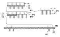
- the width of the expansion module located in the middle of the stacking direction may be smaller than the width of the expansion modules to be stacked thereon.
- an example shown in FIG. 9 is devised so that the layers can be stacked without any problems.
- the second connector 153 of the expansion module 151 is fitted to the first connector 140 provided at one side edge of the base board 100, and the first connector 152 of the expansion module 151 inserts another extension module 460.
- the second connector 463 is adapted to be fitted.
- the width of the expansion module 151 is smaller than the width of the expansion module 460, and the expansion module 460 is superimposed on the expansion module 151, some of the plurality of pin terminals constituting the second connector 463 of the expansion module 460 It protrudes from the first connector 152 of the expansion module 151, does not fit in either the connector or the connector of the base board 100, and floats in the air.
- an auxiliary connector 470 for inserting a pin-type terminal of the expansion module 460 protruding from the first connector 152 of the expansion module 151 is added.
- the auxiliary connector 470 has a second connector 472 consisting of a pin type terminal and a female first connector 471 and does not have a circuit board, and the exposed portion of each terminal is increased as there is no circuit board. There is.
- the auxiliary connector 470 has a sufficient size or number of terminals to complement the plurality of pin-type terminals protruding from the first connector 152 of the expansion module 151.
- the auxiliary connector 470 is fitted to the first connector 140 of the base board 100 in contact with the expansion module 151, and the expansion module 460 is fitted over the expansion module 151 and the auxiliary connector 470. In this manner, all terminals of the expansion module 151 and the expansion module 460 can be coupled to the base board 100.
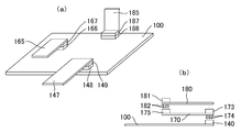
- connection position of the expansion module with respect to the base board 100 and the posture of the connected expansion module are arbitrary.
- FIG. 7 (a) shows these various aspects.
- the expansion module 147 has its second connector 149 fitted to the first connector 148 disposed along one side edge of the baseboard 100 so that the side from the one side edge of the baseboard 100 can be extended. It is coupled to the motherboard 100 in a manner that projects towards the side.
- the expansion module 165 is coupled to the baseboard 100 in such a manner as to be positioned within the projection plane of the baseboard 100 by fitting the second connector 167 to the first connector 166 disposed inward of the baseboard 100.
- the expansion module 185 is coupled to the baseboard 100 in a posture rising from the surface of the baseboard 100 by setting the fitting direction of the second connector 187 to the first connector 186 as the surface direction of the expansion module 185.
- connection mode of the expansion module to the base board 100 and the stacking mode of the plurality of expansion modules are variously conceivable and can be arbitrarily changed.
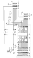
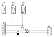
- FIG. 10 shows the electrical connection between the terminals of the second connector 201 of the adapter substrate 200 for I2C compass module for connecting the I2C compass module to the base board 100.
- the adapter substrate 200 for I2C compass module is provided with four terminals indicated by reference numeral JP1 in FIG. 11, and the I2C compass module is mounted on these four terminals by an appropriate means such as soldering.
- the second connector 201 is a power supply terminal row JP6 fitted to the 5V power supply terminal row 141 (see FIG. 1) of the baseboard 100, and a ground terminal row JP5, 3.3V power supply fitted to the ground terminal row 142 (see FIG. 1).
- a power terminal row JP4 fitted to the terminal row 143 see FIG.
- the adapter substrate 200 for I2C compass module uses a 3.3 V power supply, and therefore, is not wired to the 5 V power terminal row JP6 as shown in FIG.
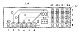
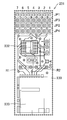
- FIG. 13 shows the adapter substrate 220 for I2CIMU module coupled to the first connector 140 of the base board 100
- FIG. 12 shows the electrical connection between the respective terminals of the second connector 221.
- the IMU module is connected to the I2CIMU module adapter substrate 220.
- the IMU module is a module provided with at least one of a 3-axis acceleration sensor, an angular velocity sensor (gyro), and a geomagnetic (orientation) sensor.
- the second connector 221 included in the adapter board 220 for I2CIMU module is fitted to the power terminal row JP1 and the ground terminal row 142 (see FIG. 1) fitted to the 5 V power terminal row 141 (see FIG.
- the ground terminal row JP3 has a power terminal row JP2 fitted to the 3.3 V power supply terminal row 143 (see FIG. 1) and a signal terminal row JP4 fitted to the signal terminal row 144 (see FIG. 1).
- the I2CIMU module adapter substrate 220 includes six terminals indicated by reference numeral JP5 in FIGS. 12 and 13, and the I2CIMU module is mounted on the six terminals by an appropriate means such as soldering.
- the I2CIMU module adapter board 220 is configured to use a 3.3V power supply and is not wired to the 5V power supply terminal row JP1.
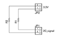
- the pull-up resistance substrate 250 shown in FIGS. 18 and 19 is stacked on the adapter substrate 220 for I2C module coupled to the base board 100 by fitting the first and second connectors.
- the pull-up resistor board 250 includes a second connector 251 that fits into the first connector provided in the adapter board 220 for I2C module.
- the second connector 251 has a terminal row JP2 consisting of two terminals respectively connected to two signal lines, and two terminal rows JP1 connected to two power supply lines, and between each one signal terminal and the power supply terminal Are connected to the pull-up resistors R1 and R2.
- the signal line of the I2C module is pulled up, and the I2C module performs a predetermined function.
- the pull-up resistor substrate 250 can also have various connection modes as the substrate of the expansion module. Besides pull-up, the present invention is also applicable to signal lines that need to be pulled down.
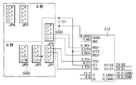
- FIG. 15 shows an example of the substrate of the LAN connector module 210
- FIG. 14 shows the electrical connection between the terminal array of the second connector 211 provided on the substrate of the LAN connector module 210 and the control element 212.
- the terminals of the second connector 211 of the LAN connector module 210 are coupled to the terminals of the first connector 120 of the baseboard 100 shown in FIG.
- the first connector 120 is divided into a cable connection module connector group A and a cable connection module group B every four sets of terminals.
- the second connector 211 of the LAN connector module 210 has the signal terminal row JP1 coupled to the connector of the group B, the power supply terminal row JP2 of 3.3 V, and the ground terminal row JP3, and the connector of the group A A signal terminal row JP4 to be coupled, a 5V power supply terminal row JP5, and a ground terminal row JP6 are provided.
- the LAN connector module substrate 210 may be removed to reduce size and weight. .
- FIG. 17 shows an example of the SD card module 230 of SPI communication specification
- FIG. 16 shows the terminal row of the second connector 231 provided on the substrate of the SD card module 230, the chip select IC 232, and the SD card 233.
- SPI is a synchronous serial communication method in which communication is performed between a master and a slave by three signal lines of a clock SCK, unidirectional write data SO and read data SI, and among a plurality of slaves, SPI is known.
- Chip select (CS) or slave select (SS) signal lines are added to select a specific slave.
- a 3.3V power supply voltage is divided by the resistors R1 and R2 and input to the designated determination element 232 made of a chip select IC or the like. This voltage value is set to be the designated address number of the module.
- the SPI module 230 enters the sleep mode.
- the 2nd and 3rd pins of the jumper wire pin SJ2 shown in FIG. 16 are short-circuited, and the voltage inputted to the designated judging element 232 is made a voltage other than 0V.
- the chip select (CS) pin (4 terminals of JP1 shown in FIG. 16) is enabled and a voltage value inputted as a designated address setting value is designated by SPI communication.
- the SD card 233 can be effectively functioned by these operations. If you want to use the conventional chip select function, short 1 and 2 of jumper wire pin SJ2.
- the expansion module can stack a plurality of modules, which can be combined with the base board 100 to provide more complex functions.
- the extension module is an SPI communication specification, it is necessary to transmit a signal for selecting each extension module so that a predetermined extension module operates.
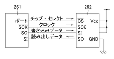
- FIG. 20 shows an outline of SPI communication.
- the master 261 and the slave 262 are connected by four signal lines of a chip select signal line, a clock signal line, a write data line, and a read data line.
- the chip select signal is a signal transmitted from the master 261 to the slave 262 for selecting a specific slave.
- the clock signal is a signal transmitted from the master 261 to the slave 262 in order to operate the master 261 and the slave 262 in synchronization.
- the write data is a data signal output from the master 261 to the slave 262.
- the read data is a data signal input from the slave 262 to the master 261.
- a method of stacking using an output terminal module for chip select (2) A method of identifying at the module side using one signal line by a single pin. (3) A method of selecting using I2C and SPI communication in combination. (4) A method of setting a specification of a module by a communication bus.
- the demultiplexer comprises an input terminal of one data D0, an input terminal of several selection control signals A and B, and a plurality of output terminals Y0, Y1, Y2 and Y3.
- the logic circuit sends out the input data D0 to one of the output terminals Y0, Y1, Y2, Y3 in accordance with the input values of the selection control signals A, B.
- FIG. 22 (b) shows a truth table of the demultiplexer.
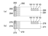
- FIG. 21A shows an output terminal module for chip select using a demultiplexer
- FIG. 21B is a conceptual view of an SPI module stacked on the output terminal module for chip select.
- the patterns of signal lines connected to the two terminals 285 shown in FIG. 21A are outputted to the respective terminals Y0 to Y3 of the connector 286 by using a demultiplexer circuit.
- the signal pin corresponding to D0 in FIG. 22 is input as a fixed signal from the power supply in the module.
- the modules (a) and (b) shown in FIG. 21 are stacked so that the connectors 284 and 274 and the connectors 286 and 276 which these modules have are electrically connected.
- the chip select output terminal module shown in FIG. 21B has a jumper or switch electrically connecting one of its terminals 275 with one of the terminals Y0 to Y3 of the connector 286 shown in FIG. And so on.
- the terminal 275 is selected as an input, it is used when directly connecting to the base board without using the chip select output terminal module, that is, without stacking other modules.
- any one of the terminals Y0 to Y3 of the connector 276 of the chip select output terminal module is electrically connected and connected to the chip select pin of the SPI element.
- the module 281 shown in FIG. 21 (a) is connected to the baseboard, and the module 271 shown in FIG.
- 21 (b) is stacked on the module 281 shown in FIG. 21 (a). Corresponding connectors are coupled together. Thus, in the example shown in FIG. 21, up to four stacked signals of two signals from the base board (the signals of the two terminals 285 of the module shown in FIG. 21A) via the chip select output terminal module. Any chip can be selected from the modules.
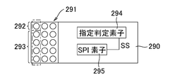
- FIG. 23 schematically illustrates an SPI module 290 that can be identified in the manner described above.
- the second terminal 291 included in the SPI module 290 has four signal terminals, and one of the terminals 292 is a signal terminal for designating the SPI module.
- the signal terminal 292 is connected to the designated determination element 294.
- the designation determination element 294 When it is determined by the designation determination element 294 that the SPI module 290 is designated, the designation determination element enables the signal pin SS (Slave Select) in the SPI module 290 in order to designate the SPI element 295.
- One of the plurality of stacked SPI modules 290 is specified by the pulse width of the signal input from the signal terminal 292, the voltage, a combination thereof, or the like. In addition, it is convenient to set so that all SS pins become invalid at a specific address.
- the other three signal terminals 293 of the second terminal 291 having four signal terminals are terminals for outputting or inputting the signals SCK, MISO and MOSI for SPI communication.
- a plurality of SPI modules 290 can be stacked and connected in a beaded connection, and one SPI module 290 can be selected by a signal input from the signal terminal 292. If an address for specifying a module is designated in advance in the SPI module 290, it can be connected in a daisy chain like an I2C module.
- the designation address of the module may be set in advance in a microcomputer or the like, but may be designated by a jumper wire, a switch, a ROM, a resistance value, a voltage value obtained by dividing the resistance, or the like.
- a designated determination element 294 which can designate the SS or CS pin of the module according to the signal of the single pin (the above-mentioned terminal 292) in order to receive a signal for designating one SPI module 290, It is good to mount a small microcomputer etc. which saved the program. It is good to make SPI module correspond to such a specification.
- a circuit may be provided to enable or disable the SS (CS) pin for the magnitude of the analog signal, for example, the signal level.
- the designated address of the SPI module may be designated by any method described above. Input / output of signals between the designated SPI module 290 and the base board is performed through three signal terminals 293 shown in FIG. The functions of the modules identified by the method according to (2) described above may be integrated into one chip.
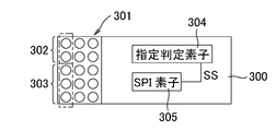
- FIG. 24 schematically illustrates an SPI module 300 that can be identified in the manner described above.
- the second connector 301 provided in the SPI module 300 has five signal terminals, of which two terminals 302 are I2C signal terminals for designating the SPI module.
- the remaining three terminals 303 are signal terminals for input and output of SPI signals.
- the SPI module 300 is also equipped with a device 304 that can utilize I2C.
- a plurality of modules can be connected in a cascade by the signal terminals 302 and 303.
- the SPI module 300 can be stacked in plural and connected in a beaded connection, and one SPI module 300 can be selected by a signal input from the signal terminal 302. If a designated address of the module (which device is designated) is designated in advance in the SPI module 300, a simple beaded like an I2C module without being aware of signal lines such as chip select (CS) Can be connected to Further, the designated address of the SPI module may be selected from any of the foregoing designation methods.
- the functions of the modules identified by the method according to (3) described above may be integrated into one chip.
- FIG. 25 shows an example of signal input / output between an SPI communication module implementing this method and this module.
- each module 310 includes a second connector 311, a designated determination element 315, and an SPI element 316.
- Each second connector 311 has four sets of terminal sets, and one of four signal terminals 312 is a designation signal input terminal for designating designation judgment element 315, and the remaining three terminals 313 are SPI. Signal input / output terminal.
- a designated judgment element designation signal is input to the designated judgment element designation signal input terminal 312 from the baseboard 100 side, and the designation judgment element 315 of each module 310 performs SPI communication to judge whether it matches the address set in the module. Then, it is determined whether or not each module 310 is specified, and the specification determination element 315 enables or disables the SS pin of the SPI element 316.
- Signals CLK, MOSI, and MISO corresponding to the respective terminals are input / output from the SPI signal line 320 to the three terminals 313 of each module 310, and according to these signals, the designated determination element 315 and the designated module
- the SPI element 316 included in 310 is adapted to operate.
- the designation signal input terminal 312 in FIG. 25 is connected only to the designation determination element 315, and is not connected to the SPI element 316. Further, both the designated determination element 315 and the SPI element 316 are connected to SPI buses (clock, data input, data output) of three terminals 313. The designated determination element 315 is connected to the slave select SS (or chip select CS) of the SPI element 316.
- the address data is sent from the base board to the designated determination elements 315 of all the stacked modules 310 by SPI communication, and the designated determination element 315 determines whether it matches the address set in advance. If they coincide with each other, the designated determination element 315 validates SS (CS) of the SPI element at the same time as the designated signal input terminal 312 becomes invalid. When the designation signal input terminal 312 becomes valid again, the designation determination element 315 invalidates SS (CS) of the SPI element 316. Thereafter, the designated determination elements of all the stacked modules are waiting for SPI data input from the baseboard, and the above process is repeated.
- the base board When the expansion modules are stacked, the base board is in SPI communication simultaneously with the plurality of specification determination elements 315 when the specification signal input terminal 312 of the expansion module 310 is enabled. At this time, if it is possible to make a response from the expansion module 310 to the base board, a terminal for outputting data from the designation determination element 315 by SPI so that terminals for outputting data by the SPI communication of the designation determination element 315 do not short. In addition, it is necessary to attach an appropriate resistor or a diode for preventing short circuit.
- the SPI signal line is three lines of CLK, MOSI, and MISO, and bi-directional communication is performed between the baseboard and the extension module 310, but from the baseboard If one-way communication to the expansion module 310 is to be performed, it is sufficient to have two lines excluding the data output signal from the expansion module.
- the signal processing procedure of the method (4) will be described.
- the designated judgment element designation signal connected to the designated judgment element designation signal input terminal 312 is made effective, all the chip select SS (CS) of the SPI element 316 are invalidated, and all the designated judgment elements 315 of all the stacked modules 310 are selected.
- Enable SPI communication In this state, a signal for designating a module is input to the designated determination element 315 by SPI communication. This designation signal is, for example, like an I2C address.
- the specification of the module completes the reservation for enabling the SPI element 316 of the specific module 310.
- the SS (CS) pins of the SPI devices 315 of all the stacked modules 310 are invalid.
- an echo is returned from the designated determination element 315 by SPI communication when the designated module 310 exists, processing in the case where there is an error is facilitated.
- the SPI element 316 connected to the three terminals 313 can communicate with the base board in SPI. Thereafter, the SPI element 316 of the designated SPI module 310 performs SPI communication with the base board 100 to read and write signals.
- the designated address of the SPI module may be previously set in a microcomputer or the like, but may be designated by a jumper wire, a switch, a ROM, a resistance value, a voltage value obtained by dividing a resistance, or the like.
- the designation determination element 315 invalidates SS (CS) of the SPI element 316, and the designation determination elements 315 of all the stacked modules 310 are subsequently repeated by repeating the above operation. It waits for SPI data input from the baseboard.
- the function of the module identified by the method according to (4) described above may be integrated into one chip.
- the expansion module is coupled to the base board simply by coupling the first connector on the base board side and the second connector on the expansion module side.
- the connection structure between the base board and the expansion module can be simplified and the connection workability can be improved.
- the ground and power terminals of the expansion module are connected to the ground and power lines via the first and second connectors, and these ground and power lines are connected to the ground and power lines of the base board, and the base board
- the signal line of the expansion module is connected through the signal terminals of both the first and second connectors.
- the row of ground terminals 111, 121 and 142 which form the first connectors 110, 120 and 140 of the base board 100 in the illustrated embodiment, the row of power terminals 112, 122 and 143, the signal terminals 113, 123 and 144, respectively.
- the arrangement of the line of lines and the line of other power terminals 141 constituting the first connector 140 is optional, and is not limited to the order of illustration as described above. Further, by changing the arrangement of the power supply terminal rows, for example, it is possible to connect an existing connector of a commercially available RC servo. It may have several first connectors with different arrangements of the ground terminal row, the power supply terminal row, and the signal terminal row.
- the second connector on the expansion module side has a specification corresponding to the specification of the first connector to which it is to be coupled.
- the first connector and the second connector may have at least a ground terminal connected to the ground line, a power supply terminal connected to the power supply line, and a signal terminal connected to the signal line.
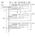
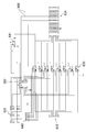
- FIG. 26 shows an example of a signal processing circuit, which has a plurality of SPI modules 510 as expansion modules, and each expansion module 510 includes an SPI I / O expander as a designation determination unit 501 and an SPI device 506, each designation
- the determination unit 501 includes an address setting unit 502.
- Each designation determination unit 501 has MISO, MOSI, and SCK signal terminals as SPI signal terminals, and these terminals are connected to corresponding MISO, MOSI, and SCK terminals of one microcomputer 500.
- the microcomputer 500 includes a chip select signal terminal CS and a signal input / output terminal I / O as normal input / output terminals.
- the terminal CS is connected to the terminal CS of each designation determination unit 501 and the switched terminal of each switching circuit 503.
- Each designation determination unit 501 has a plurality of output terminals, and one output terminal is connected to be input as a control signal of the switching circuit 503.
- the switching circuit 503 operates like a kind of gate, and the signal from the terminal CS of the microcomputer 500 inputted to the above-mentioned switched terminal of the switching circuit 503 is A, the control signal from the designation judging section 501 is B. Then, the switching circuit 503 electrically connects the CS terminal and the SS terminal according to the control signal B, and the signal A passes through the switching circuit 503.
- an inverter 505 is connected behind the switching circuit 503, and the signal C inverted by the inverter 505 is input to the SS terminal of the SPI device 506.
- each designation determination unit 501 is connected to the switched terminal of another switching circuit 504.
- a signal input from the output terminal of the designation determination unit 501 to the to-be-switched terminal is E.
- An output signal D of the signal input / output terminal I / O of the microcomputer 500 is input to the control terminal of the switching circuit 504.
- the switching circuit 504 electrically connects the CS terminal and the SS terminal by the signal E from the designation determination unit 501
- the signal D is input to the signal input / output terminal I / O of the SPI device 506.
- the SPI signal terminal of the microcomputer 500 is connected to the SPI signal terminal of each SPI device 506.
- the microcomputer 500 When the microcomputer 500 outputs the chip select signal CS, all the designation determination units 501 operate.
- the microcomputer 500 also transmits an SPI signal specifying one of the SPI modules 510.
- the specification determination unit 501 of each module determines whether the SPI signal is a signal specifying itself by comparing with an address signal set in the address setting unit 502 in advance, and specifies the device itself. In some cases, an instruction by the SPI signal is output from its output terminal.
- One of the output signals B opens the gate of the switching circuit 503 and passes the signal A, that is, the CS signal. Thereafter, there is no designation change of the input / output terminal I / O by communication, or the on state of the signal B is held unless the designated state is reset.
- the signal passed through the switching circuit 503 is inverted by the inverter 505 to be the inverted signal C, and the signal C is input to the SS terminal of the SPI device 506 in the SPI module 510.
- the SPI device 506 when the microcomputer 500 operates the designation determination unit 501, the SPI device 506 is invalidated.
- the designation determination unit 501 permits the connection from the microcomputer 500 and disables the signal CS of the designation determination unit 501, the SPI device 506 operates effectively.
- the effectively operating SPI device 506 performs a specific function based on the command signal from the microcomputer 500. Table 1 below shows the chip select logic of the SPI device.
- the SS terminal may be directly controlled by a signal from the designation determination unit 501.
- a plurality of devices operated by the chip select signal (CS) may exist in one expansion module.
- a switching circuit similar to the above switching circuit may be attached to a communication bus with a device (such as a microcomputer) of the expansion module to perform on / off control.
- the SPI device 506 may require input / output terminals in addition to the terminals connected to the SPI bus line and the chip select line. This can also be realized by a method almost similar to the aforementioned chip select method.
- Normal chip select signal terminals are not special terminals, and often use microcomputer input / output terminals. That is, any ordinary input / output terminal of the microcomputer can be realized using any terminal.
- the I / O line from the microcomputer 500 is divided by the output signal E of the I / O expander which is the designation determination unit 501 into a second switching circuit comprising a relay, a logic circuit, an analog switch, etc.
- the configuration is such that it can be connected to the input / output terminal I / O of the SPI device 506 through 504.
- the difference from the chip select by the switching circuit 503 described above is the presence or absence of the inverter 505.
- the signal E from the designation determination unit 501 has a simpler circuit configuration in which permission to electrically connect the signal D and the signal F is given.
- FIG. 27 conceptually shows the execution result.
- FIG. 27 it is assumed that there are a plurality of, for example, “1” to “5” input / output terminals of the microcomputer 500, and a plurality of, for example, three expansion modules 510.
- connection permission with the microcomputer 500 is given to the terminals “1” and “5” by the operation of the I / O expander as the designation determination unit.
- the second expansion module 510 gives the terminal "4"
- the third expansion module terminal 510 gives the terminals "2", "3" and "5" connection permission with the microcomputer 500. Therefore, the terminal "5" is an example in which the same signal can be input / output of a plurality of modules in parallel.
- dashed lines with arrows indicate communication performed between microcomputer 500 and each expansion module 510 to control the designation determination unit in each expansion module 510.
- Signals transferred between the baseboard and each expansion module are not necessarily limited to digital signals in one direction, and may be analog signals, and both analog signals and digital signals may be treated as bidirectional signals. it can.
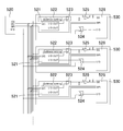
- each expansion module 530 includes a designation determination unit 521 including an I2C type I / O expander, an address setting unit 522, a first switching circuit 523, a second switching circuit 524, an inverter 525, and an SPI device 526. .
- This embodiment differs from the embodiment shown in FIG. 26 in that the microcomputer 520 and the designation judging unit 521 formed of an I2C type I / O expander are connected by an I2C bus, and the other configuration is the same.
- the specification determination operation of the expansion module 530 by the microcomputer 520 is also substantially the same as that of the embodiment shown in FIG.
- each designation determination unit can be controlled.
- the address setting of the designation determination unit may be any means such as an external circuit or a memory in an IC, as long as a specific value or the like can be set.
- connection examples of signal lines shown in FIGS. 26 and 28 and combining them with a plurality of expansion modules having a voltage holding circuit such as a peak hold circuit or a current holding circuit permission of the selected expansion module is obtained.
- the receiving terminal is switched to the terminal of another expansion module, the voltage or current of the analog terminal can be held at the terminal on the non-selected expansion module.
- the DA output and AD input can be continuously input / output from a plurality of modules by one DA (digital to analog conversion) terminal or AD (analog to digital conversion) terminal of the microcomputer.
- the voltage holding circuit or the current holding circuit may be reset using an input / output terminal such as an I / O expander or using an input / output terminal of a microcomputer.
- any periodic signal whether digital or analog, can be combined with the circuit that holds it.
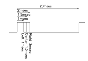
- FIG. 29 shows an example in the case of using one servo device
- FIG. 30 shows an example in the case of using a plurality of servo devices, for example, three servo devices. Any of them may be an expansion module configured as a servo device, and a dedicated circuit or a dedicated element is not necessary.
- PWM pulse width modulation
- operation for one channel is performed in 2 ms in one cycle of 20 ms, and the first 1 ms is a constant determined for identification.
- the angle of the RC servo is controlled within 1 ms of the pulse width in the latter half. For example, if the pulse falls within 1 ms-1.5 ms from the start of one cycle of 20 ms, 1.5 ms has elapsed from the start of the one cycle, if it falls to the left. If the pulse falls at this point, it is neutral or immobile, and if the pulse falls within 1.5 ms to 2 ms from the start of the one cycle, the rotation to the right is controlled.
- FIG. 30 shows an example in which three servo devices are used as the expansion module, and as described above, the control operation shown in FIG. 29 is performed while sequentially switching the servo devices in one cycle of 20 milliseconds. It is supposed to be repeated continuously.
- the control operation of each servo device is performed within 2 milliseconds as in the example shown in FIG. 29, and when 2 milliseconds elapse, the control operation of the next servo device is performed within 2 milliseconds and then the next The control operation of the servo device of the present invention is performed within 2 milliseconds.
- the control operation is similarly performed in the next period, and the same operation is repeatedly performed.
- FIG. 30 shows an example in which three servo devices are used as the expansion module, and as described above, the control operation shown in FIG. 29 is performed while sequentially switching the servo devices in one cycle of 20 milliseconds. It is supposed to be repeated continuously.
- the control operation of each servo device is performed within 2 milliseconds as in the example shown
- reference numeral 540 indicates the switching timing from module 1 to module 2, module 2 to module 3, and module 3 to module 1.
- Reference numeral 542 indicates a standby state until one cycle of the module 3 is finished and one cycle of 20 milliseconds elapses to switch to the module 1.
- a plurality of RC servos can be controlled by one terminal of one microcomputer.
- a circuit or element such as an I / O expander capable of PWM output may be directly connected to this circuit or element.
- signals may be output from terminals on the microcomputer side and fixed, and signals from the microcomputer may be controlled in a timely manner via switching circuits with signals from the module side I / O expander.
- the forward / reverse operation of the servo device is controlled at the fall timing of the pulse signal, but the operation of the servo device is controlled at the fall timing of the pulse signal. May be
- the function of the terminal of the microcomputer or the function of the terminal of the base board may be changed depending on the connected device.
- one or more terminals that were output in one expansion module may be input in another expansion module, or may be a communication bus when switching to the expansion module. This can also simplify hardware design to some extent.
- the substrate is assembled using the bonding structure according to the present invention. Later, if it is necessary to change the circuit design, it is only necessary to replace some of the expansion modules and rewrite the program, and it is not necessary to replace all the boards and parts, thus reducing the final operation cost. be able to. In addition, it is easy to respond easily when customizing some circuit functions, upgrading devices on individual expansion modules, or when you want to change some functions of input / output, etc. is there.
- the microcomputer By changing the specifications (specifications) of the microcomputer on the baseboard side, it is possible to operate at the optimum processing speed and the optimum cost according to the circuit configuration. This makes it possible to easily combine low-cost, wide variety of system products and even customized products. In order to achieve low cost, it is preferable to standardize the shape of the connector, the arrangement of the terminals of the communication bus, and the like so that the expansion module can be used around.
- the connecting part of the expansion module by the connector may be disconnected due to vibration etc.
- a hole for mounting is formed in all the expansion modules to be stacked, and a screw or the like is passed through the hole
- the substrates may be firmly coupled to each other and further fixed to a housing or the like in which the substrates are mounted.
- the replacement of the expansion module can be performed by replacing the connector portion with a designated position and writing the designated program, and can be easily replaced by a non-technical technician. Therefore, if a module to be replaced and a program to be written are specified, the expansion module can be replaced even if it is requested to a customer or a local outsourcing company, and the labor cost for operation can be reduced.
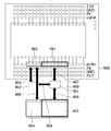
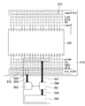
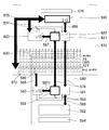
- FIG. 31 schematically shows an example of the connection between the extension module and the base board described above.
- the base board 560 shown in FIG. 31 includes power supply terminal rows of 3.3 V, ground terminal rows, power supply terminal rows of 5 V, and signal terminal rows from the outside toward the inside at the side edges in the length direction. Each of these terminal rows constitutes the above-described first connector.
- the expansion module 450 is physically and electrically coupled to one side edge of the base board 560 by the second connector of the expansion module 450 being fitted to the first connector.
- the second connector of the expansion module 450 is fitted to the first connector across the ground terminal row, the 5 V power terminal row, and the signal terminal row from the 3.3 V power terminal row of the base board 560.
- the extension module 450 includes the designation determination unit 453, the switching circuit 451, and the device 452 that performs a specific function, and further includes the device 454 including the same communication bus as the designation determination unit 453.
- the expansion module 450 includes a communication bus 456 connected to the communication bus 455 that operates on the same communication bus as the communication bus for designating judgment and the communication bus for designating judgment, and the input / output terminals of the baseboard 560 and switching circuits.
- a signal line 457 connecting 451, a signal line 458 connecting the switching circuit 451 and the device 452, and a signal line 459 connecting the designation determination unit 453 and the switching circuit 451 for permitting communication with the microcomputer are provided.
- Device 454 and device 452 may be the same as device 506 shown in FIG.
- the expansion module 450 has a second connector 561 consisting of seven terminals connected to seven specific signal terminals of the base board 560.
- the seven switching circuits 451 corresponding to the seven terminals, the devices 452 corresponding to the seven terminals selected by the switching circuits 451, and the designation determination unit 453 for controlling the seven switching circuits 451 Have.
- the expansion module 450 has a second connector 562 consisting of four terminals connected to four specific signal terminals of the base board 560 separately from the second connector 561.
- Each designation determination unit 453 determines the signal input from the signal terminal of the base board 560 via the second connector 562 and controls the corresponding switching circuit 451.
- a signal may be input to the device 454 through the switching circuit as needed. The device may be operated directly by the signal from the designation determination unit.
- switching circuits 451 and devices 452 are used in the example shown in FIG. 31, they are drawn in one block in order to avoid confusion of the drawings.
- the number of terminals of the base board 560 shown in FIG. 31, the size of the expansion module 450, and the like are arbitrary.
- a desired function can be provided only by stacking and connecting expansion modules 450 having the same configuration or expansion modules having different configurations.
- the signal terminals on the baseboard 560 side that can be used by the specification determination unit 453 of the expansion module 450 are only a part of the signal terminals arranged in a single line.
- the correspondence between the and the signal terminals of the expansion module 450 is limited. That is, the expansion module 450 needs to be connected to a specific position of the base board 560 in accordance with the communication line for controlling the designation determination unit, and if the connection position is incorrect, the correct operation can not be performed. .
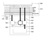
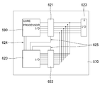
- a signal terminal row 572 that can be used for communication with the unit.
- the number of signal terminal rows 572 to be added may be one, two rows are provided in the example of FIG. 32 and two rows are respectively added to both side edge portions of the base board 570.
- the signal terminal rows 572 arranged in one row are electrically connected to each other, and four signal terminal rows 572 are provided.
- the four signal terminal rows are electrically disconnected from each other. Therefore, different signals can be input / output to the signal terminal row 572 of one row and the signal terminal row 572 of the other one row.
- the above-described configuration in which a plurality of modules are cascaded may be adopted.
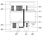
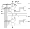
- the extension module 580 can introduce a designation signal to the designation determination unit 583 from the signal terminal row 572 via the second connector 589 and via the designation determination communication bus 585.
- the signal terminal row 572 capable of introducing a designation signal to the designation determination unit 583 is parallel to the power supply terminal row, like a bus line used in I2C, CAN, or other communication system in which several beads can be connected. Side by side.
- the designation judgment unit 583 and the extension module 580 are connected to any position in the longitudinal direction of the baseboard 560. Exchange of designated signals of
- the signal terminal row for specification determination is arranged with the power supply terminal row
- the power supply line and the specification element specification signal line can be made the same by using a technique such as power line communication such as PLC.
- the signal line for the designation signal is not necessary, and the configuration of the terminal row becomes compact.
- the board 600 is in the form of a base board not provided with a microcomputer, and substantially functions as an expansion module.
- the board 600 in the embodiment shown in FIG. 33 has a connector 611 consisting of a first connector and a second connector for stacking.
- a plurality of boards 600 are stacked and coupled by the connector 611, and the microcomputer 610 is mounted on the connector 611 of the upper board 600. It is also possible to stack a plurality of baseboard-like boards 600 by coupling the connector 611 with a connector of another board 600.
- Each of the boards 600 includes a designation determination unit 601, and includes switching circuits 602 and 603 and device groups 604 and 605 provided corresponding to the connectors 611 on both sides.
- the designation determination unit 601 determines and designates a terminal to be connected between the device and the microcomputer based on the signal of the signal line 606 connected to the specific terminal of the connector 611, and permits communication between the corresponding device and the microcomputer 610.
- the switching circuits 602 and 603 are controlled.
- the baseboard-like board 600 includes the device groups 604 and 605 having a specific function, and the example which has made it possible to stack the board 600 has been described above. It is different.
- the plurality of baseboard-like boards 600 can be stacked, and the microcomputer 610 can be connected to the devices 604 and 605 while switching the plurality of pins of the plurality of stacked boards 600.
- FIG. 34 shows an example in which the attachment position of the expansion module can be automatically determined.
- the base board 570 is configured in the same manner as the base board in the example shown in FIG. 32, and the signal terminal line 572 is provided in parallel with the power supply terminal line.
- the signal terminal row 572 may be a single row or a plurality of rows. Similar to the expansion module in the example shown in FIG.
- the expansion module 580 also includes a switching circuit 581, a device 582, a designation determination unit 583, and a connector 589 coupled to one terminal of each of the two signal terminal rows 572 described above.
- a switching circuit 581 is provided in FIG. 32.
- a second switching circuit 592 connecting the input / output terminal of the designation determination unit and the signal input / output terminal of the microcomputer 590 under the control of the designation determination unit 583 is provided. It is.
- the designation determination unit 583 controls the opening and closing of the switching circuits 581 and 592 in accordance with a designation determination signal input via the connector 589 and the designation determination communication bus 585.
- symbol 593 shows the control line of each said switching circuit 581,592.
- the second switching circuit 592 is a circuit for electrically connecting the input / output signal of the designation determination unit 583 itself to the baseboard 570 side, and the permission determination is also performed by the signal from the designation determination unit 583. Also in this example, a plurality of expansion modules 580 can be stacked and connected.
- the instruction judgment unit 583 receives an instruction from the microcomputer 590 side through the instruction judgment signal lines 572 589 585, invalidates the signal from the input / output terminal of the microcomputer 590 by the first switching circuit 581, and the second switching circuit 592 is valid.
- the second switching circuit 592 is valid, the input / output terminal of the microcomputer 590 and the input / output terminal of the designation determination element 583 are connected. In this state, the address of the designation determination unit 583 is designated, and a signal is output from the input / output terminal of the designation determination unit 583.
- this signal is received on the side of the base board 570 having the microcomputer 590, it can be determined to which address the expansion module 580 at which address is attached and at which position the input / output terminal. That is, the microcomputer 590 can automatically determine the circuit configuration, and can determine the exchange of signals for performing the desired function. Further, more precise operation can be realized by transmitting the signal of various information for using the number and type of terminals and the circuit of the expansion module from the designation determination unit according to the mounting position.
- FIG. 35 shows a specific example of a circuit using an I2C I / O expander as the designation determination unit 583.
- the configuration is the same as that of the example shown in FIG. 34, so the same components as those in the example shown in FIG. 34 are assigned the same reference numerals.
- the designation determination unit 583 may be any device other than the I2C I / O expander, as long as it performs a predetermined function by means of a communication system that can connect in small beads.
- the baseboard 570 side on which the microcomputer 590 is mounted shows which terminal the signal is output from. It can be detected.
- the position at which the expansion module 580 is connected can be grasped on the baseboard 570 side. Therefore, a certain expansion module 580 can be displayed with an LED or other indicator, such as the connection position is shifted.
- the microcomputer 590 controls the switching circuit to block the transmission of the data signal to the expansion module 580. Furthermore, if the correct connection position is displayed on the LED or other display unit, it can be easily recognized that the connection is incorrect, and it can be handled easily even by a non-expert.
- a control circuit 620 of the switching circuit and a third switching circuit 621 controlled by the control circuit 620 are provided on the base board 570 on which the microcomputer 590 is mounted.
- a fourth switching circuit 622 and a connector 623 for coupling the expansion module are provided as the control circuit 620.
- the control circuit 620 an I / O expander or the like can be used.
- the switching control circuit of the baseboard 570 is realized by disabling the third switching circuit 621 from the switching control circuit 620 disposed on the baseboard 570 and enabling the fourth switching circuit 622.
- the input / output terminal I / O 620 and the I / O of the designation determination unit of the expansion module can be electrically connected via the connector 623. In this state, if the input / output terminal of switching control circuit 620 is in the input state and the connector connection position confirmation signal from designation determination unit 583 on the expansion module is received, the microcomputer can not dynamically change the function of the terminal. , The connection position of the expansion module can be confirmed.
- FIG. 37 shows the flow of signals in an example in which the baseboard 570 shown in FIG. 36 and the expansion modules shown in FIGS. 34 and 35 are connected.
- a base board 570 includes a microcomputer 590, a switching control circuit 620, a third switching circuit 621, a fourth switching circuit 622, and a display portion 576 as in the example shown in FIG. .
- An expansion board 580 similar to the expansion board shown in FIG. 34 is coupled to the base board 570 by a coupling portion 630 formed of a first connector of the base board 570 and a second connector on the expansion board 580 side.
- the baseboard 570 includes a designation determination unit 583, a first switching circuit 581, a second switching circuit 592, a device 582 that performs a specific function, and a display unit 594.
- the microcomputer 590, the switching control circuit 620, the designation determination unit 583, and the switching circuits are all connected in a cascade by a signal bus.
- Reference numeral 574 denotes a control line of each switching circuit 621 622 in the base board 570
- reference numeral 593 denotes a control line of each switching circuit 581 592 in the expansion module 580.
- the signals to the signal buses 575, 572 and 585 for controlling the designation determination unit 583 and the switching control circuit 620 connected to the microcomputer 590 or the like are all the same signal. Also, the switching circuits 621, 622, 592, and 581 are controlled using the signal bus 578, the designation determination unit 583, and the switching control circuit 620.
- the switching circuits 592 and 622 are connected between the input / output of the designation determination unit 583 and the input / output of the switching control circuit 620 through the signal buses 587, 578 and 5871 or the microcomputer 590 and the expansion module 580
- the device group 582 is selected to be connected to the switching circuits 581 and 621 via the signal buses 588 and 578.
- Signal lines for controlling the switching circuit are represented by reference numerals 574 and 593.
- connection status display sections 576 and 594 display the connection status of the circuit, such as whether the connection position is correct.
- Control of the connection state display units 576 and 594 is performed from the baseboard 570 on which the microcomputer 590 is mounted to the input / output terminal I / O of the switching control circuit 620 or the input / output terminal I / O of the specification determination unit 583 of the expansion module 580. It may be performed based on the signal from O, or may be performed by the output signal of the input / output terminal of the designation determination unit 583 and the switching control circuit 620 according to the program provided in the microcomputer 590. In short, it does not matter if the connection position of the circuit or the connection state is known.
- an input / output terminal for receiving a position signal of expansion module 580 is separately provided on the side of base board 570, and this input / output terminal is connected to the input / output terminal of base board 570.
- a terminal connected to the input / output terminal of the designation determination unit may be provided.
- FIG. 38 shows a circuit example of the extension module 580.
- the expansion module 580 has the designation determination unit 583 as described above, the connector group 634 for coupling the expansion module 580 to the base board, and the switching circuit group 633 that plays the same role as the switching circuit 581; Display the input / output status of a switching circuit 641 similar to 592, an address setting unit 631, which presets a specific address to identify the module, an input / output terminal group 632 to a target device group, and a designation determination unit 583 And an input / output terminal 642.
- the connector group 634 is configured of a connector capable of stacking a plurality of expansion modules. To check the connection status of the expansion module, disable the switching circuit group 633, enable the switching circuit 641, output a voltage from a part of the expansion module terminals, and read the output on the baseboard side. It is good to display the result on the display unit.
- the command signal bus line 585 to the switching control circuit can be composed of one or more lines. Besides using this line for the designation determination unit 583, the connector provided for coupling the expansion module 660 to the baseboard 650 is provided with a power switch control signal terminal row 651 as shown in FIG. It can also be used to control relays and switch ICs that turn the 660 power on and off, and to control other device groups.
- the relays and switch ICs arranged in the expansion module 660 are on / off controlled by the switch circuit 661 for power on / off by the signal from the signal line connected to the power switch control signal terminal row 651, and the expansion module 660 It is also possible to switch the modules on the circuit after powering off the power supply. In this way, the expansion device 660 can be replaced without powering off the microcomputer.
- Each expansion module may be provided with a manual switch, and the manual switch may be configured to turn off the power and replace the expansion module without turning off the microcomputer.
- an instruction may be issued to the designation determination unit from the signal bus line for the designation determination unit, and the power switch of each expansion module may be operated.
- power on / off is controlled by a signal input / output via the power switch control signal terminal row 651, but in addition, a signal prompting to stop or reset the device may be used. . In short, it can be used to control the connected expansion modules 660 collectively.
- the microcomputer when turning off the power other than the microcomputer and changing the circuit configuration and then turning on the entire expansion module, the microcomputer is rebooted if it can be grasped which expansion module is coupled where by the method described above. It also becomes possible to easily switch over the expansion modules (or devices) present on the circuit without. It is also possible to test the operation while incorporating the circuit into the expansion module little by little. If a device or the like is desired to be operated constantly during replacement, the designation determination unit may forcibly send a signal to the power supply relay and power supply IC of the expansion module to keep it in the on state. The easiest way to turn off the power all at once is to turn the power supply line itself on or off automatically or manually using a relay, switch IC, or manual switch.
- the power switch circuit can be selected from the baseboard on which the microcomputer is mounted, the input / output terminal I / O of the switching circuit control circuit, the input / output terminal I / O of the designated determination unit of the expansion module, or the signal from the microcomputer itself It may be a circuit that is made to operate.
- the functions of the expansion module and the base board can also be applied to the base board 600 shown in FIG. Further, the configuration of the board 600 shown in FIG. 33 and various expansion modules may be combined and connected. For example, as shown in FIG. 40, a board 600 without a signal processing unit shown in FIG. 33 is connected to a lower stage than a base board 670 on which a board 675 including a microcomputer is mounted. Various expansion modules 680 may be coupled. The number of the boards 600 with respect to the base board 670 may be one or plural. In FIG. 40, reference numeral 672 denotes a connector for connecting the boards 600 to each other, and reference numeral 681 denotes a connector for connecting the expansion module 680 to the upper side of the base board 670.
- FIG. 41 shows an example of the circuit arrangement of the expansion module.
- the module configuration shown in FIG. 41 is configured based on an adapter substrate 700 for implementing the present invention.
- the adapter substrate 700 includes a second connector group 701 for coupling to the first connector on the base board side, a bidirectional analog switch for realizing the function of the present invention, an LED for displaying the valid / invalid state of the switching circuit, etc.
- the gate circuit 705, the target device group 706, and the original board 708 other than the target device group 706 are provided.
- the gate circuit 705 is incorporated by connecting its connector row 704 to the connector row 702 on the adapter substrate 700 side.
- the target device group 706 is incorporated by connecting its connector row 707 to the connector row 703 on the adapter substrate 700 side.
- the original board 708 is incorporated by coupling the appropriate connector group to the connector group on the adapter substrate 700 side.
- the gate circuit 705 is a core circuit for realizing the present invention, and can be used also as a circuit in which the switching control circuit and the switching circuit of the above-mentioned base board are integrated.
- FIG. 42 shows the gate circuit 705 in an enlarged manner.
- the gate circuit 705 has an I / O expander 710 as a designation determination unit, a switching circuit group 712 and an address setting circuit 713 on a rectangular substrate, and is coupled to the adapter substrate 700 at the peripheral portion of the substrate.
- the connector array 704 is provided.
- the connector row 704 includes a control signal input / output connector group 7041, a power supply connector group 7042, a connector group 7043 for connecting a target device, and a second connector for coupling with the first connector on the base board side of the adapter substrate 700.
- a connector group 7044 electrically connected to the group 701 is provided.
- Each of the switching circuit groups 712 is a bi-directional analog switch. Further, an LED 7045 is mounted to display the state of the I / O expander 710 as a designation determination unit.
- each gate circuit 705 is set to a different address, it is possible to control an individual object individually for each channel.
- Each gate circuit 705 has a unique address. Therefore, even if a plurality of boards are stacked, the microcomputer can be selectively connected to all the device side terminals of all the boards.
- the first connector and the second connector in each of the embodiments described above are assumed to be fixed to the base board and the board of the expansion module, but the first connector and the second connector may be a part of the first connector and the second connector. Alternatively, the whole may be extended from the board by a cable or the like, or the connector itself may be in the form of a cable. In short, it is sufficient that the expansion modules can be connected to the base board, and a plurality of expansion modules can be connected in a series connection.
- the base board and the expansion module described so far have a square planar shape, and the terminal rows and the connectors arranged in accordance with the terminal rows are linearly arranged. Therefore, the connector array of the base board has a termination, and in some cases, the expansion module may be connected in a state of coming out of the connector of the base board. Therefore, as shown in FIG. 43, the base board 800 may be formed in a disk shape.
- a plurality of ground terminals, power terminals and signal terminals constituting the first connector are arranged circumferentially along concentric circles in the radial direction of the disk baseboard 800 on the disk base board 800. Are arranged at regular intervals.
- the plurality of ground terminals, power terminals and signal terminals constituting the first connector are arranged continuously, and therefore endlessly, in a circle on the disk base board.
- a microcomputer 810 is disposed at the center of the disk-shaped base board 800, inside the first connector row arranged in a circle.
- the second connector on the side of the expansion module 820 coupled to the first connector of the base board 800 is disposed at an interval corresponding to the circumferential and inward and outward intervals of the ground terminal, the power terminal and the signal terminal of the base board 800.
- a plurality of ground terminals, power terminals and signal terminals are configured.
- the second connector is arranged in a fan shape and is physically and electrically integrally coupled to the base board 800 by being coupled to a part of the first connector.
- the second connector of another expansion module 820 can be connected to the remaining first connector.
- the electrical circuit configuration of the base board 800 and the expansion module 820 may be substantially the same as the circuit configuration in the above-described embodiment, so the description of the circuit configuration will be omitted.
- the expansion module protrudes from the base board regardless of where the expansion module is coupled. There is no.
- the expansion module 820 may protrude radially inward with respect to the base board 800.
- Both the outside and the inside may be overhanging.
- the expansion module 820 may be covered by the microcomputer 810.
- the signal processing unit used in the present invention uses an IC such as an ASIC or an FPGA or a dedicated IC for carrying out the present invention as long as the signal processing unit performs functions substantially equivalent to a microcomputer as described earlier. It may be one.
- the expansion module may be coupled to any terminal of the base board. It becomes very convenient and easy to use.
- the first and second connectors in the base board and the expansion module may be provided with a plurality of power terminals, ground terminals, and signal terminals constituting the connectors at regular intervals, and another terminal may be provided between the respective terminals. It may be arranged. The arrangement of the other terminals is optional, and may be equally spaced or irregularly spaced.
- FIG. 44 shows an example thereof.
- a board 830 indicates a board of a base board or an expansion module.
- a plurality of first or second connectors 832 are provided at regular intervals on the board 830 by arranging the plurality of power terminals, ground terminals, signal terminals, etc. at regular intervals.
- Another connector 834 is provided between terminals such as the power supply terminal, the ground terminal, and the signal terminal which constitute the first or second connector 832.
- the application of the other connector 834 is optional. Further, as long as the arrangement of signal terminals is a group, signals and power may be switched between the connector 832 and the connector 834, and the signal terminals may be input to a plurality of terminals.
- the connector provided on the base board is not limited to only the first connector, and a second connector that can be coupled to the first connector may be provided. That is, on the base board, a plurality of ground terminals connectable to the ground terminal of the first connector, a plurality of power terminals connectable to the power terminals of the first connector, and a plurality of signal terminals connectable to the signal terminals of the first connector And a second connector comprising a plurality of sets of connectors.
- an intermediary connector 860 may be interposed between the baseboard 850 and the expansion module 870 or another expansion module 880.
- the intermediary connector 860 has a second connector 862 that can be coupled to the first connector 851 of the base board 850, and a first connector 863 that can couple the second connector 872 of one expansion module 870, and other extensions.
- a first connector 865 is provided to which the second connector 882 of the module 880 can be coupled.
- the baseboard 850 may be coupled with the second connector of the baseboard not equipped with the signal processing unit via the intermediary connector 860.
- a base board not equipped with the above signal processing unit can also function as an expansion module.
- microcomputer board 100 base board 101 microcomputer board 102 microcomputer 110 first connector 111 ground terminal 113 signal terminal 120 first connector 121 ground terminal 122 power terminal 123 signal terminal 112 power terminal 140 first connector 142 ground terminal 143 power terminal 144 signal terminal
Landscapes
- Engineering & Computer Science (AREA)
- Microelectronics & Electronic Packaging (AREA)
- Theoretical Computer Science (AREA)
- Physics & Mathematics (AREA)
- General Engineering & Computer Science (AREA)
- General Physics & Mathematics (AREA)
- Power Engineering (AREA)
- Human Computer Interaction (AREA)
- Details Of Connecting Devices For Male And Female Coupling (AREA)
- Coupling Device And Connection With Printed Circuit (AREA)
- Combinations Of Printed Boards (AREA)
Abstract
Description
(1)チップセレクト用出力端子モジュールを用いて積層する方法
(2)シングルピンにより1本の信号線を使いモジュール側で識別する方法。
(3)I2CとSPI通信を併用して選択する方法。
(4)モジュールの指定を通信バスで設定する方法。
(1)チップセレクト用出力端子モジュールを用いて積層する方法
チップセレクト用出力端子モジュールとは、ベースボードのデジタル出力をモジュールのコネクタに分配し、これを、積層したモジュールのチップセレクトピンに接続するようにしたモジュールである。かかるモジュールの例として、デマルチプレクサを用いた方法について説明する。デマルチプレクサは、図22(a)に示すように、一つのデータD0の入力端子といくつかの選択制御信号A,Bの入力端子、複数の出力端子Y0,Y1,Y2,Y3から構成される論理回路で、選択制御信号A,Bの入力値にしたがって、入力データD0をいずれかの出力端子Y0,Y1,Y2,Y3に送り出すようになっている。
この方法は、例えば、RCサーボのようなパルス幅信号やその組み合わせ、あるいはD/A(デジタル・アナログ変換)信号でモジュールを選択するものである。図23は上記の方法で識別することができるSPIモジュール290を概略的に示している。SPIモジュール290が備えている第2端子291は4つの信号端子を有していて、そのうちの1つの端子292がSPIモジュール指定用信号端子になっている。この信号端子292は指定判定素子294に接続されている。指定判定素子294によってそのSPIモジュール290が指定されたと判定した場合、指定判定素子はSPI素子295を指定するために、そのSPIモジュール290における信号ピンSS(Slave Select)を有効にする。信号端子292から入力される信号のパルス幅、電圧、これらの組み合わせなどによって、積層された複数のSPIモジュール290の一つが指定されるようになっている。なお、特定のアドレスですべてのSSピンが無効になるように設定しておくと便利である。4つの信号端子を有してなる上記第2端子291の他の3つの信号端子293は、SPI通信のための信号SCK、MISO、MOSIを出力し又は入力する端子である。
この方法は、I2Cモジュールで、有効に動作させようとするSPIモジュールのアドレスを指定し、指定したモジュールとSPI通信する方法である。図24は上記の方法で識別することができるSPIモジュール300を概略的に示している。SPIモジュール300が備えている第2コネクタ301は5つの信号端子を有していて、そのうちの2つの端子302がSPIモジュール指定用のI2C信号端子になっている。残りの3つの端子303がSPI信号の入出力用信号端子になっている。SPIモジュール300は、I2Cを利用することができるデバイス304も装備している。
この方法は、モジュールの指定をSPIの通信バスで設定する方法である。図25は、この方法を実施するSPI通信モジュールとこのモジュールとの間の信号入出力の例を示す。この例では3つ以上のSPI通信モジュール310を使用する例になっていて、各モジュール310は、第2コネクタ311と、指定判定素子315と、SPI素子316を備えている。各第2コネクタ311は、4組の端子組を有していて、4つの信号端子のうちの1つ312が指定判定素子315を指定するための指定信号入力端子、残り3つの端子313がSPI用信号の入出力端子になっている。指定判定素子指定信号入力端子312にはベースボード100側から指定判定素子指定信号が入力され、各モジュール310の指定判定素子315がSPI通信し、モジュールに設定されたアドレスと一致するかを判断して、個々のモジュール310が指定されたか否かを判定し、指定判定素子315がSPI素子316のSSピンを有効または無効にするようになっている。各モジュール310の上記3つの端子313にはそれぞれの端子に対応した信号CLK,MOSI,MISOがSPI用信号ライン320から入出力され、これらの信号にしたがって、指定判定素子315と、指定されたモジュール310が有しているSPI素子316が動作するようになっている。

あるシステムを実現しようとするときに、本発明に係る結合構造を利用して基板を組み立てておく。後日、回路の設計を変更する必要が生じた場合は、一部の拡張モジュールを差し替えてプログラムを書き換えるだけでよく、すべてのボード、部品を交換する必要はないから、最終的な運用コストを抑えることができる。また、回路の一部機能をカスタマイズするときや、個々の拡張モジュール上のデバイスをバージョンアップするとき、あるいは入出力の一部の機能を変更したいときなどにも容易に対応することができ便利である。
101 マイクロコンピュータボード
102 マイクロコンピュータ
110 第1コネクタ
111 グランド端子
113 信号端子
120 第1コネクタ
121 グランド端子
122 電源端子
123 信号端子
112 電源端子
140 第1コネクタ
142 グランド端子
143 電源端子
144 信号端子
Claims (19)
- 信号処理部を備え、特定の機能を果たす拡張モジュールが結合されるベースボードであって、
上記ベースボードは上記拡張モジュールが結合される第1コネクタを備え、
上記第1コネクタは、少なくともグランドラインにつながるグランド端子と、電源ラインにつながる電源端子と、信号ラインにつながる信号端子を備え、
少なくとも上記一つのグランド端子、一つの電源端子および一つの信号端子を一組の端子組としてこの端子組が複数上記ベースボードに一定間隔で配置されて複数組の第1コネクタを構成し、
上記第1コネクタには、拡張モジュールのコネクタが結合可能に構成されているベースボード。 - 信号処理部を備えているベースボードに結合されて特定の機能を果たす拡張モジュールであって、
上記ベースボードに結合するために上記ベースボードの第1コネクタに結合することができる第2コネクタを備え、
上記第2コネクタは、上記第1コネクタのグランド端子に接続可能な一つのグランド端子、上記第1コネクタの電源端子に接続可能な一つの電源端子および上記第1コネクタの信号端子に接続可能な一つの信号端子を一組の端子組として複数の端子組で構成され、
上記第2コネクタは、この第2コネクタを構成する複数の端子組が上記第1コネクタを構成する複数の端子組の配置間隔と同じ間隔で配置されて、互いに隣接する複数の上記第1コネクタにまたがって結合可能に構成されている拡張モジュール。 - 別の拡張モジュールの第2コネクタを結合することができる第1コネクタを備えることにより、複数の拡張モジュールを積層して結合することができる請求項2記載の拡張モジュール。
- 周期的信号を扱う回路を備え、一定周期内における信号の変動タイミングで上記回路を制御するように構成されている請求項2記載の拡張モジュール。
- 周期的信号を扱う回路を複数備え、一定周期内において複数の上記回路の制御動作が順に行われるように構成されている請求項2記載の拡張モジュール。
- 信号処理部を備えたベースボードと、このベースボードに結合されて特定の機能を果たす拡張モジュールとの結合構造であって、
上記ベースボードは第1コネクタを備え、
上記拡張モジュールは上記第1コネクタに嵌る第2コネクタを備え、
上記第1コネクタと第2コネクタは、少なくともグランドラインにつながる一つのグランド端子と、電源ラインにつながる一つの電源端子と、信号ラインにつながる一つの信号端子を一組の端子組として備え、
上記ベースボード側の第1コネクタを構成する上記端子組は複数あって上記ベースボードに一定間隔で配置され、
上記拡張モジュール側の第2コネクタは、少なくとも一組の上記端子組を備え、
上記ベースボードと拡張モジュールは、上記第1コネクタと上記第2コネクタで結合されるベースボードと拡張モジュールの結合構造。 - 拡張モジュールは別の拡張モジュールの第2コネクタを結合することができる第1コネクタを備えることにより、複数の拡張モジュールを積層して結合することができ、積層された複数の拡張モジュールの中から特定の拡張モジュールを機能させるためにベースボード側から制御信号を送信するように構成されている請求項6記載のベースボードと拡張モジュールの結合構造。
- ベースボードに複数の拡張モジュールを結合することができ、各拡張モジュールは、アドレスを設定可能なアドレス設定部を有するとともに、信号処理部からのアドレスを指定する信号が前記アドレス設定部で設定されているアドレスに該当するか否かを判定する指定判定部を備えている請求項6記載のベースボードと拡張モジュールの結合構造。
- 各拡張モジュールは、信号処理部からのアドレス信号がアドレス設定部で設定されているアドレスに該当するものと指定判定部が判定した場合に、その拡張モジュールを機能させる回路を備えている請求項6記載のベースボードと拡張モジュールの結合構造。
- ベースボードは、一つのグランド端子、一つの電源端子、一つの信号端子を一組の端子組として複数組みの端子組を備え、上記各端子組は、上記一つの信号端子のほかに、この信号端子と並んで配置された第2の信号端子を備え、この第2の信号端子は、複数の拡張モジュールの中から特定の拡張モジュールを指定する信号の入出力端子として用いられる請求項6記載のベースボードと拡張モジュールの結合構造。
- 第2の信号端子列は複数の端子列で構成され、個々の端子列は電気的に遮断されて互いに異なった信号を入出力することができる請求項10記載のベースボードと拡張モジュールの結合構造。
- 信号処理部との接続が許可されている拡張モジュールは、この拡張モジュールとベースボードとの間で信号を交信し、上記ベースボードは上記指定判定素子からの信号により上記拡張モジュールの接続位置を判断する請求項10記載のベースボードと拡張モジュールの結合構造。
- ベースボードまたは拡張モジュールは、拡張モジュールの取り付け状態を表示する表示器を備えている請求項12記載のベースボードと拡張モジュールの結合構造。
- ベースボードは円板形に形成されていて、ベースボード側の第1コネクタを構成する複数の端子組は上記円板形ベースボードの半径方向内外に同心円に沿って配置され、拡張モジュール側の第2コネクタを構成する端子組は、上記第1コネクタに結合可能な形態である請求項6記載のベースボードと拡張モジュールの結合構造。
- 第1コネクタを構成する複数の端子組は、円板形ベースボードに円を描いて連続的に配置されている請求項14記載のベースボードと拡張モジュールの結合構造。
- ベースボードは、信号処理部を備えた別のボードを結合可能である請求項6記載のベースボードと拡張モジュールの結合構造。
- 積層されている複数の拡張モジュールのすべてまたは一部は、電源ラインとの接続をオン、オフすることが可能であり、一部の拡張モジュールの電源をオフにすることにより、他の拡張モジュールへの電源供給を維持したまま上記一部の拡張モジュールを交換可能とした請求項7または9記載のベースボードと拡張モジュールの結合構造。
- ベースボード側で全ての拡張モジュールの電源ラインとの接続をオン、オフすることが可能である請求項17記載のベースボードと拡張モジュールの結合構造。
- ベースボードの第1コネクタに結合可能な仲介コネクタを有し、前記仲介コネクタは、前記ベースボードの第1コネクタに結合可能な第2コネクタのほかに、拡張モジュールまたは他のボードを結合することができる第1コネクタを備えている請求項6記載のベースボードと拡張モジュールの結合構造。
Priority Applications (3)
| Application Number | Priority Date | Filing Date | Title |
|---|---|---|---|
| GB1316872.9A GB2503597B (en) | 2011-03-30 | 2012-02-20 | Baseboard, extension module, and structure for connecting baseboard and extension module |
| JP2013507092A JP5850045B2 (ja) | 2011-03-30 | 2012-02-20 | 拡張モジュールおよびベースボードと拡張モジュールの結合構造 |
| US14/008,328 US8832344B2 (en) | 2011-03-30 | 2012-02-20 | Baseboard, extension module, and structure for connecting baseboard and extension module |
Applications Claiming Priority (2)
| Application Number | Priority Date | Filing Date | Title |
|---|---|---|---|
| JP2011074132 | 2011-03-30 | ||
| JP2011-074132 | 2011-03-30 |
Publications (1)
| Publication Number | Publication Date |
|---|---|
| WO2012132202A1 true WO2012132202A1 (ja) | 2012-10-04 |
Family
ID=46929998
Family Applications (1)
| Application Number | Title | Priority Date | Filing Date |
|---|---|---|---|
| PCT/JP2012/001111 Ceased WO2012132202A1 (ja) | 2011-03-30 | 2012-02-20 | ベースボード、拡張モジュールおよびベースボードと拡張モジュールの結合構造 |
Country Status (4)
| Country | Link |
|---|---|
| US (1) | US8832344B2 (ja) |
| JP (1) | JP5850045B2 (ja) |
| GB (2) | GB2503597B (ja) |
| WO (1) | WO2012132202A1 (ja) |
Cited By (5)
| Publication number | Priority date | Publication date | Assignee | Title |
|---|---|---|---|---|
| JP5804434B1 (ja) * | 2014-10-30 | 2015-11-04 | 吉成 河 | 自動接続回路および自動接続方法 |
| JP2015219557A (ja) * | 2014-05-14 | 2015-12-07 | 日本電気株式会社 | コンピュータ、サーバー、モジュール、コンピュータの組立方法、コンピュータの制御方法、および、開通制御プログラム |
| KR101882627B1 (ko) * | 2017-11-29 | 2018-07-26 | 이성신 | 교육용 키트 |
| KR101891804B1 (ko) * | 2018-02-14 | 2018-08-27 | 이은경 | 기능 확장성을 갖는 아두이노 나노 모듈 기반의 제어기 및 이를 위한 확장 모듈 |
| KR102508746B1 (ko) * | 2022-12-15 | 2023-03-14 | 주식회사 신평산업 | 엣지 컨트롤러 시스템 |
Families Citing this family (9)
| Publication number | Priority date | Publication date | Assignee | Title |
|---|---|---|---|---|
| US9910478B2 (en) * | 2013-05-17 | 2018-03-06 | Nec Corporation | Collation system, node, collation method, and computer readable medium |
| AT519441A1 (de) * | 2016-11-04 | 2018-06-15 | Zkw Group Gmbh | Ansteuerplatine für einen Kraftfahrzeugscheinwerfer |
| JP6432623B2 (ja) * | 2017-03-15 | 2018-12-05 | 日本電気株式会社 | 積層モジュール、積層方法、冷却給電機構、積層モジュール搭載基板 |
| US10436403B2 (en) * | 2017-05-30 | 2019-10-08 | Valeo North America, Inc. | Dual printed circuit board |
| JP2019012748A (ja) * | 2017-06-29 | 2019-01-24 | 株式会社東芝 | ブレッドボード、ブレッドボードシステム及びプログラム |
| JP7180997B2 (ja) * | 2018-05-08 | 2022-11-30 | 矢崎総業株式会社 | ワイヤハーネス、ワイヤハーネス用の部品モジュール、及び、車両部品 |
| US20200103870A1 (en) * | 2018-10-02 | 2020-04-02 | Austin Small | Automated breadboard wiring assembly |
| US10957999B1 (en) * | 2019-10-31 | 2021-03-23 | Hewlett Packard Enterprise Development Lp | Stacking cabled input/output slots |
| US11912418B1 (en) * | 2022-08-04 | 2024-02-27 | Greg Longe | Aircraft cabin air conditioning system |
Citations (8)
| Publication number | Priority date | Publication date | Assignee | Title |
|---|---|---|---|---|
| JPS5611525A (en) * | 1979-07-11 | 1981-02-04 | Mitsubishi Electric Corp | Discrimination system for electric circuit |
| JPS6384097A (ja) * | 1986-09-29 | 1988-04-14 | 株式会社日立製作所 | プリント基板間接続法 |
| JPH0661663A (ja) * | 1992-08-06 | 1994-03-04 | Nec Eng Ltd | サーキットボード接続確認装置 |
| JPH07130438A (ja) * | 1993-11-02 | 1995-05-19 | Fujitsu Ltd | Icソケット |
| JP2002207542A (ja) * | 2001-01-04 | 2002-07-26 | Kyushu Ando Denki Kk | 拡張ユニットボードの自動識別値設定装置 |
| JP2006113794A (ja) * | 2004-10-14 | 2006-04-27 | Saxa Inc | 機器装置およびユニット |
| JP2007219642A (ja) * | 2006-02-14 | 2007-08-30 | Fanuc Ltd | 制御システム |
| JP2009290072A (ja) * | 2008-05-30 | 2009-12-10 | Ngk Spark Plug Co Ltd | 親基板に接続されるべきモジュール |
Family Cites Families (9)
| Publication number | Priority date | Publication date | Assignee | Title |
|---|---|---|---|---|
| EP0507021A1 (en) | 1991-04-04 | 1992-10-07 | E.I. Du Pont De Nemours And Company | System for electrically interconnecting component boards |
| US6324071B2 (en) * | 1999-01-14 | 2001-11-27 | Micron Technology, Inc. | Stacked printed circuit board memory module |
| JP3721106B2 (ja) | 2001-09-03 | 2005-11-30 | 日本電気株式会社 | 通信機器の電源供給構造 |
| US20040245617A1 (en) * | 2003-05-06 | 2004-12-09 | Tessera, Inc. | Dense multichip module |
| KR100585099B1 (ko) * | 2003-08-13 | 2006-05-30 | 삼성전자주식회사 | 적층형 메모리 모듈 및 메모리 시스템. |
| JP4834294B2 (ja) | 2004-01-07 | 2011-12-14 | 日立オートモティブシステムズ株式会社 | データ通信装置及びそれを用いたコントローラ |
| US20060211388A1 (en) * | 2005-03-07 | 2006-09-21 | Lambert Grady D | Stackable printed circuit boards |
| US7200023B2 (en) * | 2005-05-12 | 2007-04-03 | International Business Machines Corporation | Dual-edged DIMM to support memory expansion |
| US7587544B2 (en) * | 2006-09-26 | 2009-09-08 | Intel Corporation | Extending secure digital input output capability on a controller bus |
-
2012
- 2012-02-20 US US14/008,328 patent/US8832344B2/en active Active
- 2012-02-20 WO PCT/JP2012/001111 patent/WO2012132202A1/ja not_active Ceased
- 2012-02-20 JP JP2013507092A patent/JP5850045B2/ja not_active Expired - Fee Related
- 2012-02-20 GB GB1316872.9A patent/GB2503597B/en not_active Expired - Fee Related
- 2012-02-20 GB GB1810978.5A patent/GB2562182B/en not_active Expired - Fee Related
Patent Citations (8)
| Publication number | Priority date | Publication date | Assignee | Title |
|---|---|---|---|---|
| JPS5611525A (en) * | 1979-07-11 | 1981-02-04 | Mitsubishi Electric Corp | Discrimination system for electric circuit |
| JPS6384097A (ja) * | 1986-09-29 | 1988-04-14 | 株式会社日立製作所 | プリント基板間接続法 |
| JPH0661663A (ja) * | 1992-08-06 | 1994-03-04 | Nec Eng Ltd | サーキットボード接続確認装置 |
| JPH07130438A (ja) * | 1993-11-02 | 1995-05-19 | Fujitsu Ltd | Icソケット |
| JP2002207542A (ja) * | 2001-01-04 | 2002-07-26 | Kyushu Ando Denki Kk | 拡張ユニットボードの自動識別値設定装置 |
| JP2006113794A (ja) * | 2004-10-14 | 2006-04-27 | Saxa Inc | 機器装置およびユニット |
| JP2007219642A (ja) * | 2006-02-14 | 2007-08-30 | Fanuc Ltd | 制御システム |
| JP2009290072A (ja) * | 2008-05-30 | 2009-12-10 | Ngk Spark Plug Co Ltd | 親基板に接続されるべきモジュール |
Cited By (6)
| Publication number | Priority date | Publication date | Assignee | Title |
|---|---|---|---|---|
| JP2015219557A (ja) * | 2014-05-14 | 2015-12-07 | 日本電気株式会社 | コンピュータ、サーバー、モジュール、コンピュータの組立方法、コンピュータの制御方法、および、開通制御プログラム |
| US9851761B2 (en) | 2014-05-14 | 2017-12-26 | Nec Corporation | Computer and high-density server accommodating multiple modules |
| JP5804434B1 (ja) * | 2014-10-30 | 2015-11-04 | 吉成 河 | 自動接続回路および自動接続方法 |
| KR101882627B1 (ko) * | 2017-11-29 | 2018-07-26 | 이성신 | 교육용 키트 |
| KR101891804B1 (ko) * | 2018-02-14 | 2018-08-27 | 이은경 | 기능 확장성을 갖는 아두이노 나노 모듈 기반의 제어기 및 이를 위한 확장 모듈 |
| KR102508746B1 (ko) * | 2022-12-15 | 2023-03-14 | 주식회사 신평산업 | 엣지 컨트롤러 시스템 |
Also Published As
| Publication number | Publication date |
|---|---|
| GB2562182B (en) | 2019-01-23 |
| JP5850045B2 (ja) | 2016-02-03 |
| GB2503597B (en) | 2018-09-19 |
| GB2562182A (en) | 2018-11-07 |
| JPWO2012132202A1 (ja) | 2014-07-24 |
| US20140017912A1 (en) | 2014-01-16 |
| GB201316872D0 (en) | 2013-11-06 |
| GB201810978D0 (en) | 2018-08-15 |
| US8832344B2 (en) | 2014-09-09 |
| GB2503597A (en) | 2014-01-01 |
Similar Documents
| Publication | Publication Date | Title |
|---|---|---|
| JP5850045B2 (ja) | 拡張モジュールおよびベースボードと拡張モジュールの結合構造 | |
| JP2008298536A (ja) | 接続検知装置 | |
| US10936524B2 (en) | Bus system with slave devices | |
| KR100525245B1 (ko) | 전자 기기 및 전자 기기의 사용 방법 | |
| US20210248100A1 (en) | Switch pruning in a switch fabric bus chassis | |
| JP2012027906A (ja) | 指示ランプ制御装置 | |
| US20150347348A1 (en) | Smart connector for electronic components | |
| CN209044993U (zh) | 用于计算机编程教学的单片机插槽式扩展板及多模块套件 | |
| CN100454679C (zh) | 误连接判定方法及电子机器 | |
| US20150347342A1 (en) | Terminal board architecture for universal i/o allowing simplex or redundant devices | |
| RU160905U1 (ru) | Многофункциональный контроллер широкого применения | |
| CN211123145U (zh) | 一种模块化集成测量系统 | |
| CN220752568U (zh) | 工控机检测系统 | |
| CN108089073A (zh) | 量测治具及切换待测装置状态的方法 | |
| JP4458277B2 (ja) | プログラマブル・コントローラのリモートターミナル装置 | |
| CN223566228U (zh) | 一种综合实验开发板 | |
| CN219658114U (zh) | 适用于多功能主板的测试装置 | |
| CN110596576A (zh) | 一种模块化集成测量系统 | |
| CN219225011U (zh) | 一种安全芯片测试装置 | |
| US10175870B1 (en) | Prototyping apparatus with configurable pins and corresponding methods | |
| JP4668302B2 (ja) | 直列回路向けの自動アドレス指定方法および直列に接続された回路の数を検出する自動検出方法 | |
| CN212685255U (zh) | 汽车仪表盘控制装置 | |
| KR20120116537A (ko) | 전자회로를 모듈화하여, 회로의 재구성이 가능한 장치 | |
| CN119861796A (zh) | 物联网开发板、物联网开发系统及纠错方法 | |
| CN101533979A (zh) | 插座板 |
Legal Events
| Date | Code | Title | Description |
|---|---|---|---|
| 121 | Ep: the epo has been informed by wipo that ep was designated in this application |
Ref document number: 12764298 Country of ref document: EP Kind code of ref document: A1 |
|
| ENP | Entry into the national phase |
Ref document number: 2013507092 Country of ref document: JP Kind code of ref document: A |
|
| ENP | Entry into the national phase |
Ref document number: 1316872 Country of ref document: GB Kind code of ref document: A Free format text: PCT FILING DATE = 20120220 |
|
| WWE | Wipo information: entry into national phase |
Ref document number: 1316872.9 Country of ref document: GB |
|
| WWE | Wipo information: entry into national phase |
Ref document number: 14008328 Country of ref document: US |
|
| NENP | Non-entry into the national phase |
Ref country code: DE |
|
| 122 | Ep: pct application non-entry in european phase |
Ref document number: 12764298 Country of ref document: EP Kind code of ref document: A1 |