WO2012133320A1 - Antenne intérieure - Google Patents
Antenne intérieure Download PDFInfo
- Publication number
- WO2012133320A1 WO2012133320A1 PCT/JP2012/057768 JP2012057768W WO2012133320A1 WO 2012133320 A1 WO2012133320 A1 WO 2012133320A1 JP 2012057768 W JP2012057768 W JP 2012057768W WO 2012133320 A1 WO2012133320 A1 WO 2012133320A1
- Authority
- WO
- WIPO (PCT)
- Prior art keywords
- input
- power supply
- circuit
- amplifier circuit
- terminal
- Prior art date
- Legal status (The legal status is an assumption and is not a legal conclusion. Google has not performed a legal analysis and makes no representation as to the accuracy of the status listed.)
- Ceased
Links
Images



Classifications
-
- H—ELECTRICITY
- H01—ELECTRIC ELEMENTS
- H01Q—ANTENNAS, i.e. RADIO AERIALS
- H01Q7/00—Loop antennas with a substantially uniform current distribution around the loop and having a directional radiation pattern in a plane perpendicular to the plane of the loop
-
- H—ELECTRICITY
- H01—ELECTRIC ELEMENTS
- H01Q—ANTENNAS, i.e. RADIO AERIALS
- H01Q1/00—Details of, or arrangements associated with, antennas
- H01Q1/12—Supports; Mounting means
- H01Q1/22—Supports; Mounting means by structural association with other equipment or articles
- H01Q1/24—Supports; Mounting means by structural association with other equipment or articles with receiving set
- H01Q1/241—Supports; Mounting means by structural association with other equipment or articles with receiving set used in mobile communications, e.g. GSM
Definitions
- the present invention relates to an indoor antenna having a built-in amplifier circuit for amplifying a received signal.
- An example of an indoor antenna used to receive television broadcast radio waves includes an amplifier circuit that amplifies a received signal from the antenna element in a support portion for supporting the antenna element and installing it indoors.
- an amplification circuit is unnecessary in areas where the electric field intensity of television broadcast radio waves is high.
- the amplification unit in which the amplification circuit is housed in the housing is configured separately from the support unit. (See, for example, Patent Document 1 below).
- an amplification unit is attached to the support unit, and when amplification of the reception signal is unnecessary, the amplification unit is removed from the support unit, thereby receiving the signal from the antenna element.
- a signal can be output from an output terminal provided in the support portion.
- the indoor antenna is arranged indoors, not only the reception characteristics but also the appearance is important, so that the antenna element is housed in a good-looking case, the shape of the support part is changed, etc. Designed with the appearance in mind so that it looks good.
- an example of a well-known amplifying device (so-called booster) installed in a room includes a passing circuit that allows a received signal to pass, in addition to the amplifying circuit, and either of the amplifying circuit or the passing circuit via a changeover switch. Can be selected as a received signal passing path (see, for example, Patent Document 2 below).
- this technique is applied to switch whether the received signal from the antenna element is passed through the amplifier circuit or the passing circuit through the changeover switch.
- the output level of the received signal can be set to a desired level without separately configuring the support unit and the amplification unit.
- the indoor antenna since the input source of the received signal in the indoor antenna is an antenna element, the indoor antenna does not have an input terminal for inputting the received signal, and the received signal cannot be input from the outside.
- One aspect of the present invention is an indoor antenna that can be used not only to switch whether to amplify a received signal from an antenna element, but also to be used as an amplifying device that amplifies a received signal input from the outside to an input terminal. It is desirable to be able to provide
- the indoor antenna in the first aspect of the present invention An antenna section; A support part for supporting the antenna part and installing it indoors; With The antenna unit is An antenna element; A case for storing the antenna element, The support part is An input terminal for inputting a received signal from the outside; An output terminal for outputting the received signal to the outside; An amplifier circuit for amplifying the received signal; A passing circuit for passing the received signal; A passing path switching unit that switches a passing path through which a received signal passes and reaches the output terminal to one of the amplifier circuit and the passing circuit; When the passage path is switched to the amplifier circuit by the passage path switching unit, an input source of a reception signal input to the amplifier circuit is set to one of the antenna element and the input terminal. An input source switching unit for switching, Is provided.
- a second aspect of the present invention is the indoor antenna according to the first aspect,
- the support unit further includes a power supply terminal for inputting a power supply voltage for driving the amplifier circuit,
- the passage path switching unit receives the supply of the power supply voltage, switches the passage path to the amplifier circuit, and the power supply voltage is not inputted to the power supply terminal.
- the passage route is switched to the passage circuit.
- the input terminal protrudes from the support part and is capable of receiving a reception signal from the outside, and is housed in the support part and externally received.
- the support part Provided in the support part so as to be displaceable to a retracted position where a reception signal cannot be input, the support part further comprising a position detection unit for detecting the position of the input terminal,
- the input source switching unit is configured to receive a signal input to the input terminal if the position of the input terminal detected by the position detection unit is the protruding position when a power supply voltage is input to the power supply terminal.
- a signal is input to the amplifier circuit, and if the position of the input terminal detected by the position detection unit is the retracted position, a reception signal from the antenna element is input to the amplifier circuit.
- an input terminal and an output terminal for inputting / outputting a reception signal to / from the support portion, an amplification circuit for amplifying the reception signal, and a passage circuit for allowing the reception signal to pass therethrough are provided.
- the passage path switching unit can switch whether the received signal is output to the output terminal via the amplifier circuit or to the output terminal via the passage circuit. .
- the input source of the reception signal input to the amplification circuit is set to the antenna element by the input source switching unit. And the input terminal.
- the function as an antenna device with an amplifier and the function as an amplifying device for amplifying a received signal input from the outside to the input terminal and outputting it from the output terminal can be realized.
- the indoor antenna can be used by selecting a desired function from the three functions.
- the passage path switching unit and the input source switching unit may be configured by a mechanical operation switch that allows the user to manually switch the passage path and the input source.
- the passage route and the input source may be switched in conjunction with the presence or absence of power supply to the amplifier circuit or the use state of the input terminal. Good.
- the passage path switching unit when the power supply voltage is input to the power supply terminal, the passage path switching unit receives the supply of the power supply voltage and sends the received signal to the output terminal via the amplifier circuit. When the power supply voltage is not input to the power supply terminal, the reception signal is output to the output terminal via the passage circuit.
- the passage circuit in normal times when the power supply voltage is not supplied to the power supply terminal, the passage circuit is selected as the reception signal passage route, and the user can connect the power supply terminal to the power supply terminal in order to operate the amplification circuit.
- an amplifier circuit is automatically selected as a reception signal passing path.
- the indoor antenna configured as described above can switch whether or not to amplify the received signal simply by switching whether or not the power supply voltage is supplied to the power supply terminal, so that the user can manually switch the operation switch. Compared with the indoor antenna configured as described above, the usability can be improved.
- the input terminal is provided at the support portion so as to be displaceable into a protruding position where the received signal can be input and a retracted position where the received signal cannot be input.
- the input source switching unit When the power source voltage is input to the power supply terminal (in other words, when the amplification circuit is selected as the passing path of the received signal by the passing path switching unit), the input source switching unit If the detected position of the input terminal is the protruding position, the received signal input to the input terminal is input to the amplifier circuit. Conversely, if the position of the input terminal detected by the position detection unit is the retracted position, A received signal from the antenna element is input to the amplifier circuit.
- the indoor antenna in the third aspect when the input terminal is in the protruding position and the reception signal can be input from the outside to the input terminal, the reception signal input to the input terminal is output via the amplifier circuit.
- the received signal from the antenna element is selected as the received signal to be output from the output terminal via the amplifier circuit.
- An indoor antenna configured in this manner is configured to receive a reception signal to be output from an output terminal via an amplifier circuit, a reception signal input from the input terminal, and a reception signal from an antenna element only by changing the position of the input terminal.
- the user-friendliness can be improved compared to an indoor antenna configured to be manually switched by the user.
- the input terminal when it is not necessary to input a reception signal from the input terminal, the input terminal can be stored in the support portion. Is protruded from the support portion and does not get in the way, and unnecessary input terminals are not protruded, so that the appearance of the indoor antenna can be improved.
- FIG. 1A is a right view of an indoor antenna
- FIG. 1B is a rear view of an indoor antenna. It is the II-II sectional view taken on the line shown to FIG. 1B.
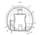
- FIG. 3A is a diagram illustrating a change in the position of an input terminal provided in the support portion
- FIG. 3A shows the support portion in which the input terminal is positioned at the retracted position
- FIG. 3C shows the support part in which the input terminal is located at the protruding position.
- FIG. 3A is a right view of an indoor antenna
- FIG. 1B is a rear view of an indoor antenna. It is the II-II sectional view taken on the line shown to FIG. 1B.
- FIG. 3A is a diagram illustrating a change in the position of an input terminal provided in the support portion
- FIG. 3A shows the support portion in which the input terminal is positioned at the retracted position
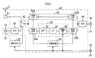
- FIG. 5 is a block diagram illustrating a first modification of the circuit configuration illustrated in FIG. 4.
- FIG. 5 is a block diagram illustrating a second modification of the circuit configuration illustrated in FIG. 4.
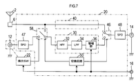
- FIG. 6 is a block diagram illustrating a third modification of the circuit configuration illustrated in FIG. 4.
- SYMBOLS 1 ... Indoor antenna, 2 ... Antenna element, 4 ... Support part, 4a ... Opening part, 5 ... Cover body, 6 ... Antenna terminal, 8 ... Protective case, 10 ... Wall part, 12 ... Input terminal, 12a ... Connector part, DESCRIPTION OF SYMBOLS 14 ... Output terminal, 14a ... Connector part, 16 ... Power supply terminal, 20 ... Circuit board, 22 ... Detection switch, 22a ... Operation part, 30 ... Amplifier circuit, 32 ... HPF (high pass filter), 34 ... LPF (low pass filter) 36 ... amplifying unit, 40 ... pass circuit, 42 ...
- the indoor antenna 1 of the present embodiment has a hollow support portion 4 formed in a disk shape so that it can be placed on an indoor desk or shelf, and a support portion 4.
- the antenna element 2 By fixing the power feeding unit to the provided antenna terminal 6 (see FIG. 2), the antenna element 2 (FIG. 4) is electrically connected to the circuit board 20 in the support unit 4 and supported by the support unit 4.
- a protective case 8 that is fixed on the support portion 4 so as to cover the antenna element 2 and protects the antenna element 2.
- the antenna element 2 is for receiving television broadcast radio waves in the UHF band, and is composed of, for example, a loop antenna.
- the protective case 8 is formed of a synthetic resin that can transmit radio waves.
- the protective case 8 has a spherical shape in FIGS. 1A and 1B, but this shape may be any character shape or sculpture to make the indoor antenna 1 look like a figurine. It can also be formed like a work of art that has been decorated. In addition, a picture or a design can be formed on the surface of the protective case 8.
- the support part 4 is a disk shape, as shown in FIG. 2, a part of outer periphery is linear, and the input terminal 12 and the output terminal 14 are provided at both ends of the linear part. Yes.
- a power supply terminal 16 for supplying a power supply voltage (DC voltage) from the outside is provided between the terminals 12 and 14.
- the input terminal 12 and the output terminal 14 are fixed to the wall portion 10 erected so as to surround the circuit board 20 from the bottom surface of the support portion 4.
- the wall portion 10 is formed integrally with the support portion 4 from a synthetic resin, and the circuit board 20 is fixed inside the wall portion 10 while being housed in a shielding metal case 18 together with the power terminal 16. ing.
- the input terminal 12 and the output terminal 14 are respectively formed as connector portions 12a and 14a constituting an F-type connector so that a coaxial cable can be connected using an F-type plug.
- the other ends of these terminals are bent in an L shape with respect to the connector portions 12a and 14a, and are fixed to portions facing each other in the wall portion 10.
- the output terminal 14 is fixed to the wall portion 10 with the connector portion 14 a protruding from the support portion 4, and is connected to the circuit board 20 inside the wall portion 10.
- the input terminal 12 has a retracted position in which the connector portion 12a is accommodated in the support portion 4 as shown in FIG. 3A, and a protrusion in which the connector portion 12a protrudes from the support portion 4 as shown in FIG. 3C. It is fixed so as to be rotatable with respect to the wall 10 so that it can be displaced between the positions.
- the support 4 is formed with an opening 4 a for allowing the input terminal 12 to pass when the input terminal 12 is displaced from the retracted position to the protruding position or vice versa.
- the opening 4a is provided with a lid 5 for closing the opening 4a when the input terminal 12 is in the retracted position or the protruding position.
- a micro switch 22 is provided in which the operation unit 22a is opened and turned off.
- the detection switch 22 corresponds to an example of the position detection unit of the present invention, and the terminal of the detection switch 22 is connected to the circuit board 20 in the wall portion 10.
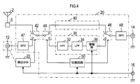
- the circuit board 20 includes an amplifier circuit 30 for amplifying a reception signal input from the antenna element 2 or the input terminal 12, and a path circuit (for passing the reception signal as it is).
- the amplifier circuit 30 passes through the high-pass filter (HPF) 32 and the low-pass filter (LPF) 34 that selectively pass the UHF band received signal (television broadcast signal) to be amplified, and both the filters 32 and 34.
- the amplifier 36 is configured to amplify the received signal, and the amplifier 36 is supplied with the power supply voltage input from the power supply terminal 16.
- an SPD surge protection device
- an SPD lightning arrester
- the passage route changeover switches 44 and 46 and the input source changeover switch 42 correspond to examples of the passage route changeover unit and the input source changeover unit of the present invention, respectively, and are manually operated by the user of the indoor antenna 1. It is also possible to use an operation switch that can switch the signal path.
- the passage path changeover switches 44 and 46 and the input source changeover switch 42 are high-frequency switches that can switch signal paths by energization / non-energization.
- the passage path changeover switches 44 and 46 are set to select the path circuit 40 as a reception signal passage path when not energized, and to select the amplifier circuit 30 as a reception signal passage path when energization is performed.
- the circuit board 20 is provided with a switching circuit 50 that receives the power supply voltage input to the power supply terminal 16 and outputs a drive signal for energization as a circuit for driving each of the path changeover switches 44 and 46. ing.
- the passage path changeover switches 44 and 46 select the path circuit 40 as the passage path of the received signal.
- the amplifier circuit 30 is selected as a reception signal passing path.
- the input source changeover switch 42 is set to pass the reception signal from the antenna element 2 when not energized and to pass the reception signal input to the input terminal 12 when energized.
- the power supply voltage input to the power supply terminal 16 is applied to the input source changeover switch 42 via the detection switch 22 that is switched on / off according to the position of the input terminal 12.
- the input source changeover switch 42 is energized when the input terminal 12 is disposed at the protruding position where the received signal can be input and the power supply voltage is input to the power supply terminal 16.
- the reception signal input to the signal is passed through the passage path changeover switch 44 to the amplifier circuit 30 side.
- the reception signal from the antenna element 2 is passed to the amplifier circuit 30 or the path circuit 40 side via the passage path changeover switch 44.
- the indoor antenna 1 of the present embodiment as an antenna device that outputs the received signal from the antenna element 2 from the output terminal 14 without being amplified by switching by the changeover switches 42 to 46.
- each of the change-over switches 42 to 46 is constituted by a high-frequency switch that can switch the path of the received signal by energization / de-energization, and when the power supply voltage is supplied to the power supply terminal 16, By energizing the passage path switching switches 44 and 46 or the input source switching switch 42 via the circuit 50 or the detection switch 22, the path of the received signal is switched.
- the user can automatically switch the path of the received signal from the path circuit 40 to the amplifier circuit 30 only by supplying a power supply voltage for driving the amplifier circuit 30 to the power supply terminal 16.
- the user simply changes the position of the input terminal 12 from the retracted position to the protruding position in order to input a received signal from the outside, when the power supply voltage is input to the power supply terminal 16 (in other words, the amplifier circuit 30).
- the reception signal input to the amplifier circuit 30 at the time of the operation can be set to the reception signal input from the input terminal 12.
- the indoor antenna 1 of the present embodiment when the operation mode of the indoor antenna 1 is set to any of the three operation modes (antenna device, antenna device with amplifier, and amplification device) described above, There is no need to perform a special operation for switching the changeover switches 42 to 46, and the usability can be improved.
- the input terminal 12 when there is no need to input a reception signal from the input terminal 12, the input terminal 12 can be closed by setting the position of the input terminal 12 to the retracted position and closing the lid 5. Can be stored in the support portion 4 to hide the connector portion 12a from the outside.
- the attenuation that includes the variable attenuator is provided as the pass circuit.
- a circuit may be provided. In this way, the received signal can be attenuated by a desired attenuation amount and passed, and the signal level of the received signal output from the output terminal 14 can be set to a more appropriate level.
- the amplifying circuit 30 may be provided with a variable attenuator to adjust the gain of the amplifying circuit 30, or an AGC circuit may be provided to automatically control the output level to a constant level. May be.
- a filter circuit including low-pass filters (hereinafter referred to as variable LPFs) 52a and 52b and high-pass filters (hereinafter referred to as variable HPFs) 54a and 54b capable of switching the cutoff frequency by energization / non-energization from the switching circuit 50 is provided. It may be.
- variable LPFs 52a and 52b that have a cutoff frequency of 300 MHz when energized and a cutoff frequency of 770 MHz when not energized, respectively.
- variable HPFs 54a and 54b are provided, each having a cutoff frequency of 470 MHz when energized and a cutoff frequency of 900 MHz when de-energized.
- variable LPFs 52 a and 52 b and the variable HPFs 54 a and 54 b are energized via the switching circuit 50.
- the variable LPFs 52a and 52b suppress the passage of the reception signal (UHF band television broadcast signal: frequency 470 MHz to 770 MHz), and the variable HPFs 54a and 54b allow the reception signal to pass.
- variable LPFs 52a and 52b and the variable HPFs 54a and 54b are in a non-energized state, so that the variable LPFs 52a and 52b receive the received signal.
- the variable HPFs 54a and 54b suppress the passage of the received signal.
- the passage path switching unit may be configured using filter circuits (variable LPFs 52a and 52b and variable HPFs 54a and 54b) that can switch the cutoff frequency by energization / non-energization.
- filter circuits variable LPFs 52a and 52b and variable HPFs 54a and 54b
- a filter circuit capable of switching the cut-off frequency by energization / non-energization
- a semiconductor element such as a PIN diode or a semiconductor switch capable of switching the passage / cutoff of a high-frequency signal by energization / non-energization
- a filter circuit capable of changing the filter characteristics by switching between energization and non-energization.
- variable LPFs 52a and 52b and the variable HPFs 54a and 54b of the first modification may be configured using this type of filter circuit. Since this type of filter circuit is well known, the description of the specific configuration of the variable LPFs 52a and 52b and the variable HPFs 54a and 54b is omitted in the first modification. (Second modification) In the first modification, the variable LPFs 52a and 52b are provided on the input side and the output side of the path circuit 40, and the variable HPFs 54a and 54b are provided on the input side and the output side of the amplifier circuit 30. Although the description has been made assuming that each filter circuit is used to switch to either the pass circuit 40 or the amplifier circuit 30, for example, as shown in FIG.
- a variable LPF 52 a is provided on the input side of the pass circuit 40 and the input of the amplifier circuit 30.
- a passage path changeover switch 56 made of a semiconductor element capable of switching passage / cutoff of a high-frequency signal by energization / non-energization is provided, and the output side of the path circuit 40 and the amplifier circuit 30 is the same as that of the above embodiment.
- a passing path switch 46 may be provided.
- the reception signal from the antenna element 2 is output to the outside via the path circuit 40 and the output terminal 14, and the power supply terminal 16 is supplied with the power supply.
- the voltage is supplied, when the detection switch 22 is in the ON state (in other words, when the input terminal 12 is in the retracted position), the received signal from the antenna element 2 is transmitted via the amplifier circuit 30 and the output terminal 14.
- the detection switch 22 is in an off state (in other words, when the input terminal 12 is in the protruding position)
- the received signal from the input terminal 12 is output to the outside through the amplifier circuit 30 and the output terminal 14. Is done.
- the path circuit 40 only needs to be able to pass the reception signal from the antenna element 2 and does not need to pass the reception signal input to the input terminal 12. Therefore, as shown in FIG. In 40, the received signal from the antenna element 2 may be inputted as it is, and a passing path changeover switch 46 may be provided on the output side.
- either the reception signal from the antenna element 2 or the reception signal from the input terminal 12 may be input to the amplifier circuit 30.
- a source changeover switch 58 may be provided.
- the input source changeover switch 58 is required to have not only a function as an input source changeover unit but also a function as a passage route changeover unit. Therefore, when the power supply voltage is not supplied from the changeover circuit 50 (non- When the power supply voltage is supplied from the switching circuit 50 (when the power is supplied), the open state is not formed as shown in FIG. Thus, the input terminal of the amplifier circuit 30 may be selectively switched to the antenna element 2 side or the input terminal 12 side.
- the reception signal from the antenna element 2 is input to the amplifier circuit 30 and the detection switch 22 is in the off state (in other words, the input terminal 12 is in the protruding position)
- the reception signal from the input terminal 12 is input to the amplifier circuit 30. It is configured to do so.
- the reception signal from the antenna element 2 is output to the outside via the path circuit 40 and the output terminal 14, and the power supply terminal 16 is supplied with the power supply.
- the voltage is supplied, when the input terminal 12 is in the retracted position, the received signal from the antenna element 2 is output to the outside through the amplifier circuit 30 and the output terminal 14, and when the input terminal 12 is in the protruding position. Since the received signal from the input terminal 12 is output to the outside via the amplifier circuit 30 and the output terminal 14, the third modified example is the same as the first embodiment and the first and second modified examples. The effect of can be obtained.
Landscapes
- Engineering & Computer Science (AREA)
- Computer Networks & Wireless Communication (AREA)
- Input Circuits Of Receivers And Coupling Of Receivers And Audio Equipment (AREA)
- Details Of Aerials (AREA)
- Support Of Aerials (AREA)
- Variable-Direction Aerials And Aerial Arrays (AREA)
Abstract
La présente invention concerne une antenne intérieure pourvue d'une partie d'antenne et d'une partie de support destinée à porter la partie d'antenne et à installer celle-ci en intérieur. La partie de support est pourvue d'une borne d'entrée, d'une borne de sortie, d'un circuit amplificateur, d'un circuit d'intercommunication, d'une unité de commutation de trajet d'intercommunication et d'une unité de commutation de source d'entrée. L'unité de commutation de trajet d'intercommunication commute le trajet d'intercommunication pour que le signal de réception passe à travers celui-ci pour atteindre la borne de sortie, soit vers un circuit amplificateur soit vers le circuit d'intercommunication. Lorsque le trajet d'intercommunication est commuté vers le circuit d'amplificateur par l'unité de commutation de trajet d'intercommunication, l'unité de commutation de source d'entrée commute la source d'entrée de l'entrée du signal de réception vers le circuit amplificateur, soit vers un élément d'antenne dans la partie d'antenne soit vers la borne d'entrée.
Applications Claiming Priority (2)
| Application Number | Priority Date | Filing Date | Title |
|---|---|---|---|
| JP2011-072983 | 2011-03-29 | ||
| JP2011072983A JP5757760B2 (ja) | 2011-03-29 | 2011-03-29 | 室内アンテナ |
Publications (1)
| Publication Number | Publication Date |
|---|---|
| WO2012133320A1 true WO2012133320A1 (fr) | 2012-10-04 |
Family
ID=46931037
Family Applications (1)
| Application Number | Title | Priority Date | Filing Date |
|---|---|---|---|
| PCT/JP2012/057768 Ceased WO2012133320A1 (fr) | 2011-03-29 | 2012-03-26 | Antenne intérieure |
Country Status (2)
| Country | Link |
|---|---|
| JP (1) | JP5757760B2 (fr) |
| WO (1) | WO2012133320A1 (fr) |
Cited By (2)
| Publication number | Priority date | Publication date | Assignee | Title |
|---|---|---|---|---|
| CN109257119A (zh) * | 2018-11-09 | 2019-01-22 | 成都九华圆通科技发展有限公司 | 一种适用于不同射频信号频段的无线电监测天线系统 |
| CN111866556A (zh) * | 2019-04-30 | 2020-10-30 | 广东中元创新科技有限公司 | 一种用于电视天线接收的信号直通和放大兼容模块 |
Citations (4)
| Publication number | Priority date | Publication date | Assignee | Title |
|---|---|---|---|---|
| JPH0249236U (fr) * | 1988-09-29 | 1990-04-05 | ||
| JPH10322261A (ja) * | 1997-05-15 | 1998-12-04 | Nec Shizuoka Ltd | 無線携帯情報端末 |
| JP2000341017A (ja) * | 1999-05-25 | 2000-12-08 | Matsushita Electric Ind Co Ltd | 携帯情報通信端末装置 |
| JP2005130442A (ja) * | 2003-09-30 | 2005-05-19 | Sharp Corp | 無線通信用回路、無線通信装置、無線通信システム |
Family Cites Families (1)
| Publication number | Priority date | Publication date | Assignee | Title |
|---|---|---|---|---|
| US20100073577A1 (en) * | 2008-09-18 | 2010-03-25 | Powerq Technologies, Inc. | Portable digital antenna |
-
2011
- 2011-03-29 JP JP2011072983A patent/JP5757760B2/ja not_active Expired - Fee Related
-
2012
- 2012-03-26 WO PCT/JP2012/057768 patent/WO2012133320A1/fr not_active Ceased
Patent Citations (4)
| Publication number | Priority date | Publication date | Assignee | Title |
|---|---|---|---|---|
| JPH0249236U (fr) * | 1988-09-29 | 1990-04-05 | ||
| JPH10322261A (ja) * | 1997-05-15 | 1998-12-04 | Nec Shizuoka Ltd | 無線携帯情報端末 |
| JP2000341017A (ja) * | 1999-05-25 | 2000-12-08 | Matsushita Electric Ind Co Ltd | 携帯情報通信端末装置 |
| JP2005130442A (ja) * | 2003-09-30 | 2005-05-19 | Sharp Corp | 無線通信用回路、無線通信装置、無線通信システム |
Cited By (4)
| Publication number | Priority date | Publication date | Assignee | Title |
|---|---|---|---|---|
| CN109257119A (zh) * | 2018-11-09 | 2019-01-22 | 成都九华圆通科技发展有限公司 | 一种适用于不同射频信号频段的无线电监测天线系统 |
| CN109257119B (zh) * | 2018-11-09 | 2024-02-27 | 成都九华圆通科技发展有限公司 | 一种适用于不同射频信号频段的无线电监测天线系统 |
| CN111866556A (zh) * | 2019-04-30 | 2020-10-30 | 广东中元创新科技有限公司 | 一种用于电视天线接收的信号直通和放大兼容模块 |
| CN111866556B (zh) * | 2019-04-30 | 2023-04-28 | 广东中元创新科技有限公司 | 一种用于电视天线接收的信号直通和放大兼容模块 |
Also Published As
| Publication number | Publication date |
|---|---|
| JP5757760B2 (ja) | 2015-07-29 |
| JP2012209704A (ja) | 2012-10-25 |
Similar Documents
| Publication | Publication Date | Title |
|---|---|---|
| US7869612B1 (en) | System and method for optimizing the strength and orientation of the inductive field of a hearing aid compatible device | |
| KR20100032333A (ko) | 스테레오 기능을 구비한 헤드폰 | |
| US20140093103A1 (en) | Increasing ground noise rejection in audio systems | |
| AU2015306927B2 (en) | Loudspeaker audio accessory for a communication device | |
| WO2005018041A3 (fr) | Capteur de champ electrique a faible bruit | |
| WO2012133320A1 (fr) | Antenne intérieure | |
| WO2006011322A1 (fr) | Système de téléphone mobile | |
| JP5222959B2 (ja) | 携帯端末 | |
| JP2008311825A (ja) | 受信装置及び中継ケーブル | |
| JP2009130812A (ja) | デュアルチャンネル放送受信機及びそれを備えた携帯端末 | |
| JP2004153310A (ja) | 無線通信装置 | |
| EP1207717A1 (fr) | Dispositif électronique avec chambre acoustique variable | |
| KR20160084984A (ko) | 고주파 스위치 | |
| CN101272001B (zh) | 接收装置和天线 | |
| KR200485782Y1 (ko) | 음원 접근 여부에 따라 동작이 제어되는 음향 장치 | |
| JP5014905B2 (ja) | 可変指向性アンテナ装置 | |
| JP2014146851A (ja) | アンテナ装置及び該アンテナ装置を備えた携帯端末 | |
| JP2014183512A (ja) | Usbケーブル | |
| JP2004023547A (ja) | 低周波減衰回路およびラジオ受信機 | |
| JP2012114547A (ja) | 送信回路 | |
| JP4479122B2 (ja) | 音声信号再生回路及びノイズキャンセリングヘッドホン回路 | |
| WO2021039061A1 (fr) | Circuit haute fréquence et dispositif de communication | |
| KR101547145B1 (ko) | 사운드 스위칭 단자가 구비된 모니터 | |
| KR102316430B1 (ko) | 위상 변위기 | |
| CN1989699A (zh) | 移动电话装置 |
Legal Events
| Date | Code | Title | Description |
|---|---|---|---|
| 121 | Ep: the epo has been informed by wipo that ep was designated in this application |
Ref document number: 12764521 Country of ref document: EP Kind code of ref document: A1 |
|
| NENP | Non-entry into the national phase |
Ref country code: DE |
|
| 122 | Ep: pct application non-entry in european phase |
Ref document number: 12764521 Country of ref document: EP Kind code of ref document: A1 |