WO2012133380A1 - Carte à circuit et son procédé de fabrication - Google Patents
Carte à circuit et son procédé de fabrication Download PDFInfo
- Publication number
- WO2012133380A1 WO2012133380A1 PCT/JP2012/057883 JP2012057883W WO2012133380A1 WO 2012133380 A1 WO2012133380 A1 WO 2012133380A1 JP 2012057883 W JP2012057883 W JP 2012057883W WO 2012133380 A1 WO2012133380 A1 WO 2012133380A1
- Authority
- WO
- WIPO (PCT)
- Prior art keywords
- wiring
- circuit board
- insulating layer
- etching
- wiring portion
- Prior art date
- Legal status (The legal status is an assumption and is not a legal conclusion. Google has not performed a legal analysis and makes no representation as to the accuracy of the status listed.)
- Ceased
Links
Images


Classifications
-
- H—ELECTRICITY
- H05—ELECTRIC TECHNIQUES NOT OTHERWISE PROVIDED FOR
- H05K—PRINTED CIRCUITS; CASINGS OR CONSTRUCTIONAL DETAILS OF ELECTRIC APPARATUS; MANUFACTURE OF ASSEMBLAGES OF ELECTRICAL COMPONENTS
- H05K1/00—Printed circuits
- H05K1/02—Details
- H05K1/0213—Electrical arrangements not otherwise provided for
- H05K1/0263—High current adaptations, e.g. printed high current conductors or using auxiliary non-printed means; Fine and coarse circuit patterns on one circuit board
- H05K1/0265—High current adaptations, e.g. printed high current conductors or using auxiliary non-printed means; Fine and coarse circuit patterns on one circuit board characterized by the lay-out of or details of the printed conductors, e.g. reinforced conductors, redundant conductors, conductors having different cross-sections
-
- H—ELECTRICITY
- H05—ELECTRIC TECHNIQUES NOT OTHERWISE PROVIDED FOR
- H05K—PRINTED CIRCUITS; CASINGS OR CONSTRUCTIONAL DETAILS OF ELECTRIC APPARATUS; MANUFACTURE OF ASSEMBLAGES OF ELECTRICAL COMPONENTS
- H05K3/00—Apparatus or processes for manufacturing printed circuits
- H05K3/02—Apparatus or processes for manufacturing printed circuits in which the conductive material is applied to the surface of the insulating support and is thereafter removed from such areas of the surface which are not intended for current conducting or shielding
- H05K3/06—Apparatus or processes for manufacturing printed circuits in which the conductive material is applied to the surface of the insulating support and is thereafter removed from such areas of the surface which are not intended for current conducting or shielding the conductive material being removed chemically or electrolytically, e.g. by photo-etch process
-
- H—ELECTRICITY
- H10—SEMICONDUCTOR DEVICES; ELECTRIC SOLID-STATE DEVICES NOT OTHERWISE PROVIDED FOR
- H10W—GENERIC PACKAGES, INTERCONNECTIONS, CONNECTORS OR OTHER CONSTRUCTIONAL DETAILS OF DEVICES COVERED BY CLASS H10
- H10W70/00—Package substrates; Interposers; Redistribution layers [RDL]
- H10W70/40—Leadframes
- H10W70/479—Leadframes on or in insulating or insulated package substrates, interposers, or redistribution layers
-
- H—ELECTRICITY
- H05—ELECTRIC TECHNIQUES NOT OTHERWISE PROVIDED FOR
- H05K—PRINTED CIRCUITS; CASINGS OR CONSTRUCTIONAL DETAILS OF ELECTRIC APPARATUS; MANUFACTURE OF ASSEMBLAGES OF ELECTRICAL COMPONENTS
- H05K1/00—Printed circuits
- H05K1/02—Details
- H05K1/0213—Electrical arrangements not otherwise provided for
- H05K1/0263—High current adaptations, e.g. printed high current conductors or using auxiliary non-printed means; Fine and coarse circuit patterns on one circuit board
-
- H—ELECTRICITY
- H05—ELECTRIC TECHNIQUES NOT OTHERWISE PROVIDED FOR
- H05K—PRINTED CIRCUITS; CASINGS OR CONSTRUCTIONAL DETAILS OF ELECTRIC APPARATUS; MANUFACTURE OF ASSEMBLAGES OF ELECTRICAL COMPONENTS
- H05K2201/00—Indexing scheme relating to printed circuits covered by H05K1/00
- H05K2201/10—Details of components or other objects attached to or integrated in a printed circuit board
- H05K2201/10007—Types of components
- H05K2201/10166—Transistor
-
- H—ELECTRICITY
- H05—ELECTRIC TECHNIQUES NOT OTHERWISE PROVIDED FOR
- H05K—PRINTED CIRCUITS; CASINGS OR CONSTRUCTIONAL DETAILS OF ELECTRIC APPARATUS; MANUFACTURE OF ASSEMBLAGES OF ELECTRICAL COMPONENTS
- H05K2203/00—Indexing scheme relating to apparatus or processes for manufacturing printed circuits covered by H05K3/00
- H05K2203/03—Metal processing
- H05K2203/0323—Working metal substrate or core, e.g. by etching, deforming
-
- H—ELECTRICITY
- H05—ELECTRIC TECHNIQUES NOT OTHERWISE PROVIDED FOR
- H05K—PRINTED CIRCUITS; CASINGS OR CONSTRUCTIONAL DETAILS OF ELECTRIC APPARATUS; MANUFACTURE OF ASSEMBLAGES OF ELECTRICAL COMPONENTS
- H05K2203/00—Indexing scheme relating to apparatus or processes for manufacturing printed circuits covered by H05K3/00
- H05K2203/14—Related to the order of processing steps
- H05K2203/1476—Same or similar kind of process performed in phases, e.g. coarse patterning followed by fine patterning
-
- H—ELECTRICITY
- H05—ELECTRIC TECHNIQUES NOT OTHERWISE PROVIDED FOR
- H05K—PRINTED CIRCUITS; CASINGS OR CONSTRUCTIONAL DETAILS OF ELECTRIC APPARATUS; MANUFACTURE OF ASSEMBLAGES OF ELECTRICAL COMPONENTS
- H05K3/00—Apparatus or processes for manufacturing printed circuits
- H05K3/40—Forming printed elements for providing electric connections to or between printed circuits
- H05K3/4038—Through-connections; Vertical interconnect access [VIA] connections
-
- H—ELECTRICITY
- H10—SEMICONDUCTOR DEVICES; ELECTRIC SOLID-STATE DEVICES NOT OTHERWISE PROVIDED FOR
- H10W—GENERIC PACKAGES, INTERCONNECTIONS, CONNECTORS OR OTHER CONSTRUCTIONAL DETAILS OF DEVICES COVERED BY CLASS H10
- H10W70/00—Package substrates; Interposers; Redistribution layers [RDL]
- H10W70/60—Insulating or insulated package substrates; Interposers; Redistribution layers
- H10W70/62—Insulating or insulated package substrates; Interposers; Redistribution layers characterised by their interconnections
- H10W70/63—Vias, e.g. via plugs
- H10W70/635—Through-vias
-
- H—ELECTRICITY
- H10—SEMICONDUCTOR DEVICES; ELECTRIC SOLID-STATE DEVICES NOT OTHERWISE PROVIDED FOR
- H10W—GENERIC PACKAGES, INTERCONNECTIONS, CONNECTORS OR OTHER CONSTRUCTIONAL DETAILS OF DEVICES COVERED BY CLASS H10
- H10W90/00—Package configurations
- H10W90/701—Package configurations characterised by the relative positions of pads or connectors relative to package parts
- H10W90/721—Package configurations characterised by the relative positions of pads or connectors relative to package parts of bump connectors
- H10W90/726—Package configurations characterised by the relative positions of pads or connectors relative to package parts of bump connectors between a chip and a stacked lead frame, conducting package substrate or heat sink
Definitions
- the present invention relates to a circuit board capable of handling a large current and a method for manufacturing the circuit board.
- FIG. 1 is a diagram schematically showing a circuit board described in Patent Document 1. As shown in FIG.
- conductor patterns 102 and 103 formed by etching a copper plate are provided on the upper and lower surfaces of a base 101 made of prepreg.
- through holes 105 penetrating the upper and lower surfaces are formed in the base 101, and copper plating 104 is formed on the upper and lower surfaces of the base 101 including the conductor patterns 102 and 103 and the inner surfaces of the through holes 105. Is given.
- the through-hole 105 to which the copper plating 104 is applied is a via-hole conductor that conducts the conductor patterns 102 and 103 formed on the upper and lower surfaces of the base 101.
- the conductor patterns 102 and 103 are made thick, thereby enabling to cope with a large current.
- the copper film forming the copper plating 105 contains impurities, the resistance value is higher than that of pure copper, and the copper plating 105 functioning as a via-hole conductor also hinders a large current.
- an object of the present invention is to provide a circuit board capable of handling a large current and a method for manufacturing the circuit board.
- the circuit board according to the present invention is integrally formed from an insulating layer and a conductive metal member, and a wiring portion provided in the insulating layer so that a part is exposed from each of the upper and lower surfaces of the insulating layer. And comprising.
- a part of the wiring part integrally formed from one conductive metal member is exposed from the upper and lower surfaces of the insulating layer.
- the conductive wiring pattern formed on the upper and lower surfaces of the insulating layer and the via-hole conductor that conducts the wiring pattern are integrally formed from one conductive metal member.
- the wiring pattern and the via hole conductor are formed separately, they are formed of different materials and bonded to each other, so that the resistance value increases at the bonded portion. For this reason, by integrally forming the wiring pattern and the via hole conductor from one conductive metal member, there is no bonding interface between the wiring pattern and the via hole conductor, and the resistance value of the wiring portion can be reduced. As a result, a circuit board capable of handling a large current can be obtained.
- the wiring pattern and the via-hole conductor are integrally formed, no peeling occurs at the joint portion between the wiring pattern and the via-hole conductor, so that the joining reliability can be improved.
- a position where a part of the wiring part on the upper and lower surfaces of the insulating layer is exposed may not be overlapped in the vertical direction of the insulating layer.
- the wiring portion does not have a linear shape along the vertical direction of the insulating layer, the possibility of the wiring portion coming out from the insulating layer can be reduced.
- the wiring portion has a columnar shape along the vertical direction of the insulating layer, and has a shape that swells from the upper and lower surfaces of the insulating layer toward the central portion in the vertical direction. But you can.
- the circuit board according to the present invention may have a structure in which a nickel plating film is formed on a part of the wiring portion exposed from the upper and lower surfaces of the insulating layer.
- the strength in the exposed portion can be ensured by forming the nickel plating film.
- the circuit board according to the present invention may have a configuration in which electronic components are directly mounted on a part of the wiring portion exposed from the upper surface of the insulating layer.
- the recessed portion is less likely to be formed in the exposed portion and the flatness of the exposed portion is high, so that electronic parts can be directly mounted and land formation is not required.
- the electronic component may be a power semiconductor element.
- the power semiconductor element refers to a power conversion semiconductor element or a power control semiconductor element, and is also referred to as a power semiconductor element.
- This configuration realizes a circuit board that can handle power semiconductor elements that handle high currents at high voltages.
- the electronic component may be sealed with resin.
- the electronic component can be protected by sealing with the resin.
- the method for manufacturing a circuit board according to the present invention includes a step of etching a first surface of one conductive metal member to form a wiring pattern, and the metal member is removed by etching on the first surface. A step of filling the portion with an insulator, a step of etching the second surface of the metal member to form a wiring pattern, and a portion of the second surface where the metal member has been removed by etching. And filling with.
- the insulator is filled. Therefore, even after the wiring pattern is formed on the second surface, the wiring patterns are not separated and the insulating layer and the wiring are separated. A circuit board with integrated parts can be manufactured.
- the circuit board can be adapted to a large current by preventing the resistance value of the wiring portion in the insulating layer from increasing.
- the figure which shows the circuit board of patent document 1 typically Schematic diagram of the circuit board according to the first embodiment The schematic diagram which showed the manufacturing process of the circuit board based on Embodiment 1 in order.
- Schematic diagram of a circuit board according to the second embodiment The schematic diagram which showed the manufacturing process of the circuit board based on Embodiment 2 in order.
- Schematic diagram of a circuit board according to the third embodiment The schematic diagram which showed the manufacturing process of the circuit board which concerns on Embodiment 3 in order.
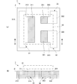
- FIG. 2 is a schematic diagram of the circuit board according to the first embodiment.
- FIG. 2A is a top view of the circuit board.
- FIG. 2B is a cross-sectional view taken along the line II-II in FIG.
- the semiconductor element 10 is mounted on the main surface (upper surface), and the semiconductor element 10 is electrically connected to an electrode such as a substrate, an element, or a ground connected to the lower surface side.
- the electronic component mounted on the circuit board 1 is the semiconductor element 10.
- the electronic component can be appropriately changed by, for example, an active element such as a silicon semiconductor element or a gallium arsenide semiconductor element, or a passive element such as a capacitor or an inductor.
- the semiconductor element 10 is a power semiconductor element, for example, a power MOSFET (Metal-Oxide-Semiconductor-Field-Effect-Transistor).
- the circuit board 1 includes an insulating layer 2 and wiring portions 31, 32 and 33.
- the insulating layer 2 is a sheet-like insulating resin, and has a rectangular parallelepiped whose upper and lower surfaces are substantially square.
- a semiconductor element 10 is mounted on the upper surface of the insulating layer 2.
- the insulating resin include an epoxy resin and a polyimide resin.
- the insulating layer 2 may be a single layer or a multilayer.
- the four surfaces adjacent to the upper and lower surfaces of the insulating layer 2 are referred to as side surfaces.
- the wiring portions 31, 32, and 33 electrically connect the semiconductor element 10 mounted on the upper surface of the insulating layer 2 and the electrode connected to the lower surface of the insulating layer 2. More specifically, the wiring part 31 is a wiring for the gate terminal of the semiconductor element 10, the wiring part 32 is a wiring for the source terminal, and the wiring part 33 is a wiring for the drain terminal.
- the wiring portions 31, 32, and 33 are each formed from one copper plate.
- conductive wiring patterns formed on the upper and lower surfaces of the insulating layer 2 are made conductive by via-hole conductors formed by filling a resin composition in which metal powder is dispersed in through holes provided in the insulating layer 2.
- the wiring pattern and the via hole conductor are formed as a wiring portion 31, 32, 33 by one copper plate.
- the resistance value of the wiring path is increased by joining the wiring patterns of different substances and the via-hole conductors, but the resistance values of the wiring parts 31, 32, and 33 are large because there is no bonding part. Don't be.
- the wiring parts 31, 32, and 33 are formed from one copper plate, the ratio of the metal component is higher than when a resin composition in which metal powder is dispersed is used, and the wiring parts 31, 32, and 33 are used. Its own resistance value is small.
- the wiring unit 31 includes an upper wiring unit 311, a lower wiring unit 312, and an interlayer connection unit 313.
- the upper wiring part 311 has a rectangular parallelepiped whose surfaces are rectangular. Two opposing surfaces forming the maximum area of the rectangular parallelepiped are defined as upper and lower surfaces.
- the upper wiring portion 311 is provided so that the longitudinal direction of the rectangular parallelepiped is parallel to one side surface of the insulating layer 2 and the upper surface is exposed from the upper surface of the insulating layer 2.
- a nickel plating film is formed on the upper surface of the upper wiring portion 311 exposed from the upper surface of the insulating layer 2, and the gate terminal of the semiconductor element 10 is directly connected thereto. By forming the nickel plating film, the strength in the exposed part is secured.
- the lower wiring portion 312 has substantially the same shape as the upper wiring portion 311, and the length in the longitudinal direction is longer than that of the upper wiring portion 311.
- the lower wiring portion 312 is provided at a position where it does not overlap the upper wiring portion 311 in the vertical direction (thickness direction) of the insulating layer 2 so that the lower surface is exposed from the lower surface of the insulating layer 2.
- the lower surface of the lower wiring portion 312 exposed from the lower surface of the insulating layer 2 is connected to an electrode such as a substrate.
- the interlayer connection part 313 is a rectangular parallelepiped flat plate parallel to the planar direction of the insulating layer 2 (the direction perpendicular to the thickness direction).
- the interlayer connection portion 313 has a longitudinal direction that coincides with the longitudinal direction of the upper wiring portion 311 and the lower wiring portion 312, one of the two parallel side surfaces is at the lower portion of the upper wiring portion 311, and the other is the upper portion of the lower wiring portion 312. Is connected to each.
- the wiring part 31 since the upper wiring part 311, the lower wiring part 312 and the interlayer connection part 313 are integrally formed from one copper plate, the wiring part 31 has no joint part of different substances in the middle and has a large resistance value. It is prevented from becoming. Further, the upper wiring portion 311 and the lower wiring portion 312 are not overlapped in the vertical direction, and are not linear in the vertical direction of the insulating layer 2, thereby preventing the wiring portion 31 from easily falling off the insulating layer 2. is doing.
- each of the upper wiring portion 311, the lower wiring portion 312 and the interlayer connection portion 313 constituting the wiring portion 31 into a prismatic shape (cuboid shape), the total volume is reduced in comparison with the case where the cylindrical portion is formed. Since it can be enlarged, the resistance value of the wiring part 31 can be reduced. Moreover, although mentioned later, since the wiring part 31 is formed by an etching from a copper plate, adjustment of the magnitude
- the wiring unit 32 includes an upper wiring unit 321, a lower wiring unit 322, and an interlayer connection unit 323.
- the upper wiring portion 321 is connected to the source terminal of the semiconductor element 10, and the lower wiring portion 322 is electrically connected to an electrode such as a substrate.
- the wiring part 33 includes an upper wiring part 331, a lower wiring part 332, and an interlayer connection part 333.
- the upper wiring portion 331 is connected to the drain terminal of the semiconductor element 10, and the lower wiring portion 332 is electrically connected to an electrode such as a substrate.
- These wiring parts 32 and 33 have the same configuration as that of the wiring part 31 although the sizes are different, and thus the description thereof is omitted.
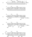
- FIG. 3 is a schematic diagram sequentially illustrating the manufacturing process of the circuit board 1 according to the first embodiment.
- FIG. 3 shows a cross section taken along line II-II of FIG. 2A in the manufacturing process.
- a photosensitive resist film is attached to the upper and lower surfaces of a copper plate (metal member) 30 having a thickness of 400 ⁇ m, and a subtractive method (a method in which unnecessary portions are removed and a circuit is left) is used. Etching is performed by exposure and development so that a rectangular pattern having a thickness of 200 ⁇ m remains. The patterns left by etching become upper wiring portions 311, 321, 331.
- the insulating resin 21 is filled into the portion removed by etching on the upper surface of the copper plate 30. At this time, the insulating resin 21 is filled so that at least the upper surface of the pattern (such as the upper wiring portion 311) remaining by etching is exposed.
- the insulating resin 21 is, for example, a polyimide resin, and after filling, the insulating resin 21 is pressed and cured.
- the third step (FIG. 3C) exposure and development are performed so that a rectangular pattern with a thickness of 100 ⁇ m remains on the lower surface of the copper plate 30, and etching is performed.
- the pattern left by etching becomes the lower wiring portions 312, 322, and 332.
- a photosensitive resist film is attached to the portion of the copper plate 30 exposed in the third step, and the pattern (upper wiring portion 311 and lower wiring) formed in the first and second steps. Then, exposure, development and etching are performed so that a pattern having a thickness of 100 ⁇ m connecting the portions 312 and the like remains. The pattern thus formed becomes interlayer connection portions 313, 323, and 333.
- the insulating resin 22 is filled into the portion removed by etching on the lower surface of the copper plate 30. At this time, the insulating resin 22 is filled so that at least the lower surface of the pattern (such as the lower wiring portion 312) left by etching is exposed.
- the insulating resin 22 is, for example, a polyimide resin, and after filling, the insulating resin 22 is pressed and cured. These insulating resins 21 and 22 become the insulating layer 2 shown in FIG.
- the circuit board 1 having the wiring portions 31, 32, 33 which are integrally formed from one copper plate and the upper wiring portion, the lower wiring portion and the interlayer connection portion are not peeled off is manufactured. be able to.
- the insulating resin 21 is filled and cured, so that the upper wiring in the manufacturing process. The parts 311, 321 and 331 can be prevented from separating.
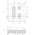
- FIG. 4 is a diagram illustrating another example of the circuit board 1 according to the first embodiment.
- the interlayer connection portions 313, 323, and 333 have a thickness of 100 ⁇ m, but may have a thickness of, for example, 200 ⁇ m to cope with a larger current.
- the wiring board according to the second embodiment is different from the wiring parts 31, 32, and 33 of the circuit board 1 according to the first embodiment in the wiring part.
- the upper wiring portion 311 and the lower wiring portion 312, the upper wiring portion 321 and the lower wiring portion 322, and the upper wiring portion 331 and the lower wiring portion 332 are each an insulating layer. 2 is formed so as not to overlap in the vertical direction.
- a part of the insulating layer 2 is formed so as to overlap the vertical direction.
- FIG. 5 is a schematic diagram of a circuit board according to the second embodiment.
- FIG. 5A is a top view of the circuit board.
- FIG. 5B is a cross-sectional view taken along the line VV in FIG.
- the circuit board 1 according to the second embodiment includes an insulating layer 2 and wiring portions 41, 42, and 43.
- the insulating layer 2 is the same as that in the first embodiment.
- the wiring portions 41, 42, and 43 are each formed from one copper plate, as in the first embodiment.
- the wiring part 41 includes an upper wiring part 411 and a lower wiring part 412.
- the upper wiring part 411 is provided in the insulating layer 2 similarly to the upper wiring part 311 of the first embodiment.
- the lower wiring portion 412 has substantially the same shape as the upper wiring portion 411, and the length in the longitudinal direction is longer than that of the upper wiring portion 311.
- the lower wiring portion 412 is provided such that a part of the upper surface is connected to a part of the lower surface of the upper wiring portion 411 and the lower surface is exposed from the lower surface of the insulating layer 2. That is, as shown in FIG. 5A, the lower wiring portion 412 partially overlaps with the upper wiring portion 411 when viewed from the upper surface.
- the wiring part 41 since the upper wiring part 411 and the lower wiring part 412 are integrally formed from one copper plate, the wiring part 41 has no joint part of different substances on the way, and prevents the resistance value from increasing. ing. Further, since the upper wiring portion 411 and the lower wiring portion 412 are partially overlapped in the vertical direction, the interlayer connection portion 313 according to the first embodiment is not necessary, and the circuit board 1 can cope with a larger current. It becomes possible. Further, since the upper wiring portion 411 and the lower wiring portion 412 do not completely overlap in the vertical direction, the wiring portion 41 does not easily fall out of the insulating layer 2.
- the wiring part 42 includes an upper wiring part 421 and a lower wiring part 422.
- the upper wiring portion 421 is connected to the source terminal of the semiconductor element 10, and the lower wiring portion 422 is electrically connected to an electrode such as a substrate.
- the wiring part 43 includes an upper wiring part 431 and a lower wiring part 432.
- the upper wiring portion 431 is connected to the drain terminal of the semiconductor element 10, and the lower wiring portion 432 is electrically connected to an electrode such as a substrate.
- These wiring parts 42 and 43 have the same configuration as that of the wiring part 41 although the sizes thereof are different.
- FIGS. 6A and 6B are schematic views sequentially showing manufacturing steps of the circuit board 1 according to the second embodiment.
- FIG. 6 shows a cross section taken along line VV of FIG. 5A in the manufacturing process.
- a photosensitive resist film is attached to the upper and lower surfaces of the copper plate 40 having a thickness of 400 ⁇ m, and exposure and development are performed by a subtractive method so that a rectangular pattern having a thickness of 200 ⁇ m remains. Etching is performed. The patterns left by etching become upper wiring portions 411, 421, and 431.
- the insulating resin 21 is filled into the portion removed by etching on the upper surface of the copper plate 40. At this time, the insulating resin 21 is filled so that at least the upper surface of the pattern (such as the upper wiring portion 411) remaining after the etching is exposed.
- the insulating resin 21 is, for example, a polyimide resin, and after filling, the insulating resin 21 is pressed and cured.
- a rectangular pattern having a thickness of 200 ⁇ m is left on the lower surface of the copper plate 40 so as to overlap with a part of the lower surface of the etching (upper wiring portion 411 and the like) formed in the first step. Then, exposure and development are performed, and etching is performed. The pattern left by etching becomes the lower wiring portions 412, 422, and 432.
- the insulating resin 22 is filled into the portion removed by etching on the lower surface of the copper plate 40. At this time, the insulating resin 22 is filled so that at least the lower surface of the pattern (such as the lower wiring portion 412) left by etching is exposed.
- the insulating resin 22 is, for example, a polyimide resin, and after filling, the insulating resin 22 is pressed and cured. The insulating resins 21 and 22 become the insulating layer 2 shown in FIG.
- the circuit board 1 having the wiring portions 41, 42, 43 integrally formed from one copper plate can be manufactured.
- FIG. 7 is a diagram illustrating another example of the circuit board 1 according to the second embodiment.
- the upper wiring portion 411 (or 421,431) has a thickness of 300 ⁇ m
- the lower wiring portion 412 (or 422,432) has a thickness of 200 ⁇ m.
- the upper wiring portion 411 (or 421, 431) and the lower wiring portion 412 (or 422, 432) may partially overlap.
- the thickness of each of the upper wiring portion 411 (or 421, 431) and the lower wiring portion 412 (or 422, 432) is set to 300 ⁇ m, and in the plane direction of the insulating layer 2, The upper wiring portion 411 (or 421, 431) and the lower wiring portion 412 (or 422, 432) may partially overlap.
- the circuit board 1 since the thickness of the wiring portions 41, 42, and 43 can be increased, the circuit board 1 can be made to cope with a larger current.
- the wiring portion is formed in a column shape along the thickness direction of the insulating layer 2.
- FIG. 8 is a schematic diagram of a circuit board according to the third embodiment.
- FIG. 8A is a top view of the circuit board.
- FIG. 8B is a cross-sectional view taken along line VIII-VIII in FIG.
- the circuit board 1 according to the third embodiment includes an insulating layer 2 and wiring portions 51, 52, and 53.
- the insulating layer 2 is the same as that in the first embodiment.
- the wiring parts 51, 52, 53 are each formed from one copper plate, as in the first and second embodiments.
- the wiring parts 51, 52, and 53 have upper and lower surfaces of the same size and shape, and have a columnar shape in which the central part in the axial direction perpendicular to the upper and lower surfaces bulges outward.
- the wiring portions 51, 52, and 53 are provided in the insulating layer 2 such that the axial direction is along the thickness direction of the insulating layer 2 and the upper and lower surfaces are exposed from the upper and lower surfaces of the insulating layer 2.
- the wiring portions 51, 52, and 53 have a shape in which the central portion swells, so that it is difficult for the wiring portions 51, 52, and 53 to fall off the insulating layer 2. Moreover, in this embodiment, since the width
- FIG. 9 is a schematic diagram sequentially illustrating the manufacturing process of the circuit board 1 according to the third embodiment.
- FIG. 9 shows a cross section taken along line VIII-VIII in FIG. 8A in the manufacturing process.
- a photosensitive resist film is attached to the upper and lower surfaces of the copper plate 50 having a thickness of 400 ⁇ m, and the patterns 511 and 521 having a trapezoidal cross section are left by the subtractive method. Exposure, development, and etching. The pattern left by etching becomes the upper part of the wiring parts 51, 52, 53.
- the insulating resin 21 is filled into the portion removed by etching on the upper surface of the copper plate 50. At this time, the insulating resin 21 is filled so that at least the upper surface of the pattern left by etching is exposed.
- the insulating resin 21 is, for example, a polyimide resin, and after filling, the insulating resin 21 is pressed and cured.
- the third step (FIG. 9C) exposure, development and etching are performed so that a 200 ⁇ m thick pattern having the same shape as the pattern formed in the first step remains on the lower surface of the copper plate 50.
- the pattern left by etching becomes the lower part of the wiring parts 51, 52, 53.
- the insulating resin 22 is filled in the portion removed by etching on the lower surface of the copper plate 50. At this time, the insulating resin 22 is filled so that at least the lower surface of the pattern left by etching is exposed.
- the insulating resin 22 is, for example, a polyimide resin, and after filling, the insulating resin 22 is pressed and cured. The insulating resins 21 and 22 become the insulating layer 2 shown in FIG.
- the circuit board 1 having the wiring portions 51, 52, 53 integrally formed from one copper plate can be manufactured.
- the wiring portions 51, 52, and 53 have a columnar shape in which the central portion in the axial direction perpendicular to the upper and lower surfaces bulges outward, but the shape can be changed as appropriate.
- FIG. 10 is a diagram illustrating another example of the circuit board 1 according to the third embodiment.
- the wiring portions 51, 52, and 53 may have a rectangular parallelepiped shape.
- the wiring portions 51, 52, and 53 may have a L-shaped cross section, or as shown in FIG. The shape which becomes a shape may be sufficient.
- circuit board 1 can be changed as appropriate, and the actions and effects described in the above-described embodiment are merely a list of the most preferable actions and effects that arise from the present invention.
- the actions and effects of the invention are not limited to those described in the above embodiment.
- the semiconductor element 10 mounted on the circuit board 1 may be sealed with a thermosetting epoxy resin or the like.
- FIG. 11 is a schematic view showing a cross section of the circuit board 1 in which the semiconductor element 10 is sealed with resin. As shown in FIG. 11, the semiconductor element 10 can be protected from an environment such as heat and humidity by sealing the semiconductor element 10 with a resin.
- the wiring board may be any one of the first, second, and third embodiments, and is shown in FIG. 4, FIG. 7, and FIG.
- the wiring board 1 of the modification shown may be sufficient.
Landscapes
- Engineering & Computer Science (AREA)
- Microelectronics & Electronic Packaging (AREA)
- Manufacturing & Machinery (AREA)
- Structure Of Printed Boards (AREA)
- Manufacturing Of Printed Circuit Boards (AREA)
- Manufacturing Of Printed Wiring (AREA)
- Printing Elements For Providing Electric Connections Between Printed Circuits (AREA)
- Production Of Multi-Layered Print Wiring Board (AREA)
Abstract
L'invention concerne une carte à circuit (1) qui comporte : une plaque d'isolation (2) sur une surface de laquelle un élément semi-conducteur (10) est installé, et des sections de circuits imprimés (31, 32, 33) placées sur la couche isolante (2). Les sections de circuits imprimés (31, 32, 33) sont configurées en sections de circuits imprimés supérieures (311, 321, 331), sections de circuits imprimés inférieures (312, 322, 332) et sections de connexion intercouche (313, 323, 333). Les sections de circuits imprimés supérieures (311, 321, 331), sections de circuits imprimés inférieures (312, 322, 332) et sections de connexion intercouche (313, 323, 333) sont formées d'un seul bloc sur une plaque de cuivre. L'invention concerne ainsi ladite carte à circuit qui peut être appliquée à un courant élevé et son procédé de fabrication.
Priority Applications (2)
| Application Number | Priority Date | Filing Date | Title |
|---|---|---|---|
| JP2013507593A JPWO2012133380A1 (ja) | 2011-03-28 | 2012-03-27 | 回路基板及び回路基板の製造方法 |
| US14/037,818 US20140022750A1 (en) | 2011-03-28 | 2013-09-26 | Circuit board and method of manufacturing the same |
Applications Claiming Priority (2)
| Application Number | Priority Date | Filing Date | Title |
|---|---|---|---|
| JP2011069094 | 2011-03-28 | ||
| JP2011-069094 | 2011-03-28 |
Related Child Applications (1)
| Application Number | Title | Priority Date | Filing Date |
|---|---|---|---|
| US14/037,818 Continuation US20140022750A1 (en) | 2011-03-28 | 2013-09-26 | Circuit board and method of manufacturing the same |
Publications (1)
| Publication Number | Publication Date |
|---|---|
| WO2012133380A1 true WO2012133380A1 (fr) | 2012-10-04 |
Family
ID=46931097
Family Applications (1)
| Application Number | Title | Priority Date | Filing Date |
|---|---|---|---|
| PCT/JP2012/057883 Ceased WO2012133380A1 (fr) | 2011-03-28 | 2012-03-27 | Carte à circuit et son procédé de fabrication |
Country Status (3)
| Country | Link |
|---|---|
| US (1) | US20140022750A1 (fr) |
| JP (2) | JPWO2012133380A1 (fr) |
| WO (1) | WO2012133380A1 (fr) |
Cited By (6)
| Publication number | Priority date | Publication date | Assignee | Title |
|---|---|---|---|---|
| WO2014188964A1 (fr) * | 2013-05-22 | 2014-11-27 | 株式会社村田製作所 | Carte de câblage à composant intégré et procédé de fabrication de carte de câblage à composant intégré |
| JP2019083323A (ja) * | 2014-11-20 | 2019-05-30 | 日本精工株式会社 | 電子部品搭載用放熱基板 |
| JP2020092152A (ja) * | 2018-12-04 | 2020-06-11 | 板橋精機株式会社 | プリント基板及びその製造方法 |
| WO2021029416A1 (fr) * | 2019-08-09 | 2021-02-18 | 板橋精機株式会社 | Carte de circuit imprimé |
| JP2023543330A (ja) * | 2020-11-10 | 2023-10-13 | クゥアルコム・インコーポレイテッド | 基板間勾配相互接続構造体を備えるパッケージ |
| JP2023160173A (ja) * | 2022-04-21 | 2023-11-02 | 板橋精機株式会社 | 基板の回路の製造方法及びその回路を有する基板 |
Families Citing this family (2)
| Publication number | Priority date | Publication date | Assignee | Title |
|---|---|---|---|---|
| DE102013202291C5 (de) * | 2013-02-13 | 2026-01-15 | Adidas Ag | Dämpfungselement für Sportbekleidung und Schuh mit einem solchen Dämpfungselement |
| JP6669513B2 (ja) * | 2016-02-03 | 2020-03-18 | 富士ゼロックス株式会社 | 回路基板および回路基板の製造方法 |
Citations (3)
| Publication number | Priority date | Publication date | Assignee | Title |
|---|---|---|---|---|
| JP2002289998A (ja) * | 2001-03-23 | 2002-10-04 | Citizen Watch Co Ltd | 回路基板とその製造方法 |
| JP2006332324A (ja) * | 2005-05-26 | 2006-12-07 | Hitachi Metals Ltd | 基板接続用シートの製造方法及び基板接続用シート |
| JP2010278379A (ja) * | 2009-06-01 | 2010-12-09 | Murata Mfg Co Ltd | 配線基板およびその製造方法 |
-
2012
- 2012-03-27 WO PCT/JP2012/057883 patent/WO2012133380A1/fr not_active Ceased
- 2012-03-27 JP JP2013507593A patent/JPWO2012133380A1/ja active Pending
-
2013
- 2013-09-26 US US14/037,818 patent/US20140022750A1/en not_active Abandoned
-
2014
- 2014-03-06 JP JP2014043519A patent/JP2014135502A/ja active Pending
Patent Citations (3)
| Publication number | Priority date | Publication date | Assignee | Title |
|---|---|---|---|---|
| JP2002289998A (ja) * | 2001-03-23 | 2002-10-04 | Citizen Watch Co Ltd | 回路基板とその製造方法 |
| JP2006332324A (ja) * | 2005-05-26 | 2006-12-07 | Hitachi Metals Ltd | 基板接続用シートの製造方法及び基板接続用シート |
| JP2010278379A (ja) * | 2009-06-01 | 2010-12-09 | Murata Mfg Co Ltd | 配線基板およびその製造方法 |
Cited By (11)
| Publication number | Priority date | Publication date | Assignee | Title |
|---|---|---|---|---|
| WO2014188964A1 (fr) * | 2013-05-22 | 2014-11-27 | 株式会社村田製作所 | Carte de câblage à composant intégré et procédé de fabrication de carte de câblage à composant intégré |
| JP6075448B2 (ja) * | 2013-05-22 | 2017-02-08 | 株式会社村田製作所 | 部品内蔵配線基板および部品内蔵配線基板の製造方法 |
| JP2019083323A (ja) * | 2014-11-20 | 2019-05-30 | 日本精工株式会社 | 電子部品搭載用放熱基板 |
| JP2020092152A (ja) * | 2018-12-04 | 2020-06-11 | 板橋精機株式会社 | プリント基板及びその製造方法 |
| WO2021029416A1 (fr) * | 2019-08-09 | 2021-02-18 | 板橋精機株式会社 | Carte de circuit imprimé |
| JP2021028963A (ja) * | 2019-08-09 | 2021-02-25 | 板橋精機株式会社 | プリント基板 |
| US12232253B2 (en) | 2019-08-09 | 2025-02-18 | Itabashi Seiki Co., Ltd. | Printed circuit board |
| JP2023543330A (ja) * | 2020-11-10 | 2023-10-13 | クゥアルコム・インコーポレイテッド | 基板間勾配相互接続構造体を備えるパッケージ |
| JP7442019B2 (ja) | 2020-11-10 | 2024-03-01 | クゥアルコム・インコーポレイテッド | 基板間勾配相互接続構造体を備えるパッケージ |
| JP2023160173A (ja) * | 2022-04-21 | 2023-11-02 | 板橋精機株式会社 | 基板の回路の製造方法及びその回路を有する基板 |
| JP7807801B2 (ja) | 2022-04-21 | 2026-01-28 | 板橋精機株式会社 | 基板の回路の製造方法及びその回路を有する基板 |
Also Published As
| Publication number | Publication date |
|---|---|
| JPWO2012133380A1 (ja) | 2014-07-28 |
| JP2014135502A (ja) | 2014-07-24 |
| US20140022750A1 (en) | 2014-01-23 |
Similar Documents
| Publication | Publication Date | Title |
|---|---|---|
| JP2014135502A (ja) | 回路基板の製造方法及び回路基板 | |
| US9179549B2 (en) | Packaging substrate having embedded passive component and fabrication method thereof | |
| CN107452694B (zh) | 嵌入式封装结构 | |
| US8099865B2 (en) | Method for manufacturing a circuit board having an embedded component therein | |
| CN109074947B (zh) | 电子部件 | |
| US9899235B2 (en) | Fabrication method of packaging substrate | |
| WO2011102561A1 (fr) | Carte de circuit imprimé multicouche et procédé de fabrication associé | |
| JP6627819B2 (ja) | 電子部品およびその製造方法 | |
| CN107622953B (zh) | 封装堆迭结构的制法 | |
| US20130020572A1 (en) | Cap Chip and Reroute Layer for Stacked Microelectronic Module | |
| US9082723B2 (en) | Semiconductor package and fabrication method thereof | |
| US10141266B2 (en) | Method of fabricating semiconductor package structure | |
| JP5406322B2 (ja) | 電子部品内蔵多層配線基板及びその製造方法 | |
| CN106298728A (zh) | 封装结构及其制法 | |
| JP2019021863A (ja) | 多層基板 | |
| US10506717B2 (en) | Inductor component and method of manufacturing inductor component | |
| US9433108B2 (en) | Method of fabricating a circuit board structure having an embedded electronic element | |
| TWI566331B (zh) | 封裝模組及其基板結構 | |
| TW201722224A (zh) | 印刷電路板及其製作方法 | |
| JP5890475B2 (ja) | インダクタ内蔵部品 | |
| WO2014181509A1 (fr) | Substrat multicouche et dispositif électronique qui utilise ce dernier, ainsi que procédé permettant de fabriquer un dispositif électronique | |
| WO2012172890A1 (fr) | Carte à circuits imprimés, structure de montage de composants électroniques et procédé de fabrication d'une structure de montage de composants électroniques | |
| TWI571187B (zh) | Buried element double layer board and its making method | |
| KR102016475B1 (ko) | 반도체 패키지, 반도체 패키지의 제조 방법 및 이를 이용한 적층형 패키지 | |
| TWI632647B (zh) | 封裝製程及其所用之封裝基板 |
Legal Events
| Date | Code | Title | Description |
|---|---|---|---|
| 121 | Ep: the epo has been informed by wipo that ep was designated in this application |
Ref document number: 12764807 Country of ref document: EP Kind code of ref document: A1 |
|
| ENP | Entry into the national phase |
Ref document number: 2013507593 Country of ref document: JP Kind code of ref document: A |
|
| NENP | Non-entry into the national phase |
Ref country code: DE |
|
| 122 | Ep: pct application non-entry in european phase |
Ref document number: 12764807 Country of ref document: EP Kind code of ref document: A1 |