WO2012133448A1 - フォトダイオードアレイモジュール及びその製造方法 - Google Patents
フォトダイオードアレイモジュール及びその製造方法 Download PDFInfo
- Publication number
- WO2012133448A1 WO2012133448A1 PCT/JP2012/057994 JP2012057994W WO2012133448A1 WO 2012133448 A1 WO2012133448 A1 WO 2012133448A1 JP 2012057994 W JP2012057994 W JP 2012057994W WO 2012133448 A1 WO2012133448 A1 WO 2012133448A1
- Authority
- WO
- WIPO (PCT)
- Prior art keywords
- semiconductor substrate
- photodiode array
- photodiode
- semiconductor
- etching
- Prior art date
- Legal status (The legal status is an assumption and is not a legal conclusion. Google has not performed a legal analysis and makes no representation as to the accuracy of the status listed.)
- Ceased
Links
Images


Classifications
-
- H—ELECTRICITY
- H10—SEMICONDUCTOR DEVICES; ELECTRIC SOLID-STATE DEVICES NOT OTHERWISE PROVIDED FOR
- H10F—INORGANIC SEMICONDUCTOR DEVICES SENSITIVE TO INFRARED RADIATION, LIGHT, ELECTROMAGNETIC RADIATION OF SHORTER WAVELENGTH OR CORPUSCULAR RADIATION
- H10F39/00—Integrated devices, or assemblies of multiple devices, comprising at least one element covered by group H10F30/00, e.g. radiation detectors comprising photodiode arrays
- H10F39/10—Integrated devices
- H10F39/12—Image sensors
- H10F39/18—Complementary metal-oxide-semiconductor [CMOS] image sensors; Photodiode array image sensors
- H10F39/182—Colour image sensors
-
- H—ELECTRICITY
- H04—ELECTRIC COMMUNICATION TECHNIQUE
- H04N—PICTORIAL COMMUNICATION, e.g. TELEVISION
- H04N1/00—Scanning, transmission or reproduction of documents or the like, e.g. facsimile transmission; Details thereof
- H04N1/024—Details of scanning heads ; Means for illuminating the original
- H04N1/028—Details of scanning heads ; Means for illuminating the original for picture information pick-up
- H04N1/03—Details of scanning heads ; Means for illuminating the original for picture information pick-up with photodetectors arranged in a substantially linear array
-
- H—ELECTRICITY
- H10—SEMICONDUCTOR DEVICES; ELECTRIC SOLID-STATE DEVICES NOT OTHERWISE PROVIDED FOR
- H10F—INORGANIC SEMICONDUCTOR DEVICES SENSITIVE TO INFRARED RADIATION, LIGHT, ELECTROMAGNETIC RADIATION OF SHORTER WAVELENGTH OR CORPUSCULAR RADIATION
- H10F39/00—Integrated devices, or assemblies of multiple devices, comprising at least one element covered by group H10F30/00, e.g. radiation detectors comprising photodiode arrays
- H10F39/011—Manufacture or treatment of image sensors covered by group H10F39/12
- H10F39/021—Manufacture or treatment of image sensors covered by group H10F39/12 of image sensors having active layers comprising only Group III-V materials, e.g. GaAs, AlGaAs or InP
-
- H—ELECTRICITY
- H10—SEMICONDUCTOR DEVICES; ELECTRIC SOLID-STATE DEVICES NOT OTHERWISE PROVIDED FOR
- H10F—INORGANIC SEMICONDUCTOR DEVICES SENSITIVE TO INFRARED RADIATION, LIGHT, ELECTROMAGNETIC RADIATION OF SHORTER WAVELENGTH OR CORPUSCULAR RADIATION
- H10F39/00—Integrated devices, or assemblies of multiple devices, comprising at least one element covered by group H10F30/00, e.g. radiation detectors comprising photodiode arrays
- H10F39/80—Constructional details of image sensors
- H10F39/809—Constructional details of image sensors of hybrid image sensors
-
- H—ELECTRICITY
- H10—SEMICONDUCTOR DEVICES; ELECTRIC SOLID-STATE DEVICES NOT OTHERWISE PROVIDED FOR
- H10W—GENERIC PACKAGES, INTERCONNECTIONS, CONNECTORS OR OTHER CONSTRUCTIONAL DETAILS OF DEVICES COVERED BY CLASS H10
- H10W90/00—Package configurations
-
- H—ELECTRICITY
- H10—SEMICONDUCTOR DEVICES; ELECTRIC SOLID-STATE DEVICES NOT OTHERWISE PROVIDED FOR
- H10W—GENERIC PACKAGES, INTERCONNECTIONS, CONNECTORS OR OTHER CONSTRUCTIONAL DETAILS OF DEVICES COVERED BY CLASS H10
- H10W90/00—Package configurations
- H10W90/701—Package configurations characterised by the relative positions of pads or connectors relative to package parts
- H10W90/721—Package configurations characterised by the relative positions of pads or connectors relative to package parts of bump connectors
- H10W90/724—Package configurations characterised by the relative positions of pads or connectors relative to package parts of bump connectors between a chip and a stacked insulating package substrate, interposer or RDL
Definitions
- the present invention relates to a photodiode array module and a manufacturing method thereof.
- Patent Document 1 a CCD (Charge Coupled Device) is disposed at a position before the light to be measured is incident, and an InGaAs photodiode array is disposed at a position subsequent to the CCD, and these are bump-connected to each other.
- a structure is disclosed in which output signals from each of the channels are read out by a shift register formed in a CCD.
- Patent Document 2 discloses a structure in which two HgCdTe photodiode arrays in which it is difficult to create a long sensor with one sensor are arranged in succession.
- the two photodiode arrays are arranged so as to overlap, but it is not possible to detect images in a plurality of wavelength bands. .
- Patent Document 3 discloses a structure in which a Si-CCD is disposed at a position before the light to be measured enters and an InGaAs image sensor is disposed at a position subsequent to the CCD, and an output is taken out separately from each other. In the case of this structure, images of a plurality of wavelength bands can be detected, but it is difficult to make a module having a long size.
- the present invention has been made in view of such problems, and an object thereof is to provide a photodiode array module capable of precise measurement.
- a photodiode array module is sensitive to a first semiconductor substrate having a first photodiode array that is sensitive to light in the first wavelength band and light in the second wavelength band.
- the third semiconductor substrate has wirings respectively connected to the amplifier, and each of the wirings is electrically connected to each photodiode of the first and second photodiode arrays via a bump.
- the end of the first photodiode array adjacent to the second photodiode array is a first stage.
- the first step portion is located at a boundary between the first side surface and the second side surface along the thickness direction of the first semiconductor substrate and the first side surface and the second side surface.
- a first terrace surface facing the third semiconductor substrate wherein the first side surface is closer to the third semiconductor substrate than the second side surface, and the crystal defect density in the first side surface is Lower than the crystal defect density in the two side surfaces, an end of the second photodiode array adjacent to the first photodiode array has a second stepped portion, and the second stepped portion is A third side surface and a fourth side surface along the thickness direction of the second semiconductor substrate; and a second terrace surface located at a boundary between the third side surface and the fourth side surface and facing the third semiconductor substrate.
- the third side surface is closer to the third semiconductor substrate than the fourth side surface,
- the crystal defect density in the third side surface is lower than the crystal defect density in the fourth side surface.
- the photodiode array module of the aspect of the present invention since the crystal defect density on the first side surface of the first step portion is low, the photodiode can be brought close to this, and the third side surface of the second step portion Since the crystal defect density is low, a photodiode can be brought close to this. Therefore, the first semiconductor substrate and the second semiconductor substrate can be arranged side by side without overlapping, and both photodiodes (pixels) can be continuously arranged. In addition, since the first and second semiconductor substrates do not overlap, the occurrence of stress at the overlapping portion is suppressed, and the imaging position of incident light with respect to the first and second semiconductor substrates is set to the same position. It is also possible to perform precise measurement.
- each photodiode constituting the first photodiode array includes a first conductivity type first semiconductor region and the third semiconductor of the first semiconductor substrate.
- a first pixel region of a second conductivity type located on a surface layer side of a surface facing the substrate, and the first terrace surface from the surface facing the third semiconductor substrate of the first semiconductor substrate.
- the depth is deeper than the depth of the first pixel region of the first photodiode array, and each photodiode constituting the second photodiode array includes a second semiconductor region of a first conductivity type and the second semiconductor region.
- a second pixel region of a second conductivity type located on a surface layer side of a surface of the semiconductor substrate facing the third semiconductor substrate, and a surface of the second semiconductor substrate facing the third semiconductor substrate
- the depth of the second terrace surfaces of al is characterized by deeper than the depth of the second pixel region of the second photodiode array.
- the first side surface and the third side surface extend to a position deeper than the pixel region, the first and second pixel regions from the second side surface and the fourth side surface that exist at a deeper position than the first side surface. The influence of can be suppressed.
- the method for manufacturing a photodiode array module includes preparing a first wafer including the first semiconductor substrate having the first photodiode array, and etching the first wafer along a first etching line. Exposing the first side surface, dicing the first wafer along the deepest portion of the first etching line to expose the second side surface, and the second having the second photodiode array. Preparing a second wafer including a semiconductor substrate, etching the second wafer along a second etching line to expose the third side surface, and forming the second wafer along the deepest portion of the second etching line.
- the crystal defect density in the first side surface and the third side surface formed by etching is lower than the crystal defect density in the second side surface and the fourth side surface formed when dicing. Therefore, the influence on the first and second pixel regions from the second side surface and the fourth side surface can be suppressed, and precise measurement is possible.
- the photodiode array module According to the photodiode array module according to the aspect of the present invention, it is possible to perform precise measurement over different wavelength bands.
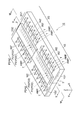
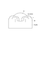
- FIG. 1 is a perspective view of a photodiode array module.
- FIG. 2 is a circuit diagram of the photodiode array module.
- FIG. 3 is a perspective view of one semiconductor substrate 2.
- FIG. 4 is a perspective view of the second semiconductor substrate 2 '.
- FIG. 5 is a cross-sectional view taken along the line VV of the photodiode array module shown in FIG.
- FIG. 6 is an enlarged view of a region VI of the photodiode array module shown in FIG.
- FIG. 7 is a cross-sectional view taken along the line VII-VII of the photodiode array module shown in FIG.
- FIG. 8 is an enlarged view of a region VIII of the photodiode array module shown in FIG.
- FIG. 1 is a perspective view of a photodiode array module.
- FIG. 2 is a circuit diagram of the photodiode array module.
- FIG. 3 is a perspective view of one semiconductor substrate 2.
- FIG. 9 is a diagram for explaining the effect of the stepped portion.
- FIG. 10 is a diagram for explaining a method of manufacturing a semiconductor substrate.
- FIG. 11 is a diagram for explaining the structure of the bump.
- FIG. 12 is a cross-sectional view of a photodiode array module in which a resin layer is interposed between substrates.
- FIG. 13 is a plan view of a wafer on which a semiconductor substrate is manufactured.
- FIG. 14 is a circuit diagram of the amplifier.
- FIG. 15 is a diagram illustrating a spectroscopic device.
- FIG. 1 is a perspective view of a photodiode array module according to an embodiment.
- the photodiode array module 10 includes a first semiconductor substrate 2 having a composition A made of a compound semiconductor material (InGaAs) and a second semiconductor substrate 2 'having a composition B made of a compound semiconductor material (InGaAs). Both the semiconductor substrates 2 and 2 ′ are placed and fixed on the third semiconductor substrate 3.
- the first semiconductor substrate 2 has a first photodiode array PDA2, and the second semiconductor substrate 2 'has a second photodiode array PDA2'.
- the structures of these semiconductor substrates 2 and 2 ' are the same except for their compositions.
- the composition A of the first semiconductor substrate 2 is sensitive to light in the first wavelength band (900 nm to 1700 nm), for example, and the composition B of the second semiconductor substrate 2 ′ is sensitive to light in the second wavelength band (900 nm to 2600 nm). However, these wavelength bands are different.
- the third semiconductor substrate 3 is made of Si.
- the surfaces of the first semiconductor substrate 2 and the second semiconductor substrate 2 ′ are bonded to the surface of the third semiconductor substrate 3.
- a plurality of amplifiers AMP to which outputs from the respective photodiodes are inputted are formed on the third semiconductor substrate 3. These amplifiers AMP are formed using a normal device forming method.
- a three-dimensional orthogonal coordinate system is set in which the thickness direction of the third semiconductor substrate 3 is the Z axis, the photodiode arrangement direction is the X axis, and the direction perpendicular to both the Z axis and the X axis is the Y axis.
- the X axis is the longitudinal direction of the semiconductor substrates 2, 2 ′, 3, and the Y axis is the width direction of the semiconductor substrates 2, 2 ′, 3.
- Light incident on the photodiode array module 10 travels in the ⁇ Z direction. That is, light enters the module 10 from the first semiconductor substrate 2 and the second semiconductor substrate 2 'side.
- the first photodiode array PDA2 and the second photodiode array PDA2 ' are located on the side of the semiconductor substrate 2, 2' facing the third semiconductor substrate 3.
- All amplifiers AMP are formed in the third semiconductor substrate 3, but these amplifiers AMP are defined by being divided into several groups.
- the first group 1G of the plurality of amplifiers AMP is a group electrically connected to the first photodiode array PDA2. That is, the first group 1G of the amplifier AMP is connected to the first wiring group W2 patterned on the third semiconductor substrate 3 and the bumps B respectively provided on the first wiring group W2.
- the photodiode array PDA2 is electrically connected to each photodiode.
- a pair of common wirings CW2 (1) and CW2 (2) (see FIG. 3) formed on the surface of the first semiconductor substrate 2 via an insulating layer extends along the X-axis, and the photodiode PD2 One pole (cathode) is configured, and the pixel region P2 configures the other pole (anode).
- a second wiring group W2 is connected to the cathode and the anode, and each photodiode is connected to the non-inverting input terminal (+) and the inverting input terminal ( ⁇ ) of the amplifier AMP (see FIG. 2).
- the second group 2G of the plurality of amplifiers AMP is a group electrically connected to the second photodiode array PDA2 '.
- the second group 2G of the amplifier AMP is connected to the second photo group via the second wiring group W2 ′ patterned on the third semiconductor substrate 3 and the bumps respectively provided on the second wiring group W2 ′.
- the photodiode array PDA2 ′ is electrically connected to each photodiode.
- a pair of common wires CW2 ′ (1) and CW2 ′ (2) (see FIG. 4) formed on the surface of the second semiconductor substrate 2 ′ via an insulating layer extends along the X axis, One pole (cathode) of the diode PD2 ′ is configured, and the pixel region P2 ′ configures the other pole (anode).
- a second wiring group W2 ′ is connected to the cathode and anode, and each photodiode is connected to the non-inverting input terminal (+) and the inverting input terminal ( ⁇ ) of the amplifier AMP (see FIG. 2). .
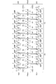
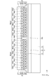
- FIG. 2 is a circuit diagram of the photodiode array module.
- the amplifier AMP is located on both sides of the photodiode arrays PDA2 and PDA2 '.
- the arrangement direction of the amplifiers AMP is parallel to the X axis, and the arrangement directions of the amplifiers AMP in both groups 1G and 2G are the same.
- the photodiodes PD2 and PD2 ' are arranged along the X axis and are located on the same straight line.
- the amplifier group located on one side is designated as 1G1 and 2G1
- the amplifier group located on the other side is designated as 1G2 and 2G2. Since the photodiode array is formed on a substrate different from the substrate on which the amplifier is formed, the amplifier does not need to be arranged on both sides of the photodiode array, and may be divided into two groups.
- FIG. 3 is a perspective view of the first semiconductor substrate 2
- FIG. 4 is a perspective view of the second semiconductor substrate 2 '.
- the first semiconductor substrate 2 and the second semiconductor substrate 2 ′ shown in FIGS. 3 and 4 are shown upside down from those shown in FIG. 1.
- 5 is a cross-sectional view taken along the line VV of the photodiode array module shown in FIG. 1
- FIG. 6 is an enlarged view of a region VI of the photodiode array module shown in FIG.
- the first semiconductor substrate 2 shown in FIG. 3 has a stepped portion STP at the end on the second photodiode array (PDA2 ') side.
- the stepped portion STP includes the first side surface S1 and the second side surface S2 along the thickness direction (Z axis) of the first semiconductor substrate 2, and the first side surface S1 and the second side surface S2.
- a terrace surface ST located at the boundary and facing the third semiconductor substrate 3 is provided.
- the front surface, the back surface, and the terrace surface ST of the first semiconductor substrate 2 are XY planes, and the first side surface S1 and the second side surface S2 are both YZ planes.
- the second semiconductor substrate 2 'shown in FIG. 4 has a stepped portion STP' at the end on the first photodiode array (PDA2) side.
- the step portion STP ′ includes the third side surface S1 ′ and the fourth side surface S2 ′ along the thickness direction (Z axis) of the second semiconductor substrate 2 ′, the third side surface S1 ′, It has a terrace surface ST ′ located at the boundary of the fourth side surface S2 ′ and facing the third semiconductor substrate 3.
- the front surface, the back surface, and the terrace surface ST 'of the second semiconductor substrate 2' are XY surfaces, and the third side surface S1 'and the fourth side surface S2' are both YZ planes.
- the first photodiode array PDA2 includes a plurality of photodiodes PD2 aligned along the X-axis direction, and the second photodiode array PDA2 ′ is also aligned along the X-axis direction.
- a plurality of photodiodes PD2 ′ are provided.
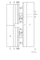
- FIG. 5 is a cross-sectional view taken along the line VV of the module shown in FIG. 1. This cross-section is precisely drawn in a zigzag manner as shown in FIGS. It is a cross section in the case of.
- FIG. 7 is a cross-sectional view taken along the arrow VII-VII of the photodiode array module shown in FIG. 1, and FIG. 8 is an enlarged view of a region VIII of the photodiode array module shown in FIG.
- the third semiconductor substrate 3 includes a semiconductor substrate 31 having a high impurity concentration, and an epitaxial layer 32 formed on the semiconductor substrate 31, and on the epitaxial layer 32 on the surface.
- An insulating layer 33 made of SiO 2 or SiN X is formed.
- wirings W2 and W2 ′ for connecting the amplifier AMP and each photodiode are patterned and formed.
- the wiring is made of aluminum or the like.
- the material / conductivity type / thickness (range) / impurity concentration (range) of each layer in the third semiconductor substrate 3 are as follows. Note that a pentavalent element (N, P, or As) can be used as an N-type impurity for Si, and a trivalent element (B or Al) can be used as a P-type impurity. A plurality of field effect transistors are formed in the epitaxial layer 32, and an amplifier AMP is formed.
- Semiconductor substrate 31 Si / P type / 200 to 800 ⁇ m / 1 ⁇ 10 16 to 1 ⁇ 10 18 cm ⁇ 3
- Epitaxial layer 32 Si / P type / 5 to 20 ⁇ m / 1 ⁇ 10 15 to 1 ⁇ 10 17 cm ⁇ 3
- the first semiconductor substrate 2 includes a semiconductor substrate 21 having a high impurity concentration, a buffer layer 22 formed on the semiconductor substrate 21, a light absorption layer 24 formed on the buffer layer 22, and a light absorption layer. 24 and a cap layer 25 formed on the substrate 24. Further, the first semiconductor substrate 2 includes a second conductivity type (P type) pixel region P ⁇ b> 2 formed in the cap layer 25 and the light absorption layer 24.
- P type second conductivity type
- An insulating layer 26 made of SiO 2 or SiN X is formed on the cap layer 25 on the surface.
- a contact electrode E21 is embedded in a contact hole provided in the insulating layer 26, and the contact electrode E21
- the patterned wiring W2 is physically and electrically connected through the bumps B.
- the wiring W2 is located on the insulating layer 33.
- the material / conductivity type / thickness (range) / impurity concentration (range) of each layer in the first semiconductor substrate 2 are as follows. Note that S or Si can be used as an N-type impurity for InGaAs or InP, and Zn can be used as a P-type impurity.
- Semiconductor substrate 21 InP / N type / 100 to 1000 ⁇ m / 1 ⁇ 10 17 to 1 ⁇ 10 20 cm ⁇ 3
- Buffer layer 22 InP / N type / 1 to 10 ⁇ m / 1 ⁇ 10 17 to 1 ⁇ 10 20 cm ⁇ 3
- Light absorbing layer 24 InGaAs / N type / 1-7 ⁇ m / 1 ⁇ 10 15 to 1 ⁇ 10 17 cm ⁇ 3
- Cap layer 25 InP / N type / 0.1 to 2 ⁇ m / 1 ⁇ 10 16 to 1 ⁇ 10 18 cm ⁇ 3
- Pixel area P2 InP / InGaAs / P type / 0.1 to 3 ⁇ m / 1 ⁇ 10 17 to 1 ⁇ 10 19 cm ⁇ 3
- Each photodiode PD2 in the first semiconductor substrate 2 is located on the surface layer side of the surface of the semiconductor regions 24, 25 facing the third semiconductor substrate 3 and the semiconductor regions 24, 25 of the first conductivity type (N type).
- a pixel region P2 made of a two-conductivity type (P-type) semiconductor.
- the plurality of pixel regions P2 are aligned along the X axis, and are intermittently arranged up to a position before reaching the end portion on the second semiconductor substrate 2 'side.
- the interface between the P-type semiconductor region P2 and the N-type semiconductor regions 24 and 25 forms a PN junction, and a depletion layer extends from the PN junction interface.
- the depletion layer In the state where no bias voltage is applied to the photodiode PD2, the depletion layer is generated by recombination of holes and electrons in the vicinity of the PN junction surface. Therefore, the size of the depletion layer supplies holes and electrons. This depends on the impurity concentration in the pixel region P 2 and the impurity concentration in the semiconductor region 24. Since the depletion layer has photosensitivity characteristics, if this depletion layer extends to a region where noise occurs, noise may be superimposed on the output of the photodiode PD2. In particular, since damage is introduced into the end portion of the first semiconductor substrate 2 on the second photodiode array side during dicing, it is preferable to suppress noise generated at such a location.
- the response speed can be improved by controlling the spread of the depletion layer and simultaneously reducing the junction capacitance defined by the depletion layer. If a non-doped layer is used between the buffer layer 22 and the light absorption layer 24, the thickness of the depletion layer is increased, so that the junction capacitance is decreased. Therefore, in this device, the response speed can be improved. It becomes possible.
- the buffer layer 22 and the semiconductor substrate 21 having an impurity concentration higher than that of the light absorption layer 24 are provided directly below the light absorption layer 24 (in the drawing, the positive direction of the Z axis is a direction directly below the first semiconductor substrate 2). Is located, and the spread of the depletion layer in the thickness direction is suppressed.
- dicing is performed using a diamond dicing blade in a region outside the depletion layer. That is, the first side surface S 1 at the end is formed by etching, and the depth of the first side surface S 1 in the Z-axis direction is deeper than the light absorption layer 24.
- the first side surface S1 reaches the buffer layer 22, but this may reach the substrate 21. Since the second side surface S2 having a high crystal defect density is located outside the depletion layer as the carrier generation region, the noise component mixed in the output signal is suppressed even if the pixel region P2 is brought close to the substrate edge. can do.
- shell cracks are likely to occur on the second side surface, and this functions as a large defect.
- the second side surface S2 is located away from the pixel region P2, the pixel region caused by the shell cracks P2 chipping and noise can also be suppressed.
- the range in which current easily flows approaches the impurity diffusion portion as the pixel region P2, and when etching is not used, depending on the size of the shell crack, the diffusion portion may be short-circuited, If a bias is applied at a very close position, the depletion layer may reach the shell crack portion.
- the terrace surface ST located at the end of the first semiconductor substrate 2 is located at the deepest part of the first side surface S1.
- the depth of the terrace surface ST from the surface of the first semiconductor substrate 2 facing the third semiconductor substrate is at least deeper than the depth of the pixel region P2 of the second photodiode array. This is because, when the depth of the terrace surface ST is shallower than the pixel region P2, the second side surface S2 having a high crystal defect density is adjacent to the side of the pixel region P2, and noise is mixed therein.
- the deeper the terrace surface ST the less the influence of noise.
- dicing is performed from a location where the influence of noise due to defects becomes small, and the substrate is removed. Disconnect.
- the crystal defect density in the first side surface S1 can be reduced by using the second side surface. It can be made lower than the crystal defect density in S2, and noise can be suppressed and the pixel region P2 can be brought close to the side surface S1.
- the closest distance from the first side surface S1 to the pixel region P2 can be set to 3 ⁇ m or more.
- the structure of the second semiconductor substrate 2 ′ is the same as that of the first semiconductor substrate 2 except for the composition.
- the text is replaced by adding “′” to the reference numeral. It is.
- the first side surface S1 and the second side surface S2 of the first semiconductor substrate 2 are the third side surface S1 ′ and the fourth side surface S2 ′ of the second semiconductor substrate 2 ′, and the terrace surface ST ′ is stepped. Constitutes part STP ′.
- the closest distance from the third side surface S1 to the pixel region P2' can be set to 3 ⁇ m or more.
- common wires CW2 (1), CW2 (2) electrically connected to N-type semiconductor regions constituting the cathode of the first photodiode array PDA2 and the cathode of the second photodiode array PDA2 ′, CW2 ′ (1) and CW2 ′ (2) include a first common line CW2 (1) and CW2 ′ (1) extending in a direction in which a plurality of the pixel regions are arranged, and a first common line CW2 (1). , CW2 ′ (1) and a second common wiring CW2 (2) CW2 ′ (2) extending in parallel.
- Insulating layers 26 and 26 ' are located on the cap layer 25, and contact electrodes E22 and E22' are embedded in the contact holes provided in the insulating layers 26 and 26 '.
- CW2 (1), CW2 (2), CW2 ′ (1), CW2 ′ (2) are connected via contact electrodes E22, E22 ′ and wirings W2, W2 ′ connected thereto via bumps B, B ′. And connected to the non-inverting input terminal (+) of the amplifier AMP (see FIG. 2).
- FIG. 8 shows a state in which the wirings W2 and W2 ′ extending from the contact electrode E21 (see FIG. 6) are located on the insulating layer 33.
- the contact electrodes E21 and E21 ′ are connected to the amplifier AMP.
- This vertical cross-sectional structure is a cross section passing through the common wirings CW2 (1) and CW2 ′ (1) (see FIGS. 3 and 4), but the common wirings CW2 (2) and CW2 ′ (2) (see FIG. 3 and FIG.
- the cross-sectional structure passing through 4) is also the same.
- the pixel regions P2 and P2 ′ are in regions between the common lines CW2 (1) and CW2 ′ (1) and the common lines CW2 (2) and CW2 ′ (2). positioned.
- the amplifier AMP is formed on the third semiconductor substrate 3.
- each group 1G, 2G of the amplifier AMP in the third semiconductor substrate 3 includes a first outer amplifier group 1G1, 2G1 and a second outer amplifier group 1G2, 2G2.
- the first outer amplifier groups 1G1 and 2G1 are located outside the region between the first and second semiconductor regions of each substrate (see FIGS. 3 and 4).
- the second outer amplifier groups 1G2 and 2G2 are located outside the region between the first and second semiconductor regions of the respective substrates.
- the first outer amplifier groups 1G1 and 2G1 are disposed closer to the common lines CW2 (1) and CW2 ′ (1) than the common lines CW2 (2) and CW2 ′ (2), and the second outer amplifier group 1G2 , 2G2 are arranged closer to the common lines CW2 (2) and CW2 ′ (2) than the common lines CW2 (1) and CW2 ′ (1).
- the pixel regions P2 and P2 ′ of each substrate are connected to one terminal ( ⁇ ) of the first outer amplifier groups 1G1 and 2G1 and the second outer amplifier groups 1G2 and 2G2 along the arrangement direction (X axis). Alternately, they are electrically connected.
- the first pixel region P2 from the left in FIG. 3 is connected to the inverting terminal ( ⁇ ) of the amplifier AMP of the outer amplifier group 1G2, and the second pixel region P2 is the inverting terminal of the amplifier AMP of the outer amplifier group 1G1.
- the third pixel region P2 is connected to ( ⁇ )
- the third pixel region P2 is connected to the inverting terminal ( ⁇ ) of the amplifier AMP of the outer amplifier group 1G2
- the fourth pixel region P2 is connected to the inverting terminal of the amplifier AMP of the outer amplifier group 1G1.
- (-)It is connected to the.
- the other terminal (+) of the first outer amplifier group 1G1 and the other terminal (+) of the second outer amplifier group 1G2 are electrically connected to the common wirings CW2 (1) and CW2 (2), respectively. Yes.
- the connection between the amplifier AMP and each region of the photodiode PD2 uses a patterned wiring W2.
- the first pixel region P2 ′ from the left in FIG. 4 is connected to the inverting terminal ( ⁇ ) of the amplifier AMP of the outer amplifier group 2G2, and the second pixel region P2 ′ is the amplifier AMP of the outer amplifier group 2G1.
- the third pixel region P2 ′ is connected to the inverting terminal ( ⁇ ) of the amplifier AMP of the outer amplifier group 2G2, and the fourth pixel region P2 ′ is connected to the inverting terminal ( ⁇ ) of the outer amplifier group 2G1. It is connected to the inverting terminal ( ⁇ ) of the amplifier AMP.
- MOD (N, 2) + 1 k
- the Nth pixel area P2 'from the left is connected to the inverting terminal (-) of the amplifier AMP in the kth outer amplifier group 2Gk.
- the other terminal (+) of the first outer amplifier group 2G1 and the other terminal (+) of the second outer amplifier group 2G2 are electrically connected to the common wirings CW2 ′ (1) and CW2 ′ (2), respectively.
- a patterned wiring W2 ' is used for connection between the amplifier AMP and each region of the photodiode PD2'.
- the amplifiers AMP are located on both sides of each pixel region P2, P2 ′, so that the number of amplifiers arranged per unit length in the arrangement direction of the pixel regions P2, P2 ′ is increased. It is possible to increase the resolution by narrowing the pitch of the pixel areas P2 and P2 ′.
- the photodiode array module since the crystal defect density on the first side surface of the first stepped portion STP is low, the photodiode can be brought close to the first stepped portion STP, and the third side surface of the second stepped portion STP ′ Since the crystal defect density is low, a photodiode can be brought close to this. Accordingly, the first semiconductor substrate 2 and the second semiconductor substrate 2 ′ can be arranged side by side without overlapping, and both photodiodes (pixels) can be continuously arranged. In addition, since the first and second semiconductor substrates 2 and 2 ′ do not overlap with each other, the generation of stress at the overlapping portion is suppressed, and the incident light is not coupled to the first and second semiconductor substrates 2 and 2 ′. Since the image position can be set to the same position, precise measurement is possible.
- the outputs of all the amplifiers AMP can be taken out from the terminals T.
- Each terminal T is connected to a circuit (shift register) that converts parallel outputs from a plurality of terminals T into serial outputs.
- a capacitor C is interposed between the input and output terminals of each amplifier AMP, and the output charge can be converted into a voltage. That is, the amplifier AMP is a charge amplifier, the amplifier AMP is an operational amplifier, and the two input terminals are virtually short-circuited. Accordingly, each of the photodiodes PD2 and PD2 'can be driven with zero bias, and an excessive spread of the depletion layer can be suppressed.
- the operational amplifier various types such as those using CMOS can be used.
- FIG. 14 is a circuit diagram showing an example of the amplifier AMP.
- the anode of the photodiode PD (PD2, PD2 ') is connected to the inverting input terminal (-), and the cathode is connected to the non-inverting input terminal (+).
- a P-channel field effect transistor PMOS and an N-channel field effect transistor NMOS are connected as shown in the figure, an operational amplifier is formed.
- a power supply line Vdd and a ground potential are connected to the operational amplifier, and an NMOS (3) adjacent to the ground potential.
- a bias potential Vbias is applied to the gate of the NMOS (4) and functions as a constant current source.
- the potential difference generated between both ends of the photodiode PF is detected by a differential pair (NMOS (1), NMOS (2)), and from the current mirror circuit (PMOS (1), PMOS (2)) from the other transistor. Large current is supplied, and the input potential difference is transmitted to the amplifier circuits (PMOS (3) and PMOS (4)) in the subsequent stage, amplified and output from the terminal T.
- a method for manufacturing the photodiode, amplifier and capacitor is as follows. A normal method may be used.
- the first photodiode array PDA2 and the second photodiode array PDA2 ′ formed thereon are , It has sensitivity to incident light in different wavelength bands.
- the above-mentioned composition A of InGaAs is In 0.53 Ga 0.47 As, and the composition B is In 0.82 Ga 0.18 As.
- the distance t2 from the back surface of the semiconductor substrate 2, 2 ′ to the pixel regions P2, P2 ′ is shorter than the distance t1 from the back surface to the front surface of the third semiconductor substrate 3, and the semiconductor substrate 2
- the light incident from the 2 ′ side passes through the semiconductor substrates 2 and 2 ′ and is sufficiently incident on the depletion layer near the pixel regions P2 and P2 ′.
- the photodiodes PD2 and PD2 ′ of the photodiode arrays PDA2 and PDA2 ′ are connected to the amplifier AMP, the outputs of the photodiodes PD2 and PD2 ′ are amplified and output to the outside. .
- the outputs of the photodiodes of the semiconductor substrates 2 and 2 ′ are input to the amplifiers AMP of the groups 1G and 2G via the bumps (B and B ′) and the wiring groups W2 and W2 ′, and are transmitted via these amplifiers AMP.
- the end portions of the semiconductor substrates 2 and 2 ′ have stepped portions STP and STP ′.
- the step portions STP and STP ′ include side surfaces S1 and S1 ′ close to the third semiconductor substrate 3 and side surfaces S2 and S2 ′ far from the third semiconductor substrate 3, but the crystal defect density of the side surfaces S1 and S1 ′. Is relatively low, the adverse effects on the photodiode arrays PDA2 and PDA2 ′ are reduced.
- FIG. 9 is a diagram for explaining the effect of the stepped portion of the first semiconductor substrate 2. This effect is the same for the step portion of the second semiconductor substrate 2 '.
- FIG. 9A dicing is performed after etching to a deep position.
- a large amount of crystal defects are introduced into the side surface S2 as indicated by the arrow D, but this is a position outside the depletion layer, and the influence on the pixel region P2 is slight.
- FIG. 9B when etching is not performed, as shown in FIG. 9B, a large amount of crystal defects are introduced in the entire side surface as indicated by an arrow D, which is caused by the crystal defects.
- noise is mixed into the pixel region P2 close to the side surface.
- a plurality of amplifiers AMP are formed and bonded to the third semiconductor substrate 3 and the third semiconductor substrate 3 made of a semiconductor material.
- First and second semiconductor substrates 2 and 2 'made of a semiconductor material are prepared.
- the buffer layer 22, the light absorption layer 24, and the cap layer 25 are sequentially grown on the semiconductor substrate 21.
- a metal organic chemical vapor deposition (MOCVD) method can be used.
- MOCVD metal organic chemical vapor deposition
- the buffer layer 22 ′, the light absorption layer 24 ′, and the cap layer 25 ′ are sequentially grown on the semiconductor substrate 21 ′.
- MOCVD metal organic chemical vapor deposition
- As a source gas for growing InP or InGaAs trimethylindium (TMI), trimethylgallium (TMGa), or trimethylarsine (TMAs) can be used.
- second conductive type (P-type) pixel regions P2 and P2 ′ located on the surface layer side of the surface of the semiconductor substrates 2 and 2 ′ facing the third semiconductor substrate 3 are formed, and the photodiode arrays PDA2 and PDA2 are formed.
- 'Form That is, by using a photolithography technique, P-type impurities are diffused into the pixel formation scheduled region, thereby forming pixel regions P2 and P2 'as anodes.
- wirings W2 and W2 ′ for connecting the contact electrodes E21, E22, E21 ′ and E22 ′ and the input terminals ( ⁇ , +) of the amplifier AMP are patterned on the third semiconductor substrate 3 with aluminum or the like,
- the semiconductor substrate 2, 2 ′ on which the diode array is formed is completed.
- Each electrode on the cathode side is connected using a common wiring.
- the wiring groups W2 and W2 ′ are formed on the third semiconductor substrate 3 via the insulating layer 33, so that each pixel region of the first photodiode array PDA2 and the amplifier AMP are connected via the wiring group W2.
- the first group 1G is electrically connected
- the wiring group W2 ′ and the second group 2G of the amplifier AMP are electrically connected. That is, the third semiconductor substrate 3 and the semiconductor substrates 2 and 2 ′ are bonded together, the photodiode arrays PDA2 and PDA2 ′ are disposed on the wiring groups W2 and W2 ′ via the bumps B and B ′, and the wiring group W2 is disposed.
- W2 ′ and each of the pixel regions P2 and P2 ′ of the photodiode are electrically connected.
- This wafer W separates the semiconductor substrate 2 or 2 'shown in FIG. 1 from the wafer by performing etching and dicing after forming each element.
- this etching and dicing as shown in FIG. 13, the longitudinal direction (X axis) of the semiconductor substrate 2 or 2 ′ is diced along the dicing lines DL10 to DL15, and the short direction (Y axis) is the semiconductor.
- Etching lines EL1, EL2, and EL3 are set only at locations where the substrates 2 and 2 ′ are adjacent, and dicing lines DL1 to DL3 are set so as to overlap the etching lines EL1, EL2, and EL3.
- dicing is performed by setting the dicing lines DL1 to DL3 along these lines, thereby forming the stepped portion.
- a dicing line DL0 in the Y-axis direction can be set separately.
- FIG. 10 is a diagram illustrating a step of forming a step portion of the first semiconductor substrate 2.
- the step of forming the step portion of the second semiconductor substrate 2 ' is the same as this.
- the resist R is applied to the surface of the wafer including the first semiconductor substrate 2, and exposure and development are performed so that the resist R is opened along the etching line (FIG. 10A). As a result, a line-shaped opening H1 is formed in the resist R.
- the insulating film 26 on the surface is etched using the resist R as a mask (FIG. 10B). This etching may be wet etching using a hydrofluoric acid aqueous solution or dry etching using a chlorine-based etching gas. Here, wet etching is used for etching.
- the compound semiconductor is etched using the resist R and the insulating film 26 as a mask.
- the wafer including the first semiconductor substrate 2 is etched to a position deeper than the depth of the pixel region P2 of the second photodiode array until it reaches the buffer layer 22 in this example (FIG. 10C).
- wet etching is used for etching.
- the InP etching solution for example, a mixed solution of hydrochloric acid and phosphoric acid, or a commonly used etching solution such as a hydrochloric acid aqueous solution, a odorous acid-based etching solution, or bromomethanol can be used.
- etching solution for InGaAs or InGaAsP for example, a citric acid-based etching solution (a mixed solution of citric acid, hydrogen peroxide, and water) or a sulfuric acid-based etching solution (a mixed solution of sulfuric acid, hydrogen peroxide, and water) is usually used.
- the etchant used can be used.
- an etching groove defined by the opening H ⁇ b> 1 is formed including one side surface (S ⁇ b> 1) of the first semiconductor substrate 2.
- the first semiconductor substrate 2 is separated from the wafer by dicing the deepest portion of the etching groove along the dicing line (FIG. 10D). Dicing is performed halfway through the semiconductor substrate 21. At the time of separation, the semiconductor substrate is attached to an expanded tape and stretched to perform separation. Of course, dicing is performed up to the back surface of the substrate. Also good.
- the first side surface S1 shown in FIG. 6 is a surface formed by etching the first semiconductor substrate 2 in the thickness direction, and the second side surface S2 is diced in the thickness direction. It is the surface formed by this.
- the crystal defect density in the side surface that appears by etching is smaller than the crystal defect density in the side surface that appears by dicing.
- the method includes the steps of preparing a first wafer including a first semiconductor substrate 2 having a first photodiode array, and etching the first wafer along first etching lines EL1, EL2, EL3 to form a first side surface S1.
- a second wafer including a second semiconductor substrate 2 ′ having a second photodiode array is prepared, and the second wafer is etched along the second etching lines EL1, EL2, EL3.
- a step of exposing the third side surface S1 ′ and a step of dicing the second wafer along the deepest portion of the second etching lines EL1, EL2, EL3 to expose the fourth side surface S2 ′ are included.
- the first semiconductor substrate 2 and the second semiconductor substrate 2 ′ are bonded to the third semiconductor substrate 3 via the bumps B and B ′, and the first semiconductor substrate 2 and the second semiconductor substrate 2 are bonded.
- the step of electrically connecting each photodiode in “to each of the amplifiers AMP via bumps B and B ′ is provided.
- the first semiconductor substrate 2 is separated from the wafer by dicing the deepest portion of the etching groove.
- the crystal defect density in the side surface S1 (see FIG. 6) that appears by etching is smaller than the crystal defect density in the side surface S2 (see FIG. 6) that appears by dicing. Since the photodiode (pixel region P2) located at the end of the first semiconductor substrate 2 is not affected by noise and does not need to be removed, a reduction in the number of photodiodes can be suppressed. In this method, the influence on the first and second pixel regions from the second side surface and the fourth side surface can be suppressed, and precise measurement is possible.
- FIG. 11 is a diagram showing the structure in the vicinity of the bump.
- An insulating layer 26 is formed on the semiconductor region P2 (or the cap layer 25).
- a contact hole is formed in the insulating layer 26, and a contact electrode E21 (or E22) is formed inside.
- a resin layer J made of photosensitive polyimide or the like is interposed between the contact electrode (under bump metal) E21 (or E22) and the bump B.
- the resin layer J can suppress disconnection and electric field concentration near the bump B.
- the bumps are made of a solder material, and the contact electrodes are made of a metal such as Ti, Pt, or Au.
- the bump B is provided not only on the first semiconductor substrate but also on the wiring formed on the third semiconductor substrate 3, and a pair of bumps is provided. The bumps are melted and bonded while facing each other. This structure is the same in the vicinity of the contact hole in the semiconductor region P2 'of the second semiconductor substrate 2'.
- FIG. 12 is a cross-sectional view of a photodiode array module having a resin layer.
- the photodiode array module further includes a resin layer RG interposed between the third semiconductor substrate 3 and the first and second semiconductor substrates 2 and 2 '.
- the adhesive strength between the third semiconductor substrate 3 and the semiconductor substrates 2, 2 ' can be increased.
- the manufacturing method further includes a step of interposing a resin layer RG between the third semiconductor substrate 3 and the semiconductor substrates 2 and 2 ′, so that the adhesive strength between the semiconductor substrate 3 and the semiconductor substrates 2 and 2 ′ is increased.
- the resin layer RG may be introduced between the substrates before bonding the substrates, or may be introduced after bonding.
- An epoxy resin can be used as the resin material.
- the crystal defect density in the side surface that appears by etching is smaller than the crystal defect density in the side surface that appears by dicing. Since it is not necessary to remove the photodiodes located at the end portions of the semiconductor substrates 2 and 2 ', it is possible to suppress a decrease in the number of photodiodes. Further, since the pitch of the light receiving portions of the third semiconductor substrate 3 and the semiconductor substrates 2 and 2 'is constant and continuous, a continuous spectrum can be obtained by combining this with this spectroscope.
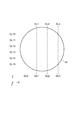
- FIG. 15 is a diagram showing a spectroscopic device using the photodiode array module described above.
- a specific wavelength band is selectively transmitted to the light incident surface side of the semiconductor substrate 2 having a photodiode having a sensitivity of 1.3 ⁇ m band and the semiconductor substrate 2 ′ having a photodiode having a sensitivity of 2.3 m band.
- a filter F2 is provided.
- a transmission wavelength variable filter (LVF: Linear Variable Filter) whose transmission wavelength band changes linearly in the length direction can be used.
- the light to be detected is split by the filter F2, and the split light is detected by each photodiode array formed on the semiconductor substrates 2 and 2 ′ and output to the outside through an amplifier formed on the semiconductor substrate 3.
- the cathode is taken out by opening a contact hole in the insulating layer formed on the cap layer and contacting the contact electrode directly with the cap layer.
- the diffusion layer may be formed after opening the contact hole, or the cap layer may be removed by etching and connected to the light absorption layer by a bump.
- a diffusion layer may be formed, or the buffer layer and the semiconductor substrate may be etched and directly connected.
- the photodiode array formed on the first and second semiconductor substrates is connected to the amplifier by connecting the anode of the photodiode to the inverting input ( ⁇ ) of the amplifier and the non-inverting input (+) of the cathode to the common wiring CW2 (1).
- CW2 (2) Connected to CW2 (2) and in the form of a differential amplifier, this is just an example.
- the common wires CW2 (1), CW2 (2), CW2 '(1), and CW2' (2) may be connected to an external power source.
- the photodiode array may be a single amplifier instead of a differential amplifier.
- the single amplifier has an advantage that a bias voltage (reverse bias voltage) can be applied to the photodiode, and the differential amplifier has an advantage that the photodiode can be zero bias.
- the amplifier is a charge amplifier having a capacity between the inverting input and the output. For resetting, it is preferable to provide a transistor as a reset switch in parallel with the capacity. Further, although the output from the amplifier is taken out from the terminal T, a switch for determining whether or not to connect the output to the terminal T may be provided between the amplifier output and the terminal T.
- SYMBOLS 3 DESCRIPTION OF SYMBOLS 3 ... 3rd semiconductor substrate, 2 ... 1st semiconductor substrate, 2 '... 2nd semiconductor substrate, PD2, PD2' ... Photodiode, P2, P2 '... Pixel region, STP, STP' ... Step part, S1 ... 1st Side surface, S2 ... second side surface, S1 '... third side surface, S2' ... fourth side surface.
Landscapes
- Engineering & Computer Science (AREA)
- Multimedia (AREA)
- Signal Processing (AREA)
- Solid State Image Pick-Up Elements (AREA)
- Light Receiving Elements (AREA)
- Facsimile Heads (AREA)
Abstract
このフォトダイオードアレイモジュールは、第1波長帯域の光に感応する第1フォトダイオードアレイを有する第1半導体基板2と、第2波長帯域の光に感応する第2フォトダイオードアレイを有する第2半導体基板2'と、複数のアンプAMPが形成されると共に第1及び第2半導体基板2,2'が重なることなく横に並べ、各フォトダイオードをバンプを介してアンプAMPに接続した第3半導体基板3とを備えている。第1半導体基板2及び第2半導体基板2'の隣接する端部には、段差部が形成されており、これにより各画素を双方の基板に渡って連続して整列させた場合においても、低ノイズで計測ができるようになる。
Description
本発明は、フォトダイオードアレイモジュール及びその製造方法に関する。
特許文献1には、被測定光が入射する前段位置にCCD(電荷結合素子)を配置すると共に、このCCDの後段位置にInGaAsフォトダイオードアレイを配置し、これらをバンプ接続し、InGaAsフォトダイオードアレイの各チャンネルからの出力信号をCCDに形成したシフトレジスタで読み出す構造が開示されている。
特許文献2には、1つのセンサで長尺センサを作成することが困難なHgCdTeのフォトダイオードアレイを、2つ連続して配置した構造が開示されている。この構造では、フォトダイオードアレイの境目で画素ピッチが変わるのを防止するため、2つのフォトダイオードアレイの一部が重なるように配置されているが、複数の波長帯域のイメージを検出することはできない。
特許文献3には、被測定光が入射する前段位置にSi-CCD、このCCDの後段位置にInGaAsイメージセンサを配置し、夫々別に外部に出力を取出す構造が開示されている。この構造の場合、複数の波長帯域のイメージを検出することができるが、寸法の長いモジュールとすることは難しい。
そこで、Si-CCDとInGaAsイメージセンサを横に並べて配置する構造が考えられるが、この場合には、双方イメージセンサの画素を、これらの境界においても連続させることは困難である。なぜならば、双方のイメージセンサの端部には、ダイシング時のイメージセンサの損傷の影響を抑制するためのマージンをとる必要があるからである。もちろん、特許文献2に記載の構造のように、一部分を重ね合わせることで、かかる不具合を解消することも可能であると考えられるが、実際には、重ね合わせ部分に応力が生じて破損が生じることや、重ね合わせの厚み分だけ入射イメージの結像位置が異なり、精密な計測ができないという不具合が発生してしまう。
したがって、異なる波長帯域を有する2つのイメージセンサを横に配置することで、連続的に画素が配列したフォトダイオードアレイモジュールを構成することは、精密な計測を行うには不向きであると考えられた。
本発明は、このような課題に鑑みてなされたものであり、精密な計測が可能なフォトダイオードアレイモジュールを提供することを目的とする。
上述の課題を解決するため、本発明の態様に係るフォトダイオードアレイモジュールは、第1波長帯域の光に感応する第1フォトダイオードアレイを有する第1半導体基板と、第2波長帯域の光に感応する第2フォトダイオードアレイを有する第2半導体基板と、複数のアンプが形成されると共に前記第1及び第2半導体基板が重なることなく横に並べて載置された第3半導体基板と、を備えるフォトダイオードアレイモジュールであって、前記第3半導体基板は前記アンプにそれぞれ接続された配線を有し、前記配線のそれぞれは、前記第1及び第2フォトダイオードアレイの各フォトダイオードにバンプを介して電気的に接続され、前記第1フォトダイオードアレイにおける、前記第2フォトダイオードアレイに隣接する端部は、第1段差部を有しており、前記第1段差部は、前記第1半導体基板の厚み方向に沿った第1側面及び第2側面と、前記第1側面及び前記第2側面の境界に位置し前記第3半導体基板に対向した第1テラス面と、を有し、前記第1側面は前記第2側面よりも、前記第3半導体基板に近く、前記第1側面内の結晶欠陥密度は、前記第2側面内の結晶欠陥密度よりも低く、前記第2フォトダイオードアレイにおける、前記第1フォトダイオードアレイに隣接する端部は、第2段差部を有しており、前記第2段差部は、前記第2半導体基板の厚み方向に沿った第3側面及び第4側面と、前記第3側面及び前記第4側面の境界に位置し前記第3半導体基板に対向した第2テラス面と、を有し、前記第3側面は前記第4側面よりも、前記第3半導体基板に近く、前記第3側面内の結晶欠陥密度は、前記第4側面内の結晶欠陥密度よりも低いことを特徴とする。
本発明の態様に係るフォトダイオードアレイモジュールによれば、第1段差部の第1側面の結晶欠陥密度が低いため、これにフォトダイオードを近接させることができ、第2段差部の第3側面の結晶欠陥密度が低いため、これにフォトダイオードを近接させることができる。したがって、第1半導体基板と第2半導体基板を重なり合うことなく横に並べて、双方のフォトダイオード(画素)を連続して配列させることが可能となる。また、第1及び第2半導体基板は、重なっていないため、重なり部分で応力が発生するのを抑制し、また、第1及び第2半導体基板に対する入射光の結像位置を、同じ位置に設定することもできるため、精密な計測が可能となる。
また、本発明の態様に係るフォトダイオードアレイモジュールにおいては、前記第1フォトダイオードアレイを構成する各フォトダイオードは、第1導電型の第1半導体領域と、前記第1半導体基板の前記第3半導体基板と対向する面の表層側に位置する第2導電型の第1画素領域と、を備えており、前記第1半導体基板の前記第3半導体基板との対向面からの前記第1テラス面の深さは、前記第1フォトダイオードアレイの前記第1画素領域の深さよりも深く、前記第2フォトダイオードアレイを構成する各フォトダイオードは、第1導電型の第2半導体領域と、前記第2半導体基板の前記第3半導体基板と対向する面の表層側に位置する第2導電型の第2画素領域と、を備えており、前記第2半導体基板の前記第3半導体基板との対向面からの前記第2テラス面の深さは、前記第2フォトダイオードアレイの前記第2画素領域の深さよりも深いことを特徴とする。
この場合、第1側面及び第3側面が、画素領域よりも深い位置まで延びているため、これよりも更に深い位置に存在する第2側面及び第4側面からの第1及び第2画素領域への影響を抑制することができる。
また、上述のフォトダイオードアレイモジュールの製造方法は、前記第1フォトダイオードアレイを有する前記第1半導体基板を含む第1ウェハを用意する工程と、前記第1ウェハを第1エッチングラインに沿ってエッチングし前記第1側面を露出させる工程と、前記第1エッチングラインの最深部に沿って前記第1ウェハをダイシングし前記第2側面を露出させる工程と、前記第2フォトダイオードアレイを有する前記第2半導体基板を含む第2ウェハを用意する工程と、前記第2ウェハを第2エッチングラインに沿ってエッチングし前記第3側面を露出させる工程と、前記第2エッチングラインの最深部に沿って前記第2ウェハをダイシングし前記第4側面を露出させる工程と、前記第1半導体基板及び第2半導体基板を、前記バンプを介して、前記第3半導体基板に貼り付け、前記第1半導体基板及び第2半導体基板における各フォトダイオードを、前記バンプを介して前記アンプのそれぞれに電気的に接続する工程と、を備えることを特徴とする。
この場合、エッチングによって形成される第1側面及び第3側面内の結晶欠陥密度は、ダイシングをした場合に形成される第2側面および第4側面の結晶欠陥密度よりも低くなる。したがって、第2側面及び第4側面からの第1及び第2画素領域への影響を抑制することができ、精密な計測が可能となる。
本発明の態様に係るフォトダイオードアレイモジュールによれば、異なる波長帯域にわたって精密な計測を行うが可能となる。
以下、実施の形態に係るフォトダイオードアレイモジュール及びその製造方法について説明する。なお、同一要素には同一符号を用いることとし、重複する説明は省略する。
図1は、実施の形態に係るフォトダイオードアレイモジュールの斜視図である。
このフォトダイオードアレイモジュール10は、化合物半導体材料(InGaAs)からなる組成Aの第1半導体基板2と、化合物半導体材料(InGaAs)からなる組成Bの第2半導体基板2’とを備えている。双方の半導体基板2,2’は、第3半導体基板3上に載置され、固定されている。第1半導体基板2は、第1フォトダイオードアレイPDA2を有しており、第2半導体基板2’は、第2フォトダイオードアレイPDA2’を有している。これらの半導体基板2,2’の構造は、その組成を除いて同一である。
第1半導体基板2の組成Aは、例えば第1波長帯域(900nm~1700nm)の光に感応し、第2半導体基板2’の組成Bは、第2波長帯域(900nm~2600nm)の光に感応し、これらの波長帯域は異なるものである。なお、第3半導体基板3はSiからなる。
第3半導体基板3の表面には、第1半導体基板2及び第2半導体基板2’の表面が貼り合わせられている。第3半導体基板3には、各フォトダイオードからの出力が入力される複数のアンプAMPが形成されている。これらのアンプAMPは、通常のデバイス形成方法を用いて形成されている。
第3半導体基板3の厚み方向をZ軸とし、フォトダイオードの配列方向をX軸とし、Z軸及びX軸の双方に垂直な方向をY軸とする三次元直交座標系を設定する。X軸は半導体基板2,2’,3の長手方向であり、Y軸は半導体基板2,2’,3の幅方向である。フォトダイオードアレイモジュール10に入射する光は-Z方向に進行する。すなわち、第1半導体基板2及び第2半導体基板2’側からモジュール10に光が入射する。第1半導体基板2及び第2半導体基板2’の裏面側から光が入射し、その表面側に位置する光感応領域で光電変換が行われ、バンプ及び配線群を介して、出力が取り出される。この出力は、第3半導体基板3に設けられたバンプ、配線群及びアンプAMPを介して外部に取り出される。
第1フォトダイオードアレイPDA2、及び、第2フォトダイオードアレイPDA2‘は、それぞれの半導体基板2、2’における第3半導体基板3に対向する面側に位置している。
全てのアンプAMPは、第3半導体基板3内に形成されているが、これらのアンプAMPを、幾つかのグループに分けて定義する。
複数のアンプAMPの第1グループ1Gは、第1フォトダイオードアレイPDA2に電気的に接続されたグループである。すなわち、アンプAMPの第1グループ1Gは、第3半導体基板3上にパターニングされ設けられた第1配線群W2、及び、この第1配線群W2にそれぞれ設けられたバンプBを介して、第1フォトダイオードアレイPDA2の各フォトダイオードにそれぞれ電気的に接続されている。
第1半導体基板2の表面上に絶縁層を介して形成された一対の共通配線CW2(1)、CW2(2)(図3参照)は、X軸に沿って延びており、フォトダイオードPD2の一方の極(カソード)を構成し、画素領域P2は他方の極(アノード)を構成している。これらのカソード及びアノードには、第2配線群W2が接続され、フォトダイオード毎にそれぞれアンプAMPの非反転入力端子(+)及び反転入力端子(-)に接続されている(図2参照)。
同様に、複数のアンプAMPの第2グループ2Gは、第2フォトダイオードアレイPDA2’に電気的に接続されたグループである。アンプAMPの第2グループ2Gは、第3半導体基板3上にパターニングされ設けられた第2配線群W2’、及び、この第2配線群W2’にそれぞれ設けられたバンプを介して、第2フォトダイオードアレイPDA2’の各フォトダイオードにそれぞれ電気的に接続されている。
第2半導体基板2’の表面上に絶縁層を介して形成された一対の共通配線CW2’(1)、CW2’(2)(図4参照)は、X軸に沿って延びており、フォトダイオードPD2’の一方の極(カソード)を構成し、画素領域P2’は他方の極(アノード)を構成している。これらのカソード及びアノードには、第2配線群W2’が接続され、フォトダイオード毎にそれぞれアンプAMPの非反転入力端子(+)及び反転入力端子(-)に接続されている(図2参照)。
図2は、フォトダイオードアレイモジュールの回路図である。
図1及び図2を参照すると、アンプAMPは、フォトダイオードアレイPDA2,PDA2’の両側に位置している。アンプAMPの配列方向はX軸に平行であり、双方のグループ1G,2GのアンプAMPの配列方向は一致している。各フォトダイオードPD2,PD2’はX軸に沿って配列され、同一直線上に位置している。フォトダイオードPD2,PD2’の配列方向を基準として、一方の側に位置するアンプ群を1G1,2G1とし、他方の側に位置するアンプ群を1G2,2G2とする。フォトダイオードアレイはアンプの形成される基板とは異なる基板に形成されているため、アンプはフォトダイオードアレイの両側に配置される必要はなく、2つのグループに分けられればよい。
図3は、第1半導体基板2の斜視図であり、図4は、第2半導体基板2’の斜視図である。図3及び図4にそれぞれ示す第1半導体基板2及び第2半導体基板2’は、図1に示したものとは上下を反転させて示されている。また、図5は、図1に示したフォトダイオードアレイモジュールのV-V矢印断面図、図6は、図5に示したフォトダイオードアレイモジュールの領域VIの拡大図である。
図3に示す第1半導体基板2は、第2フォトダイオードアレイ(PDA2’)側の端部が段差部STPを有している。段差部STPは、図5又は図6を参照すると、第1半導体基板2の厚み方向(Z軸)に沿った第1側面S1及び第2側面S2と、第1側面S1及び第2側面S2の境界に位置し第3半導体基板3に対向したテラス面STとを有している。第1半導体基板2の表面、裏面及びテラス面STはXY面であり、第1側面S1及び第2側面S2は、共にYZ平面である。
同様に、図4に示す第2半導体基板2’は、第1フォトダイオードアレイ(PDA2)側の端部が段差部STP’を有している。段差部STP’は、図5又は図6を参照すると、第2半導体基板2’の厚み方向(Z軸)に沿った第3側面S1’及び第4側面S2’と、第3側面S1’及び第4側面S2’の境界に位置し第3半導体基板3に対向したテラス面ST’とを有している。第2半導体基板2’の表面、裏面及びテラス面ST’はXY面であり、第3側面S1’及び第4側面S2’は、共にYZ平面である。
図5に示すように、第1フォトダイオードアレイPDA2は、X軸方向に沿って整列した複数のフォトダイオードPD2を備えており、第2フォトダイオードアレイPDA2’も、X軸方向に沿って整列した複数のフォトダイオードPD2’を備えている。なお、図5は、図1に示したモジュールのV-V矢印線断面図であるが、この断面は正確には、図3及び図4に示すように、V-V矢印線をジグザグに引いた場合の断面である。
また、図7は、図1に示したフォトダイオードアレイモジュールのVII-VII矢印断面図であり、図8は、図7に示したフォトダイオードアレイモジュールの領域VIIIの拡大図である。
図5~図8を参照すると、第3半導体基板3は、不純物濃度が高濃度の半導体基板31と、半導体基板31上に形成されたエピタキシャル層32を備えており、表面のエピタキシャル層32上には、SiO2又はSiNXからなる絶縁層33が形成されている。絶縁層33上には、アンプAMPと各フォトダイオードとを接続するための配線W2、W2’がパターニングされ、形成されている。配線はアルミニウムなどから形成される。
第3半導体基板3における各層の材料/導電型/厚み(範囲)/不純物濃度(範囲)は、以下の通りである。なお、Siに対するN型の不純物としては、5価の元素(N、P又はAs)を用いることができ、P型の不純物としては、3価の元素(B又はAl)を用いることができる。エピタキシャル層32内には複数の電界効果トランジスタが形成され、アンプAMPが形成されている。
・半導体基板31:Si/P型/200~800μm/1×1016~1×1018cm-3
・エピタキシャル層32:Si/P型/5~20μm/1×1015~1×1017cm-3
・エピタキシャル層32:Si/P型/5~20μm/1×1015~1×1017cm-3
また、第1半導体基板2は、不純物濃度が高濃度の半導体基板21と、半導体基板21上に形成されたバッファ層22と、バッファ層22上に形成された光吸収層24と、光吸収層24上に形成されたキャップ層25とを有している。更に、第1半導体基板2は、キャップ層25及び光吸収層24内に形成された第2導電型(P型)の画素領域P2を備えている。
表面のキャップ層25上には、SiO2又はSiNXからなる絶縁層26が形成されており、絶縁層26に設けられたコンタクトホール内には、コンタクト電極E21が埋め込まれ、コンタクト電極E21にはパターニングされた配線W2が、バンプBを介して、物理的及び電気的に接続されている。配線W2は、絶縁層33上に位置している。
第1半導体基板2における各層の材料/導電型/厚み(範囲)/不純物濃度(範囲)は、以下の通りである。なお、InGaAs又はInPに対するN型の不純物としては、S又はSiを用いることができ、P型の不純物としては、Znを用いることができる。
・半導体基板21:InP/N型/100~1000μm/1×1017~1×1020cm-3
・バッファ層22:InP/N型/1~10μm/1×1017~1×1020cm-3
・光吸収層24:InGaAs/N型/1~7μm/1×1015~1×1017cm-3
・キャップ層25:InP/N型/0.1~2μm/1×1016~1×1018cm-3
・画素領域P2:InP/InGaAs/P型/0.1~3μm/1×1017~1×1019cm-3
・バッファ層22:InP/N型/1~10μm/1×1017~1×1020cm-3
・光吸収層24:InGaAs/N型/1~7μm/1×1015~1×1017cm-3
・キャップ層25:InP/N型/0.1~2μm/1×1016~1×1018cm-3
・画素領域P2:InP/InGaAs/P型/0.1~3μm/1×1017~1×1019cm-3
第1半導体基板2における各フォトダイオードPD2は、第1導電型(N型)の半導体領域24,25と、半導体領域24,25の第3半導体基板3に対向する面の表層側に位置する第2導電型(P型)の半導体からなる画素領域P2とを備えている。複数の画素領域P2は、X軸に沿って整列しており、第2半導体基板2’側の端部に至る手前の位置まで断続的に配列している。P型の半導体領域P2とN型の半導体領域24,25との界面はPN接合を構成しており、PN接合界面から空乏層が広がっている。
フォトダイオードPD2にバイアス電圧を印加しない状態では、空乏層は、PN接合面付近において正孔と電子が再結合することで発生しているので、空乏層の寸法は、正孔及び電子を供給する画素領域P2における不純物濃度と半導体領域24における不純物濃度に依存する。空乏層は、光感応特性を有するので、この空乏層が、ノイズの発生する領域まで広がると、フォトダイオードPD2の出力に、ノイズが重畳する虞がある。特に、第1半導体基板2における第2フォトダイオードアレイ側の端部内には、ダイシング時にダメージが導入されているため、かかる箇所において発生するノイズを抑制することが好ましい。
フォトダイオードにおいては、空乏層の広がりを制御すると同時に、当該空乏層によって規定される接合容量を低下させることで、応答速度を向上させることができる。バッファ層22と光吸収層24の間にノンドープ層を用いることにすれば、空乏層の厚みは増加するので、接合容量は低下することになり、したがって、このデバイスでは応答速度を向上させることも可能となる。
本例では、光吸収層24の直下(図面ではZ軸正方向を第1半導体基板2に関する直下方向とする)には、光吸収層24よりも高い不純物濃度を有するバッファ層22及び半導体基板21が位置しており、空乏層の厚み方向の広がりを抑制している。また、第1半導体基板2の端部において、ダイヤモンド製のダイシングブレードを使ってダイシングが行われるのは、空乏層の外側の領域である。すなわち、端部における第1側面S1は、エッチングにより形成されたものであり、この第1側面S1のZ軸方向の深さは、光吸収層24よりも深い位置に存在している。上記の例では、第1側面S1は、バッファ層22に到達しているが、これは基板21まで到達することとしてもよい。結晶欠陥密度の高い第2側面S2は、キャリア発生領域としての空乏層の外側に位置しているため、画素領域P2を基板端部に近接させたとしても、出力信号に混入するノイズ成分を抑制することができる。
特に、ダイシング時においては、第2側面にシェルクラックが入りやすく、これが大きな欠陥として機能するが、第2側面S2は画素領域P2からは離間した位置に存在するため、シェルクラックに起因する画素領域P2の欠けやノイズも抑制することができる。なお、シェルクラックが発生すると、電流が流れやすい範囲が、画素領域P2としての不純物拡散部分に近づき、エッチングを用いない場合には、シェルクラックの大きさによっては、この拡散部分とショートしたり、非常に近い位置になりバイアスをかけると空乏層がシェルクラック部分に達してしまうこともある。また、初期的にはシェルクラックと拡散領域の絶縁が保たれていても、湿度が高い環境下で水分がイオン化することで電気的にショートしやすくなり、寿命が短くなることが懸念される。一方、上記実施形態では、シェルクラックの発生位置が離間しているので、これらの不具合が抑制される。
第1半導体基板2の端部に位置するテラス面STは、第1側面S1の最深部に位置している。テラス面STの第1半導体基板2の第3半導体基板との対向面からの深さは、少なくとも第2フォトダイオードアレイの画素領域P2の深さよりも深い。テラス面STの深さが、画素領域P2よりも浅い場合には、結晶欠陥密度の高い第2側面S2が、画素領域P2の側方に隣接することとなり、ノイズが混入するからである。テラス面STは深い位置に存在するほど、ノイズの影響は少なくなるが、エッチング工程は、ダイシング工程よりも時間がかかるため、欠陥によるノイズの影響が小さくなる箇所からはダイシングを行って、基板を切断する。このように、第1側面S1は第2側面S2よりも第3半導体基板3に近い位置に存在しているが、エッチングを用いることで、第1側面S1内の結晶欠陥密度は、第2側面S2内の結晶欠陥密度よりも低くすることができ、ノイズを抑制して側面S1に画素領域P2を近接させることができるようになる。
第1側面S1から、画素領域P2までの最近接距離は、3μm以上に設定することが可能となる。
なお、第2半導体基板2’の構造は、第1半導体基板2と組成を除いて同一であり、第1半導体基板2に関する説明において、符号に「’」を付加して、文章を読み替えたものである。なお、第1半導体基板2における第1側面S1,第2側面S2は、第2半導体基板2’においては、第3側面S1’、第4側面S2’であり、これらとテラス面ST’が段差部STP’を構成している。なお、第2半導体基板2’においても、第3側面S1から、画素領域P2’までの最近接距離は、3μm以上に設定することが可能となる。
図3及び図4を参照して、第1半導体基板2及び第2半導体基板2’の構造について詳説する。
それぞれの基板において、第1フォトダイオードアレイPDA2のカソード、第2フォトダイオードアレイPDA2’のカソードを構成するN型の半導体領域に電気的に接続される共通配線CW2(1),CW2(2)、CW2’(1),CW2’(2)は、前記画素領域が複数配列されている方向に延びた第1共通配線CW2(1),CW2’(1)と、第1共通配線CW2(1),CW2’(1)に対して平行に延びた第2共通配線CW2(2)CW2’(2)とを備えている。
また、キャップ層25上には絶縁層26,26’が位置しており、絶縁層26,26’に設けられたコンタクトホール内には、コンタクト電極E22,E22’が埋め込まれており、共通配線CW2(1),CW2(2)、CW2’(1),CW2’(2)は、コンタクト電極E22、E22’及びこれにバンプB、B’を介して接続された配線W2、W2’を介して、アンプAMPの非反転入力端子(+)に接続されている(図2参照)。なお、図8には、コンタクト電極E21(図6参照)から延びた配線W2、W2’が絶縁層33上に位置している状態が示されており、コンタクト電極E21、E21’はアンプAMPの反転入力端子(-)に接続される(図2参照)。この縦断面構造は、共通配線CW2(1)、CW2’(1)(図3、図4参照)を通る断面であるが、共通配線CW2(2)、CW2’(2)(図3、図4参照)を通る断面構造も、同一である。
再び、図3及び図4を参照すると、画素領域P2、P2’は、共通配線CW2(1)、CW2’(1)と共通配線CW2(2)、CW2’(2)との間の領域に位置している。なお、アンプAMPは、第3半導体基板3に形成されている。
図1~図4を参照すると、第3半導体基板3におけるアンプAMPの各グループ1G、2Gは、第1外側アンプ群1G1,2G1と、第2外側アンプ群1G2、2G2とを備えている。第1外側アンプ群1G1,2G1は、それぞれの基板の第1及び第2半導体領域間の領域(図3、図4参照)よりも外側に位置している。同様に、第2外側アンプ群1G2,2G2は、それぞれの基板の第1及び第2半導体領域間の領域よりも外側に位置している。
第1外側アンプ群1G1,2G1は、共通配線CW2(2)、CW2’(2)よりも、共通配線CW2(1)、CW2’(1)に近い位置に配置され、第2外側アンプ群1G2,2G2は、共通配線CW2(1)、CW2’(1)よりも、共通配線CW2(2)、CW2’(2)に近い位置に配置されている。
それぞれの基板の画素領域P2、P2’は、その配列方向(X軸)に沿って、第1外側アンプ群1G1,2G1、及び第2外側アンプ群1G2,2G2の一方の端子(-)に、交互に、電気的に接続されている。
すなわち、図3の左から1番目の画素領域P2は、外側アンプ群1G2のアンプAMPの反転端子(-)に接続され、2番目の画素領域P2は、外側アンプ群1G1のアンプAMPの反転端子(-)に接続され、3番目の画素領域P2は、外側アンプ群1G2のアンプAMPの反転端子(-)に接続され、4番目の画素領域P2は、外側アンプ群1G1のアンプAMPの反転端子(-)に接続されている。MOD(N,2)+1=kとすると、左からN番目の画素領域P2は、第k外側アンプ群1GkのアンプAMPの反転端子(-)に接続されている。なお、MOD(N,2)は、Nを2で割ったときの余りを示す演算子である。
また、第1外側アンプ群1G1の他方の端子(+)及び第2外側アンプ群1G2の他方の端子(+)は、それぞれ共通配線CW2(1)、CW2(2)に電気的に接続されている。アンプAMPとフォトダイオードPD2の各領域との接続はパターニングされた配線W2を用いる。
同様に、図4の左から1番目の画素領域P2’は、外側アンプ群2G2のアンプAMPの反転端子(-)に接続され、2番目の画素領域P2’は、外側アンプ群2G1のアンプAMPの反転端子(-)に接続され、3番目の画素領域P2’は、外側アンプ群2G2のアンプAMPの反転端子(-)に接続され、4番目の画素領域P2’は、外側アンプ群2G1のアンプAMPの反転端子(-)に接続されている。MOD(N,2)+1=kとすると、左からN番目の画素領域P2’は、第k外側アンプ群2GkのアンプAMPの反転端子(-)に接続されている。
また、第1外側アンプ群2G1の他方の端子(+)及び第2外側アンプ群2G2の他方の端子(+)は、それぞれ共通配線CW2’(1)、CW2’(2)に電気的に接続されている。アンプAMPとフォトダイオードPD2’の各領域との接続はパターニングされた配線W2’を用いる。
上述の構造においては、各画素領域P2、P2’の両側にアンプAMPが位置しているので、画素領域P2、P2’の配列方向の単位長さ当たりに配置されているアンプ数を増加させることができ、画素領域P2、P2’のピッチを狭くして、分解能を上げることができる。
また、上記フォトダイオードアレイモジュールによれば、第1段差部STPの第1側面の結晶欠陥密度が低いため、これにフォトダイオードを近接させることができ、第2段差部STP’の第3側面の結晶欠陥密度が低いため、これにフォトダイオードを近接させることができる。したがって、第1半導体基板2と第2半導体基板2’を重なり合うことなく横に並べて、双方のフォトダイオード(画素)を連続して配列させることが可能となる。また、第1及び第2半導体基板2,2’は、重なっていないため、重なり部分で応力が発生するのを抑制し、また、第1及び第2半導体基板2,2’に対する入射光の結像位置を、同じ位置に設定することもできるため、精密な計測が可能となる。
また、上述の構造において、全ての各アンプAMPの出力は端子Tから取り出すことができるが、各端子Tは、複数の端子Tからのパラレル出力をシリアル出力に変換する回路(シフトレジスタ)に接続することもできる。また、図2に示すように、各アンプAMPの入出力端子間には、キャパシタCが介在しており、出力された電荷を電圧に変換することができる。すなわち、アンプAMPは、チャージアンプであり、また、アンプAMPはオペアンプであって、2つの入力端子間は仮想短絡している。したがって、各フォトダイオードPD2,PD2’は、ゼロバイアス駆動することができ、空乏層の余分な広がりを抑制することができる。オペアンプの構造としては、CMOSを用いたものなど、様々な形式のものを利用することができる。
図14は、アンプAMPの一例を示す回路図である。 上述のフォトダイオードPD(PD2,PD2’)のアノードは、反転入力端子(-)に接続されており、カソードは非反転入力端子(+)に接続されている。Pチャネルの電界効果トランジスタPMOSとNチャネルの電界効果トランジスタNMOSとを図示の如く接続するとオペアンプが構成され、オペアンプには電源ラインVddとグランド電位が接続され、グランド電位に隣接するNMOS(3)、NMOS(4)のゲートにはバイアス電位Vbiasが加えられ、定電流源として機能している。フォトダイオードPFの両端間に発生した電位差は、差動対(NMOS(1)、NMOS(2))によって検出され、カレントミラー回路(PMOS(1)、PMOS(2))から、他方のトランジスタよりも大きな電流が供給され、入力電位差が後段の増幅回路(PMOS(3)、PMOS(4)に伝達され、増幅されて端子Tより出力される。なお、フォトダイオード、アンプ及びキャパシタの製造方法は、通常の方法を用いればよい。
上記フォトダイオードアレイモジュールによれば、第1半導体基板2と、第2半導体基板2’とは、組成が異なるため、これに形成される第1フォトダイオードアレイPDA2及び第2フォトダイオードアレイPDA2’は、互いに異なる波長帯域の入射光に対して感度を有する。上述のInGaAsの組成Aは、In0.53Ga0.47Asであり、組成BはIn0.82Ga0.18Asである。
なお、図6に示すように、半導体基板2、2’の裏面から画素領域P2、P2’までの距離t2は、第3半導体基板3の裏面から表面までの距離t1よりも短く、半導体基板2、2’側から入射した光が、半導体基板2、2’を透過し、十分に画素領域P2、P2’近傍の空乏層に入射する構成となっている。
図1に示すように、フォトダイオードアレイPDA2,PDA2’の各フォトダイオードPD2,PD2’は、アンプAMPに接続されているため、フォトダイオードPD2,PD2’の出力は増幅して外部に出力される。
半導体基板2、2’のフォトダイオードの出力は、バンプ(B、B’)及び配線群W2、W2’を介して、各グループ1G、2GのアンプAMPに入力され、これらのアンプAMPを介して外部に取り出される。ここで、半導体基板2、2’の端部は、段差部STP、STP’を有している。段差部STP、STP’は、第3半導体基板3に近い側面S1、S1’と、第3半導体基板3から遠い側面S2、S2’とを備えているが、側面S1、S1’の結晶欠陥密度は相対的に低いため、フォトダイオードアレイPDA2、PDA2’に対する悪影響は少なくなる。
図9は、第1半導体基板2の段差部の効果について説明するための図である。なお、この効果は、第2半導体基板2’の段差部に関しても同様である。
第2側面S2と第2フォトダイオードアレイPDA2の最近接フォトダイオード(画素領域P2)との間を近づけても、このフォトダイオードの出力の劣化が抑制されるため、当該フォトダイオードを除去する必要がない。したがって、かかる構造において、モジュール当たりのフォトダイオード数の減少を抑制することができる。
すなわち、上述の実施形態では、図9(A)に示すように、深い位置までエッチングを行った後、ダイシングを行っている。この場合、多量の結晶欠陥は、矢印Dで示すように、側面S2内に導入されるが、ここは空乏層の外側の位置であり、画素領域P2への影響は軽微である。一方、エッチングを行わない場合には、図9(B)に示すように、多量の結晶欠陥は、矢印Dで示すように、側面の全域において、導入されることとなり、この結晶欠陥に起因して、側面に近接する画素領域P2にノイズが混入することになる。図9(C)に示すように、切断面を著しく離隔した場合、多量の結晶欠陥は矢印Dのように側面の全域に導入されるが、画素領域P2への影響は小さくなる。しかしながら、このような場合には第3半導体基板を著しく離間して配置しなくてはならず、空間的に連続的な撮像を行うことができなくなる。
次に、製造方法について説明する。
このフォトダイオードアレイモジュールの製造方法においては、まず、図1に示したように、複数のアンプAMPが形成され、半導体材料からなる第3半導体基板3と、第3半導体基板3に貼り合わせられるべき第1、2半導体材料からなる半導体基板2、2’とを用意する。
半導体基板2の製造方法は、半導体基板21上に、バッファ層22、光吸収層24、キャップ層25を順次成長させる。成長には、有機金属気相成長法(MOCVD)法を用いることができる。半導体基板2’の製造方法は、半導体基板21’上に、バッファ層22’、光吸収層24’、キャップ層25’を順次成長させる。成長には、有機金属気相成長法(MOCVD)法を用いることができる。InP又はInGaAsを成長する際の原料ガスとしては、トリメチルインジウム(TMI)、トリメチルガリウム(TMGa)、トリメチルアルシン(TMAs)を用いることができる。
しかる後、半導体基板2、2’の第3半導体基板3と対向する面の表層側に位置する第2導電型(P型)の画素領域P2、P2’を形成し、フォトダイオードアレイPDA2、PDA2’を形成する。すなわち、フォトリソグラフィー技術を用い、その画素形成予定領域内にP型の不純物を拡散し、アノードとしての画素領域P2、P2’を形成する。しかる後、CVD法によって、絶縁層26,26’をキャップ層25,25’上に形成し、これにコンタクトホールを空けて、内部にコンタクト電極E21、E22、E21’、E22’を形成する。しかる後、コンタクト電極E21、E22、E21’、E22’と、アンプAMPの入力端子(-,+)とを接続する配線W2、W2’を第3半導体基板3上にアルミニウムなどでパターニングし、フォトダイオードアレイが形成された半導体基板2、2’が完成する。カソード側の各電極は共通配線を用いて接続する。
もちろん、半導体基板2、2’は、図13に示すように、ウェハW内に複数形成されるものである。
なお、上記の如く、第3半導体基板3上に絶縁層33を介して配線群W2,W2’を形成することで、配線群W2を介して第1フォトダイオードアレイPDA2の各画素領域とアンプAMPの第1グループ1Gが電気的に接続され、配線群W2’とアンプAMPの第2グループ2Gが電気的に接続される。すなわち、第3半導体基板3と半導体基板2、2’とを貼り合わせ、配線群W2、W2’上にバンプB、B’を介して、フォトダイオードアレイPDA2,PDA2’を配置し、配線群W2、W2’とフォトダイオードの画素領域P2、P2’のそれぞれとを電気的に接続する。
このウェハWは、各素子の形成後にエッチング及びダイシングを行うことで、図1に示した半導体基板2又は2’をウェハから分離する。このエッチング及びダイシングは、図13に示すように、半導体基板2又は2’の長手方向(X軸)は、ダイシングラインDL10~DL15に沿ってダイシングを行い、短手方向(Y軸)は、半導体基板2,2’が隣接する箇所のみエッチングラインEL1,EL2,EL3を設定し、エッチングラインEL1,EL2,EL3に重ねるようにダイシングラインDL1~DL3を設定する。すなわち、エッチングラインEL1,EL2,EL3に沿ってエッチングを行った後、このラインに沿ってダイシングラインDL1~DL3を設定してダイシングを行い、段差部を形成する。隣接しない箇所については、Y軸方向のダイシングラインDL0を別途設定することができる。
図10は、第1半導体基板2の段差部の形成工程を示す図である。なお、第2半導体基板2’の段差部の形成工程もこれと同一である。
第1半導体基板2を含むウェハの表面にレジストRを塗布し、エッチングラインに沿って、レジストRが開口するように露光及び現像を行う(図10(A))。これにより、レジストRにライン状の開口H1が形成されることになる。次に、レジストRをマスクとして、表面の絶縁膜26をエッチングする(図10(B))。このエッチングは、フッ酸水溶液を用いたウエットエッチングであってもよいし、塩素系エッチングガスを用いたドライエッチングであってもよい。ここでは、エッチングにウエットエッチングを用いる。
次に、レジストR及び絶縁膜26をマスクとして、化合物半導体のエッチングを行う。このエッチングでは、第1半導体基板2を含むウェハを第2フォトダイオードアレイの画素領域P2の深さよりも深い位置まで、本例ではバッファ層22に到達するまでエッチングする(図10(C))。ここでは、エッチングにウエットエッチングを用いる。InPのエッチング液としては、例えば塩酸と燐酸の混合液、或いは、塩酸水溶液、臭酸系エッチング液、ブロムメタノール等、通常用いられるエッチング液を用いることができる。InGaAsやInGaAsPのエッチング液としては、例えばクエン酸系のエッチング液(クエン酸、過酸化水素、水の混合液)や、硫酸系エッチング液(硫酸、過酸化水素、水の混合液)など、通常用いられるエッチング液を用いることができる。これにより、開口H1で規定されるエッチング溝が、第1半導体基板2の一側面(S1)を含んで形成される。
更に、エッチング溝の最深部を、ダイシングラインに沿って、ダイシングすることで、第1半導体基板2をウェハから分離する(図10(D))。なお、ダイシングは、半導体基板21の途中まで行い、分離の際には、半導体基板をエキスパンドテープに貼り付け、これを伸ばすことで、分離を行うが、もちろん、基板裏面に至るまでダイシングを行ってもよい。
図6に示した第1側面S1は、第1半導体基板2をその厚み方向にエッチングすることによって形成された面であり、第2側面S2は、第1半導体基板2をその厚み方向にダイシングすることによって形成された面である。エッチングによって現れる側面内の結晶欠陥密度は、ダイシングによって現れる側面内の結晶欠陥密度よりも小さい。
上記方法は、第1フォトダイオードアレイを有する第1半導体基板2を含む第1ウェハを用意する工程と、第1ウェハを第1エッチングラインEL1、EL2,EL3に沿ってエッチングし第1側面S1を露出させる工程と、第1エッチングラインEL1、EL2,EL3の最深部に沿って第1ウェハをダイシングし第2側面S2を露出させる工程とを備えている。同様に、この製造方法は、第2フォトダイオードアレイを有する第2半導体基板2’を含む第2ウェハを用意する工程と、第2ウェハを第2エッチングラインEL1、EL2,EL3に沿ってエッチングし第3側面S1’を露出させる工程と、第2エッチングラインEL1、EL2,EL3の最深部に沿って第2ウェハをダイシングし第4側面S2’を露出させる工程を有している。
そして、この製造方法は、第1半導体基板2及び第2半導体基板2’を、バンプB、B’を介して、第3半導体基板3に貼り付け、第1半導体基板2及び第2半導体基板2’における各フォトダイオードを、バンプB,B’を介してアンプAMPのそれぞれに電気的に接続する工程を備えている。
この方法によれば、第1半導体基板2をエッチングした後に、そのエッチング溝の最深部をダイシングすることで、第1半導体基板2をウェハから分離している。エッチングによって現れる側面S1(図6参照)内の結晶欠陥密度は、ダイシングによって現れる側面S2(図6参照)内の結晶欠陥密度よりも小さい。第1半導体基板2の端部に位置するフォトダイオード(画素領域P2)は、ノイズの影響を受けず、取り除く必要が無いので、フォトダイオード数の減少を抑制することができる。この方法では、第2側面及び第4側面からの第1及び第2画素領域への影響を抑制することができ、精密な計測が可能となる。
図11は、バンプ近傍の構造を示す図である。
半導体領域P2(或いはキャップ層25)上には絶縁層26が形成されているが、絶縁層26にはコンタクトホールが形成され、内部にコンタクト電極E21(又はE22)が形成されている。ここで、コンタクト電極(アンダーバンプメタル)E21(又はE22)とバンプBとの間には、感光性のポリイミドなどからなる樹脂層Jが介在している。樹脂層Jにより、バンプBの近傍の断線や電界集中を抑制することができる。なお、バンプは半田材料からなり、コンタクト電極はTi、PtやAuなどの金属からなる。また、第3半導体基板と第1半導体基板の接着時においては、バンプBは、第1半導体基板のみではなく、第3半導体基板3上に形成された配線上にも設けられ、一対のバンプが対向した状態で、バンプの溶融・接着が行われる。なお、この構造は、第2半導体基板2’の半導体領域P2’のコンタクトホール近傍においても同一である。
図12は、樹脂層を備えたフォトダイオードアレイモジュールの断面図である。
また、このフォトダイオードアレイモジュールは、第3半導体基板3と第1及び第2半導体基板2、2’との間に介在する樹脂層RGを更に備えている。この場合、第3半導体基板3と半導体基板2、2’との間の接着強度を高めることができる。この場合の製法は、第3半導体基板3と半導体基板2、2’との間に樹脂層RGを介在させる工程を更に備えることとなり、半導体基板3と半導体基板2,2’間の接着強度を高めることができる。樹脂層RGは、基板の貼り合わせ前に基板間に導入してもよいが、貼り合わせ後に導入してもよい。
樹脂材料としては、エポキシ系樹脂を用いることができる。
以上のように、エッチングによって現れる側面内の結晶欠陥密度は、ダイシングによって現れる側面内の結晶欠陥密度よりも小さい。半導体基板2、2’の端部に位置するフォトダイオードは、取り除く必要が無いので、フォトダイオード数の減少を抑制することができる。また、第3半導体基板3と半導体基板2、2’の受光部のピッチは一定で連続しているため、これと分光器と組み合わせることで、連続したスペクトルを得ることができる。
図15は、上述のフォトダイオードアレイモジュールを用いた分光装置を示す図である。
1.3μm帯の感度を有するフォトダイオードを有する半導体基板2と、2.3m帯の感度を有するフォトダイオードを有する半導体基板2’の光入射面側には、特定の波長帯域を選択的に透過させるフィルタF2が設けられている。フィルタF2としては、長さ方向にリニアに透過波長帯域が変化する透過波長可変フィルタ(LVF:Linear Variable Filter)を用いることができる。被検出光は、フィルタF2によって分光され、分光された光が、半導体基板2,2’に形成された各フォトダイオードアレイで検出され、半導体基板3に形成されたアンプを介して外部に出力される。上述のモジュールを用いた場合、チップ端部のチャンネル(画素)へのリーク電流が低減するので、2つのチップ間の全てのチャネル間ギャップ(距離)を等間隔にすることができる。
なお、上述の各半導体領域における導電型を逆にしてもかまわない。また、第1及び第2半導体基板においては、カソードの取り出しは、キャップ層上に形成した絶縁層にコンタクトホールをあけて、コンタクト電極を直接キャップ層にコンタクトさせているが、コンタクト抵抗を減らすため、コンタクトホールを空けたあとに拡散層を形成してもよいし、キャップ層をエッチングで除去してバンプで光吸収層に接続してもよい。光吸収層への接続の際にコンタクト抵抗を減らすために拡散層を形成してもよいし、バッファ層や半導体基板までエッチングして、直接接続してもよい。
第1及び第2半導体基板上に形成されるフォトダイオードアレイとアンプの接続は、フォトダイオードのアノードをアンプの反転入力(-)に、カソードを非反転入力(+)と共通配線CW2(1)、CW2(2)に接続し、差動アンプの形式としているが、これもあくまでも一例にすぎない。共通配線CW2(1)、CW2(2)、CW2’(1)、CW2’(2)は外部電源に接続してもよい。また、フォトダイオードアレイで、差動アンプではなく、シングルアンプの形式としてもよい。シングルアンプの場合はフォトダイオードにバイアス電圧(逆バイアス電圧)を印加できるという利点があるし、差動アンプの場合は、フォトダイオードをゼロバイアスとできる利点がある。
また、アンプは反転入力と出力の間に容量を有するチャージアンプとなっているが、リセットのため、容量に並列にリセットスイッチとしてトランジスタを設けることが好ましい。また、アンプからの出力は端子Tから取り出すが、アンプ出力と端子Tの間に出力を端子Tに接続するしないを決めるスイッチを設けてもよい。
3…第3半導体基板、2…第1半導体基板、2’…第2半導体基板、PD2,PD2’…フォトダイオード、P2,P2’…画素領域、STP,STP’…段差部、S1…第1側面、S2…第2側面、S1’…第3側面、S2’…第4側面。
Claims (3)
- 第1波長帯域の光に感応する第1フォトダイオードアレイを有する第1半導体基板と、
第2波長帯域の光に感応する第2フォトダイオードアレイを有する第2半導体基板と、
複数のアンプが形成されると共に前記第1及び第2半導体基板が重なることなく横に並べて載置された第3半導体基板と、
を備えるフォトダイオードアレイモジュールであって、
前記第3半導体基板は前記アンプにそれぞれ接続された配線を有し、
前記配線のそれぞれは、前記第1及び第2フォトダイオードアレイの各フォトダイオードにバンプを介して電気的に接続され、
前記第1フォトダイオードアレイにおける、前記第2フォトダイオードアレイに隣接する端部は、第1段差部を有しており、
前記第1段差部は、
前記第1半導体基板の厚み方向に沿った第1側面及び第2側面と、
前記第1側面及び前記第2側面の境界に位置し前記第3半導体基板に対向した第1テラス面と、
を有し、
前記第1側面は前記第2側面よりも、前記第3半導体基板に近く、
前記第1側面内の結晶欠陥密度は、前記第2側面内の結晶欠陥密度よりも低く、
前記第2フォトダイオードアレイにおける、前記第1フォトダイオードアレイに隣接する端部は、第2段差部を有しており、
前記第2段差部は、
前記第2半導体基板の厚み方向に沿った第3側面及び第4側面と、
前記第3側面及び前記第4側面の境界に位置し前記第3半導体基板に対向した第2テラス面と、
を有し、
前記第3側面は前記第4側面よりも、前記第3半導体基板に近く、
前記第3側面内の結晶欠陥密度は、前記第4側面内の結晶欠陥密度よりも低い、
ことを特徴とするフォトダイオードアレイモジュール。 - 前記第1フォトダイオードアレイを構成する各フォトダイオードは、
第1導電型の第1半導体領域と、
前記第1半導体基板の前記第3半導体基板と対向する面の表層側に位置する第2導電型の第1画素領域と、
を備えており、
前記第1半導体基板の前記第3半導体基板との対向面からの前記第1テラス面の深さは、前記第1フォトダイオードアレイの前記第1画素領域の深さよりも深く、
前記第2フォトダイオードアレイを構成する各フォトダイオードは、
第1導電型の第2半導体領域と、
前記第2半導体基板の前記第3半導体基板と対向する面の表層側に位置する第2導電型の第2画素領域と、
を備えており、
前記第2半導体基板の前記第3半導体基板との対向面からの前記第2テラス面の深さは、前記第2フォトダイオードアレイの前記第2画素領域の深さよりも深い、
ことを特徴とする請求項1に記載のフォトダイオードアレイモジュール。 - 請求項1に記載のフォトダイオードアレイモジュールの製造方法において、
前記第1フォトダイオードアレイを有する前記第1半導体基板を含む第1ウェハを用意する工程と、
前記第1ウェハを第1エッチングラインに沿ってエッチングし前記第1側面を露出させる工程と、
前記第1エッチングラインの最深部に沿って前記第1ウェハをダイシングし前記第2側面を露出させる工程と、
前記第2フォトダイオードアレイを有する前記第2半導体基板を含む第2ウェハを用意する工程と、
前記第2ウェハを第2エッチングラインに沿ってエッチングし前記第3側面を露出させる工程と、
前記第2エッチングラインの最深部に沿って前記第2ウェハをダイシングし前記第4側面を露出させる工程と、
前記第1半導体基板及び第2半導体基板を、前記バンプを介して、前記第3半導体基板に貼り付け、前記第1半導体基板及び第2半導体基板における各フォトダイオードを、前記バンプを介して前記アンプのそれぞれに電気的に接続する工程と、
を備えることを特徴とするフォトダイオードアレイモジュールの製造方法。
Priority Applications (2)
| Application Number | Priority Date | Filing Date | Title |
|---|---|---|---|
| US14/006,506 US8994041B2 (en) | 2011-03-31 | 2012-03-27 | Photodiode array module and manufacturing method for same |
| EP12763564.7A EP2693479B1 (en) | 2011-03-31 | 2012-03-27 | Photodiode array module and manufacturing method for same |
Applications Claiming Priority (2)
| Application Number | Priority Date | Filing Date | Title |
|---|---|---|---|
| JP2011-079300 | 2011-03-31 | ||
| JP2011079300A JP5486542B2 (ja) | 2011-03-31 | 2011-03-31 | フォトダイオードアレイモジュール及びその製造方法 |
Publications (1)
| Publication Number | Publication Date |
|---|---|
| WO2012133448A1 true WO2012133448A1 (ja) | 2012-10-04 |
Family
ID=46931162
Family Applications (1)
| Application Number | Title | Priority Date | Filing Date |
|---|---|---|---|
| PCT/JP2012/057994 Ceased WO2012133448A1 (ja) | 2011-03-31 | 2012-03-27 | フォトダイオードアレイモジュール及びその製造方法 |
Country Status (5)
| Country | Link |
|---|---|
| US (1) | US8994041B2 (ja) |
| EP (1) | EP2693479B1 (ja) |
| JP (1) | JP5486542B2 (ja) |
| TW (1) | TWI552327B (ja) |
| WO (1) | WO2012133448A1 (ja) |
Cited By (1)
| Publication number | Priority date | Publication date | Assignee | Title |
|---|---|---|---|---|
| WO2022102549A1 (ja) * | 2020-11-13 | 2022-05-19 | ソニーセミコンダクタソリューションズ株式会社 | 固体撮像装置 |
Families Citing this family (7)
| Publication number | Priority date | Publication date | Assignee | Title |
|---|---|---|---|---|
| JP2016151523A (ja) * | 2015-02-18 | 2016-08-22 | 浜松ホトニクス株式会社 | 赤外線検出装置 |
| US10304806B2 (en) | 2015-07-16 | 2019-05-28 | Pezy Computing K.K. | Semiconductor device |
| JP6530664B2 (ja) * | 2015-07-22 | 2019-06-12 | ソニーセミコンダクタソリューションズ株式会社 | 撮像装置及びその製造方法 |
| WO2019211968A1 (ja) * | 2018-05-02 | 2019-11-07 | ソニーセミコンダクタソリューションズ株式会社 | 固体撮像素子および撮像装置 |
| JP7452962B2 (ja) | 2018-11-16 | 2024-03-19 | ソニーセミコンダクタソリューションズ株式会社 | 撮像装置 |
| US20220406830A1 (en) * | 2021-06-21 | 2022-12-22 | Allegro Microsystems, Llc | Photoreceiver array having microlenses |
| JP2024102768A (ja) * | 2023-01-19 | 2024-07-31 | ソニーセミコンダクタソリューションズ株式会社 | 光検出装置および光検出装置の製造方法 |
Citations (6)
| Publication number | Priority date | Publication date | Assignee | Title |
|---|---|---|---|---|
| JPH0667114A (ja) | 1992-08-18 | 1994-03-11 | Fujitsu Ltd | 固体撮像素子 |
| JPH09304182A (ja) | 1996-05-20 | 1997-11-28 | Satake Eng Co Ltd | 穀粒色彩選別機 |
| WO2000062344A1 (fr) | 1999-04-13 | 2000-10-19 | Hamamatsu Photonics K.K. | Dispositif à semiconducteur |
| JP2001345999A (ja) * | 2000-03-27 | 2001-12-14 | Toshiba Corp | センサチップおよび画像読み取りセンサおよび電子機器 |
| JP2004119602A (ja) * | 2002-09-25 | 2004-04-15 | Rohm Co Ltd | 半導体チップ、光半導体モジュール、および半導体チップの製造方法 |
| JP2007184355A (ja) * | 2006-01-05 | 2007-07-19 | Canon Inc | 半導体装置、光電変換装置、これらの製造方法、及びマルチチップ型イメージセンサ |
Family Cites Families (8)
| Publication number | Priority date | Publication date | Assignee | Title |
|---|---|---|---|---|
| US6180944B1 (en) * | 1998-07-07 | 2001-01-30 | Direct Radiography, Corp. | Large area X-ray imager with vented seam and method of fabrication |
| US6104046A (en) * | 1999-03-12 | 2000-08-15 | Sagi-Nahor Ltd. | Dual-band infrared sensing material array and focal plane array |
| US20010024300A1 (en) * | 2000-03-27 | 2001-09-27 | Kabushiki Kaisha Toshiba | Sensor chip, image reading sensor, and electronic device |
| JP4438038B2 (ja) * | 2000-07-19 | 2010-03-24 | キヤノン株式会社 | 面型受光素子、およびその製造方法 |
| TWI313059B (ja) * | 2000-12-08 | 2009-08-01 | Sony Corporatio | |
| AU2003254876A1 (en) * | 2002-08-09 | 2004-03-11 | Hamamatsu Photonics K.K. | Photodiode array, production method therefor, and radiation detector |
| JP2005251890A (ja) * | 2004-03-03 | 2005-09-15 | Sumitomo Electric Ind Ltd | 上面入射型受光素子アレイ |
| TWI429066B (zh) * | 2005-06-02 | 2014-03-01 | 新力股份有限公司 | Semiconductor image sensor module and manufacturing method thereof |
-
2011
- 2011-03-31 JP JP2011079300A patent/JP5486542B2/ja active Active
-
2012
- 2012-03-27 WO PCT/JP2012/057994 patent/WO2012133448A1/ja not_active Ceased
- 2012-03-27 US US14/006,506 patent/US8994041B2/en active Active
- 2012-03-27 EP EP12763564.7A patent/EP2693479B1/en active Active
- 2012-03-30 TW TW101111586A patent/TWI552327B/zh active
Patent Citations (6)
| Publication number | Priority date | Publication date | Assignee | Title |
|---|---|---|---|---|
| JPH0667114A (ja) | 1992-08-18 | 1994-03-11 | Fujitsu Ltd | 固体撮像素子 |
| JPH09304182A (ja) | 1996-05-20 | 1997-11-28 | Satake Eng Co Ltd | 穀粒色彩選別機 |
| WO2000062344A1 (fr) | 1999-04-13 | 2000-10-19 | Hamamatsu Photonics K.K. | Dispositif à semiconducteur |
| JP2001345999A (ja) * | 2000-03-27 | 2001-12-14 | Toshiba Corp | センサチップおよび画像読み取りセンサおよび電子機器 |
| JP2004119602A (ja) * | 2002-09-25 | 2004-04-15 | Rohm Co Ltd | 半導体チップ、光半導体モジュール、および半導体チップの製造方法 |
| JP2007184355A (ja) * | 2006-01-05 | 2007-07-19 | Canon Inc | 半導体装置、光電変換装置、これらの製造方法、及びマルチチップ型イメージセンサ |
Non-Patent Citations (1)
| Title |
|---|
| See also references of EP2693479A4 |
Cited By (1)
| Publication number | Priority date | Publication date | Assignee | Title |
|---|---|---|---|---|
| WO2022102549A1 (ja) * | 2020-11-13 | 2022-05-19 | ソニーセミコンダクタソリューションズ株式会社 | 固体撮像装置 |
Also Published As
| Publication number | Publication date |
|---|---|
| EP2693479A1 (en) | 2014-02-05 |
| TWI552327B (zh) | 2016-10-01 |
| JP2012216585A (ja) | 2012-11-08 |
| US8994041B2 (en) | 2015-03-31 |
| EP2693479A4 (en) | 2014-08-20 |
| TW201246525A (en) | 2012-11-16 |
| JP5486542B2 (ja) | 2014-05-07 |
| EP2693479B1 (en) | 2015-01-14 |
| US20140021575A1 (en) | 2014-01-23 |
Similar Documents
| Publication | Publication Date | Title |
|---|---|---|
| JP5486542B2 (ja) | フォトダイオードアレイモジュール及びその製造方法 | |
| CN104637963B (zh) | 固态摄像器件、固态摄像器件的制造方法和电子装置 | |
| US9450009B2 (en) | Solid-state imaging device and camera system | |
| KR100889365B1 (ko) | 3차원 구조의 영상센서와 그 제작방법 | |
| KR100882990B1 (ko) | 이미지센서 및 그 제조방법 | |
| KR20120024402A (ko) | 반도체 장치, 그 제조 방법, 및, 전자 기기 | |
| CN104078473A (zh) | 固体摄像装置 | |
| WO2021256142A1 (ja) | 撮像装置 | |
| JP5486541B2 (ja) | フォトダイオードアレイモジュール及びその製造方法 | |
| JP2019201171A (ja) | 撮像装置及びその製造方法 | |
| KR20090071332A (ko) | 이미지센서 및 그 제조방법 | |
| WO2018147141A1 (ja) | 撮像装置及び撮像システム | |
| KR100898471B1 (ko) | 이미지센서 및 그 제조방법 | |
| US20100078752A1 (en) | Image Sensor and Method for Manufacturing the Same | |
| US20240413180A1 (en) | Solid-state image capturing apparatus | |
| JP5083982B2 (ja) | 光センサーアレイ、光センサーアレイデバイス、撮像装置、及び光センサーアレイの検出方法 | |
| KR20090071334A (ko) | 이미지센서 및 그 제조방법 | |
| KR100882987B1 (ko) | 이미지센서 및 그 제조방법 | |
| KR101063728B1 (ko) | 이미지센서 및 그 제조방법 | |
| KR20100012676A (ko) | 이미지센서 및 그 제조방법 | |
| KR20090068107A (ko) | 이미지센서 및 그 제조방법 | |
| KR20100030794A (ko) | 이미지센서 및 그 제조방법 | |
| KR20100052635A (ko) | 이미지 센서 및 그 제조 방법 |
Legal Events
| Date | Code | Title | Description |
|---|---|---|---|
| 121 | Ep: the epo has been informed by wipo that ep was designated in this application |
Ref document number: 12763564 Country of ref document: EP Kind code of ref document: A1 |
|
| WWE | Wipo information: entry into national phase |
Ref document number: 14006506 Country of ref document: US Ref document number: 2012763564 Country of ref document: EP |
|
| NENP | Non-entry into the national phase |
Ref country code: DE |