WO2012133740A1 - Embase pour composant électrique - Google Patents
Embase pour composant électrique Download PDFInfo
- Publication number
- WO2012133740A1 WO2012133740A1 PCT/JP2012/058526 JP2012058526W WO2012133740A1 WO 2012133740 A1 WO2012133740 A1 WO 2012133740A1 JP 2012058526 W JP2012058526 W JP 2012058526W WO 2012133740 A1 WO2012133740 A1 WO 2012133740A1
- Authority
- WO
- WIPO (PCT)
- Prior art keywords
- latch
- contact
- socket
- package
- elastic piece
- Prior art date
- Legal status (The legal status is an assumption and is not a legal conclusion. Google has not performed a legal analysis and makes no representation as to the accuracy of the status listed.)
- Ceased
Links
Images


Classifications
-
- H—ELECTRICITY
- H05—ELECTRIC TECHNIQUES NOT OTHERWISE PROVIDED FOR
- H05K—PRINTED CIRCUITS; CASINGS OR CONSTRUCTIONAL DETAILS OF ELECTRIC APPARATUS; MANUFACTURE OF ASSEMBLAGES OF ELECTRICAL COMPONENTS
- H05K7/00—Constructional details common to different types of electric apparatus
- H05K7/02—Arrangements of circuit components or wiring on supporting structure
- H05K7/10—Plug-in assemblages of components, e.g. IC sockets
- H05K7/1007—Plug-in assemblages of components, e.g. IC sockets with means for increasing contact pressure at the end of engagement of coupling parts
-
- H—ELECTRICITY
- H05—ELECTRIC TECHNIQUES NOT OTHERWISE PROVIDED FOR
- H05K—PRINTED CIRCUITS; CASINGS OR CONSTRUCTIONAL DETAILS OF ELECTRIC APPARATUS; MANUFACTURE OF ASSEMBLAGES OF ELECTRICAL COMPONENTS
- H05K7/00—Constructional details common to different types of electric apparatus
- H05K7/02—Arrangements of circuit components or wiring on supporting structure
- H05K7/10—Plug-in assemblages of components, e.g. IC sockets
- H05K7/1053—Plug-in assemblages of components, e.g. IC sockets having interior leads
- H05K7/1061—Plug-in assemblages of components, e.g. IC sockets having interior leads co-operating by abutting
- H05K7/1069—Plug-in assemblages of components, e.g. IC sockets having interior leads co-operating by abutting with spring contact pieces
Definitions
- the present invention relates to a socket for an electrical component which is disposed on a wiring board and accommodates the electrical component in order to test an electrical component such as a semiconductor device (hereinafter referred to as “IC package”).
- IC package an electrical component such as a semiconductor device
- This IC socket is arranged to be movable up and down with the floating plate for accommodating the IC package in the socket body being biased upward. Further, a so-called horseshoe-shaped contact pin is disposed on the socket body. This contact pin is formed with a contact portion that contacts a terminal portion formed on the lower surface of the peripheral portion of the IC package, and this contact portion is formed at the tip of the elastic piece along the substantially horizontal direction.
- a latch is rotatably provided in the socket body, and by closing the latch, the upper surface of the IC package is brought into contact with and pressed by the pressing portion of the latch. Further, by opening the latch, the IC package is retracted from the range in which the IC package is accommodated and taken out.
- the socket body is provided so as to be movable up and down with the operation member biased upward.
- the latch is pressed and rotated in the opening direction. Yes.
- the latch is rotated in the closing direction.
- the IC package is mounted on the floating plate, and the IC package is attached to the closed latch in a state where the contact portion of the contact pin is in contact with the lower surface of the IC package. It is pushed down and pushed down. As a result, the contact portion of the contact pin is displaced in an arc shape, so that the contact portion slides on the terminal portion of the IC package, so that a wiping trace is generated in the terminal portion, and the terminal of the IC package. When the width of the part is narrow, the contact part of the contact pin may be detached from the terminal part of the IC package.
- the contact part of the contact pin and the IC package are stuck, and even if the urging force of the floating plate is increased, it may not be peeled off.
- the present invention suppresses the occurrence of wiping traces on the electrical component terminal portion and traces on the upper surface of the electrical component, reduces the number of components, and improves the positioning accuracy of the electrical component in the accommodated state. It is an issue to provide a socket for the use.
- the present invention includes a socket body that accommodates an electrical component having a terminal provided on a lower surface portion, and a contact portion that is provided on the socket body and contacts the terminal of the electrical component.
- a contact pin having an elastic piece, and a latch that is provided in the socket body so as to be rotatable about a rotation shaft, and that holds the electrical component housed in the socket body from above,
- the elastic piece is substantially horizontal, and the latch is provided with a pressing portion. When the latch is rotated in the opening direction, the elastic piece is pressed by the pressing portion to be elastically deformed downward.
- the contact portion is displaced downward so as to be separated downward from the contact position with the terminal of the electrical component, and when the latch is rotated in the closing direction, the electrical component is moved from above.
- the electric part socket is configured to be displaced upward by the elastic force of the elastic piece so as to be able to contact the terminal of the electric component. It is characterized by that.
- rotation shaft is provided at both ends on the same axis, and a cam portion which is the pressing portion is formed between the rotation shafts.
- the elastic piece of the contact pin is displaced downward by rotating the latch in the opening direction, and then the elastic component is accommodated by accommodating the electrical component. Since the contact portion is displaced upward and the contact portion is brought into contact with the electric component terminal, unlike the conventional case, the contact portion can be applied at a so-called pin point with almost no wiping. Accordingly, wiping traces hardly occur on the terminals of the electrical component, and the contact portion of the contact pin does not come off even with a terminal having a very small width.
- the latch is opened.
- the elastic piece of the contact pin is forcibly displaced downward by the pushing portion of the latch.
- sticking between the contact portion of the contact pin and the terminal of the electrical component can be reliably prevented.
- the floating plate since it is not necessary to move the seating surface of the electrical parts up and down, the floating plate can be eliminated, so the number of parts can be reduced, the tolerance of each part can be considered small, and the left and right sides of the floating plate on the plane can be taken into account. Since vibrations such as directions can be prevented, the electrical component can be arranged at a predetermined position with higher accuracy.
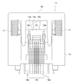
- FIG. 1 is a plan view of an IC socket according to an embodiment of the present invention.
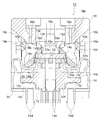
- FIG. 2 is a cross-sectional view taken along line AA of FIG. 1 according to the same embodiment.
- FIG. 2 is a right side view of FIG. 1 according to the same embodiment.
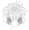
- It is a perspective view which shows the state which has the operation member of the IC socket which concerns on the embodiment in the highest position.
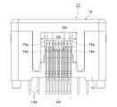
- It is the perspective view which fractured
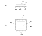
- FIG. 14 is an enlarged cross-sectional view illustrating a state where the IC package is slightly pressed downward by the pressing force of the latch from the state illustrated in FIG. 13 according to the same embodiment; It is a figure which shows IC package, (a) is a front view of IC package, (b) is a bottom view of IC package.
- 1 to 15 show an embodiment of the present invention.
- Reference numeral 11 in FIG. 1 denotes an IC socket as an “electrical component socket”.
- the IC socket 11 is arranged on a wiring board (not shown).
- the terminal 12b of the IC package 12 and its wiring board are electrically connected.
- the IC package 12 has a rectangular package body 12a in plan view, and a plurality of terminals 12b are formed on four sides on the lower surface of the peripheral edge of the package body 12a.
- the IC socket 11 is provided on the socket main body 13 having an accommodating surface portion 13 a for accommodating the IC socket 11, and contacts the terminals 12 b of the IC package 12.
- a contact pin 14 having an elastic piece 14a on which a contact portion 14b is formed, a latch 15 which is rotatably provided on the socket body 13 and holds the IC package 12 accommodated in the socket body 13 from above, and a socket
- the main body 13 has an operation member 16 provided to be movable up and down, and the latch 15 is rotated in the opening direction when the operation member 16 is lowered, and the latch 15 is rotated in the closing direction when the operation member 16 is raised. It is configured to let you.
- the socket body 13 is made of an insulating synthetic resin, and includes an upper member 13e and a lower member 13f, and is formed on the upper surface of the upper member 13e. Further, guide portions 13b for guiding the IC package 12 when it is accommodated are formed to protrude from the four corners around the accommodation surface portion 13a. Moreover, as shown in FIG. 2 etc., the lower part 13f of this socket main body 13 is formed with the attaching part 13c to which the several contact pin 14 is attached detachably from a horizontal direction so that it may protrude in four directions.
- the contact pin 14 is made of a conductive metal material and is formed in a so-called horseshoe shape. As shown in FIG. 2 and the like, the contact pin 14 is sandwiched from above and below the mounting portion 13c protruding from the socket body 13 in the lateral direction. It has the clamping part 14c attached to attachment or detachment. Thus, the contact pin 14 is detachably attached to the attachment portion 13c of the socket body 13 from the side.
- the contact pin 14 is extended substantially horizontally toward the inside after the elastic piece 14a is extended upward from the outer end of the mounting portion 13c, and the elastic piece 14a.
- the contact portion 14b is formed to extend upward from the front end portion.
- the contact portion 14b comes into contact with the terminal 12b of the IC package 12.
- a lead portion 14d extends downward from the pinching portion 14c to the contact pin 14, and the lead portion 14d is inserted into a wiring board (not shown) and soldered and fixed.
- a plurality of contact pins 14 are arranged adjacent to each other on the four sides of the peripheral edge of the socket body 13 in parallel at a predetermined pitch.
- the latch 15 is rotatably disposed on the socket body 13 at a position above the contact pins 14 provided at a plurality of four positions on each side of the IC package 12. Yes.
- the latch 15 is in the closed state, the upper part of the peripheral edge of the IC package 12 is pressed, and in the open state, the IC package 12 can be accommodated and taken out from the accommodating surface portion 13a.
- the latch 15 has a fan shape in which the width H1 on the front end side is narrow and the width H2 on the rear end side is wide in a plan view as shown in FIG.
- An opening 15f is formed in the central portion of the fan shape.
- a rotating shaft 15a is formed on both ends of the tip portion so as to protrude on both sides. As shown in FIG. 8, the rotating shafts 15a on both sides are sandwiched between the upper member 13e and the lower member 13f. And is held rotatably.
- the rotation shaft 15 a (fulcrum) is located below the accommodation surface portion 13 a of the socket body 13.
- the latch 15 is formed with a cam portion 15c as a “pushing portion” between a pair of rotating shafts 15a provided on both sides on the same axis.
- a cam portion 15c As shown in the left half of FIG.
- the elastic piece 14a By rotating the opening 15 in the opening direction, the elastic piece 14a is pressed by the cam portion 15c, the elastic piece 14a is elastically deformed downward, and the contact portion 14b is displaced downward.
- the cam portion is separated from the contact position with the terminal 12b of the IC package 12.
- the pressing of the elastic piece 14a of 15c is released and the elastic piece 14a is displaced upward by the elastic force of the elastic piece 14a, so that the contact portion 14b is raised to the contact position with the terminal 12b of the IC package 12.
- an escape inclined surface portion 15h is formed on the extension shaft of the rotation shaft 15a, so that the cross-sectional area is smaller than the rotation shaft 15a on both sides of the latch 15. .
- the latch 15 is formed with a pressing portion 15 d (operation point) that presses the upper surface of the IC package 12 and is opened when the operating member 16 is lowered.
- An operation target portion 15e (power point) is formed. When the opening operated portion 15e is pressed downward, the latch 15 is rotated in the opening direction.
- the opening operated portion 15e is formed on the outer edge side of the opening 15f at the substantially central portion on the rear end side where the width H2 of the latch 15 is wide.
- a pair of closing operated portions 15g (power points) projecting sideways are formed at both end portions on the rear end side where the width H2 of the latch 15 is wide (see FIG. 10 and the like).
- the pair of closed operated portions 15g are formed from the arrangement range width H3 of the plurality of contact pins 14 arranged side by side to a position protruding to the side, so that the pair of widths H4 of the latches 15 are The arrangement range is wider than the width H3 (see FIG. 9 and the like).
- the operation member 16 has a frame shape in plan view, and is disposed on the socket body 13 so as to be movable up and down.
- the operation member 16 is urged upward by springs 17 (see FIG. 3) provided at four locations, and rises to the highest level.
- springs 17 see FIG. 3
- the locking portion 16 a shown in FIG. 11 is locked to the locked portion 13 e formed in the socket body 13, so that upward movement is restricted. It has become.
- the operation member 16 has a central portion in the width direction of the latch 15 when the operation member 16 is moved downward from the highest position.
- An opening operation portion 16b that engages with the opening operation portion 15e and rotates the latch 15 in the opening direction is formed to extend obliquely downward on the inner side of the socket.
- a sliding surface 16c that presses and slides the opening operated portion 15e of the latch 15 is linearly formed as shown in FIG.
- the opening operating portion 16b is moved downward, the opening operating portion 16b is configured to be inserted into the opening 15f while pushing the opening operated portion 15g of the latch 15 downward.
- the tip of the opening operation portion 16b is inserted up to the extension line of the rotation shaft 15a of the opening portion 15f, and the opening operation portion 16b is vertically
- the front end surface 16d along the direction and the escape inclined surface portion 15h of the latch 15 are set so as to be substantially in contact with each other.
- the IC socket 11 having such a configuration is not provided with a conventional floating plate.
- the opening operated portion 15 e of the latch 15 opens the operating member 16.
- the latch 15 is pressed while sliding on the sliding surface 16c of the portion 16b, and the latch 15 is rotated in the opening direction around the rotation shaft 15a.
- the opening operation portion 16b of the operation member 16 is inserted to the far side of the opening 15f of the latch 15, and the pressing portion 15d of the latch 15 is retracted from the accommodation / removal range of the IC package 12. (See the left side in FIG. 2).
- the opening operating portion that presses the opening operated portion 15e at the center in the width direction of the latch 15 downward and rotates the latch 15 in the opening direction. Since the operation member 16 having 16b is provided, the space on both sides can be reduced as compared with the case where the space is pressed using the space on both sides of the latch 15, which contributes to the miniaturization of the IC socket 11.
- an opening 15f is formed in the central portion of the latch 15, and the opening operation portion 16b of the operation member 16 is opened on the rear side of the opening 15f of the latch 15 when moved downward. Since it is configured to be inserted into the opening 15f while pushing the operating portion 15e downward, the operating member 16 can be further moved to the inside of the socket body 13 and the outer shape of the IC socket 11 can be reduced. be able to.
- the opening operation portion 16b of the operation member 16 is linearly formed with a sliding surface 16c that presses and slides the opening operated portion 15e of the latch 15.
- the outer shape of the operation member 16 can be further reduced while securing the amount of rotation of the latch.
- the latch 15 is formed with a pair of rotating shafts 15a on both sides of the opening 15f, while the operating member 16 is in the lowest position, the tip of the opening operating portion 16b is rotated by the opening 15f. Since it is configured to be inserted up to the extended line of the moving shaft 15a, the operation member can be further moved to the inside of the socket body 13 and the outer shape of the IC socket 11 can be reduced.
- the tip of the opening operation portion 16b of the operation member 16 is inserted to the extension line of the rotating shaft 15a on the back side of the opening portion 15f of the latch 15, and the opening operation is performed.
- the front end surface 16d along the vertical direction of the portion 16b and the escape inclined surface portion 15h of the latch 15 are set so as to be substantially in contact with each other. 16 can be made as small as possible (see the left side of FIG. 2 and FIG. 5).
- the outermost position 15i when the latch 15 is opened to the maximum is a position that does not substantially protrude from the outermost position 14e of the contact pin 14. It does not protrude greatly. Therefore, the outer shape of the IC socket 11 can be made as small as possible, and the IC socket 11 can be downsized.
- the rotation center of the rotation shaft 15a of the latch 15 is located below the accommodation surface portion 13a of the socket body 13, the stroke of the latch 15 to the accommodation surface portion 13a can be increased. Even if the rotation amount of 15 is small, the IC package 12 can be pressed and released by the pressing portion 15d. Therefore, the vertical stroke of the operation member 16 can be shortened, and the vertical stroke of the IC socket 11 can be shortened, thereby reducing the size.
- the IC socket 11 can be downsized.
- the elastic piece 4a of the contact pin 14 is pressed and elastically deformed downward by the cam portion 15c of the latch 15, and the contact portion 14b of the contact pin 14 is moved downward.
- the position of the upper end of the contact portion 14b is located below the accommodation surface portion 13a (see the left side in FIG. 2).
- the IC package 12 is transported by an automatic machine, guided by the guide portion 13b of the socket body 13, and accommodated at a predetermined position of the accommodation surface portion 13a of the socket body 13 where the floating plate is not provided.
- the pair of closing operated portions 15 g of the latch 15 protrudes on both sides of the plurality of contact pins 14, and the pair of operating members 16 are closed.
- the operation portion 16c By disposing the operation portion 16c on both sides of the plurality of contact pins 14, it is not necessary to dispose a pair of closing operation portions 16c of the operation member 16 outside the contact pins 14 (see the right side of FIG. 2).
- the outer shape of the operation member 16 and, in turn, the socket body 13 can be reduced in size.
- the IC package 12 is slightly lowered against the urging force of the elastic piece 14a of the contact pin 14, and the terminal 12b of the IC package 12 and the contact portion 14b of the contact pin 14 are brought into contact with each other with a desired contact pressure. (See FIG. 14).
- the IC package 12 is electrically connected to the wiring board via the contact pins 14, whereby a burn-in test or the like is performed.
- the latch 15 hardly slides while pressing the upper surface of the IC package 12, it is difficult to make a mark on the upper surface of the IC package 12.
- the latch 15 is opened. At this time, the elastic piece 14a of the contact pin 14 is moved downward by the cam portion 15c of the latch 15. By forcibly displacing, adhesion between the contact portion 14b of the contact pin 14 and the terminal 12b of the IC package 12 can be reliably prevented.
- the elastic piece 14a of the contact pin 14 is elastically deformed by opening the latch 15 and the contact portion 14b is accommodated in the accommodation surface portion 13a.
- the IC package 12 can be accommodated at a predetermined position of the accommodation surface portion 13a.
- the elastic piece 14a is slightly lowered against the urging force of the elastic piece 14a, and the terminal 12b of the IC package 12 and the contact portion 14b of the contact pin 14 are brought into contact with each other with a desired contact pressure.
- the floating plate can be eliminated, the number of parts can be reduced, the tolerance of each part can be considered small, and the horizontal movement on the plane of the floating plate can be prevented. It can be placed at a predetermined position with high accuracy.
- the latch 15 has a so-called fan shape in which the front end side (inner side) width H1 is narrow and the rear end side (outer side) width H2 is wide. Since the operating portion 15e) is used for opening and the both end sides (closed operated portion 15g) are used for closing, it is not necessary to form an opening / closing structure in the space behind the latch 15, so that the IC The outer shape of the entire socket 11 can be made smaller.
- the contact pin 14 can also be detachably attached to the attachment portion 13c of the socket main body 13 from the lateral direction of the socket main body 13, so that the exchange work and the like can be performed very easily.
- the opening operated portion 15e of the latch 15 is disposed in the central portion in the width direction, the opening operated portion 15e in the central portion is pressed by the opening operating portion 16b of the operating member 16 so as to be opened. Therefore, the latch 15 can be opened and closed with a good balance only by pressing at one place.
- the present invention is applied to the IC socket 11 as the “socket for electrical parts”.
- the present invention is not limited to this and can be applied to other devices.
- the pushing portion of the latch is not limited to the cam portion, but may have other shapes.
Landscapes
- Engineering & Computer Science (AREA)
- Microelectronics & Electronic Packaging (AREA)
- Testing Of Individual Semiconductor Devices (AREA)
- Connecting Device With Holders (AREA)
- Coupling Device And Connection With Printed Circuit (AREA)
- Details Of Connecting Devices For Male And Female Coupling (AREA)
Abstract
Priority Applications (4)
| Application Number | Priority Date | Filing Date | Title |
|---|---|---|---|
| EP12764979.6A EP2573884B1 (fr) | 2011-03-31 | 2012-03-30 | Embase pour composant électrique |
| US13/634,455 US8801450B2 (en) | 2011-03-31 | 2012-03-30 | Socket having a rotatable latch with a pressing portion and a depressing portion |
| JP2012529997A JP6095982B2 (ja) | 2011-03-31 | 2012-03-30 | 電気部品用ソケット |
| CN201280001675.7A CN102986093B (zh) | 2011-03-31 | 2012-03-30 | 电气零件用插座 |
Applications Claiming Priority (4)
| Application Number | Priority Date | Filing Date | Title |
|---|---|---|---|
| JP2011-077763 | 2011-03-31 | ||
| JP2011077763 | 2011-03-31 | ||
| JP2011288137 | 2011-12-28 | ||
| JP2011-288137 | 2011-12-28 |
Publications (1)
| Publication Number | Publication Date |
|---|---|
| WO2012133740A1 true WO2012133740A1 (fr) | 2012-10-04 |
Family
ID=46931438
Family Applications (1)
| Application Number | Title | Priority Date | Filing Date |
|---|---|---|---|
| PCT/JP2012/058526 Ceased WO2012133740A1 (fr) | 2011-03-31 | 2012-03-30 | Embase pour composant électrique |
Country Status (5)
| Country | Link |
|---|---|
| US (1) | US8801450B2 (fr) |
| EP (1) | EP2573884B1 (fr) |
| JP (1) | JP6095982B2 (fr) |
| CN (1) | CN102986093B (fr) |
| WO (1) | WO2012133740A1 (fr) |
Cited By (3)
| Publication number | Priority date | Publication date | Assignee | Title |
|---|---|---|---|---|
| US8801450B2 (en) | 2011-03-31 | 2014-08-12 | Enplas Corporation | Socket having a rotatable latch with a pressing portion and a depressing portion |
| WO2021149417A1 (fr) * | 2020-01-21 | 2021-07-29 | 株式会社エンプラス | Douille |
| US20230184826A1 (en) * | 2021-11-03 | 2023-06-15 | Johnstech International Corporation | Housing with vertical backstop |
Families Citing this family (2)
| Publication number | Priority date | Publication date | Assignee | Title |
|---|---|---|---|---|
| JP6445340B2 (ja) * | 2015-02-06 | 2018-12-26 | 株式会社エンプラス | 電気部品用ソケット |
| US11569601B2 (en) * | 2021-03-11 | 2023-01-31 | Enplas Corporation | Socket and inspection socket |
Citations (7)
| Publication number | Priority date | Publication date | Assignee | Title |
|---|---|---|---|---|
| JPH01104684U (fr) * | 1987-12-31 | 1989-07-14 | ||
| JPH0636843A (ja) * | 1992-07-16 | 1994-02-10 | Texas Instr Japan Ltd | ソケット |
| JPH0660951A (ja) * | 1992-07-06 | 1994-03-04 | Wells Electronics Inc | ソケット |
| JPH07282932A (ja) * | 1994-04-07 | 1995-10-27 | Enplas Corp | Icソケット |
| JP2002343520A (ja) * | 2001-05-10 | 2002-11-29 | Wells Cti Kk | Icソケット |
| JP2002343522A (ja) * | 2001-05-10 | 2002-11-29 | Wells Cti Kk | Icソケット |
| JP2007059117A (ja) | 2005-08-23 | 2007-03-08 | Enplas Corp | 電気部品用ソケット |
Family Cites Families (15)
| Publication number | Priority date | Publication date | Assignee | Title |
|---|---|---|---|---|
| JPH07110941B2 (ja) | 1987-10-19 | 1995-11-29 | 化成オプトニクス株式会社 | 発光組成物 |
| JP2742502B2 (ja) * | 1993-10-18 | 1998-04-22 | 山一電機株式会社 | ダスト排出手段を備えたicソケット |
| JPH08227769A (ja) * | 1995-02-21 | 1996-09-03 | Toshiba Corp | Icソケット |
| JP2816132B2 (ja) * | 1996-03-26 | 1998-10-27 | 山一電機株式会社 | Icソケットにおけるic押え機構 |
| JPH09306624A (ja) * | 1996-05-17 | 1997-11-28 | Texas Instr Japan Ltd | ソケット |
| JPH10125427A (ja) * | 1996-10-21 | 1998-05-15 | Enplas Corp | Icソケット |
| US6283780B1 (en) * | 1998-04-01 | 2001-09-04 | Molex Incorporated | Test socket lattice |
| JP4721582B2 (ja) * | 2001-09-14 | 2011-07-13 | 株式会社センサータ・テクノロジーズジャパン | ソケット |
| JP2003168532A (ja) * | 2001-11-29 | 2003-06-13 | Texas Instr Japan Ltd | 半導体装置用ソケットおよび半導体装置のソケットへの取付け方法 |
| JP4271406B2 (ja) * | 2002-04-09 | 2009-06-03 | 株式会社エンプラス | 電気部品用ソケット |
| JP4347027B2 (ja) * | 2003-11-28 | 2009-10-21 | 株式会社エンプラス | 電気部品用ソケット |
| CN102986093B (zh) | 2011-03-31 | 2016-03-23 | 恩普乐股份有限公司 | 电气零件用插座 |
| JP5836113B2 (ja) * | 2011-12-28 | 2015-12-24 | 株式会社エンプラス | 電気部品用ソケット |
| US8888503B2 (en) * | 2011-12-28 | 2014-11-18 | Enplas Corporation | Socket for electric parts |
| JP5836112B2 (ja) * | 2011-12-28 | 2015-12-24 | 株式会社エンプラス | 電気部品用ソケット |
-
2012
- 2012-03-30 CN CN201280001675.7A patent/CN102986093B/zh not_active Expired - Fee Related
- 2012-03-30 WO PCT/JP2012/058526 patent/WO2012133740A1/fr not_active Ceased
- 2012-03-30 US US13/634,455 patent/US8801450B2/en not_active Expired - Fee Related
- 2012-03-30 EP EP12764979.6A patent/EP2573884B1/fr not_active Not-in-force
- 2012-03-30 JP JP2012529997A patent/JP6095982B2/ja not_active Expired - Fee Related
Patent Citations (7)
| Publication number | Priority date | Publication date | Assignee | Title |
|---|---|---|---|---|
| JPH01104684U (fr) * | 1987-12-31 | 1989-07-14 | ||
| JPH0660951A (ja) * | 1992-07-06 | 1994-03-04 | Wells Electronics Inc | ソケット |
| JPH0636843A (ja) * | 1992-07-16 | 1994-02-10 | Texas Instr Japan Ltd | ソケット |
| JPH07282932A (ja) * | 1994-04-07 | 1995-10-27 | Enplas Corp | Icソケット |
| JP2002343520A (ja) * | 2001-05-10 | 2002-11-29 | Wells Cti Kk | Icソケット |
| JP2002343522A (ja) * | 2001-05-10 | 2002-11-29 | Wells Cti Kk | Icソケット |
| JP2007059117A (ja) | 2005-08-23 | 2007-03-08 | Enplas Corp | 電気部品用ソケット |
Non-Patent Citations (1)
| Title |
|---|
| See also references of EP2573884A4 |
Cited By (6)
| Publication number | Priority date | Publication date | Assignee | Title |
|---|---|---|---|---|
| US8801450B2 (en) | 2011-03-31 | 2014-08-12 | Enplas Corporation | Socket having a rotatable latch with a pressing portion and a depressing portion |
| WO2021149417A1 (fr) * | 2020-01-21 | 2021-07-29 | 株式会社エンプラス | Douille |
| JP2021114447A (ja) * | 2020-01-21 | 2021-08-05 | 株式会社エンプラス | ソケット |
| JP7455593B2 (ja) | 2020-01-21 | 2024-03-26 | 株式会社エンプラス | ソケット |
| US20230184826A1 (en) * | 2021-11-03 | 2023-06-15 | Johnstech International Corporation | Housing with vertical backstop |
| US12487279B2 (en) * | 2021-11-03 | 2025-12-02 | Johnstech International Corporation | Housing with vertical backstop |
Also Published As
| Publication number | Publication date |
|---|---|
| CN102986093A (zh) | 2013-03-20 |
| CN102986093B (zh) | 2016-03-23 |
| EP2573884B1 (fr) | 2017-05-24 |
| JPWO2012133740A1 (ja) | 2014-07-28 |
| US20130280938A1 (en) | 2013-10-24 |
| EP2573884A4 (fr) | 2015-04-15 |
| EP2573884A1 (fr) | 2013-03-27 |
| JP6095982B2 (ja) | 2017-03-15 |
| US8801450B2 (en) | 2014-08-12 |
Similar Documents
| Publication | Publication Date | Title |
|---|---|---|
| JP4963085B2 (ja) | Bga用ソケット | |
| US20070270014A1 (en) | Socket for electrical parts | |
| JP4322635B2 (ja) | 電気部品用ソケット | |
| JP6095982B2 (ja) | 電気部品用ソケット | |
| JP5836112B2 (ja) | 電気部品用ソケット | |
| JP4464250B2 (ja) | 電気部品用ソケット | |
| JP5836113B2 (ja) | 電気部品用ソケット | |
| JP4347027B2 (ja) | 電気部品用ソケット | |
| JP4676841B2 (ja) | 電気部品用ソケット | |
| JP2003168534A (ja) | 電気部品用ソケット | |
| JP2001326043A (ja) | 電気部品用ソケット | |
| US7407401B2 (en) | Socket for electrical parts | |
| JP6660683B2 (ja) | 電気部品用ソケット | |
| JP2004228042A (ja) | 電気部品用ソケット | |
| EP2611269B1 (fr) | Douille pour des parties électriques | |
| JP2019021399A (ja) | 電気部品用ソケット | |
| CN201498851U (zh) | 电连接器 | |
| JP4767745B2 (ja) | 電気部品用ソケット | |
| JP3776338B2 (ja) | 電気部品用ソケット | |
| JP4326632B2 (ja) | 電気部品用ソケット | |
| JP2004047163A (ja) | 電気部品用ソケット | |
| JP2006127935A (ja) | 電気部品用ソケット | |
| JP5202275B2 (ja) | 電気部品用ソケット | |
| JP2004014133A (ja) | 電気部品用ソケット | |
| JP2007115500A (ja) | 電気部品用ソケット |
Legal Events
| Date | Code | Title | Description |
|---|---|---|---|
| WWE | Wipo information: entry into national phase |
Ref document number: 201280001675.7 Country of ref document: CN |
|
| ENP | Entry into the national phase |
Ref document number: 2012529997 Country of ref document: JP Kind code of ref document: A |
|
| WWE | Wipo information: entry into national phase |
Ref document number: 13634455 Country of ref document: US |
|
| 121 | Ep: the epo has been informed by wipo that ep was designated in this application |
Ref document number: 12764979 Country of ref document: EP Kind code of ref document: A1 |
|
| REEP | Request for entry into the european phase |
Ref document number: 2012764979 Country of ref document: EP |
|
| WWE | Wipo information: entry into national phase |
Ref document number: 2012764979 Country of ref document: EP |
|
| NENP | Non-entry into the national phase |
Ref country code: DE |