WO2012134175A2 - Conductive substrate and touchscreen having same - Google Patents
Conductive substrate and touchscreen having same Download PDFInfo
- Publication number
- WO2012134175A2 WO2012134175A2 PCT/KR2012/002285 KR2012002285W WO2012134175A2 WO 2012134175 A2 WO2012134175 A2 WO 2012134175A2 KR 2012002285 W KR2012002285 W KR 2012002285W WO 2012134175 A2 WO2012134175 A2 WO 2012134175A2
- Authority
- WO
- WIPO (PCT)
- Prior art keywords
- electrically conductive
- conductive pattern
- substrate
- pattern
- vertices
- Prior art date
- Legal status (The legal status is an assumption and is not a legal conclusion. Google has not performed a legal analysis and makes no representation as to the accuracy of the status listed.)
- Ceased
Links
Classifications
-
- G—PHYSICS
- G06—COMPUTING OR CALCULATING; COUNTING
- G06F—ELECTRIC DIGITAL DATA PROCESSING
- G06F3/00—Input arrangements for transferring data to be processed into a form capable of being handled by the computer; Output arrangements for transferring data from processing unit to output unit, e.g. interface arrangements
- G06F3/01—Input arrangements or combined input and output arrangements for interaction between user and computer
- G06F3/03—Arrangements for converting the position or the displacement of a member into a coded form
- G06F3/041—Digitisers, e.g. for touch screens or touch pads, characterised by the transducing means
- G06F3/044—Digitisers, e.g. for touch screens or touch pads, characterised by the transducing means by capacitive means
- G06F3/0446—Digitisers, e.g. for touch screens or touch pads, characterised by the transducing means by capacitive means using a grid-like structure of electrodes in at least two directions, e.g. using row and column electrodes
-
- G—PHYSICS
- G02—OPTICS
- G02F—OPTICAL DEVICES OR ARRANGEMENTS FOR THE CONTROL OF LIGHT BY MODIFICATION OF THE OPTICAL PROPERTIES OF THE MEDIA OF THE ELEMENTS INVOLVED THEREIN; NON-LINEAR OPTICS; FREQUENCY-CHANGING OF LIGHT; OPTICAL LOGIC ELEMENTS; OPTICAL ANALOGUE/DIGITAL CONVERTERS
- G02F1/00—Devices or arrangements for the control of the intensity, colour, phase, polarisation or direction of light arriving from an independent light source, e.g. switching, gating or modulating; Non-linear optics
- G02F1/01—Devices or arrangements for the control of the intensity, colour, phase, polarisation or direction of light arriving from an independent light source, e.g. switching, gating or modulating; Non-linear optics for the control of the intensity, phase, polarisation or colour
- G02F1/13—Devices or arrangements for the control of the intensity, colour, phase, polarisation or direction of light arriving from an independent light source, e.g. switching, gating or modulating; Non-linear optics for the control of the intensity, phase, polarisation or colour based on liquid crystals, e.g. single liquid crystal display cells
- G02F1/133—Constructional arrangements; Operation of liquid crystal cells; Circuit arrangements
- G02F1/1333—Constructional arrangements; Manufacturing methods
- G02F1/13338—Input devices, e.g. touch panels
-
- G—PHYSICS
- G06—COMPUTING OR CALCULATING; COUNTING
- G06F—ELECTRIC DIGITAL DATA PROCESSING
- G06F3/00—Input arrangements for transferring data to be processed into a form capable of being handled by the computer; Output arrangements for transferring data from processing unit to output unit, e.g. interface arrangements
- G06F3/01—Input arrangements or combined input and output arrangements for interaction between user and computer
- G06F3/03—Arrangements for converting the position or the displacement of a member into a coded form
- G06F3/041—Digitisers, e.g. for touch screens or touch pads, characterised by the transducing means
-
- G—PHYSICS
- G06—COMPUTING OR CALCULATING; COUNTING
- G06F—ELECTRIC DIGITAL DATA PROCESSING
- G06F3/00—Input arrangements for transferring data to be processed into a form capable of being handled by the computer; Output arrangements for transferring data from processing unit to output unit, e.g. interface arrangements
- G06F3/01—Input arrangements or combined input and output arrangements for interaction between user and computer
- G06F3/03—Arrangements for converting the position or the displacement of a member into a coded form
- G06F3/041—Digitisers, e.g. for touch screens or touch pads, characterised by the transducing means
- G06F3/044—Digitisers, e.g. for touch screens or touch pads, characterised by the transducing means by capacitive means
- G06F3/0443—Digitisers, e.g. for touch screens or touch pads, characterised by the transducing means by capacitive means using a single layer of sensing electrodes
-
- H—ELECTRICITY
- H05—ELECTRIC TECHNIQUES NOT OTHERWISE PROVIDED FOR
- H05K—PRINTED CIRCUITS; CASINGS OR CONSTRUCTIONAL DETAILS OF ELECTRIC APPARATUS; MANUFACTURE OF ASSEMBLAGES OF ELECTRICAL COMPONENTS
- H05K1/00—Printed circuits
- H05K1/02—Details
- H05K1/0274—Optical details, e.g. printed circuits comprising integral optical means
-
- B—PERFORMING OPERATIONS; TRANSPORTING
- B32—LAYERED PRODUCTS
- B32B—LAYERED PRODUCTS, i.e. PRODUCTS BUILT-UP OF STRATA OF FLAT OR NON-FLAT, e.g. CELLULAR OR HONEYCOMB, FORM
- B32B2457/00—Electrical equipment
- B32B2457/20—Displays, e.g. liquid crystal displays, plasma displays
- B32B2457/208—Touch screens
-
- G—PHYSICS
- G06—COMPUTING OR CALCULATING; COUNTING
- G06F—ELECTRIC DIGITAL DATA PROCESSING
- G06F2203/00—Indexing scheme relating to G06F3/00 - G06F3/048
- G06F2203/041—Indexing scheme relating to G06F3/041 - G06F3/045
- G06F2203/04103—Manufacturing, i.e. details related to manufacturing processes specially suited for touch sensitive devices
-
- G—PHYSICS
- G06—COMPUTING OR CALCULATING; COUNTING
- G06F—ELECTRIC DIGITAL DATA PROCESSING
- G06F2203/00—Indexing scheme relating to G06F3/00 - G06F3/048
- G06F2203/041—Indexing scheme relating to G06F3/041 - G06F3/045
- G06F2203/04112—Electrode mesh in capacitive digitiser: electrode for touch sensing is formed of a mesh of very fine, normally metallic, interconnected lines that are almost invisible to see. This provides a quite large but transparent electrode surface, without need for ITO or similar transparent conductive material
Definitions
- the present invention relates to a conductive substrate and a touch screen including the same.
- a display device is a term used throughout a monitor for a TV or a computer, and includes a display element for forming an image and a case for supporting the display element.
- the display device includes a plasma display panel (PDP), a liquid crystal display (LCD), an electrophoretic display, an electrophoretic display, and a cathode ray tube (CRT). ), An OLED display, and the like.
- PDP plasma display panel
- LCD liquid crystal display
- electrophoretic display an electrophoretic display
- CRT cathode ray tube
- OLED display an OLED display, and the like.
- the display device may be equipped with an RGB pixel pattern and an additional optical filter for image realization.
- the touch screen having the above function is as follows according to a signal and a detection method; Can be classified as
- a resistive type that detects a position pressed by pressure in a state in which a DC voltage is applied through a change in current or a voltage value, and a capacitance coupling in a state where an AC voltage is applied.
- the most common resistive and capacitive touch screens use a transparent conductive film such as ⁇ film to recognize whether the touch is caused by electrical contact or change in capacitance.
- the transparent conductive film has a high or low term of 150 ohm / square or more, the sensitivity of the transparent conductive film is largely reduced, and thus, the touch screen fabrication process uses the patterning process of ⁇ and the electrode patterning process of the metal trace part such as photolithography.
- the cost of ITO film increases rapidly as the size of the screen increases, making it difficult to increase the manufacturing cost and apply the large size.
- an attempt has been made to realize an increase in size by using a metal pattern with high conductivity. This metal pattern is advantageous for large area due to the high conductivity of the metal, and has advantages in yield and price due to the reduction of the number of processes in terms of simultaneously forming the trace electrode and the screen part. .
- the moiré phenomenon is a phenomenon in which another interference pattern is formed by the interference between the display pixels and the pattern when a regular pattern exists on the pixel pattern or the electrode pattern of the display. As well as inhibiting pixel distortion, It causes a problem.
- the electrically conductive pattern includes an edge structure of closed figures connected in series , and the electrically conductive pattern has no closed figure of the same type in an arbitrary unit area (lcm X lcm) and has the number of vertices of the closed figures. Provides a conductive substrate that is different from the number of vertices of the same number of squares as the closed figures.
- a substrate and an electrically conductive pattern provided on at least one side of the substrate.
- the electrically conductive pattern includes a border structure of continuously connected closed figures, and the electrically conductive pattern does not have the same closed figure in an arbitrary unit area (lcm X lcm), and the number of vertices of the closed figures.
- the electrically conductive pattern includes an edge structure of continuously connected closed figures, and the electrically conductive pattern does not have a closed figure of the same type within an arbitrary unit area (lcm X lcm), and the closed figures are It provides a conductive substrate having a value of Equation 1 is 50 or more.
- a conductive substrate comprising a substrate, and an electrically conductive pattern provided on at least one side of the substrate,
- the image When the straight light emitted from the light source is irradiated on one surface of the conductive substrate to obtain an image of a transmission diffraction pattern, the image provides a conductive organ having a value of Equation 2 below.
- the angular region means a region in which 0 to 360 degrees are divided by 10 degrees from the center of the image of the transmission diffraction pattern.
- another embodiment of the present invention provides a touch screen including an additional transparent substrate on the electrically conductive pattern of the conductive substrate.
- another exemplary embodiment of the present invention provides a display including the touch screen and display modules.
- the conductive substrate and the touch screen including the same according to the present invention not only have excellent conductivity without covering the field of view, but also can reduce reflection diffraction caused by a point light source, and furthermore, display quality due to moire phenomenon. It can prevent the degradation.
- the electrically conductive pattern according to the present invention may be formed by various methods such as indirect printing, photolithography, photography, hard mask, sputtering, etc. after the desired pattern is predetermined. The process is easy and inexpensive.
- 1 is a view showing the value (average of the distance between the vertices and the standard deviation I vertex of the distance between the vertices) according to the irregularity of the electrically conductive pattern according to an embodiment of the present invention.
- FIG. 2 is a view showing the distance between the vertices of the electrically conductive pattern according to an embodiment of the present invention.
- FIG 3 is a view showing the number distribution according to the angle of the components of each side constituting the electrically conductive pattern according to an embodiment of the present invention.
- FIG. 4 is a diagram showing the configuration of an apparatus for measuring the total reflectance of the conductive substrate according to one embodiment of the present invention.
- FIG. 5 is a diagram showing a total reflectance graph of the conductive substrate according to one embodiment of the present invention.
- FIG. 6 is a view showing a reflective diffraction apparatus for evaluating optical characteristics of a conductive substrate according to one embodiment of the present invention.
- FIG. 7 is a diagram illustrating a reflective diffraction image of a conventional conductive substrate.
- An object of the present invention is to propose a method and criteria for evaluating reflective diffraction for use in an actual display, as well as a method for minimizing a reflective diffraction caused by a point light source when using a regularly ordered pattern. Furthermore, it is an object of the present invention to provide a pattern design method for fundamentally solving the moire phenomenon mentioned at the beginning, a conductor including the same, and a touch screen including the same.
- an electrically conductive pattern formed in a regular pattern of one type such as a grid method or a linear method, may be applied to a display having a regular internal structure, such as a pixel structure, or an optical having a regular pattern structure.
- a display including a film or an electrode structure there is a problem that moiré phenomenon occurs due to relative interference between patterns due to light sources adjacent to these pattern structures, and when such moiré phenomenon occurs, visual recognition (visibility) Will fall.
- the conductive substrate according to the present invention includes a substrate and an electrically conductive pattern provided on at least one side of the substrate.
- An exemplary embodiment of the present invention includes a substrate, and an electrically conductive conductive pattern provided on at least one surface of the substrate, wherein the electrically conductive pattern includes an edge structure of closed chains continuously connected, and the electrically conductive pattern is There is no closed figure of the same shape in any unit area (lcm X lcm), and the number of vertices of the closed figures is different from the number of vertices of the same number of squares as the closed figures. do.
- the number of vertices of the closed figures is different from the number of vertices of the same number of squares as the closed figures. More specifically, the number of vertices of the closed figures is the same number of squares as the closed figures. Compared to the number of vertices of the types may be more, 1.9 to 2.1 times more, but is not limited to this.
- the closed figures are continuously connected to each other.
- the closed figures may be in the form of sharing at least one side.
- the substrate and includes an electrically conductive pattern provided on at least one surface on the substrate, the electrically conductive pattern comprises a border structure of closed figures connected in series, the electrically conductive The pattern does not have a closed figure of the same shape in any unit area (lcm X lcm), and the number of vertices of the closed figure is formed by connecting the shortest distance between the centers of gravity of each of the closed figures.
- a conductive substrate is provided that is different from the number of vertices of one polygon.
- the number of vertices of the closed figures is different from the number of vertices of the polygon formed by connecting the shortest distance between the centers of gravity of each of the closed figures. More specifically, the number of vertices of the closed figures may be greater than the number of vertices ⁇ 1 of polygons formed by connecting the shortest distances between the centers of gravity of each of the closed figures, and may be 1.9 to 2.1 times more.
- the present invention is not limited thereto.
- the substrate and includes an electrically conductive pattern provided on at least one surface on the substrate, the electrically conductive pattern comprises a border structure of closed figures connected in series, the electrically conductive
- the pattern provides a conductive substrate in which no closed figure of the same shape exists in any unit area (lcm ⁇ lcm), and the closed figure have a value of Equation 1 below.
- another exemplary embodiment of the present invention is a conductive substrate including a substrate and an electrically conductive pattern provided on at least one surface of the substrate, wherein the one side of the conductive substrate is irradiated with straight light emitted from a light source to transmit a diffraction pattern When obtaining the image of the, the image is removed to the conductive substrate that the value of Equation 2 Ball.
- the angular region means a region in which 0 to 360 degrees are divided by 10 degrees from the center of the image of the transmission diffraction pattern.
- the image of the transmission diffraction pattern when the image of the transmission diffraction pattern is obtained, the image may have a value of Equation 2 below 21, 15 or less, and 10 or less.
- the electrically conductive pattern includes a border structure of closed figures continuously connected, and the border structure of the closed figures may be variously modified such as a straight line, a curve, a zigzag, a combination thereof, and the like.
- the electrically conductive patterns may not have the same closed figure in the unit area.
- the electrically conductive pattern includes an edge structure of closed figures connected in series, and an angle at 0 to 180 degrees that forms lines constituting the edges of the closed figures with respect to any straight line.
- the value of Equation 3 may be less than 21, may be less than 15, may be less than 10.
- the values of Equations 1 to 3 may be calculated within a unit area of the electrically conductive pattern.
- the unit area may be an area in which an electrically conductive pattern is formed, for example, 3.5 cm X 3.5 cm, but is not limited thereto.
- the numerical values of the above Equations 1 to 3 may be supported by tables and drawings of the embodiments and the like.
- the vertex is defined as meaning that the lines constituting the edges of the closed figures of the electrically conductive pattern cross each other.
- the present invention may further include a transparent substrate on the surface of the electrically conductive pattern is visible.
- the additional transparent substrate may include reinforcing glass, transparent plastic, and the like, but is not limited thereto.
- the conductive substrate including the electrically conductive pattern may form an electrically conductive layer by a deposition method such as a sputtering method, a CVlX chemical vapor deposition method, a thermal evaporation method, an e-beam deposition method, or the like. And, by patterning it it is possible to form an electrically conductive pattern.
- a deposition method such as a sputtering method, a CVlX chemical vapor deposition method, a thermal evaporation method, an e-beam deposition method, or the like. And, by patterning it it is possible to form an electrically conductive pattern.
- the electrically conductive pattern includes a border structure of the closed figures connected in series, the number of vertices of the closed figure is different from the number of vertices of the same number of squares as the closed figures. .
- the electrically conductive pattern includes a border structure of the closed figures connected in series, the number of vertices of the closed figures, formed by connecting the shortest distance between the center of gravity of each of the closed figures And different numbers of vertices of the polygon.
- the electrically conductive pattern is a closing diagram connected in series It includes a border structure of the type, the closed figure is characterized in that the value of the equation (1) is 50 or more.
- an electrical conductive pattern according to the present invention after arranging arbitrary points in a regularly arranged unit unit cell, each point is connected to a point closest to a distance from other points, and thus the shape of a border structure of closed figures. Can be.
- an electrical conductive pattern according to the present invention may be formed when an irregularity is introduced in a method of arranging arbitrary points in the regularly arranged unit unit cells. For example, when the irregularity is set to 0, if the unit unit cell is square, an electrically conductive pattern has a square mesh structure. If the unit unit cell is a regular hexagon, an electrically conductive pattern has a honeycomb structure. do. That is, in the electrically conductive pattern according to the present invention, the irregularity means a pattern other than zero.
- the electrically conductive pattern of the irregular pattern form according to the present invention, it is possible to suppress the tendency of the line forming the pattern, and to obtain a uniform transmittance from the display and to maintain the same line density for the unit area It is possible to ensure a uniform conductivity.
- the material of the electrically conductive pattern is not particularly limited, but is preferably metal.
- the material of the electrically conductive pattern is preferably a material having excellent conductivity and easy etching.
- the total reflectance can be lowered, the visibility of the electrically conductive pattern can be lowered, and the contrast characteristics can be maintained or improved.
- the material of the electrically conductive pattern are a single film or a multilayer film including gold, silver, aluminum, copper, neodymium, molybdenum, nickel or alloys thereof.
- the thickness of the electrically conductive pattern is not particularly limited, but is preferably 0.01 to 10 m in view of the conductivity of the electrically conductive pattern and the economics of the forming process.
- the electrically conductive pattern may be formed using an etching resist pattern.
- the etching resist pattern is printed, photolithography, photography, mask It can be formed using a method or laser transfer, for example, thermal transfer imaging, and printing or photolithography is more preferred.
- the electrically conductive pattern may be etched using the etching resist pattern, and the etching resist pattern may be removed.
- the electrically conductive pattern may have a line width of 10 or less, 7 or less, 5 or less, 5 or less, 4 or less, or 0.1 or more. More specifically, the electrically conductive pattern may be a line width of 0.1 ⁇ 1im, 1-2im, 2-, 4 ⁇ 5j3 ⁇ 4m, 5 ⁇ 7 /, but is not limited thereto.
- the line width of the electrically conductive pattern may be 10 or less and the thickness may be 10 // m or less, the line width of the electrically conductive pattern may be 7 // m or less and the thickness may be 1 or less, and the line width of the conductive pattern is 5 / ⁇ or less and the thickness may be 0.5 mi or less.
- the electrically conductive pattern may be at least 6,000 vertices, at least 7,000, at least 15,000, and at most 245,000 in the unit area (3.5 cm X 3.5 cm). However, this can be adjusted by those skilled in the art according to the desired transmittance and conductivity.
- the line width of the electrically conductive pattern may be 10 or less, and the number of vertices of the closed figures may be 6,000 to 245,000 in an area of 3.5 cm x 3.5 cm.
- the line width of the electrically conductive pattern is 7 ⁇ or less, the electrically conductive pattern may be the number of vertices of the closed figures in the area of 3.5cm ⁇ 3.5cm 7,000 ⁇ 62,000.
- the line width of the electrically conductive pattern is 5 / / m or less, the electrically conductive pattern may be 15,000 ⁇ 62,000 the number of vertices of the closed figures in an area of 3.5cm x 3.5cm.
- the opening ratio of the electrically conductive pattern that is, the area ratio not covered by the pattern may be 70% or more, 85% or more, or 95% or more.
- the opening ratio of the electrically conductive pattern may be 90 to 99.9%, but is not limited thereto.
- the electrically conductive pattern used in the present invention has a resistivity of 1 X 10 6 um 'cm to 30
- a material of ⁇ 10 6 um ⁇ is suitable, and more preferably 7 X 10 6 um : (: 111 or less).
- the sheet resistance of the conductive substrate may be 1 to 300 ohms / square. Mine is advantageous for the operation of the touch screen.
- the side of the electrically conductive pattern may have a forward taper angle, but the conductive pattern located on the opposite side of the substrate side of the conductive pattern may have an inverse taper angle.
- the touch screen according to the present invention may further include an additional conductive substrate in addition to the conductive substrate including the above-described substrate and the electrically conductive pattern.
- an electrically conductive pattern may be provided on both surfaces of the substrate.
- the touch screen according to the present invention may further include an electrode part or a pad part in addition to the effective screen part in which the electrically conductive pattern is formed on the conductive substrate, wherein the effective screen part and the electrode part I pad part are made of the same conductor. It may have the same thickness and may be seamless.
- the touch screen according to the present invention may include a protective film, a polarizing film, an antireflection film, an anti-glare film, an anti-fingerprint film, a low reflection film, and the like on one surface of each substrate.
- the aperture ratio of the touch screen according to the present invention that is, the area ratio not covered by the pattern may be 70% or more, 85% or more, or 95% or more.
- the aperture ratio of the touch screen may be 90 to 99.9%, but is not limited thereto.
- the conductive substrate according to the present invention may further include a darkening layer provided on at least one surface of the electrically conductive pattern and provided in a region corresponding to the electrically conductive pattern.
- the reflective diffraction intensity of the reflective diffraction image obtained by irradiating light from a point light source on one surface where the darkening layer is visible except that the electrically conductive pattern is made of A1 and does not include a darkening layer. And it may be reduced by more than 60% compared to the conductive substrate having the same configuration.
- the reflective diffraction intensity, the electrically conductive pattern is made of A1 and does not include a darkening layer
- the conductive substrate having the same configuration except that it may be reduced by more than 60% may be reduced by more than 70%, may be reduced by more than 80%. For example, it may be 60 to 70% reduced, 70 to 80% reduced, and 80 to 85% reduced.
- the total reflectance may be reduced by more than 20% compared to a conductive substrate having the same configuration except that the electrically conductive pattern is made of A1 and does not include a darkening layer, and may be reduced by more than 25%. It may be reduced by more than 30%. For example, it may be reduced by 25 to 50%.
- the darkening layer may be provided on the top and bottom surfaces of the electrically conductive pattern, and may be provided on at least a portion of the side surfaces as well as the top and bottom surfaces of the electrically conductive pattern, and the top, bottom and side surfaces of the electrically conductive pattern. It may be provided in the whole.
- the darkening layer may be provided on the entire surface of the electrically conductive pattern to reduce visibility due to the high reflectivity of the electrically conductive pattern.
- the darkening layer since the darkening layer has an extinction interference and its own absorbance under a certain thickness condition when combined with a layer having a high reflectivity such as a conductive layer, the darkening layer reflects the conductive pattern through the light and the darkening layer reflected by the darkening layer. By adjusting the amount of reflected light similarly to each other and inducing mutual interference between two lights under a certain thickness condition, the reflectivity by the conductive pattern is reduced.
- the color range of the pattern region consisting of the darkening layer and the electrically conductive pattern, measured from the view of the darkening layer of the conductive substrate according to the present invention L value is 20 or less, A value is based on the CIE LAB color coordinates -10-10, B value can be -70 ⁇ 70, L value is 10 or less, A value is -5 ⁇ 5, B value can be 0 ⁇ 35, L value is 5 or less , A The value can be -2 to 2 and the B value can be 0 to 15.
- the total reflectance of the pattern region consisting of the darkened layer and the electrically conductive pattern measured from the perspective of the darkened layer of the conductive substrate according to the present invention, may be 17% or less, based on external light 550nm, and 10% It may be less than or equal to 5%.
- total reflectance means total reflectance in consideration of both a diffuse reflectance and a specular reflectance.
- the total reflectance is a value observed by measuring only the reflectivity of the surface to be measured after making the reflectance ⁇ by using a black paste or a tape on the opposite side of the surface on which the reflectance is to be measured.
- the incoming light source introduced a diffuse light source most similar to the ambient light condition.
- the measurement position for measuring the reflectance was based on a position inclined about 7 degrees from the vertical line of the integrating sphere semicircle.
- 4 shows a configuration of a device for measuring the total reflectance
- FIG. 5 shows a total reflectance graph of the conductive substrate according to one embodiment of the present invention.
- the darkening layer or simultaneously with the electrically conductive pattern.
- the layers for forming each pattern are formed separately.
- a separate pattern layer forms a stacked structure, and at least a portion of the light absorbing material is formed in a structure or a single conductive layer in which the light absorbing material is embedded or dispersed in the electrically conductive pattern.
- Surface treatment is different from the structure in which part of the surface side is physically or chemically modified.
- the darkening layer is an adhesive layer or It is provided directly on the substrate or directly on the electrically conductive pattern without interposing the adhesive layer.
- the adhesive layer or adhesive layer may affect durability or optical properties.
- the laminate included in the touch screen according to the present invention has a completely different manufacturing method compared with the case of using an adhesive layer or an adhesive layer.
- the interface characteristic of a base material or an electrically conductive pattern, and a darkening layer is excellent.
- the darkening layer may be formed of a single layer or may be formed of two or more layers.
- the mall darkening layer is close to the color of achromatic color system.
- the achromatic color means a color that appears when light incident on the surface of an object is not selectively absorbed and is evenly reflected and absorbed for the wavelength of each component.
- the darkening pattern may be a material having a standard deviation of 50% of the total reflectance for each wavelength band when measuring the total reflectance in the visible light region (400 nm to 800 nm).
- a material made of a metal, a metal oxide, a metal nitride, or a metal oxynitride having the physical properties described above when the front layer is formed can be used without particular limitation.
- the darkening layer may be an oxide film, a nitride film, an oxide-nitride film, a carbide film, a metal film, or a combination thereof by deposition conditions set by a person skilled in the art using Ni, Mo, Ti, Cr, or the like.
- the inventors of the present invention have found that the oxide alone Compared to the case of using the nitride at the same time it was confirmed that the more suitable optical properties for the darkening pattern mentioned in the present invention.
- the darkening layer may include Ni and Mo simultaneously.
- the darkening pattern may include 50 to 98 atomic% of Ni and 2 to 50 atomic% of Mo, and may further include 0.01 to 10 atomic% of other metals such as Fe, Ta, and Ti. All.
- the darkening pattern may further include 0.01 to 30 atomic% nitrogen or 4 atomic% or less oxygen and carbon, if necessary.
- the darkening layer is a dielectric material selected from SiO, Si0 2 , MgF 2 and SiNx (x is an integer of 1 or more) and Fe, Co, Ti, V, Al, Cu, Au and Ag.
- the metal may be selected, and may further include an alloy of two or more metals selected from Fe, Co, Ti, V, Al, Cu, Au, and Ag.
- the dielectric material is distributed such that it gradually decreases away from the direction in which external light is incident, and the metal and alloy components are preferably distributed in reverse. At this time, the content of the dielectric material is 20 to 50% by weight>, the content of the metal is preferably 50 to 80% by weight.
- the darkening pattern further includes an alloy
- the darkening pattern preferably includes 10 to 30 wt% of dielectric material, 50 to 80 wt% of metal, and 5 to 40 wt% of alloy.
- the darkening layer may be formed of a thin film including at least one of an alloy of nickel and vanadium, an oxide of nickel and vanadium, nitride, and oxynitride.
- vanadium is contained in 26 to 52 atomic%, and the atomic ratio of vanadium to nickel is preferably 26/74 to 52/48.
- the darkening layer may include a transition layer having two or more elements, and one elemental composition ratio increases by up to about 20% per 100 sound strings according to the direction in which external light is incident.
- one element may be a metal element such as chromium, tungsten, tantalum, titanium, iron, nickel or molybdenum, and elements other than the metal element may be oxygen, nitrogen, or carbon.
- the darkening layer may include a first oxide layer, a metal layer, a bran 12 oxide layer, and a creme mirror, wherein tungsten, bar is substituted for chromium. It may include a metal selected from nadium, iron, crumble, molybdenum and niobium.
- the metal layer may have a thickness of 10 to 30 nm
- the first chromium oxide layer may have a thickness of 35 to 41 nm
- the second chromium oxide layer may have a thickness of 37 to 42 nm.
- a layered structure of an alumina (A1 2 0 3 ) layer, a chromium oxide (Cr 2 0 3 ) layer, and a chromium (Cr) layer may be used as the darkening layer.
- the alumina layer has an improvement in reflection characteristics and light diffusion prevention characteristics
- the chromium oxide layer may reduce the mirror reflectance to improve contrast characteristics.
- the darkening layer is provided in a region corresponding to the electrically conductive pattern.
- the area referred to as the electrically conductive pattern means having a pattern having the same shape as the electrically conductive pattern.
- the pattern scale of the darkening layer does not need to be exactly the same as the electrically conductive pattern, and the case where the line width of the darkening layer is narrower or wider than the line width of the electrically conductive pattern is included in the scope of the present invention.
- the darkening layer preferably has an area of 80% to 120% of the area provided with the electrically conductive pattern.
- the darkening layer has a pattern shape having a line width equal to or larger than that of the electrically conductive pattern.
- the darkening layer When the darkening layer has a pattern shape having a line width larger than the line width of the electrically conductive pattern, the darkening layer may give a greater effect of masking the electrically conductive pattern when viewed by the user.
- the advantage is that it can effectively block the effect of its own gloss or reflection.
- the line width of the darkening layer is the same as the line width of the electrically conductive pattern, the effect desired in the present invention can be achieved. It is preferable that the line width of the darkening layer has a width larger than the line width of the electrically conductive pattern by a value according to Equation 1 below.
- Tcon is the thickness of the conductive pattern
- ⁇ 3 indicates that light incident from the user's point of view of the touch screen is As it passes through the edges of the conductive pattern and the darkening pattern, it is the angle that light makes with the normal to the surface of the substrate.
- 1 ⁇ 2 indicates that the angle of the user's view of the touch screen and the substrate (0) is changed according to Snell's law by the index of refraction of the substrate and the medium in which the darkening pattern and the conductive pattern are etched, e. It is angle.
- the darkening pattern is based on the side width of the conductive pattern. It is preferable that the size is as large as about 2.24 mi (200 nm x tan (80) x 2). However, as described above, even if the darkened pattern has the same line width as the conductive pattern, the effect desired in the present invention can be achieved.
- the present invention introduces the configuration of the apparatus as shown in FIG.
- the reflective diffraction apparatus of FIG. 6 in order to evaluate the reflective diffraction characteristics, the reflective diffraction apparatus of FIG. 6 is introduced.
- the configuration of the reflective diffraction apparatus is shown in Table 1 below.
- the configuration of the device is equal to the angle at which the laser is incident and the angle reflected. It was configured to detect light reflected on the sample.
- a laser source used was a single light source having a wavelength of 532 nm. This is because when the mixed light is used instead of monochromatic light, the diffraction characteristics are different depending on the wavelength, and at the same time, these different diffraction characteristics overlap each other, so that the desired observation is difficult.
- the present invention introduced a diffuser (diffuser) to image the light reflected from the laser light source reflected by the sample, wherein the diffuser (bead) having a size of about 500 Was prepared by polishing.
- a camera is placed on the opposite side of the diffuser to form a reflective diffraction image.
- the image data obtained in this way is converted into 256 ⁇ 256 image size through general image software, and then the intensity of reflection diffraction is reflected through a software called Scion image. It was.
- FIG. 7 shows a reflective diffraction image of a conventional conductive substrate that does not include a darkening layer.
- the present invention provides a method of manufacturing a touch screen.
- the present invention provides a method of manufacturing a touch screen comprising the step of forming an electrically conductive pattern on the substrate.
- forming a conductive layer for forming a conductive pattern on the substrate provides a method of manufacturing a touch screen comprising the step of patterning the conductive insect.
- the touch screen according to the present invention includes the conductive substrate.
- another conductive substrate according to the exemplary embodiment of the present invention may be used as a touch sensitive electrode substrate.
- Touch screen the lower substrate; Upper substrate; And award It may include an electrode layer provided on any one surface or both surfaces of the lower substrate in contact with the upper substrate and the surface in contact with the lower substrate.
- the electrode layer may perform a function of signal transmission and reception for X-axis position detection and ⁇ -axis position detection, respectively.
- the lower electrode and the electrode layer provided on the surface in contact with the upper substrate of the lower substrate; And one or both of the electrode layer provided on the surface in contact with the upper substrate and the lower substrate of the upper substrate may be a conductive substrate according to an embodiment of the present invention described above.
- the other may have a pattern known in the art.
- an insulating layer or a spacer is provided between the lower substrate and the upper substrate so as to maintain a constant distance between the electrode layers and prevent connection. It may be provided.
- the insulating layer may include an adhesive or UV or thermosetting resin.
- the touch screen may further include a ground connected to the aforementioned electrically conductive pattern.
- the ground portion may be formed at an edge portion of a surface on which the electrically conductive pattern of the substrate is formed.
- at least one surface of the laminate including the conductive substrate may be provided with at least one of an anti-reflection film, a polarizing film, a fingerprint.
- the touch screen as described above may be applied to display devices such as a D display panel (OLED Display Panel, PDP), a liquid crystal display (LCD), and a cathode-ray tube (CRT) and a PDP.
- display devices such as a D display panel (OLED Display Panel, PDP), a liquid crystal display (LCD), and a cathode-ray tube (CRT) and a PDP.
- PDP D display panel
- LCD liquid crystal display
- CRT cathode-ray tube
- the present invention also provides a display comprising the touch screen and display modules.
- One of the methods for distinguishing between the electrically conductive pattern in the form of an irregular pattern and the general rule pattern of which the irregularity is 0 is a method of checking the number of vertices of the line in the unit area.
- the number of vertices of the basic figure forming the pattern at the same time without the same distance between each vertex of the closed figure is about twice the number of vertices of another figure formed by connecting the center of gravity of each closed figure.
- the correlation between the irregularity of the electrically conductive pattern and the actual moire disappears.
- the standard deviation of the distance between the vertices / average of the distance between the vertices was determined according to the degree of irregularity. You can check it.
- the distance (D) between the vertices may be defined as shown in FIG. Therefore, when considering (standard deviation of distance between vertices / average of distance between vertices), it can be confirmed that more than 35% of irregularities have the same characteristics.
- the number distribution according to the angle of the components of each side constituting the electrically conductive pattern in the unit area as well as the relationship between the distance between the vertices described above was confirmed.
- the results shown in Table 4 and FIG. 3 were obtained, and as can be seen from the results, it was confirmed that the number distribution of lines for each angle was distributed relatively evenly when the irregularity was 70% or more.
- the conductive substrate and the touch screen including the same according to the present invention points to the field of view.
- the electrically conductive pattern according to the present invention may be formed by various methods such as indirect printing, photolithography, photography, hard mask, sputtering, etc. , Easy to process and low cost.
- the electrically conductive pattern according to the present invention it is possible to control the irregularity and control the transmittance by artificially adjusting the irregularity in the design of the irregular pattern, and the regular pattern and the same pitch regardless of the irregularity As the line density per unit area is similar, electrical uniformity similar to the regular pattern can be obtained.
Landscapes
- Engineering & Computer Science (AREA)
- Physics & Mathematics (AREA)
- General Engineering & Computer Science (AREA)
- Theoretical Computer Science (AREA)
- General Physics & Mathematics (AREA)
- Human Computer Interaction (AREA)
- Nonlinear Science (AREA)
- Microelectronics & Electronic Packaging (AREA)
- Chemical & Material Sciences (AREA)
- Crystallography & Structural Chemistry (AREA)
- Mathematical Physics (AREA)
- Optics & Photonics (AREA)
- Laminated Bodies (AREA)
- Position Input By Displaying (AREA)
- Non-Insulated Conductors (AREA)
- Devices For Indicating Variable Information By Combining Individual Elements (AREA)
- Shielding Devices Or Components To Electric Or Magnetic Fields (AREA)
Abstract
Description
【명세서】 【Specification】
【발명의 명칭】 [Name of invention]
전도성 기판 및 이를 포함하는 터치스크린 Conductive substrate and touch screen including the same
【기슬분야】 【Field of Energy】
본 출원은 2011년 3월 28일에 한국특허청에 제출된 한국 특하 출원 제 1으 2011-0027832호의 출원일의 이익을 '주장하며 , 그 내용 전부는 본 명세서에 포함 된다. This application claims the benefit of Korea teukha Application No. 2011-0027832 1 lead courtesy filing submitted to the Korea Intellectual Property Office, on March 28, 2011, and all its contents are incorporated herein by reference.
본 발명은 전도성 기판 및 이를 포함하는 터치스크린에 관한 것이다. The present invention relates to a conductive substrate and a touch screen including the same.
【배경기술】 Background Art
일반적으로, 디스플레이 장치란 TV나 컴퓨터용 모니터 둥을 통틀어 일¾는 말로서 , 화상을 형성하는 디스플레이 소자 및 디스플레이 소자를 지지하는 케이스 를 포함한다. In general, a display device is a term used throughout a monitor for a TV or a computer, and includes a display element for forming an image and a case for supporting the display element.
상기 디스플레이 소자로는 플라즈마 디스폴레이 패널 (Plasma Display Panel, PDP), 액정 디스폴레이 (Liquid Crystal Display, LCD), 전기영동 디스플 ¾¾이 (Electrophoretic display) 및 음극선관 (Cathodeᅳ Ray Tube, CRT), OLED 디스플 레이 등을 예로 들 수 있다. 디스플레이 소자에는 화상 구현을 워한 RGB 화소 패 턴 및 추가적 인 광학 필터가 구비되어 있을 수 있다. The display device includes a plasma display panel (PDP), a liquid crystal display (LCD), an electrophoretic display, an electrophoretic display, and a cathode ray tube (CRT). ), An OLED display, and the like. The display device may be equipped with an RGB pixel pattern and an additional optical filter for image realization.
한편, 디스풀레이 장치와 관련하여,스마트 폰 및 태블릿 PC, IPTV 등와 보 급이 가속화됨에 따라 키보드나 리모컨 등 별도의 입력 장치 없이 사람의 손이 i 직 접 입력 장치가 되는 터치 기능에 대한 필요성이 점점 커지고 있다. 또한, 특정 포 인트 인식뿐만 아니라 필기가 가능한 다중 인식 (multi-touch) 기능도 요구되고 있 다. On the other hand, with regard to the display device, as smart phones, tablet PCs, IPTVs, and the like have been accelerated, there is a need for a touch function in which a human hand becomes a direct input device without a separate input device such as a keyboard or a remote controller. It's getting bigger. In addition, there is a need for a multi-touch function capable of writing as well as recognizing specific points.
상기와 같은 기능을 하는 터치스크린은 신호와 검출 방식에 따라 다음과; 같 아 분류할 수 있다. The touch screen having the above function is as follows according to a signal and a detection method; Can be classified as
즉, 직류 전압을 인가한 상태에서 압력에 의해 눌려진 위치를 전류 또는 전 압 값의 변화를 통해 감지하는 저항막 방식 (resistive type)과, 교류 전압을 인가한 상태에서 캐패시턴스 커플링 (capacitance coupling)을 이용하는 정전 용량 방삭 That is, a resistive type that detects a position pressed by pressure in a state in which a DC voltage is applied through a change in current or a voltage value, and a capacitance coupling in a state where an AC voltage is applied. Capacitive Dust Use
대 체 용지 (규칙 제 26조) (capacitive type)과, 자계를 인가한 상태에서 선택된 위치를 전압의 변화로서 감지 하는 전자 유도 방식 (electromagnetic type) 등이 있다. Replacement Paper (Rule Article 26) (capacitive type), and an electromagnetic induction method that detects a selected position as a change in voltage in the state of applying a magnetic field.
이중, 가장 보편화된 저항막 및 정전 용량 방식의 터치스크린은 Ι Ό 필름 과 같은 투명 도전막을 이용하여 전기적인 접촉이나 정전 용량의 변화에 의하여 터치 여부를 인식한다. 하지만, 상기 투명 도전막은 150 ohm/square 이상의 고저 항이 대부분이어서 대형화시에 감도가 떨어지고, 이를 이용하여 터치스크린 제작시 ΠΌ의 패터닝 공정과 금속 트레이스 (trace)부의 전극 패터닝 공정을 포토리소그라 피와 같은 공정으로 순차적으로 진행하여야 한다는 복잡성과 함께, 스크린의 크기 가 커질수록 ITO 필름의 가격이 급증한다는 문제로 제조시 제조비용의 상승 및 대 형화 적용의 어려움이 존재한다. 이를 극복하기 위하여 최근 전도도가 높은 금속 패턴을 이용한 방식으로 대형화를 구현하려는 시도가 이루어지고 있다. 이러한 금 속 패턴을 이용하는 경우 금속의 높은 전도도로 인하여 대면적화에 유리하고, 트레 이스 (trace) 전극과 화면부를 동시에 형성한다는 측면에 있어서 공정수 감소로 인 한 수율 및 가격에 있어서 유리한 장점을 지니고 있다. Among them, the most common resistive and capacitive touch screens use a transparent conductive film such as Ό film to recognize whether the touch is caused by electrical contact or change in capacitance. However, since the transparent conductive film has a high or low term of 150 ohm / square or more, the sensitivity of the transparent conductive film is largely reduced, and thus, the touch screen fabrication process uses the patterning process of ΠΌ and the electrode patterning process of the metal trace part such as photolithography. In addition to the complexity of the sequential process, the cost of ITO film increases rapidly as the size of the screen increases, making it difficult to increase the manufacturing cost and apply the large size. In order to overcome this problem, an attempt has been made to realize an increase in size by using a metal pattern with high conductivity. This metal pattern is advantageous for large area due to the high conductivity of the metal, and has advantages in yield and price due to the reduction of the number of processes in terms of simultaneously forming the trace electrode and the screen part. .
그러나, 이러한 금속 패턴을 이용하여 터치스크린을 구성하는 경우, 기존의 ITO와는 다른 구조적 특성에 의한 추가의 광학현상이 나타나게 되는데, 태양광과 같은 점광원에 의한 반사형 회절현상이 하나이고, 또 다른 하나는 규칙화된 금속패 턴의 이용시 나타나는 모아레 (ιηοΰ·έ)현상이다. However, when the touch screen is constructed using such a metal pattern, additional optical phenomena appear due to structural characteristics different from those of the existing ITO, and there is one reflective diffraction phenomenon caused by a point light source such as sunlight, and another One is the moiré phenomenon that occurs when using regular metal patterns.
이 때, 반사형 회절 현상이랑 태양광이나 실내의 LED 등과 같은 점광원이 디스플레이의 금속 패턴이 구비된 면에 비추어졌을 때, 금속 패턴이 규칙적인 경우 점광원이 반사되면서 회절이 발생하여 나타나는 패턴으로, 사용자로 하여금 가독성 을 저해하는 역할을 하게 된다. 이러한 반사형 회절 현상은 오늘날 디스플레이가 점차 경량화 및 휴대성을 강조하는 제품에의 채용이 늘어남에 따라 야외 시인성 등이 강조됨으로써 더더욱 관리를 요하는 광학특성으로 부각되고 있다. At this time, when the reflective diffraction phenomenon and the point light source such as sunlight or indoor LED are reflected on the surface with the metal pattern of the display, when the metal pattern is regular, the point light source is reflected and diffraction occurs. In addition, it plays a role in preventing user readability. Such reflective diffraction phenomenon is emerging as an optical property that requires more management as the display is increasingly adopted in products that emphasize light weight and portability.
이와는 별도로 모아레 현상이란, 디스플레이의 픽셀 패턴 혹은 전극 패턴 위에 규칙적인 패턴이 존재하는 경우, 디스플레이 픽샐과 패턴간의 간섭현상에 의 하여 다른 형태의 또 다른 간섭 무늬가 만들어지는 현상으로, 이러한 현상은 가독 성의 저해는 물론 픽셀의 흔색을 방해함에 따라 디스플레이의 화질을 떨어트리는 문제점을 야기하게 된다. In addition, the moiré phenomenon is a phenomenon in which another interference pattern is formed by the interference between the display pixels and the pattern when a regular pattern exists on the pixel pattern or the electrode pattern of the display. As well as inhibiting pixel distortion, It causes a problem.
한 예로 플라즈마 디스플레이 패널 (PDP)의 경우, 전자파 차폐용 금속 메쉬 패턴을 도입하는 경우 플라즈마 디스플레이의 픽셀과 금속 매쉬 패턴의 규칙성으 로 인하여 모아레 현상이 발생할 수 있다. 이에, 이의 해결을 위해서는 일반적으로 플라즈마 디스플레이 패널 (PDP)의 사양이 결정되면, 광학 필터의 금속 메쉬 패턴 의 각도 설계 등을 통하여 모아레 현상을 해소하려는 시도를 하게 된다. For example, in the case of a plasma display panel (PDP), when a metal mesh pattern for electromagnetic wave shielding is introduced, moiré may occur due to the regularity of pixels and metal mesh patterns of the plasma display. Accordingly, in order to solve this problem, once the specification of the plasma display panel (PDP) is determined, an attempt is made to solve the moiré phenomenon through the angle design of the metal mesh pattern of the optical filter.
그러나, 이러한 디스플레이 픽샐과 금속 매쉬 패턴의 각도의 설정을 통한 모아레 현상의 회피는 디스플레이의 크기 및 픽셀 구현 방식에 따라 다른 패턴으 로 대웅해야 하는 번거로움이 있다. However, the avoidance of the moiré phenomenon by setting the angle of the display pixel and the metal mesh pattern has to be troublesome in different patterns depending on the size of the display and the pixel implementation.
【발명의 상세한 설명】 [Detailed Description of the Invention]
【기술적 과제】 [Technical problem]
당 기술분야에서는, 전술한 터치스크린의 성능 향상을 위한 기술개발이 요 구되고 있다. 특히, 최근 널리 사용화된 LCD 디스플레이 패널은 고해상도를 구현 하기 위하여 화소 패턴을 더 세밀하게 하고 있으며, 나아가 제조사별로 제품에 따 라 각기 다른 형태의 픽샐 크기 및 모양이 적용됨에 따라 기존 메쉬 패턴의 각도 설계만으로하나의 일관된 모아레 회피 설계를 도입하여 제품을 만드는 것이 점점 어려워지고 있다. In the art, it is required to develop a technology for improving the performance of the above-described touch screen. In particular, recently widely used LCD display panels have finer pixel patterns in order to realize high resolution, and furthermore, the angle design of the existing mesh pattern is applied according to the different shape of the pixel size and shape depending on the manufacturer. Increasingly, it is increasingly difficult to make products by introducing one consistent moiré avoidance design.
【기술적 해결방법】 Technical Solution
상기 목적을 달성하기 위하여, 본 발명의 하나의 실시상태는 In order to achieve the above object, one embodiment of the present invention
기재, 및 상기 기재 상의 적어도 일면에 구비된 전기 전도성 패턴을 포함하 고, A substrate, and an electrically conductive pattern provided on at least one side of the substrate;
, 상기 전기 전도성 패턴은 연속하여 연결된 폐쇄도형들의 테두리 구조를 포 함하며, 상기 전기 전도성 패턴은 임의의 단위면적 (lcm X lcm) 내에서 동일한 형 태의 폐쇄도형이 존재하지 않고 상기 폐쇄도형들의 꼭지점 개수는, 상기 폐쇄도형 들과 동일한 개수의 사각형들의 꼭지점 개수와 상이한 것인 전도성 기판을 제공한 다. The electrically conductive pattern includes an edge structure of closed figures connected in series , and the electrically conductive pattern has no closed figure of the same type in an arbitrary unit area (lcm X lcm) and has the number of vertices of the closed figures. Provides a conductive substrate that is different from the number of vertices of the same number of squares as the closed figures.
또한, 본 발명의 다른 하나의 실시상태는 In addition, another embodiment of the present invention
기재, 및 상기 기재 상의 적어도 일면에 구비된 전기 전도성 패턴을 포함하 고, A substrate, and an electrically conductive pattern provided on at least one side of the substrate. And
상기 전기 전도성 패턴은 연속하여 연결된 폐쇄도형들의 테두리 구조를 포 함하며, 상기 전기 전도성 패턴은 임의의 단위면적 (lcm X lcm) 내에서 동일한 형 태의 폐쇄도형이 존재하지 않고, 상기 폐쇄도형들의 꼭지점 개수는, 상기 폐쇄도형 들 각각의 무게중심들간의 최단거리를 연결하여 형성한 다각형의 꼭지점의 개수와 상이한 것인 전도성 기판을 제공한다. The electrically conductive pattern includes a border structure of continuously connected closed figures, and the electrically conductive pattern does not have the same closed figure in an arbitrary unit area (lcm X lcm), and the number of vertices of the closed figures. Provides a conductive substrate that is different from the number of vertices of the polygon formed by connecting the shortest distance between the centers of gravity of each of the closed figures.
또한, 본 발명의 다른 하나의 실시상태는 In addition, another embodiment of the present invention
기재, 및 상기 기재 상의 적어도 일면에 구비된 전기 전도성 패턴을 포함하 고, A substrate, and an electrically conductive pattern provided on at least one side of the substrate;
상기 전기 전도성 패턴은 연속하여 연결된 폐쇄도형들의 테두리 구조를 포 함하며, 상기 전기 전도성 패턴은 임의의 단위면적 (lcm X lcm) 내에서 동일한 형 태의 폐쇄도형이 존재하지 않고, 상기 폐쇄도형들은 하기 수학식 1의 값이 50 이 상인 것인 전도성 기판을 제공한다. The electrically conductive pattern includes an edge structure of continuously connected closed figures, and the electrically conductive pattern does not have a closed figure of the same type within an arbitrary unit area (lcm X lcm), and the closed figures are It provides a conductive substrate having a value of Equation 1 is 50 or more.
[수학식 1] [Equation 1]
(꼭지점간의 거리의 표준편차 /꼭지점간 거리의 평균) X 100 (Standard deviation of distance between vertices / average of distance between vertices) X 100
또한, 본 발명의 다른 하나의 실시상태는 In addition, another embodiment of the present invention
기재, 및 상기 기재 상의 적어도 일면에 구비된 전기 전도성 패턴을 포함하 는 전도성 기판으로서, A conductive substrate comprising a substrate, and an electrically conductive pattern provided on at least one side of the substrate,
상기 전도성 기판의 일면에 광원으로부터 나온 직진광을 조사하여 투과형 회절 패턴의 이미지를 얻었을 때, 상기 이미지는 하기 수학식 2의 값이 21 미만인 것인 전도성 기관을 제공한다. When the straight light emitted from the light source is irradiated on one surface of the conductive substrate to obtain an image of a transmission diffraction pattern, the image provides a conductive organ having a value of Equation 2 below.
[수학식 2] [Equation 2]
(각도영역에 따른 투과형 회절 패턴의 강도의 표준편차 / 각도영역에 따른 투과형 회절 패턴의 평균 강도) X 100 (Standard Deviation of Intensity of Transmissive Diffraction Pattern According to Angle Area / Average Intensity of Transmissive Diffraction Pattern According to Angle Area) X 100
상기 수학식 2에서, 각도영역은 투과형 회절 패턴의 이미지 중심으로부터 0 - 360도를 각각 10도씩 구분한 영역을 의미한다. In Equation 2, the angular region means a region in which 0 to 360 degrees are divided by 10 degrees from the center of the image of the transmission diffraction pattern.
또한, 본 발명의 다른 하나의 실시상태는 상기 전도성 기판의 전기 전도성 패턴 상에 추가의 투명기재를 포함하는 터치스크린을 제공한다. 또한, 본 발명의 다른 하나의 실시상태는 상기 터치스크린 및 디스플레이 모들을 포함하는 디스플레이를 제공한다. In addition, another embodiment of the present invention provides a touch screen including an additional transparent substrate on the electrically conductive pattern of the conductive substrate. In addition, another exemplary embodiment of the present invention provides a display including the touch screen and display modules.
【유리한 효과】 Advantageous Effects
본 발명에 따른 전도성 기판 및 이를 포함하는 터치스크린은 시야를 가리 지 않고 전도성이 우수할 뿐만 아니라, 점광원에 의한 반사형 회절 현상을 감 소시킬 수 있으며, 나아가 모아레 (moire) 현상에 의한 디스플레이 화질 저하를 방 지할 수 있다. 또한, 본 발명에 따른 전기 전도성 패턴은 목적하는 패턴을 미리 정 한 후 간접인쇄법, 포토리소그래피법, 포토그래피법, 하드 (Hard) 마스크를 이용한 방법, 스퍼터링법 등 다양한 방법으로 형성할 수 있으므로, 공정이 용이하고 비용 도 저렴하다. 또한, 본 발명에 따른 전기 전도성 패턴을 이용하는 경우, 불규칙 패 턴의 설계시 인위적으로 불규칙도 등을 조절함으로써 불규칙도의 제어 및 투과율 의 제어가 가능하며, 불규칙도에 상관 없이 동일 피치의 규칙 패턴과 단위면적당 선 밀도가 유사함에 따라 규칙 패턴과 유사한 전기적 균일성을 확보할 수 있다. 【도면의 간단한 설명】 The conductive substrate and the touch screen including the same according to the present invention not only have excellent conductivity without covering the field of view, but also can reduce reflection diffraction caused by a point light source, and furthermore, display quality due to moire phenomenon. It can prevent the degradation. In addition, the electrically conductive pattern according to the present invention may be formed by various methods such as indirect printing, photolithography, photography, hard mask, sputtering, etc. after the desired pattern is predetermined. The process is easy and inexpensive. In addition, in the case of using the electrically conductive pattern according to the present invention, it is possible to control the irregularity and control the transmittance by artificially adjusting the irregularity in the design of the irregular pattern, and the regular pattern and the same pitch regardless of the irregularity As the line density per unit area is similar, electrical uniformity similar to the regular pattern can be obtained. [Brief Description of Drawings]
도 1은 본 발명의 일구체예에 따른 전기 전도성 패턴의 불규칙도에 따른 (꼭지점간와 거리의 표준편차 I꼭지점간 거리의 평균) 값을 나타낸 도이다. 1 is a view showing the value (average of the distance between the vertices and the standard deviation I vertex of the distance between the vertices) according to the irregularity of the electrically conductive pattern according to an embodiment of the present invention.
도 2는 본 발명의 일구체예에 따른 전기 전도성 패턴의 꼭지점간의 거리를 나타낸 도이다. 2 is a view showing the distance between the vertices of the electrically conductive pattern according to an embodiment of the present invention.
도 3은 본 발명의 일구체예에 따른 전기 전도성 패턴을 구성하는 각 변의 성분들의 각도에 따른 개수 분포를 나타낸 도이다. 3 is a view showing the number distribution according to the angle of the components of each side constituting the electrically conductive pattern according to an embodiment of the present invention.
도 4는 본 발명의 일구체예에 따른 전도성 기판의 이러한 전반사율 측정을 위한 장치의 구성을 나타낸 도이다. 4 is a diagram showing the configuration of an apparatus for measuring the total reflectance of the conductive substrate according to one embodiment of the present invention.
도 5는 본 발명의 일구체예에 따른 전도성 기판의 전반사율 그래프를 나타 낸 도이다. 5 is a diagram showing a total reflectance graph of the conductive substrate according to one embodiment of the present invention.
도 6은 본 발명의 일구체예에 따른 전도성 기판의 광 특성평가를 위한 반 사형 회절 장치를 나타낸 도이다. 6 is a view showing a reflective diffraction apparatus for evaluating optical characteristics of a conductive substrate according to one embodiment of the present invention.
도 7은 종래의 전도성 기판의 반사형 회절 이미지를 나타낸 도이다. 7 is a diagram illustrating a reflective diffraction image of a conventional conductive substrate.
도 8은 본 발명의 일구체예에 따른 전도성 기판의 반사 회절 및 모아레 이 미지를 나타낸 도이다. 8 is a reflection diffraction and moire of the conductive substrate according to one embodiment of the present invention The figure shows the unknown.
【발명의 실시를 위한 최선의 형태】 [Best form for implementation of the invention]
이하 본 발명에 대하여 상세히 설명한다. Hereinafter, the present invention will be described in detail.
본 발명은 1차적으로 규칙화된 패턴을 이용하는 경우 점광원에 의한 반사 형 회절 현상을 최소화 시키기 위한 방법과 더불어 실제 디스플레이에 이를 사용 하기 위한 반사형 회절 현상의 평가방법 및 기준을 제시하는 것을 목적으로 하며, 나아가 서두에 언급한 모아레 (moire) 현상을 근본적으로 해결하기 위한 패턴 설계 방법의 제시, 이를 포함하는 전도체 및 이를 포함하는 터치스크린을 제공하는 것을 목적으로 한다. An object of the present invention is to propose a method and criteria for evaluating reflective diffraction for use in an actual display, as well as a method for minimizing a reflective diffraction caused by a point light source when using a regularly ordered pattern. Furthermore, it is an object of the present invention to provide a pattern design method for fundamentally solving the moire phenomenon mentioned at the beginning, a conductor including the same, and a touch screen including the same.
종래기술에서와 같이 투명 전면 전도층을 형성하는 경우 (ITO 등)는 투과율 에 비례하여 저항이 매우 높아지는 문제가 있다. 또한, 그리드 (grid) 방식 또는 선 형 (linear) 방식과 같이 1종류 형상의 규칙적인 패턴으로 형성된 전기 전도성 패턴 을 규칙적인 내부 구조, 예컨대 픽셀 구조를 갖는 디스플레이나, 규칙적인 패턴 구 조를 갖는 광학 필름 또는 전극 구조를 포함하는 디스플레이에 포함시키는 경우, 이들 패턴 구조에 인접한 광원으로 인하여 패턴 간의 상대적인 간섭이 일어나 모 아레 현상이 발생하는 문제가 있으며, 이런 모아레 현상이 발생하면 시각적인 인지 성 (시인성)이 떨어지게 된다. As in the prior art, when forming the transparent front conductive layer (ITO, etc.), there is a problem in that the resistance becomes very high in proportion to the transmittance. In addition, an electrically conductive pattern formed in a regular pattern of one type, such as a grid method or a linear method, may be applied to a display having a regular internal structure, such as a pixel structure, or an optical having a regular pattern structure. When included in a display including a film or an electrode structure, there is a problem that moiré phenomenon occurs due to relative interference between patterns due to light sources adjacent to these pattern structures, and when such moiré phenomenon occurs, visual recognition (visibility) Will fall.
본 발명에 따른 전도성 기판은 기재, 및 상기 기재 상의 적어도 일면에 구 비된 전기 전도성 패턴을 포함한다. The conductive substrate according to the present invention includes a substrate and an electrically conductive pattern provided on at least one side of the substrate.
본 발명의 하나의 실시상태는, 기재, 및 상기 기재 상의 적어도 일면에 구 비된 전가 전도성 패턴을 포함하고, 상기 전기 전도성 패턴은 연속하여 연결된 폐 쇄도형들의 테두리 구조를 포함하며, 상기 전기 전도성 패턴은 임의의 단위면적 (lcm X lcm) 내에서 동일한 형태의 폐쇄도형이 존재하지 않고, 상기 폐쇄도형들의 꼭지점 개수는, 상기 폐쇄도형들과 동일한 개수의 사각형들의 꼭지점 개수와 상이 한 것인 전도성 기판을 제공한다. An exemplary embodiment of the present invention includes a substrate, and an electrically conductive conductive pattern provided on at least one surface of the substrate, wherein the electrically conductive pattern includes an edge structure of closed chains continuously connected, and the electrically conductive pattern is There is no closed figure of the same shape in any unit area (lcm X lcm), and the number of vertices of the closed figures is different from the number of vertices of the same number of squares as the closed figures. do.
본 발명에 따른 전도성 기판에 있어서, 상기 폐쇄도형들의 꼭지점 개수는, 상기 폐쇄도형들과 동일한 개수의 사각형들의 꼭지점 개수와 상이하다. 보다 구체 적으로, 상기 폐쇄도형들의 꼭지점 개수는, 상기 폐쇄도형들과 동일한 개수의 사각 형들의 꼭지점 개수와 비교하였을 때 더 많을 수 있고, 1.9 ~ 2.1배 더 많을 수 있 으나, 이에만 한정되는 것은 아니다. In the conductive substrate according to the present invention, the number of vertices of the closed figures is different from the number of vertices of the same number of squares as the closed figures. More specifically, the number of vertices of the closed figures is the same number of squares as the closed figures. Compared to the number of vertices of the types may be more, 1.9 to 2.1 times more, but is not limited to this.
본 발명에 따른 전도성 기판에 있어서, 상기 폐쇄도형들은 서로 연속하여 연결된 것으로서, 예컨대 상기 폐쇄도형들이 다각형인 경우에는 서로 이웃하는 폐 쇄도형들이 적어도 하나의 변을 공유하는 형태일 수 있다. In the conductive substrate according to the present invention, the closed figures are continuously connected to each other. For example, when the closed figures are polygons, the closed figures may be in the form of sharing at least one side.
또한, 본 발명의 다른 하나의 실시상태는, 기재, 및 상기 기재 상의 적어도 일면에 구비된 전기 전도성 패턴을 포함하고, 상기 전기 전도성 패턴은 연속하여 연결된 폐쇄도형들의 테두리 구조를 포함하며, 상기 전기 전도성 패턴은 임의의 단 위면적 (lcm X lcm) 내에서 동일한 형태의 폐쇄도형이 존재하지 않고, 상기 폐쇄도 형들의 꼭지점 개수는, 상기 폐쇄도형들 각각의 무게중심들간의 최단거리를 연결하 여 형성한 다각형의 꼭지점의 개수와 상이한 것인 전도성 기판을 제공한다. In addition, another embodiment of the present invention, the substrate, and includes an electrically conductive pattern provided on at least one surface on the substrate, the electrically conductive pattern comprises a border structure of closed figures connected in series, the electrically conductive The pattern does not have a closed figure of the same shape in any unit area (lcm X lcm), and the number of vertices of the closed figure is formed by connecting the shortest distance between the centers of gravity of each of the closed figures. A conductive substrate is provided that is different from the number of vertices of one polygon.
본 발명에 따른 전도성 기판에 있어서, 상기 폐쇄도형들의 꼭지점 개수는, 상기 폐쇄도형들 각각의 무게중심들간의 최단거라를 연결하여 형성한 다각형의 꼭 지점의 개수와 상이하다. 보다 구체적으로 상기 폐쇄도형들의 꼭지점 개수는, 상기 폐쇄도형들 각각의 무게중심들간의 최단거리를 연결하여 형성한 다각형의 꼭지점 ≤1 개수와 비교하였을 때 더 많을 수 있고, 1.9 ~ 2.1배 더 많을 수 있으나, 이에만 한정되는 것은 아니다. In the conductive substrate according to the present invention, the number of vertices of the closed figures is different from the number of vertices of the polygon formed by connecting the shortest distance between the centers of gravity of each of the closed figures. More specifically, the number of vertices of the closed figures may be greater than the number of vertices ≤ 1 of polygons formed by connecting the shortest distances between the centers of gravity of each of the closed figures, and may be 1.9 to 2.1 times more. However, the present invention is not limited thereto.
또한, 본 발명의 다른 하나의 실시상태는, 기재, 및 상기 기재 상의 적어도 일면에 구비된 전기 전도성 패턴을 포함하고, 상기 전기 전도성 패턴은 연속하여 연결된 폐쇄도형들의 테두리 구조를 포함하며, 상기 전기 전도성 패턴은 임의의 단 위면적 (lcm X lcm) 내에서 동일한 형태의 폐쇄도형이 존재하지 않고, 상기 폐쇄도 형들은 하기 수학식 1의 값이 50 이상인 것인 전도성 기판을 제공한다. In addition, another embodiment of the present invention, the substrate, and includes an electrically conductive pattern provided on at least one surface on the substrate, the electrically conductive pattern comprises a border structure of closed figures connected in series, the electrically conductive The pattern provides a conductive substrate in which no closed figure of the same shape exists in any unit area (lcm × lcm), and the closed figure have a value of Equation 1 below.
[수학식 1] [Equation 1]
(꼭지점간의 거리의 표준편차 I꼭지점간 거리의 평균) X 100 (Average of distance between vertices I of vertices between vertices) X 100
또한, 본 발명의 다른 하나의 실시상태는, 기재, 및 상기 기재 상의 적어도 일면에 구비된 전기 전도성 패턴을 포함하는 전도성 기판으로서, 상기 전도성 기판 의 일면에 광원으로부터 나온 직진광을 조사하여 투과형 회절 패턴의 이미지를 얻 었을 때, 상기 이미지는 하기 수학식 2의 값이 21 미만인 것인 전도성 기판을 제 공한다. In addition, another exemplary embodiment of the present invention is a conductive substrate including a substrate and an electrically conductive pattern provided on at least one surface of the substrate, wherein the one side of the conductive substrate is irradiated with straight light emitted from a light source to transmit a diffraction pattern When obtaining the image of the, the image is removed to the conductive substrate that the value of Equation 2 Ball.
[수학식 2] [Equation 2]
(각도영역에 따른 투과형 회절 패턴의 강도의 표준편차 / 각도영역에 따른 투과형 회절 패턴의 평균 강도) X 100 (Standard Deviation of Intensity of Transmissive Diffraction Pattern According to Angle Area / Average Intensity of Transmissive Diffraction Pattern According to Angle Area)
상기 수학식 2에서, 각도영역은 투과형 회절 패턴의 이미지 중심으로부터 0 ~ 360도를 각각 10도씩 구분한 영역을 의미한다. In Equation 2, the angular region means a region in which 0 to 360 degrees are divided by 10 degrees from the center of the image of the transmission diffraction pattern.
본 발명에 따른 전도성 기판에 있어서, 상기 투과형 회절 패턴의 이미지를 얻었을 때, 상기 이미지는 하기 수학식 2의 값이 21 미만일 수 있고, 15 이하일 수 있으며, 10 이하일 수 있다. In the conductive substrate according to the present invention, when the image of the transmission diffraction pattern is obtained, the image may have a value of Equation 2 below 21, 15 or less, and 10 or less.
본 발명에 따른 전도성 기판에 있어서, 상기 전기 전도성 패턴은 연속하여 연결된 폐쇄도형들의 테두리 구조를 포함하고, 상기 폐쇄도형들의 테두리 구조는 직선, 곡선, 지그재그, 이들의 조합 등 다양하게 변형될 수 있다. In the conductive substrate according to the present invention, the electrically conductive pattern includes a border structure of closed figures continuously connected, and the border structure of the closed figures may be variously modified such as a straight line, a curve, a zigzag, a combination thereof, and the like.
본 발명에 따른 전도성 기판에 있어서, 상기 전기 전도성 패턴은 단위면적 내에서 서로 동일한 폐쇄도형이 존재하지 않을 수 있다. In the conductive substrate according to the present invention, the electrically conductive patterns may not have the same closed figure in the unit area.
본 발명에 따른 전도성 기판에 있어서, 상기 전기 전도성 패턴은 연속하여 연결된 폐쇄도형들의 테두리 구조를 포함하고, 상기 폐쇄도형들의 테두리를 구성하 는 선들을 임의의 직선에 대하여 이루는 각을 0 ~ 180도에서 10도 단위로 구분하 였을 때, 각각의 각도범위에 속하는 선들의 개수들에 대하여, 하기 수학식 3의 값 이 21 미만일 수 있고, 15 이하일 수 있으며, 10 이하일 수 있다. In the conductive substrate according to the present invention, the electrically conductive pattern includes an edge structure of closed figures connected in series, and an angle at 0 to 180 degrees that forms lines constituting the edges of the closed figures with respect to any straight line. When divided by the unit of 10 degrees, for the number of lines belonging to each angular range, the value of Equation 3 may be less than 21, may be less than 15, may be less than 10.
[수학식 3] [Equation 3]
(각도범위에 해당되는 선의 개수의 표준편차 / 각도범위에 해당되는 선의 개수의 평균) X 100 (Standard deviation of number of lines in angle range / average of number of lines in angle range) X 100
본 발명에 따른 전도성 기판에 있어서, 상기 수학식 1 내지 3의 값은 전기 전도성 패턴의 단위면적 내에서 계산될 수 있다. 상기 단위면적은 전기 전도성 패 턴이 형성되는 면적일 수 있고, 예컨대 3.5cm X 3.5cm 등일 수 있으나, 이에만 한 정되는 것은 아니다. In the conductive substrate according to the present invention, the values of Equations 1 to 3 may be calculated within a unit area of the electrically conductive pattern. The unit area may be an area in which an electrically conductive pattern is formed, for example, 3.5 cm X 3.5 cm, but is not limited thereto.
상기 수학식 1 내지 3의 값의 수치는 후술하는 실시예 등의 표 및 도면에 의하여 뒷받침될 수 있다. 본 발명에 따른 전도성 기판에 있어서, 상기 꼭지점은 전기 전도성 패턴의 폐쇄도형들의 테두리를 구성하는 선들이 서로 교차하는 점을 의미하는 것으로 정 의하기로 한다. The numerical values of the above Equations 1 to 3 may be supported by tables and drawings of the embodiments and the like. In the conductive substrate according to the present invention, the vertex is defined as meaning that the lines constituting the edges of the closed figures of the electrically conductive pattern cross each other.
또한, 본 발명에서는 상기 전기 전도성 패턴이 가시되는 면에 투명 기재를 추가로 포함할 수 있다. In addition, the present invention may further include a transparent substrate on the surface of the electrically conductive pattern is visible.
본 발명에 따른 터치스크린에 있어서, 상기 추가의 투명 기재로는 강화 유 리, 투명 플라스틱 등을 들 수 있으나, 이에만 한정되는 것은 아니다. In the touch screen according to the present invention, the additional transparent substrate may include reinforcing glass, transparent plastic, and the like, but is not limited thereto.
상기 전기 전도성 패턴을 포함하는 전도성 기판은 증착법, 예컨대 스퍼터링 방법, CVlXchemical vapor deposition)법, 열증착 (thermal evaporation)법, 전자범 (e-beam) 증착법 등의 방법을 이용하여 전기 전도층을 형성할 수 있으며, 이를 패 턴화하여 전기 전도성 패턴의 형성이 가능하다. The conductive substrate including the electrically conductive pattern may form an electrically conductive layer by a deposition method such as a sputtering method, a CVlX chemical vapor deposition method, a thermal evaporation method, an e-beam deposition method, or the like. And, by patterning it it is possible to form an electrically conductive pattern.
이와 같이 패턴을 형성함으로써 터치스크린에 요구되는 미세한 전기 전도성 패턴을 구현할 수 있다. 터치스크린에 있어서, 미세한 전기 전도성 패턴을 구현하 지 못하는 경우, 저항 등 터치스크린에 요구되는 물성을 달성할 수 없다. By forming the pattern as described above, it is possible to implement a fine electrically conductive pattern required for the touch screen. In the touch screen, when it is impossible to implement a fine electrically conductive pattern, it is not possible to achieve the properties required for the touch screen, such as resistance.
종래의 금속 메쉬 패턴을 이용한 터치스크린에서는, 기본적으로 모아레 In the touch screen using the conventional metal mesh pattern, basically moiré
(Moire)라는 현상을 회피하기 위한 해결방안 (Solution)을 제공하지 못함에 따라, 본 발명에서는 전기 전도성 패턴으로서 불규칙 패턴을 적용하였다. 이 때, 모아레 (moire) 현상이 디스플레이에 관계 없이 전혀 나타나지 않는 임계적 값을 확인하 기 위하여 불규칙도별 모아레 (Moire) 발생여부의 확인 및 반사형 회절 현상의 확 인을 통하여 이를 정량화 하고자 하였다. Since a solution for avoiding a phenomenon called (Moire) is not provided, an irregular pattern is applied as an electrically conductive pattern in the present invention. At this time, in order to check the critical value that the moire phenomenon does not appear at all regardless of the display, we tried to quantify this by checking the occurrence of moire by irregularities and the reflection diffraction phenomenon.
본 발명에 있어서, 상기 전기 전도성 패턴은 연속하여 연결된 폐쇄도형들의 테두리 구조를 포함하며, 상기 폐쇄도형돌의 꼭지점 개수는, 상기 폐쇄도형들과 동 일한 개수의 사각형들의 꼭지점 개수와 상이한 것을 특징으로 한다. In the present invention, the electrically conductive pattern includes a border structure of the closed figures connected in series, the number of vertices of the closed figure is different from the number of vertices of the same number of squares as the closed figures. .
또한, 본 발명에 있어서, 상기 전기 전도성 패턴은 연속하여 연결된 폐쇄도 형들의 테두리 구조를 포함하며, 상기 폐쇄도형들의 꼭지점 개수는, 상기 폐쇄도형 들 각각의 무게중심들간의 최단거리를 연결하여 형성한 다각형의 꼭지점의 개수와 상이한 것을 특징으로 한다. In addition, in the present invention, the electrically conductive pattern includes a border structure of the closed figures connected in series, the number of vertices of the closed figures, formed by connecting the shortest distance between the center of gravity of each of the closed figures And different numbers of vertices of the polygon.
또한, 본 발명에 있어서, 상기 전기 전도성 패턴은 연속하여 연결된 폐쇄도 형들의 테두리 구조를 포함하며, 상기 폐쇄도형들은 상기 수학식 1의 값이 50 이 상인 것을 특징으로 한다. In addition, in the present invention, the electrically conductive pattern is a closing diagram connected in series It includes a border structure of the type, the closed figure is characterized in that the value of the equation (1) is 50 or more.
본 발명에 따른 전기 전도성 패턴은 규칙적으로 배열된 단위 유닛셀 내에 각각 임의의 점들을 배치한 후, 각각의 점들이 다른 점들로부터의 거리에 비하여 가장 가까운 점과 연결되어 이루어진 폐쇄도형들의 테두리 구조의 형태일 수 있다. 이 때, 상기 규칙적으로 배열된 단위 유닛셀 내에 임의의 점들을 배치하는 방식에 불규칙도를 도입하는 경우에 본 발명에 따른 전기 전도성 패턴이 형성될 수 있다. 예컨대, 상기 불규칙도를 0으로 부여하는 경우에는 단위 유닛셀이 정사각 형이면 전기 전도성 패턴이 정사각형 메쉬 구조가 형성되고, 단위 유닛셀이 정육각 형이면 전기 전도성 패턴이 벌집 (honeycomb) 구조가 형성되게 된다. 즉, 본 발명 에 따른 전기 전도성 패턴에서는 상기 불규칙도가 0이 아닌 패턴을 의미한다. In the electrically conductive pattern according to the present invention, after arranging arbitrary points in a regularly arranged unit unit cell, each point is connected to a point closest to a distance from other points, and thus the shape of a border structure of closed figures. Can be. In this case, an electrical conductive pattern according to the present invention may be formed when an irregularity is introduced in a method of arranging arbitrary points in the regularly arranged unit unit cells. For example, when the irregularity is set to 0, if the unit unit cell is square, an electrically conductive pattern has a square mesh structure. If the unit unit cell is a regular hexagon, an electrically conductive pattern has a honeycomb structure. do. That is, in the electrically conductive pattern according to the present invention, the irregularity means a pattern other than zero.
본 발명에 따른 불규칙 패턴 형태의 전기 전도성 패턴에 의하여, 패턴을 이 루는 선의 쏠림현상 등을 억제할 수 있고, 디스플레이로부터 균일한 투과율을 얻게 해줌과 동시에 단위면적에 대한 선밀도를 동일하게 유지시켜 줄 수 있으며, 균일한 전도도를 확보할 수 있게 된다. By the electrically conductive pattern of the irregular pattern form according to the present invention, it is possible to suppress the tendency of the line forming the pattern, and to obtain a uniform transmittance from the display and to maintain the same line density for the unit area It is possible to ensure a uniform conductivity.
본 발명에 있어서, 상기 전기 전도성 패턴의 재료는 특별히 한정되지 않지 만, 금속인 것이 바람직하다. 상기 전기 전도성 패턴의 재료는 전도도가 우수하고, 식각 (etching)이 용이한 재료일수록 바람직하다. In the present invention, the material of the electrically conductive pattern is not particularly limited, but is preferably metal. The material of the electrically conductive pattern is preferably a material having excellent conductivity and easy etching.
본 발명에서는 전반사율이 70 ~ 80% 이상인 재료를 이용하는 경우에도, 전 반사율을 낮추고, 전기 전도성 패턴의 시인성을 낮추며, 콘트라스트 특성을 유지 또는 향상시킬 수 있다. In the present invention, even when using a material having a total reflectance of 70 to 80% or more, the total reflectance can be lowered, the visibility of the electrically conductive pattern can be lowered, and the contrast characteristics can be maintained or improved.
상기 전기 전도성 패턴의 재료의 구체적인 예로는 금, 은, 알루미늄, 구리, 네오디움, 몰리브덴, 니켈 또는 이들의 합금을 포함하는 단일막 또는 다층막이 바 람직하다. 여기서ᅳ 상기 전기 전도성 패턴의 두께는 특별히 한정되는 것은 아니지 만, 0.01 ~ 10 m인 것이 전기 전도성 패턴의 전도도 및 형성 공정의 경제성 측면에 서 바람직하다. Specific examples of the material of the electrically conductive pattern are a single film or a multilayer film including gold, silver, aluminum, copper, neodymium, molybdenum, nickel or alloys thereof. Herein, the thickness of the electrically conductive pattern is not particularly limited, but is preferably 0.01 to 10 m in view of the conductivity of the electrically conductive pattern and the economics of the forming process.
상기 전기 전도성 패턴의 형성은 에칭 레지스트 패턴을 이용한 방법을 이용 할 수 있다. 에칭 레지스트 패턴은 인쇄법, 포토리소그래피법, 포토그래피법, 마스 크를 이용한 방법 또는 레이져 전사, 예컨대, 열 전사 이미징 (thermal transfer imaging) 둥을 이용하여 형성할 수 있으며, 인쇄법 또는 포토리소그래피법이 더욱 바람직하다. 상기 에칭 레지스트 패턴을 이용하여 상기 전기 전도성 패턴을 에칭하 고, 상기 에칭 레지스트 패턴은 제거할 수 있다. The electrically conductive pattern may be formed using an etching resist pattern. The etching resist pattern is printed, photolithography, photography, mask It can be formed using a method or laser transfer, for example, thermal transfer imaging, and printing or photolithography is more preferred. The electrically conductive pattern may be etched using the etching resist pattern, and the etching resist pattern may be removed.
본 발명에 있어서, 상기 전기 전도성 패턴은 선폭이 10 이하일 수 있고, 7 이하일 수 있고, 5^m 이하일 수 있으며, 4 이하일 수 있고, 이하일 수 있 으며, 0.1 이상일 수 있다. 보다 구체적으로, 상기 전기 전도성 패턴은 선폭이 0.1 ~ 1im, 1 - 2im, 2 - , 4 ~ 5j¾m, 5 ~ 7/ 등일 수 있으나, 이에만 한정되는 것은 아니다. In the present invention, the electrically conductive pattern may have a line width of 10 or less, 7 or less, 5 or less, 5 or less, 4 or less, or 0.1 or more. More specifically, the electrically conductive pattern may be a line width of 0.1 ~ 1im, 1-2im, 2-, 4 ~ 5j¾m, 5 ~ 7 /, but is not limited thereto.
또한, 상기 전기 전도성 패턴의 선폭은 10 이하 및 두께는 10//m 이하일 수 있고, 상기 전기 전도성 패턴의 선폭은 7//m 이하 및 두께는 1 이하일 수 있 으며, 상기 전도성 패턴의 선폭은 5/皿 이하 및 두께는 0.5mi 이하일 수 있다. Further, the line width of the electrically conductive pattern may be 10 or less and the thickness may be 10 // m or less, the line width of the electrically conductive pattern may be 7 // m or less and the thickness may be 1 or less, and the line width of the conductive pattern is 5 / 皿 or less and the thickness may be 0.5 mi or less.
본 발명에 있어서, 상기 전기 전도성 패턴은 단위면적 (3.5cm X 3.5cm) 내에 서 폐쇄도형들의 꼭지점의 수가 6,000개 이상일 수 있고, 7,000개 이상일 수 있으 며, 15,000개 이상일 수 있고, 245,000개 이하일 수 있으나, 이는 당업자가 원하는 투과도 및 전도도에 따라조정할 수 있다. In the present invention, the electrically conductive pattern may be at least 6,000 vertices, at least 7,000, at least 15,000, and at most 245,000 in the unit area (3.5 cm X 3.5 cm). However, this can be adjusted by those skilled in the art according to the desired transmittance and conductivity.
보다 구체적으로, 본 발명에 있어서, 상기 전기 전도성 패턴의 선폭은 10 이하이고, 상기 전기 전도성 패턴은 3.5cm X 3.5cm의 면적 내에서 폐쇄도형들의 꼭지점의 수가 6,000 ~ 245,000개일 수 있다. 또한, 상기 전기 전도성 패턴의 선 폭은 7μιη 이하이고, 상기 전기 전도성 패턴은 3.5cm χ 3.5cm의 면적 내에서 폐쇄 도형들의 꼭지점의 수가 7,000 ~ 62,000개일 수 있다. 또한, 상기 전기 전도성 패 턴의 선폭은 5//m 이하이고, 상기 전기 전도성 패턴은 3.5cm x 3.5cm의 면적 내에 서 폐쇄도형들의 꼭지점의 수가 15,000 ~ 62,000개일 수 있다. More specifically, in the present invention, the line width of the electrically conductive pattern may be 10 or less, and the number of vertices of the closed figures may be 6,000 to 245,000 in an area of 3.5 cm x 3.5 cm. In addition, the line width of the electrically conductive pattern is 7μιη or less, the electrically conductive pattern may be the number of vertices of the closed figures in the area of 3.5cm × 3.5cm 7,000 ~ 62,000. In addition, the line width of the electrically conductive pattern is 5 / / m or less, the electrically conductive pattern may be 15,000 ~ 62,000 the number of vertices of the closed figures in an area of 3.5cm x 3.5cm.
상기 전기 전도성 패턴의 개구율, 즉 패턴에 의하여 덮여지지 않는 면적 비 율은 70% 이상일 수 있고, 85% 이상일 수 있으며, 95% 이상일 수 있다. 또한, 상 기 전기 전도성 패턴의 개구율은 90 내지 99.9% 일 수 있으나, 이에만 한정되는 것은 아니다. The opening ratio of the electrically conductive pattern, that is, the area ratio not covered by the pattern may be 70% or more, 85% or more, or 95% or more. In addition, the opening ratio of the electrically conductive pattern may be 90 to 99.9%, but is not limited thereto.
본 발명에서 사용되는 전기 전도성 패턴은 비저항 1 X 10⁶ 음 'cm 내지 30 χ 106 음 πι의 물질이 적절하며, 7 X 10⁶ 음ᅳ(:111 이하인 것이 더욱 바람직하다. 본 발명에 있어서, 상기 전도성 기판의 면저항이 1 내지 300 오음 /스퀘어 일 수 있다. 이와 같은 범위 내인 것이 터치스크린의 작동에 유리하다. The electrically conductive pattern used in the present invention has a resistivity of 1 X 10 6 um 'cm to 30 A material of χ 10 6 um πι is suitable, and more preferably 7 X 10 6 um : (: 111 or less). In the present invention, the sheet resistance of the conductive substrate may be 1 to 300 ohms / square. Mine is advantageous for the operation of the touch screen.
본 발명에 있어서, 상기 전기 전도성 패턴은 그 측면이 순 테이퍼각을 가질 수 있으나, 전도성 패턴의 기재측 반대면 상에 위치하는 전도성 패턴은 역테이퍼각 을 가질 수도 있다. In the present invention, the side of the electrically conductive pattern may have a forward taper angle, but the conductive pattern located on the opposite side of the substrate side of the conductive pattern may have an inverse taper angle.
본 발명에 따른 터치스크린은 전술한 기재 및 전기 전도성 패턴을 포함하는 전도성 기판 이외에 추가의 전도성 기판을 더 포함할 수 있다. The touch screen according to the present invention may further include an additional conductive substrate in addition to the conductive substrate including the above-described substrate and the electrically conductive pattern.
또한, 본 발명에 따른 터치스크린에 있어서, 상기 기재의 양면에 각각 전기 전도성 패턴이 구비될 수 있다. In addition, in the touch screen according to the present invention, an electrically conductive pattern may be provided on both surfaces of the substrate.
본 발명에 따른 터치스크린은 상기 전도성 기판 상에 상기 전기 전도성 패 턴이 형성된 유효화면부 이외에 전극부 또는 패드부를 추가로 포함할 수 있으며, 이 때 유효화면부와 전극부 I패드부는 동일한 전도체로 구성될 수 있으며, 동일한 두께를 지니고 있어 그 이음매가 없을 수 있다. The touch screen according to the present invention may further include an electrode part or a pad part in addition to the effective screen part in which the electrically conductive pattern is formed on the conductive substrate, wherein the effective screen part and the electrode part I pad part are made of the same conductor. It may have the same thickness and may be seamless.
본 발명에 따른 터치스크린은 보호필름, 편광필름, 반사방지필름, 눈부심방 지필름, 내지문성필름, 저반사필름 등을 각 기재의 일면에 구비할 수 있다. The touch screen according to the present invention may include a protective film, a polarizing film, an antireflection film, an anti-glare film, an anti-fingerprint film, a low reflection film, and the like on one surface of each substrate.
본 발명에 따른 터치스크린의 개구율, 즉 패턴에 의하여 덮여지지 않는 면 적 비율은 70% 이상일 수 있고, 85% 이상일 수 있으며, 95% 이상일 수 있다. 또 한, 상기 터치스크린의 개구율은 90 내지 99.9% 일 수 있으나, 이에만 한정되는 것은 아니다. The aperture ratio of the touch screen according to the present invention, that is, the area ratio not covered by the pattern may be 70% or more, 85% or more, or 95% or more. In addition, the aperture ratio of the touch screen may be 90 to 99.9%, but is not limited thereto.
또한, 본 발명에 따른 전도성 기판은 상기 전기 전도성 패턴의 적어도 일면 에 구비되고 상기 전기 전도성 패턴에 대응되는 영역에 구비된 암색화층을 추가로 포함할 수 있다. In addition, the conductive substrate according to the present invention may further include a darkening layer provided on at least one surface of the electrically conductive pattern and provided in a region corresponding to the electrically conductive pattern.
본 발명에 있어서, 상기 암색화층이 가시되는 일면에 점광원으로부터 나온 빛을 조사하여 얻은 반사형 회절 이미지의 반사형 회절 강도가, 상기 전기 전도성 패턴이 A1로 이루어지고 암색화층을 포함하지 않는 것을 제외하고 동일한 구성을 갖는 전도성 기판에 비하여 60% 이상 감소된 것일 수 있다. 여기서, 상기 반사형 회절 강도가, 상기 전기 전도성 패턴이 A1로 이루어지고 암색화층을 포함하지 않는 것을 제외하고 동일한 구성을 갖는 전도성 기판에 비하여 60% 이상 감소된 것일 수 있고, 70% 이상 감소된 것일 수 있으며, 80% 이상 감소된 것일 수 있다. 예컨 대, 60 ~ 70% 감소된 것일 수 있고, 70 ~ 80% 감소된 것일 수 있으며, 80 ~ 85% 감소된 것알 수 있다. In the present invention, the reflective diffraction intensity of the reflective diffraction image obtained by irradiating light from a point light source on one surface where the darkening layer is visible, except that the electrically conductive pattern is made of A1 and does not include a darkening layer. And it may be reduced by more than 60% compared to the conductive substrate having the same configuration. Here, the reflective diffraction intensity, the electrically conductive pattern is made of A1 and does not include a darkening layer Except for the conductive substrate having the same configuration except that it may be reduced by more than 60%, may be reduced by more than 70%, may be reduced by more than 80%. For example, it may be 60 to 70% reduced, 70 to 80% reduced, and 80 to 85% reduced.
본 발명에 있어서, 상기 암색화층이 가시되는 일면에 주변광 (Ambient light) 을 가정한 전밗사도 측정장비를 이용하여 측정한 전반사율 (全反射率, total reflectance)이, 상기 전기 전도성 패턴이 A1로 이루어지고 암색화층을 포함하지 않는 것을 제외하고 동일한 구성을 갖는 전도성 기판에 비하여 20% 이상 감소된 것일 수 있다. 여기서, 상기 전반사율이, 상기 전기 전도성 패턴이 A1로 이루어지 고 암색화층을 포함하지 않는 것을 제외하고 동일한 구성을 갖는 전도성 기판에 비하여 20% 이상 감소된 것일 수 있고, 25% 이상 감소된 것일 수 있으며, 30% 이 상 감소된 것일 수 있다. 예컨대, 25 ~ 50% 감소된 것일 수 있다. In the present invention, the total reflectance measured using a total reflectance measuring device assuming ambient light (Ambient light) on one surface where the darkening layer is visible, the electrical conductivity pattern is A1 It may be reduced by more than 20% compared to the conductive substrate having the same configuration except that it does not include a darkening layer. Here, the total reflectance may be reduced by more than 20% compared to a conductive substrate having the same configuration except that the electrically conductive pattern is made of A1 and does not include a darkening layer, and may be reduced by more than 25%. It may be reduced by more than 30%. For example, it may be reduced by 25 to 50%.
본 발명에 있어서, 상기 암색화층은 전기 전도성 패턴의 상면 및 하면에 구 비될 수 있고, 전기 전도성 패턴의 상면 및 하면뿐만 아니라 측면의 적어도 일부분 에 구비될 수 있으며, 전기 전도성 패턴의 상면, 하면 및 측면 전체에 구비될 수 있다. In the present invention, the darkening layer may be provided on the top and bottom surfaces of the electrically conductive pattern, and may be provided on at least a portion of the side surfaces as well as the top and bottom surfaces of the electrically conductive pattern, and the top, bottom and side surfaces of the electrically conductive pattern. It may be provided in the whole.
본 발명에 있어서, 상기 암색화층은 전기 전도성 패턴의 전면 (全面)에 구비 됨으로서 상기 전기 전도성 패턴의 높은 반사도에 따른 시인성을 감소시킬 수 있 다. 이 때, 상기 암색화층은 전도층과 같은 높은 반사도를 지니는 층과 결합시 특 정 두께조건하에서 소멸간섭 및 자체적인 흡광성을 가지기 때문에 암색화층에 의 하여 반사되는 빛과 암색화층을 거쳐서 전도성 패턴에 의하여 반사되는 빛의 양을 서로 유사하게 맞춰줌과 동시에 아울러 특정 두께조건에서 두 빛간의 상호 소멸간 섭을 유도해 줌으로써 전도성 패턴에 의한 반사도를 낮춰 주는 효과를 나타내게 된다. In the present invention, the darkening layer may be provided on the entire surface of the electrically conductive pattern to reduce visibility due to the high reflectivity of the electrically conductive pattern. At this time, since the darkening layer has an extinction interference and its own absorbance under a certain thickness condition when combined with a layer having a high reflectivity such as a conductive layer, the darkening layer reflects the conductive pattern through the light and the darkening layer reflected by the darkening layer. By adjusting the amount of reflected light similarly to each other and inducing mutual interference between two lights under a certain thickness condition, the reflectivity by the conductive pattern is reduced.
이 때, 본 발명에 따른 전도성 기판의 암색화층이 보이는 면에서 측정한, 암색화층과 전기 전도성 패턴으로 이루어진 패턴 영역의 색상범위는, CIE LAB 색 좌표를 기준으로 L 값이 20 이하, A 값은 -10 - 10, B 값은 —70 ~ 70 일 수 있고, L값이 10 이하, A값은 -5 ~ 5, B 값은 0 ~ 35 일 수 있으며, L 값이 5 이하, A 값은 -2 ~ 2, B 값은 0 ~ 15 일 수 있다. At this time, the color range of the pattern region consisting of the darkening layer and the electrically conductive pattern, measured from the view of the darkening layer of the conductive substrate according to the present invention, L value is 20 or less, A value is based on the CIE LAB color coordinates -10-10, B value can be -70 ~ 70, L value is 10 or less, A value is -5 ~ 5, B value can be 0 ~ 35, L value is 5 or less , A The value can be -2 to 2 and the B value can be 0 to 15.
또한, 본 발명에 따른 전도성 기판의 암색화층아 보이는 면에서 측정한, 암 색화층과 전기 전도성 패턴으로 이루어진 패턴 영역의 전반사율은 외부광 550nm 를 기준으로 할 때, 17% 이하일 수 있고, 10% 이하일 수 있으며, 5% 이하일 수 있다. In addition, the total reflectance of the pattern region consisting of the darkened layer and the electrically conductive pattern, measured from the perspective of the darkened layer of the conductive substrate according to the present invention, may be 17% or less, based on external light 550nm, and 10% It may be less than or equal to 5%.
여기서 전반사율 (全反射率, total reflectance)이란, 확산반사율 (diffuse reflectance) 및 거울반사율 (specular reflectance)을 모두 고려한 반사율을 의미한 다. 상기 전반사율은, 반사율을 측정하고자 하는 면의 반대면을 블랙 페이스트 (Black paste)또는 테이프 (tape) 등을 이용하여 반사율을 ◦으로 만든 후 측정하고 자 하는 면의 반사도만을 측정하여 관찰한 값으로, 이 때 들어오는 광원은 주변광 (ambient light) 조건과 가장 유사한 디퓨즈 (diffuse) 광원을 도입하였다. 또한, 이 때 반사율을 측정하는 측정 위치는 적분구 반원의 수직선에서 약 7도 기울어진 위 치를 기본으로 하였다. 하기 도 4는 이러한 전반사율 측정을 위한 장치의 구성을 나타내고 있고, 하기 도 5은 본 발명의 일구체예에 따른 전도성 기판의 전반사율 그래프를 나타내고 있다. Here, total reflectance means total reflectance in consideration of both a diffuse reflectance and a specular reflectance. The total reflectance is a value observed by measuring only the reflectivity of the surface to be measured after making the reflectance ◦ by using a black paste or a tape on the opposite side of the surface on which the reflectance is to be measured. At this time, the incoming light source introduced a diffuse light source most similar to the ambient light condition. In this case, the measurement position for measuring the reflectance was based on a position inclined about 7 degrees from the vertical line of the integrating sphere semicircle. 4 shows a configuration of a device for measuring the total reflectance, and FIG. 5 shows a total reflectance graph of the conductive substrate according to one embodiment of the present invention.
본 발명에 있어서, 상기 암색화층은 상기 전기 전도성 패턴과 동시에 또는. 별도로 패턴화될 수는 있으나, 각각의 패턴을 형성하기 위한 층은 별도로 형성된다. 그러나, 전기 전도성 패턴과 암색화층이 정확히 대웅되는 면에 존재하기 위해서는 전기 전도성 패턴과 암색화층을 동시에 형성하는 것이 가장 바람직하다. In the present invention, the darkening layer or simultaneously with the electrically conductive pattern. Although may be patterned separately, the layers for forming each pattern are formed separately. However, it is most preferable to simultaneously form the electrically conductive pattern and the darkening layer so that the electrically conductive pattern and the darkening layer are present on the exact surface.
이와 같이 패턴을 형성함 로써 암색화층 자체의 효과를 최적화 및 최대화 하면서, 터치스크린에 요구되는 미세한 전기 전도성 패턴을 구현할 수 있다. 터치 스크린에 있어서, 미세한 전기 전도성 패턴을 구현하지 못하는 경우, 저항 등 터치 스크린에 요구되는 물성을 달성할 수 없다. By forming the pattern as described above, it is possible to realize the fine electric conductive pattern required for the touch screen while optimizing and maximizing the effect of the darkening layer itself. In the touch screen, when the micro electroconductive pattern is not realized, physical properties required for the touch screen, such as resistance, may not be achieved.
본 발명에 있어서, 상기 암색화층과 상기 전기 전도성 패턴은 별도의 패턴 층이 적층 구조를 이루는 점에서, 흡광 물질의 적어도 일부가 전기 전도성 패턴 내 에 함몰 또는 분산되어 있는 구조나 단일층의 도전층이 표면처리에 의하여 표면측 일부가 물리적 또는 화학적 변형이 이루어진 구조와는 차별된다. In the present invention, in the darkening layer and the electrically conductive pattern, a separate pattern layer forms a stacked structure, and at least a portion of the light absorbing material is formed in a structure or a single conductive layer in which the light absorbing material is embedded or dispersed in the electrically conductive pattern. Surface treatment is different from the structure in which part of the surface side is physically or chemically modified.
또한, 본 발명에 따른 터치스크린에 있어서, 상기 암색화층은 접착층 또는 점착층을 개재하지 않고, 직접 상기 기재 상에 또는 직접 상기 전기 전도성 패턴 상에 구비된다. 접착층 또는 점착층은 내구성이나 광학 물성에 영향을 미칠 수 있 다. 또한, 본 발명에 따른 터치스크린에 포함되는 적층체는 접착층 또는 점착층을 이용하는 경우와 비교할 때 제조방법이 전혀 상이하다. 더욱이, 접착층이나 점착층 을 이용하는 경우에 비하여, 본 발명에서는 기재 또는 전기 전도성 패턴과 암색화 층의 계면 특성이 우수하다. In addition, in the touch screen according to the present invention, the darkening layer is an adhesive layer or It is provided directly on the substrate or directly on the electrically conductive pattern without interposing the adhesive layer. The adhesive layer or adhesive layer may affect durability or optical properties. In addition, the laminate included in the touch screen according to the present invention has a completely different manufacturing method compared with the case of using an adhesive layer or an adhesive layer. Moreover, compared with the case of using an adhesive layer or an adhesive layer, in this invention, the interface characteristic of a base material or an electrically conductive pattern, and a darkening layer is excellent.
본 발명에 있어서, 상기 암색화층의 두께는 전술한 물리적 성질인 소멸간섭 특성과 흡수계수 특성을 지닌다면 빛의 파장을 λ라 하고, 암색화층의 굴절률을 η 으로 정의할때, λ / (4 X η) = Ν (여기서 Ν은 홀수)의 두께조건을 만족하면 어떠 한 두께든 무관하다. 다만 제조공정 중 전기 전도성 패턴과의 식각 (etching) 특성 을 고려하는 경우 lOnm 내지 400nm 사이에서 선택하는 것이 바람직하지만, 사용 하는 재료 및 제조 공정에 따라 바람직한 두께는 상이할 수 있으며, 본 발명의 범 위가상기 수치범위에 의하여 한정되는 것은 아니다. In the present invention, the thickness of the darkening layer is λ / (4 X when the wavelength of light is defined as λ, and the refractive index of the darkening layer is defined as η if the extinction interference characteristics and absorption coefficient characteristics of the physical properties described above are defined. η) = N (where Ν is an odd number) If the thickness is satisfied, any thickness is irrelevant. However, when considering the etching characteristics with the electrically conductive pattern during the manufacturing process, it is preferable to select between lOnm and 400nm, the preferred thickness may vary depending on the material used and the manufacturing process, the scope of the present invention It is not limited by the virtual machine numerical range.
상기 암색화층은 단일층으로 이루어질 수도 있고, 2층 이상의 복수층으로 이루어질 수도 있다. The darkening layer may be formed of a single layer or may be formed of two or more layers.
상가 암색화층은 무채색 (無彩色) 계열의 색상에 가까운 것이 바람직하다. 다 만, 반드시 무채색일 필요는 없으며, 색상을 지니고 있더라도 낮은 반사도를 지니 는 경우라면 도입 가능하다. 이 때, 무채색 계열의 색상이라 함은 물체의 표면에 입사 (入射)하는 빛이 선택 흡수되지 않고 각 성분의 파장 (波長)에 대해 골고루 반 사 흡수될 때에 나타나는 색을 의미한다. 본 발명에 있어서, 상기 암색화 패턴은 가시광 영역 (400nm ~ 800nm)에 있어서 전반사율 측정시 각 파장대별 전반사율의 표준편차가 50% 내인 재료를 사용할 수 있다. It is preferable that the mall darkening layer is close to the color of achromatic color system. However, it does not necessarily have to be achromatic, and even if it has color, it can be introduced if it has low reflectivity. In this case, the achromatic color means a color that appears when light incident on the surface of an object is not selectively absorbed and is evenly reflected and absorbed for the wavelength of each component. In the present invention, the darkening pattern may be a material having a standard deviation of 50% of the total reflectance for each wavelength band when measuring the total reflectance in the visible light region (400 nm to 800 nm).
상기 암색화충의 재료로는 흡광성 재료로서, 바람직하게는 전면층을 형성했 을 때 전술한 물리적 특성을 지니는 금속, 금속산화물, 금속 질화물 또는 금속 산 질화물로 이루어진 재료라면 특별하 제한되지 않고 사용할 수 있다. As the material of the darkening insect, as a light absorbing material, preferably a material made of a metal, a metal oxide, a metal nitride, or a metal oxynitride having the physical properties described above when the front layer is formed can be used without particular limitation. .
예컨대, 상기 암색화층은 Ni, Mo, Ti, Cr 등을 이용하여 당업자가 설정한 증 착 조건 등에 의하여 산화물막, 질화물막, 산화물 -질화물막, 탄화물막, 금속막 또는 이들의 조합일 수 있다. 본 발명자들은 Mo를 사용하는 경우에 있어서 산화물 단독 의 경우에 비하여 질화물을 동시에 사용하는 경우가 본 발명에서 언급한 암색화 패턴에 더욱 적합한 광학적 특성을 지님을 확인하였다. For example, the darkening layer may be an oxide film, a nitride film, an oxide-nitride film, a carbide film, a metal film, or a combination thereof by deposition conditions set by a person skilled in the art using Ni, Mo, Ti, Cr, or the like. The inventors of the present invention have found that the oxide alone Compared to the case of using the nitride at the same time it was confirmed that the more suitable optical properties for the darkening pattern mentioned in the present invention.
구체적인 예로서, 상기 암색화층은 Ni 및 Mo를 동시에 포함할 수 있다. 상 기 암색화 패턴은 Ni 50 ~ 98 원자 % 및 Mo 2 ~ 50 원자 %를 포함할 수 있으며, 그 외 금속, 예컨대 Fe, Ta, Ti등의 원자를 0.01 ~ 10 원자 %를 더 포함할 수 있 다. 여기서, 상기 암색화 패턴은, 필요한 경우, 질소 0.01 ~ 30 원자 % 또는 산소 및 탄소 4 원자 % 이하를 더 포함할 수도 있다. As a specific example, the darkening layer may include Ni and Mo simultaneously. The darkening pattern may include 50 to 98 atomic% of Ni and 2 to 50 atomic% of Mo, and may further include 0.01 to 10 atomic% of other metals such as Fe, Ta, and Ti. All. Here, the darkening pattern may further include 0.01 to 30 atomic% nitrogen or 4 atomic% or less oxygen and carbon, if necessary.
또 하나의 구체적인 예로서, 상기 암색화층은 SiO, Si02, MgF2 및 SiNx(x는 1 이상의 정수)에서 선택되는 유전성 물질 및 Fe, Co, Ti, V, Al, Cu, Au 및 Ag 중 에서 선택되는 금속을 포함할 수 있으며, Fe, Co, Ti, V, Al, Cu, Au 및 Ag 중에서 선택되는 2원 이상의 금속의 합금을 더 포함할 수 있다. 상기 유전성 물질은 외부 광이 입사되는 방향으로부터 멀어질수록 점차적으로 감소되도록 분포되어 있고, 상 기 금속 및 합금 성분은 그 반대로 분포되어 있는 것이 바람직하다. 이 때, 상기 유전성 물질의 함량은 20 ~ 50 중량 %>, 상기 금속의 함량은 50 ~ 80 중량 %인 것 이 바람직하다. 상기 암색화 패턴이 합금을 더 포함하는 경우, 상기 암색화 패턴은 유전성 물질 10 ~ 30 중량 %, 금속 50 ~ 80 중량 % 및 합금 5 ~ 40 중량 %를 포함 하는 것이 바람직하다. As another specific example, the darkening layer is a dielectric material selected from SiO, Si0 2 , MgF 2 and SiNx (x is an integer of 1 or more) and Fe, Co, Ti, V, Al, Cu, Au and Ag The metal may be selected, and may further include an alloy of two or more metals selected from Fe, Co, Ti, V, Al, Cu, Au, and Ag. The dielectric material is distributed such that it gradually decreases away from the direction in which external light is incident, and the metal and alloy components are preferably distributed in reverse. At this time, the content of the dielectric material is 20 to 50% by weight>, the content of the metal is preferably 50 to 80% by weight. When the darkening pattern further includes an alloy, the darkening pattern preferably includes 10 to 30 wt% of dielectric material, 50 to 80 wt% of metal, and 5 to 40 wt% of alloy.
또 하나의 구체적인 예로서, 상기 암색화층은 니켈과 바나듐의 합금, 니켈 과 바나듐의 산화물, 질화물 또는 산질화물 중 어느 하나 이상을 포함하는 박막으 로 이루어질 수 있다. 이 때, 바나듐은 26 ~ 52 원자 %로 함유되는 것이 바람직하 며, 니켈에 대한 바나듐의 원자비는 26/74 ~ 52/48인 것이 바람직하다. As another specific example, the darkening layer may be formed of a thin film including at least one of an alloy of nickel and vanadium, an oxide of nickel and vanadium, nitride, and oxynitride. At this time, it is preferable that vanadium is contained in 26 to 52 atomic%, and the atomic ratio of vanadium to nickel is preferably 26/74 to 52/48.
또 하나의 구체적인 예로서, 상기 암색화층은 2 이상의 원소를 갖고, 하나 의 원소 조성비율이 외광이 입사하는 방향에 따라 100음스트름당 최대 약 20%씩 증가하는 천이층을 포함할 수 있다. 이 때, 하나의 원소는 크롬, 텅스텐, 탄탈, 티 탄, 철, 니켈 또는 몰리브덴과 같은 금속원소일 수 있으며, 금속원소 이외의 원소는 산소, 질소 또는 탄소일 수 있다. As another specific example, the darkening layer may include a transition layer having two or more elements, and one elemental composition ratio increases by up to about 20% per 100 sound strings according to the direction in which external light is incident. In this case, one element may be a metal element such as chromium, tungsten, tantalum, titanium, iron, nickel or molybdenum, and elements other than the metal element may be oxygen, nitrogen, or carbon.
또 하나의 구체적인 예로서, 상기 암색화층은 제 1 산화크름층, 금속층, 겨 12 산화크름층 및 크름 미러를 포함할 수 있으며, 이 때 크롬을 대신하여 텅스텐, 바 나듐, 철, 크름, 몰리브덴 및 니오븀 중에서 선택된 금속을 포함할 수 있다. 상기 금속층은 10 ~ 30nm의 두께, 상기 제 1 산화크롬층은 35 ~ 41nm의 두께, 상기 제 2 산화크롬층은 37 ~ 42nm의 두께를 가질 수 있다. As another specific example, the darkening layer may include a first oxide layer, a metal layer, a bran 12 oxide layer, and a creme mirror, wherein tungsten, bar is substituted for chromium. It may include a metal selected from nadium, iron, crumble, molybdenum and niobium. The metal layer may have a thickness of 10 to 30 nm, the first chromium oxide layer may have a thickness of 35 to 41 nm, and the second chromium oxide layer may have a thickness of 37 to 42 nm.
또 구체적 인 하나의 예로서, 상기 암색화층으로는 알루미나 (A1203)층, 크롬 산화물 (Cr203)층 및 크롬 (Cr)층의 적층 구조를 사용할 수 있다. 여 기서, 상기 알루 미나층은 반사 특성의 개선 및 광확산 방지특성을 갖고, 상기 크롬 산화물층은 경 면 반사율을 감소시 켜 콘트라스트 특성을 향상시 킬 수 있다. As another specific example, a layered structure of an alumina (A1 2 0 3 ) layer, a chromium oxide (Cr 2 0 3 ) layer, and a chromium (Cr) layer may be used as the darkening layer. Here, the alumina layer has an improvement in reflection characteristics and light diffusion prevention characteristics, and the chromium oxide layer may reduce the mirror reflectance to improve contrast characteristics.
본 발명 에 있어서, 상기 암색화층은 상기 전기 전도성 패턴에 대응되는 영 역에 구비 된다. 여기서 전기 전도성 패턴에 대웅되는 영 역 이라 함은 상기 전기 전 도성 패턴과 동일한 형상의 패턴을 가지는 것을 의 미 한다. 다만 암색화층의 패턴 규모가 상기 전기 전도성 패턴과 완전히 동일한 필요는 없으며, 암색화층의 선폭이 전기 전도성 패턴의 선폭에 비하여 좁거나 넓은 경우도 본 발명 의 범위 에 포함된 다. 예컨대, 상기 암색화층은 상기 전기 전도성 패턴이 구비된 면적의 80% 내지 120%의 면적을 가지는 것이 바람직하다. In the present invention, the darkening layer is provided in a region corresponding to the electrically conductive pattern. Herein, the area referred to as the electrically conductive pattern means having a pattern having the same shape as the electrically conductive pattern. However, the pattern scale of the darkening layer does not need to be exactly the same as the electrically conductive pattern, and the case where the line width of the darkening layer is narrower or wider than the line width of the electrically conductive pattern is included in the scope of the present invention. For example, the darkening layer preferably has an area of 80% to 120% of the area provided with the electrically conductive pattern.
상기 암색화층은 상기 전기 전도성 패턴의 선폭과 동일하거나 큰 선폭을 갖 는 패턴 형 태를 가지는 것 이 바람직하다. Preferably, the darkening layer has a pattern shape having a line width equal to or larger than that of the electrically conductive pattern.
상기 암색화층이 상기 전기 전도성 패턴의 선폭보다 더 큰 선폭을 갖는 패 턴 형상을 갖는 경우, 사용자가 바라볼 때 암색화층이 전기 전도성 패턴을 가려주 는 효과를 더 크게 부여할 수 있으므로, 전기 전도성 패턴 자체의 광택 이나 반사에 의 한 효과를 효율적으로 차단할 수 있다는 장점 이 있다. 그러나, 상기 암색화층의 선폭이 상기 전기 전도성 패턴의 선폭과 동일하여도 본 발명 에 목적하는 효과를 달성할 수 있다. 상기 암색화층의 선폭은 전기 전도성 패턴의 선폭보다 하기 수학 식 1에 따른 값만큼 더 큰 폭을 지 니는 것 이 바람직하다. When the darkening layer has a pattern shape having a line width larger than the line width of the electrically conductive pattern, the darkening layer may give a greater effect of masking the electrically conductive pattern when viewed by the user. The advantage is that it can effectively block the effect of its own gloss or reflection. However, even if the line width of the darkening layer is the same as the line width of the electrically conductive pattern, the effect desired in the present invention can be achieved. It is preferable that the line width of the darkening layer has a width larger than the line width of the electrically conductive pattern by a value according to Equation 1 below.
[수학식 1 ] Equation 1
Tcon X tangent 05 x 2 Tcon X tangent 0 5 x 2
상기 수학식 1에 있어서 , In Equation 1,
Tcon는 전도성 패턴의 두께이고, Tcon is the thickness of the conductive pattern,
Θ3는 터치스크린의 사용자의 시각이 위치 한 곳으로부터 입사한 광이 상기 전도성 패턴 및 상기 암색화 패턴의 모서리를 통과할 때, 광이 기재 표면에 대한 법선과 이루는 각이다.Θ 3 indicates that light incident from the user's point of view of the touch screen is As it passes through the edges of the conductive pattern and the darkening pattern, it is the angle that light makes with the normal to the surface of the substrate.
½는 터치스크린의 사용자의 시각과 기재가 이루는 각 (0)이 기재의 굴절율 및 상기 암색화 패턴과 전도성 패턴이 쎄치된 영역의 매질, 예컨대 터치스크린의 점착제의 굴절율에 의하여 스넬의 법칙에 따라 변화된 각이다. ½ indicates that the angle of the user's view of the touch screen and the substrate (0) is changed according to Snell's law by the index of refraction of the substrate and the medium in which the darkening pattern and the conductive pattern are etched, e. It is angle.
한 예로, 바라보는 사람이 <¾와 값이 약 80도의 각을 이루도록 상기 적층 체를 바라본다고 가정하고, 전도성 패턴의 두께가 약 200nm이라 가정하면, 암색화 패턴이 전도성 패턴 대비 선폭이 측면을 기준으로 할 때 약 2.24mi(200nm x tan(80) x 2)만큼 큰 것이 바람직하다. 그러나, 앞서 기술한 바와 같이 암색화 패 턴이 전도성 패턴과 동일한 선폭을 갖는 경우에도 본 발명에서 목적으로 하는 효 과를 달성할 수 있다. As an example, assuming that the viewer looks at the stack so that the angle is <¾ and the value is about 80 degrees, and the thickness of the conductive pattern is about 200 nm, the darkening pattern is based on the side width of the conductive pattern. It is preferable that the size is as large as about 2.24 mi (200 nm x tan (80) x 2). However, as described above, even if the darkened pattern has the same line width as the conductive pattern, the effect desired in the present invention can be achieved.
본 발명에 따른 전기 전도성 패턴 및 암색화층을 포함하는 전도성 기판의 광특성의 평가를 위하여, 본 발명에서는 하기 도 6과 같은 장치의 구성을 도입하였 다. In order to evaluate the optical characteristics of the conductive substrate including the electrically conductive pattern and the darkening layer according to the present invention, the present invention introduces the configuration of the apparatus as shown in FIG.
본 발명에서는 반사형 회절 특성의 평가를 위해서, 하기 도 6의 반사형 회 절 장치를 도입하였다. 상기 반사형 회절 장치의 구성은 하기 표 1과 같다. In the present invention, in order to evaluate the reflective diffraction characteristics, the reflective diffraction apparatus of FIG. 6 is introduced. The configuration of the reflective diffraction apparatus is shown in Table 1 below.
[표 1] TABLE 1
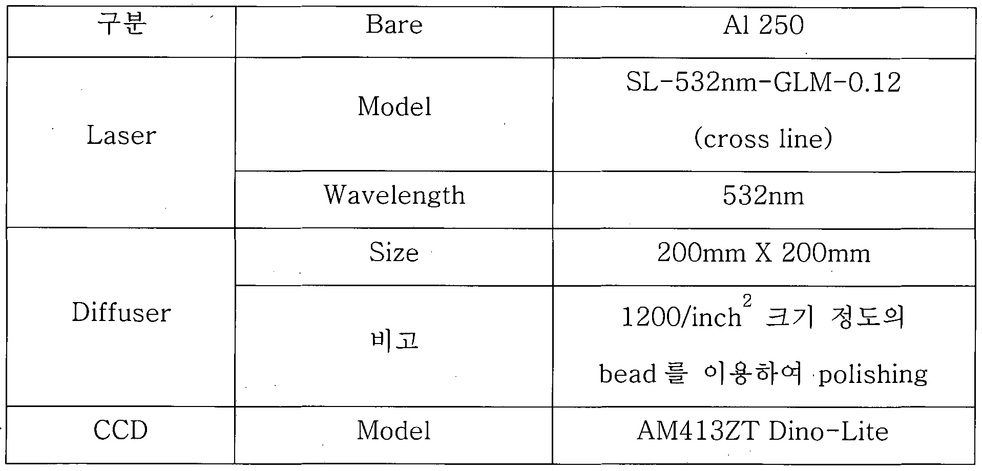
하기 도 7은 암색화층을 포함하지 않는 종래의 전도성 기판의 반사형 회절 이미지를 나타내고 있다. 7 shows a reflective diffraction image of a conventional conductive substrate that does not include a darkening layer.
또한, 본 발명은 터치스크린의 제조방법을 제공한다. In addition, the present invention provides a method of manufacturing a touch screen.
하나의 실시상태에 따르면, 본 발명은 기재 상에 전기 전도성 패턴을 형성 하는 단계를 포함하는 터치스크린의 제조방법을 제공한다. According to one embodiment, the present invention provides a method of manufacturing a touch screen comprising the step of forming an electrically conductive pattern on the substrate.
또 하나의 실시상태에 따르면, 기재 상에 전도성 패턴 형성용 도전층을 형 성하는 단계; 및 상기 도전충을 패터닝하는 단계를 포함하는 터치스크린의 제조방 법을 제공한다. According to yet an embodiment, forming a conductive layer for forming a conductive pattern on the substrate; And it provides a method of manufacturing a touch screen comprising the step of patterning the conductive insect.
상기 제조방법에서는 전술한 각 층의 재료 및 형성방법이 사용될 수 있다. 또한, 본 발명에 따른 터치스크린은 상기 전도성 기판을 포함한다. 예컨대, 정전용량식 터치스크린에 있어서, 상기 본 발명의 일 실시상태에 다른 전도성 기판 은 터치 감웅식 전극 기판으로 사용될 수 있다. In the manufacturing method, the above-described materials and forming methods of the respective layers may be used. In addition, the touch screen according to the present invention includes the conductive substrate. For example, in a capacitive touch screen, another conductive substrate according to the exemplary embodiment of the present invention may be used as a touch sensitive electrode substrate.
본 발명의 일 실시상태에 따른 터치스크린은 하부 기재; 상부 기재; 및 상 기 하부 기재의 상부 기재에 접하는 면 및 상기 상부 기재의 하부 기재에 접하는 면 중 어느 한 면 또는 양면에 구비된 전극층을 포함할 수 있다. 상기 전극층은 각각 X축 위치 검출 및 γ축 위치 검출을 위한 신호 송신 및 수신의 기능을 수행할 수 있다. Touch screen according to an embodiment of the present invention the lower substrate; Upper substrate; And award It may include an electrode layer provided on any one surface or both surfaces of the lower substrate in contact with the upper substrate and the surface in contact with the lower substrate. The electrode layer may perform a function of signal transmission and reception for X-axis position detection and γ-axis position detection, respectively.
이 때, 상기 하부 기재 및 상기 하부 기재의 상부 기재에 접하는 면에 구비 된 전극층; 및 상기 상부 기재 및 상기 상부 기재의 하부 기재에 접하는 면에 구비 된 전극층 중 하나 또는 두 개 모두가 전술한 본 발명의 일 실시상태에 따른 전도 성 기판일 수 있다. 상기 전극층 중 어느 하나만이 본 발명에 따른 전도성 기판인 경우, 나머지 다른 하나는 당 기술분야에 알려져 있는 패턴을 가질 수 있다. At this time, the lower electrode and the electrode layer provided on the surface in contact with the upper substrate of the lower substrate; And one or both of the electrode layer provided on the surface in contact with the upper substrate and the lower substrate of the upper substrate may be a conductive substrate according to an embodiment of the present invention described above. When only one of the electrode layers is the conductive substrate according to the present invention, the other may have a pattern known in the art.
상기 상부 기재와 상기 하부 기재 모두의 일면에 전극층이 구비되어 2층의 전극층이 형성되는 경우, 상기 전극층의 간격을 일정하기 유지하고 접속이 일어나 지 않도록 상기 하부 기재와 상부 기재 사이에 절연층 또는 스페이서가 구비될 수 있다. 상기 절연층은 점착제 또는 UV혹은 열 경화성 수지를 포함할 수 있다. 상기 터치스크린은 전술한 전기 전도성 패턴과 연결된 접지부를 더 포함할 수 있다. 예컨대, 상기 접지부는 상기 기재의 전기 전도성 패턴이 형성된 면의 가 장자리부에 형성될 수 있다. 또한, 상기 전도성 기판을 포함하는 적층재의 적어도 일면에는 반사 방지 필름, 편광 필름, 내지문 필름 중 적어도 하나가 구비될 수 있 다. 설계사양에 따라 전술한 기능성 필름 이외에 다른 종류의 기능성 필름을 더 포 함할 수도 있다. 상기와 같은 터치스크린 이 : D 디스플레이 패널 (OLED Display Panel, PDP), 액정 디스플레이 (Liquid Crystal Display, LCD), 및 음극선관 (Cathode-Ray Tube, CRT), PDP와 같은 디스플레이 장치에 적용될 수 있다. When an electrode layer is provided on one surface of both the upper substrate and the lower substrate to form two electrode layers, an insulating layer or a spacer is provided between the lower substrate and the upper substrate so as to maintain a constant distance between the electrode layers and prevent connection. It may be provided. The insulating layer may include an adhesive or UV or thermosetting resin. The touch screen may further include a ground connected to the aforementioned electrically conductive pattern. For example, the ground portion may be formed at an edge portion of a surface on which the electrically conductive pattern of the substrate is formed. In addition, at least one surface of the laminate including the conductive substrate may be provided with at least one of an anti-reflection film, a polarizing film, a fingerprint. According to design specifications, in addition to the above-described functional film may further include other types of functional film. The touch screen as described above may be applied to display devices such as a D display panel (OLED Display Panel, PDP), a liquid crystal display (LCD), and a cathode-ray tube (CRT) and a PDP.
또한, 본 발명은 상기 터치스크린 및 디스플레이 모들을 포함하는 디스플레 이를 제공한다. The present invention also provides a display comprising the touch screen and display modules.
【발명의 실시를 위한 형태】 [Form for implementation of invention]
이하 실시예를 통하여 본 발명을 더욱 상세하게 설명한다. 그러나, 이하의 실시예는 본 발명을 예시하기 위한 것이며, 이에 의하여 본 발명의 범위가 한정되 는 것은 아니다. The present invention will be described in more detail with reference to the following Examples. However, the following examples are intended to illustrate the invention, whereby the scope of the invention is not limited.
<실시예 > <실시예 i ~ 2> <Example> <Examples i to 2>
본 발명에 따른 불규칙 패턴 형태의 전기 전도성 패턴과 상기 불규칙도가 0인 일반적인 규칙 패턴을 구별하는 방법 중 하나는 단위면적 내 선의 꼭지점의 개수를 확인하는 방법이다. 즉, 폐쇄도형을 이루는 각 꼭지점의 거리가 모두 동일 하지 않으면서 동시에 패턴을 이루는 기본도형의 꼭지점의 개수가, 각 폐쇄도형의 무게중심을 연결하여 형성되는 또 다른 도형의 꼭지점의 개수 대비 약 2배의 차이 가 존재하는 경우를 본 발명에 따른 불규칙 패턴 형태의 전기 전도성 패턴이라 정 의할 수 있다. One of the methods for distinguishing between the electrically conductive pattern in the form of an irregular pattern and the general rule pattern of which the irregularity is 0 is a method of checking the number of vertices of the line in the unit area. In other words, the number of vertices of the basic figure forming the pattern at the same time without the same distance between each vertex of the closed figure is about twice the number of vertices of another figure formed by connecting the center of gravity of each closed figure. When the difference exists can be defined as an electrically conductive pattern of the irregular pattern form according to the present invention.
이러한 차이는 하기 표 2 및 표 3과 같이, 종래의 규칙 패턴과 본 발명에 따른 전기 전도성 패턴의 단위면적 (3.5cm X 3.5cm) 내 존재하는 불규칙도별 다각 형 개수를 비교함으로써 알 수 있다. 즉, 단위 유닛셀이 정사각형인 경우에, 본 발 명에 따른 전기 전도성 패턴의 폐쇄도형은 육각형이 주된 폐쇄도형을 이루게 됨에 따라 꼭지점의 수가 규칙 패턴에 비하여 약 2배로 증가하기 때문이다. This difference can be seen by comparing the number of polygons by irregularity existing in the unit area (3.5 cm X 3.5 cm) of the conventional rule pattern and the electrically conductive pattern according to the present invention, as shown in Table 2 and Table 3 below. That is, in the case where the unit cell is a square, the closed figure of the electrically conductive pattern according to the present invention is because the number of vertices is approximately doubled compared to the regular pattern as the hexagon is the main closed figure.
[표 2] TABLE 2

[표 3] 실시 예 2 TABLE 3 Example 2
다각형 형 Polygon
3각형 4각형 5각형 6각형 7각형 8각형 9각형 10각형 11각형 12각형 개수 태 Triangular Hexagonal Hexagonal Hexagonal Hexagonal Hexagonal Hexagonal 10 Hexagonal Hexagonal 12 Hexagonal
메쉬 - 4761 - - - - ᅳ - - 4761 불규칙도 Mesh-4761----ᅳ--4761 Irregularity
- 233 1280 1989 1069 190 - - - 4761 -233 1280 1989 1069 190---4761
10% 10%
불규칙도 Irregularity
- 178 1248 2011 1135 189 - - ― ᅳ 4761 -178 1248 2011 1135 189---ᅳ 4761
30% 30%
불규칙도 Irregularity
- 168 1273 1981 1105 231 - ― - - 4758 50% -168 1273 1981 1105 231----4758 50%
불규칙도 Irregularity
― 138 1314 1978 1065 244 1 - - 4740 70% 138 314 1978 1065 244 1--4740 70%
볼규칙도 Rules of Ball
5 280 1243 1805 1052 290 42 4 - - 4721 100% 전술한 내용을 기 반으로 하여 , 본 발명에서는 전기 전도성 패턴의 불규칙도 와 실제 모아레 (Moire)가 사라지는 상관관계에 대하여 확인하고자 하였다. 이를 위 하여, 우선 불규칙도에 따른 (꼭지 점간의 거 리 의 표준편차 / 꼭지 점간 거 리 의 평 균)을 확인한 결과 하기 도 1과 같이 불규칙도 35%이상에서는 약 55% 수준으로 수렴하고 있음을 확인할 수 있다. 여 기서, 상기 꼭지 점간의 거 리 (D)는 하기 도 2와 같이 정의될 수 있다. 따라서, (꼭지 점간의 거리의 표준편차 / 꼭지 점간 거리의 평 균)을 고려하는 경우 35%의 불규칙도 이상은 동일한 특성을 지 니고 있음을 확인 할 수 있다. 5 280 1243 1805 1052 290 42 4--4721 100% Based on the above description, in the present invention, the correlation between the irregularity of the electrically conductive pattern and the actual moire disappears. To this end, first of all, the standard deviation of the distance between the vertices / average of the distance between the vertices was determined according to the degree of irregularity. You can check it. Here, the distance (D) between the vertices may be defined as shown in FIG. Therefore, when considering (standard deviation of distance between vertices / average of distance between vertices), it can be confirmed that more than 35% of irregularities have the same characteristics.
〈실시예 3> <Example 3>
또한, 본 발명에서는 전술한 꼭지 점간의 거 리 의 관계와 더불어 단위면적 내 에서 전기 전도성 패턴을 이루고 있는 각 변의 성분들의 각도에 따른 개수 분포를 확인하였다. 그 결과 하기 표 4 및 도 3과 같은 결과를 얻을 수 있었으며, 결과를 통하여 확인할 수 있듯이, 불규칙도 70%이상인 경우에 각도별 선의 개수 분포가 비교적 균등하게 분포하고 있음을 확인할 수 있었다. In addition, in the present invention, the number distribution according to the angle of the components of each side constituting the electrically conductive pattern in the unit area as well as the relationship between the distance between the vertices described above was confirmed. As a result, the results shown in Table 4 and FIG. 3 were obtained, and as can be seen from the results, it was confirmed that the number distribution of lines for each angle was distributed relatively evenly when the irregularity was 70% or more.
[표 4] 불규칙도 TABLE 4 Irregularity
각도 Angle
0 10% 30% 50% 70% 100% 0 10% 30% 50% 70% 100%
0 이상 ~10 미만 4970 2501 2079 1396 1070 8850 and above ~ 10 4970 2501 2079 1396 1070 885
10 이상 ~20 미 만 0 0 414 829 818 82110 or more ~ less than 0 0 0 414 829 818 821
20 이상 ~30 미만 0 0 3 292 710 85220 or more ~ less than 30 0 0 3 292 710 852
30 이상〜 40 미 만 0 7 427 638 666 84330 or more ~ less than 40 0 7 427 638 666 843
40 이상 ~50 미 만 0 2432 1590 1045 868 76140 and over ~ 50 0 0 2432 1590 1045 868 761
50 이상〜 60 미만 0 15 434 616 710 82550 or more ~ less than 60 0 15 434 616 710 825
60 이상〜 70 미만 0 2 1 312 653 81860 or more ~ less than 70 0 2 1 312 653 818
70 이상〜 80 미만 0 0 437 818 833 80370 or more ~ less than 80 0 0 437 818 833 803
80 이상 ~90 미만 0 2501 2073 1456 1101 84780 and above ~ 90 0 250 1 2073 1456 1101 847
90 이상 100 미만 4970 2475 2028 1442 1093 81400 이상〜 110 미만 0 0 432 790 791 853 10 이상 120 미 만 0 1 4 311 687 822 20 이상 130 미 만 0 10 417 655 737 800 30 이상〜 140 미만 0 2408 1612 1015 819 83740 이상〜 150 미만 0 8 409 648 706 854 50 이상 ~ 160 미 만 0 0 1 317 685 76460 이상 170 미만 0 0 435 769 826 80170 이상〜 180 미만 0 2477 2041 1497 1086 844 90 or more Less than 100 4970 2475 2028 1442 1093 81400 or more Less than 110 0 0 432 790 791 853 10 More than 120 Less than 0 1 4 311 687 822 More than 20 More than 130 Less than 0 10 417 655 737 800 More than 30 Less than 140 0 2408 1612 1015 819 83 740 or more ~ less than 150 0 8 409 648 706 854 50 or more ~ less than 160 0 0 1 317 685 76 460 or more but less than 170 0 0 435 769 826 80 170 or more ~ less than 180 0 2477 2041 1497 1086 844
〈실시예 4> <Example 4>
이 러 한 결과를 바탕으로 하여, 본 발명 에서는 불규칙도에 따른 모아레 (Moire) 발생여부를 확인하였으며 (3.5cm χ 3.5cm의 면적 ), 그 결과는 하기 도 8과 같다. 즉, 불규칙도 70% 이상인 경우가 모아레 (Moire) 전방위 에 걸친 모아레 (Moire) 회피 효과가 나타남을 확인하였다. Based on these results, in the present invention it was confirmed whether the moire (Moire) generation according to the irregularity (area of 3.5cm × 3.5cm), the results are as shown in FIG. In other words, it was confirmed that the moire avoidance effect over the entire moire (Moire) when the irregularity is more than 70%.
본 발명에 따른 전도성 기판 및 이를 포함하는 터치스크린은 시 야를 가리 지 않고 전도성이 우수할 뿐만 아니라, 점광원에 의한 반사형 회절 현상을 감 소시킬 수 있으며, 나아가 모아레 (moire) 현상에 의한 디스플레이 화질 저하를 방 지할 수 있다. 또한, 본 발명에 따른 전기 전도성 패턴은 목적하는 패턴을 미리 정 한 후, 간접인쇄법, 포토리소그래피법, 포토그래피법, 하드 (Hard) 마스크를 이용한 방법, 스퍼터링법 등 다양한 방법으로 형성할 수 있으므로, 공정이 용이하고 비용 도 저렴하다. 또한, 본 발명에 따른 전기 전도성 패턴을 이용하는 경우, 불규칙 패 턴의 설계시 인위적으로 불규칙도 등을 조절함으로써 불규칙도의 제어 및 투과율 의 제어가 가능하며, 불규칙도에 상관 없이 동일 피치의 규칙 패턴과 단위면적당 선 밀도가 유사함에 따라 규칙 패턴과 유사한 전기적 균일성을 확보할 수 있다. The conductive substrate and the touch screen including the same according to the present invention points to the field of view. In addition to excellent conductivity, it is possible to reduce reflection diffraction caused by a point light source and to prevent display quality deterioration caused by moire. In addition, the electrically conductive pattern according to the present invention may be formed by various methods such as indirect printing, photolithography, photography, hard mask, sputtering, etc. , Easy to process and low cost. In addition, in the case of using the electrically conductive pattern according to the present invention, it is possible to control the irregularity and control the transmittance by artificially adjusting the irregularity in the design of the irregular pattern, and the regular pattern and the same pitch regardless of the irregularity As the line density per unit area is similar, electrical uniformity similar to the regular pattern can be obtained.
Claims
Priority Applications (3)
| Application Number | Priority Date | Filing Date | Title |
|---|---|---|---|
| CN201280016018.XA CN103477398B (en) | 2011-03-28 | 2012-03-28 | Conductive substrate and touch screen including same |
| JP2014502462A JP5865994B2 (en) | 2011-03-28 | 2012-03-28 | Conductive substrate and touch screen including the same |
| US14/008,201 US9313883B2 (en) | 2011-03-28 | 2012-03-28 | Conductive substrate and touch screen having same |
Applications Claiming Priority (2)
| Application Number | Priority Date | Filing Date | Title |
|---|---|---|---|
| KR20110027832 | 2011-03-28 | ||
| KR10-2011-0027832 | 2011-03-28 |
Publications (2)
| Publication Number | Publication Date |
|---|---|
| WO2012134175A2 true WO2012134175A2 (en) | 2012-10-04 |
| WO2012134175A3 WO2012134175A3 (en) | 2013-01-03 |
Family
ID=46932125
Family Applications (2)
| Application Number | Title | Priority Date | Filing Date |
|---|---|---|---|
| PCT/KR2012/002285 Ceased WO2012134175A2 (en) | 2011-03-28 | 2012-03-28 | Conductive substrate and touchscreen having same |
| PCT/KR2012/002283 Ceased WO2012134173A2 (en) | 2011-03-28 | 2012-03-28 | Conductive substrate and touchscreen having same |
Family Applications After (1)
| Application Number | Title | Priority Date | Filing Date |
|---|---|---|---|
| PCT/KR2012/002283 Ceased WO2012134173A2 (en) | 2011-03-28 | 2012-03-28 | Conductive substrate and touchscreen having same |
Country Status (6)
| Country | Link |
|---|---|
| US (2) | US9313883B2 (en) |
| JP (3) | JP5865994B2 (en) |
| KR (2) | KR101385834B1 (en) |
| CN (2) | CN103597427B (en) |
| TW (3) | TWI511168B (en) |
| WO (2) | WO2012134175A2 (en) |
Cited By (3)
| Publication number | Priority date | Publication date | Assignee | Title |
|---|---|---|---|---|
| JP2014119764A (en) * | 2012-12-17 | 2014-06-30 | Lg Innotek Co Ltd | Method of designing random pattern |
| WO2015048828A1 (en) * | 2013-10-04 | 2015-04-09 | Plansee Se | Touch sensor arrangement |
| JP2016540304A (en) * | 2013-12-13 | 2016-12-22 | エルジー・ケム・リミテッド | TOUCH SENSOR AND METHOD FOR MANUFACTURING THE SAME {TOUCH SENSOR AND METHOD THE FOR MANUFACTURING SAME} |
Families Citing this family (22)
| Publication number | Priority date | Publication date | Assignee | Title |
|---|---|---|---|---|
| CN104603886B (en) | 2012-08-31 | 2016-12-07 | Lg化学株式会社 | Conductive structure and manufacturing method thereof |
| KR101388699B1 (en) * | 2012-11-22 | 2014-04-24 | 삼성전기주식회사 | Method and apparatus for sensing touch input |
| KR102153428B1 (en) * | 2013-02-20 | 2020-09-08 | 도오쿄 인스티튜드 오브 테크놀로지 | Electroconductive Nanowire Network, and Electroconductive Substrate and Transparent Electrode Using Same, and Method for Manufacturing Electroconductive Nanowire Network, Electroconductive Substrate, and Transparent electrode |
| US9790126B2 (en) * | 2013-09-05 | 2017-10-17 | Apple Inc. | Opaque color stack for electronic device |
| JP6277262B2 (en) * | 2014-03-13 | 2018-02-07 | 株式会社ノリタケカンパニーリミテド | Projected capacitive touch switch panel |
| KR20160028838A (en) * | 2014-09-04 | 2016-03-14 | 주식회사 엘지화학 | Touch screen and method for preparing the same |
| KR101743329B1 (en) * | 2014-09-04 | 2017-06-15 | 주식회사 엘지화학 | Touch screen and method for preparing the same |
| US10732771B2 (en) | 2014-11-12 | 2020-08-04 | Shenzhen GOODIX Technology Co., Ltd. | Fingerprint sensors having in-pixel optical sensors |
| JP6447185B2 (en) * | 2015-01-30 | 2019-01-09 | 住友金属鉱山株式会社 | Method for manufacturing conductive substrate, method for manufacturing laminated conductive substrate |
| US10459547B2 (en) * | 2015-02-26 | 2019-10-29 | Lg Chem, Ltd | Conductive structure and method for manufacturing same |
| KR20160115588A (en) * | 2015-03-27 | 2016-10-06 | 주식회사 엘지화학 | Display device and method for manufacturing the same |
| EP3278272B1 (en) | 2015-06-18 | 2020-12-09 | Shenzhen Goodix Technology Co., Ltd. | Multifunction fingerprint sensor having optical sensing capability |
| CN107004130B (en) | 2015-06-18 | 2020-08-28 | 深圳市汇顶科技股份有限公司 | Optical sensor module under screen for sensing fingerprint on screen |
| US10410037B2 (en) | 2015-06-18 | 2019-09-10 | Shenzhen GOODIX Technology Co., Ltd. | Under-screen optical sensor module for on-screen fingerprint sensing implementing imaging lens, extra illumination or optical collimator array |
| US10410033B2 (en) | 2015-06-18 | 2019-09-10 | Shenzhen GOODIX Technology Co., Ltd. | Under-LCD screen optical sensor module for on-screen fingerprint sensing |
| US10437974B2 (en) | 2015-06-18 | 2019-10-08 | Shenzhen GOODIX Technology Co., Ltd. | Optical sensing performance of under-screen optical sensor module for on-screen fingerprint sensing |
| TWI626578B (en) * | 2016-12-19 | 2018-06-11 | 恆顥科技股份有限公司 | Touch panel |
| CN108205392A (en) | 2016-12-19 | 2018-06-26 | 恒颢科技股份有限公司 | Touch panel |
| US10614283B2 (en) | 2017-03-07 | 2020-04-07 | Shenzhen GOODIX Technology Co., Ltd. | Devices with peripheral task bar display zone and under-LCD screen optical sensor module for on-screen fingerprint sensing |
| US10331939B2 (en) * | 2017-07-06 | 2019-06-25 | Shenzhen GOODIX Technology Co., Ltd. | Multi-layer optical designs of under-screen optical sensor module having spaced optical collimator array and optical sensor array for on-screen fingerprint sensing |
| WO2019172423A1 (en) * | 2018-03-09 | 2019-09-12 | 大日本印刷株式会社 | Electroconductive film, sensor, touch panel, and image display device |
| KR102822260B1 (en) * | 2019-12-31 | 2025-06-18 | 미래나노텍(주) | Screen apparatus |
Family Cites Families (36)
| Publication number | Priority date | Publication date | Assignee | Title |
|---|---|---|---|---|
| JP2003195356A (en) | 1997-10-31 | 2003-07-09 | Seiko Epson Corp | Liquid crystal device, electronic device, and projection display device |
| JP4090546B2 (en) | 1997-11-14 | 2008-05-28 | 大日本印刷株式会社 | Electromagnetic shielding plate |
| JP3311720B2 (en) * | 1999-01-22 | 2002-08-05 | 三井化学株式会社 | Display filter |
| JP2002014772A (en) * | 2000-06-30 | 2002-01-18 | Minolta Co Ltd | Touch panel, display panel, and display device |
| JP2002108248A (en) | 2000-07-26 | 2002-04-10 | Seiko Epson Corp | Electro-optical device, substrate for electro-optical device, and projection display device |
| KR100709985B1 (en) * | 2005-01-04 | 2007-04-23 | 삼성코닝 주식회사 | Filter for display device and display device including same |
| JP4610416B2 (en) * | 2005-06-10 | 2011-01-12 | 日本写真印刷株式会社 | Capacitive touch panel |
| TWM290361U (en) * | 2005-10-14 | 2006-05-01 | Egbn Electronics Ltd | Electric conductive substrate |
| JP2007155871A (en) | 2005-12-01 | 2007-06-21 | Epson Imaging Devices Corp | Electrooptical device, method for manufacturing electrooptical device, and electronic apparatus |
| TWI327238B (en) * | 2005-12-28 | 2010-07-11 | Au Optronics Corp | Conductive substrate of liquid crystal display and method for manufacturing the same |
| JP2007227906A (en) * | 2006-01-25 | 2007-09-06 | Toray Ind Inc | Conductive substrate and method for manufacturing the same |
| WO2007114076A1 (en) | 2006-04-05 | 2007-10-11 | Toray Industries, Inc. | Method for producing conductive substrate and conductive substrate |
| DE102006052622A1 (en) * | 2006-11-08 | 2008-05-15 | Braun Gmbh | Shaving foil for an electric shaver |
| JP4783721B2 (en) * | 2006-12-08 | 2011-09-28 | 大日本印刷株式会社 | Metal blackening method, electromagnetic wave shielding filter, composite filter, and display |
| JP4927159B2 (en) | 2007-03-01 | 2012-05-09 | シャープ株式会社 | Display panel substrate, display panel, display device, and display panel substrate manufacturing method |
| EP2154940A4 (en) | 2007-05-09 | 2012-01-25 | Toray Industries | Conductive board, electromagnetic shielding board for plasma display and method for manufacturing conductive board |
| JP5429584B2 (en) | 2007-09-26 | 2014-02-26 | Nltテクノロジー株式会社 | Display device, portable device using the same, and terminal device |
| US8068195B2 (en) | 2008-01-14 | 2011-11-29 | Lg Electronics Inc. | Portable device including external-light-shielding sheet |
| KR100938682B1 (en) | 2008-01-14 | 2010-01-25 | 엘지전자 주식회사 | Touch panel and display device having same |
| JP2009259063A (en) * | 2008-04-18 | 2009-11-05 | Gunze Ltd | Touch panel and its production method |
| JP5788129B2 (en) * | 2008-07-18 | 2015-09-30 | 日東電工株式会社 | Transparent conductive film and touch panel |
| KR100991610B1 (en) * | 2008-08-28 | 2010-11-04 | 호서대학교 산학협력단 | Method for manufacturing thin film for black matrix and thus thin film for black matrix |
| US9999099B2 (en) | 2009-01-21 | 2018-06-12 | Lg Chem, Ltd. | Heating element and a manufacturing method thereof |
| WO2010090487A2 (en) * | 2009-02-06 | 2010-08-12 | 주식회사 엘지화학 | Touch screen and manufacturing method thereof |
| CN102308366B (en) * | 2009-02-06 | 2015-08-12 | Lg化学株式会社 | Touch-screen and preparation method thereof |
| JP2010198615A (en) * | 2009-02-20 | 2010-09-09 | Acrosense Technology Co Ltd | Capacitive touch panel |
| JPWO2010101028A1 (en) * | 2009-03-02 | 2012-09-06 | 東レ株式会社 | Reticulated metal fine particle laminated film and method for producing the same |
| KR20100122315A (en) | 2009-05-12 | 2010-11-22 | 제일모직주식회사 | Pattern structure of prism film for reducing moire |
| KR20100128388A (en) | 2009-05-28 | 2010-12-08 | 한국전자통신연구원 | Optical touch screen |
| TWI550649B (en) | 2009-07-16 | 2016-09-21 | Lg化學股份有限公司 | Electrical conductor and preparation method thereof |
| WO2011008055A2 (en) * | 2009-07-16 | 2011-01-20 | 주식회사 엘지화학 | Electrical conductor and a production method therefor |
| KR101811068B1 (en) * | 2009-12-28 | 2017-12-20 | 도레이 카부시키가이샤 | Conductive laminated body and touch panel using the same |
| WO2011125597A1 (en) * | 2010-03-31 | 2011-10-13 | 富士フイルム株式会社 | Conductive film manufacturing method, conductive film, and recording medium |
| JP5248653B2 (en) | 2010-05-27 | 2013-07-31 | 富士フイルム株式会社 | Conductive sheet and capacitive touch panel |
| KR101367569B1 (en) * | 2010-12-29 | 2014-02-28 | 주식회사 엘지화학 | Touch screen and method for manufacturing the same |
| CN103636285B (en) * | 2012-04-23 | 2016-08-17 | Lg化学株式会社 | Heating element and method of manufacturing the same |
-
2012
- 2012-03-28 WO PCT/KR2012/002285 patent/WO2012134175A2/en not_active Ceased
- 2012-03-28 TW TW101110880A patent/TWI511168B/en active
- 2012-03-28 US US14/008,201 patent/US9313883B2/en active Active
- 2012-03-28 US US14/008,522 patent/US9363888B2/en active Active
- 2012-03-28 TW TW103129844A patent/TW201506738A/en unknown
- 2012-03-28 CN CN201280015861.6A patent/CN103597427B/en active Active
- 2012-03-28 JP JP2014502462A patent/JP5865994B2/en active Active
- 2012-03-28 WO PCT/KR2012/002283 patent/WO2012134173A2/en not_active Ceased
- 2012-03-28 KR KR1020120031786A patent/KR101385834B1/en active Active
- 2012-03-28 KR KR1020120031782A patent/KR101385898B1/en active Active
- 2012-03-28 JP JP2014502460A patent/JP6070690B2/en active Active
- 2012-03-28 TW TW101110881A patent/TWI463370B/en active
- 2012-03-28 CN CN201280016018.XA patent/CN103477398B/en active Active
-
2016
- 2016-01-08 JP JP2016003073A patent/JP6529443B2/en active Active
Cited By (3)
| Publication number | Priority date | Publication date | Assignee | Title |
|---|---|---|---|---|
| JP2014119764A (en) * | 2012-12-17 | 2014-06-30 | Lg Innotek Co Ltd | Method of designing random pattern |
| WO2015048828A1 (en) * | 2013-10-04 | 2015-04-09 | Plansee Se | Touch sensor arrangement |
| JP2016540304A (en) * | 2013-12-13 | 2016-12-22 | エルジー・ケム・リミテッド | TOUCH SENSOR AND METHOD FOR MANUFACTURING THE SAME {TOUCH SENSOR AND METHOD THE FOR MANUFACTURING SAME} |
Also Published As
| Publication number | Publication date |
|---|---|
| JP6070690B2 (en) | 2017-02-01 |
| JP2014517368A (en) | 2014-07-17 |
| KR101385834B1 (en) | 2014-04-21 |
| JP2014515141A (en) | 2014-06-26 |
| KR101385898B1 (en) | 2014-04-16 |
| US20140022739A1 (en) | 2014-01-23 |
| KR20120110067A (en) | 2012-10-09 |
| TWI463370B (en) | 2014-12-01 |
| TW201306058A (en) | 2013-02-01 |
| CN103597427A (en) | 2014-02-19 |
| CN103597427B (en) | 2016-08-17 |
| US20140016047A1 (en) | 2014-01-16 |
| KR20120110066A (en) | 2012-10-09 |
| WO2012134173A8 (en) | 2012-11-29 |
| JP2016076270A (en) | 2016-05-12 |
| JP5865994B2 (en) | 2016-02-17 |
| TW201506738A (en) | 2015-02-16 |
| WO2012134175A3 (en) | 2013-01-03 |
| JP6529443B2 (en) | 2019-06-12 |
| WO2012134173A3 (en) | 2013-02-14 |
| CN103477398B (en) | 2016-12-07 |
| CN103477398A (en) | 2013-12-25 |
| US9363888B2 (en) | 2016-06-07 |
| TWI511168B (en) | 2015-12-01 |
| TW201305872A (en) | 2013-02-01 |
| WO2012134173A2 (en) | 2012-10-04 |
| US9313883B2 (en) | 2016-04-12 |
Similar Documents
| Publication | Publication Date | Title |
|---|---|---|
| KR101385834B1 (en) | Conducting substrate and touch screen comprising the same | |
| KR101306563B1 (en) | Conductive structure body and method for manufacturing the same | |
| CN104584143B (en) | Conductive structure and the method manufacturing this conductive structure | |
| KR101224282B1 (en) | Conductive structure body and method for preparing the same | |
| EP3073353B1 (en) | Conductive structure and manufacturing method therefor | |
| WO2012161462A2 (en) | Conductive substrate and touch panel comprising same | |
| US11099695B2 (en) | Touch panel | |
| KR102100534B1 (en) | Conductive structure body and method for manufacturing the same | |
| KR101927258B1 (en) | Conductive structure body and method for manufacturing the same |
Legal Events
| Date | Code | Title | Description |
|---|---|---|---|
| 121 | Ep: the epo has been informed by wipo that ep was designated in this application |
Ref document number: 12764149 Country of ref document: EP Kind code of ref document: A2 |
|
| ENP | Entry into the national phase |
Ref document number: 2014502462 Country of ref document: JP Kind code of ref document: A |
|
| WWE | Wipo information: entry into national phase |
Ref document number: 14008201 Country of ref document: US |
|
| NENP | Non-entry into the national phase |
Ref country code: DE |
|
| 122 | Ep: pct application non-entry in european phase |
Ref document number: 12764149 Country of ref document: EP Kind code of ref document: A2 |