WO2012137497A1 - Substrat pour élément de conversion photoélectrique ayant une électrode en molybdène, élément de conversion photoélectrique et cellule solaire - Google Patents
Substrat pour élément de conversion photoélectrique ayant une électrode en molybdène, élément de conversion photoélectrique et cellule solaire Download PDFInfo
- Publication number
- WO2012137497A1 WO2012137497A1 PCT/JP2012/002354 JP2012002354W WO2012137497A1 WO 2012137497 A1 WO2012137497 A1 WO 2012137497A1 JP 2012002354 W JP2012002354 W JP 2012002354W WO 2012137497 A1 WO2012137497 A1 WO 2012137497A1
- Authority
- WO
- WIPO (PCT)
- Prior art keywords
- photoelectric conversion
- substrate
- conversion element
- alkali metal
- group
- Prior art date
- Legal status (The legal status is an assumption and is not a legal conclusion. Google has not performed a legal analysis and makes no representation as to the accuracy of the status listed.)
- Ceased
Links
Images


Classifications
-
- C—CHEMISTRY; METALLURGY
- C23—COATING METALLIC MATERIAL; COATING MATERIAL WITH METALLIC MATERIAL; CHEMICAL SURFACE TREATMENT; DIFFUSION TREATMENT OF METALLIC MATERIAL; COATING BY VACUUM EVAPORATION, BY SPUTTERING, BY ION IMPLANTATION OR BY CHEMICAL VAPOUR DEPOSITION, IN GENERAL; INHIBITING CORROSION OF METALLIC MATERIAL OR INCRUSTATION IN GENERAL
- C23C—COATING METALLIC MATERIAL; COATING MATERIAL WITH METALLIC MATERIAL; SURFACE TREATMENT OF METALLIC MATERIAL BY DIFFUSION INTO THE SURFACE, BY CHEMICAL CONVERSION OR SUBSTITUTION; COATING BY VACUUM EVAPORATION, BY SPUTTERING, BY ION IMPLANTATION OR BY CHEMICAL VAPOUR DEPOSITION, IN GENERAL
- C23C28/00—Coating for obtaining at least two superposed coatings either by methods not provided for in a single one of groups C23C2/00 - C23C26/00 or by combinations of methods provided for in subclasses C23C and C25C or C25D
- C23C28/04—Coating for obtaining at least two superposed coatings either by methods not provided for in a single one of groups C23C2/00 - C23C26/00 or by combinations of methods provided for in subclasses C23C and C25C or C25D only coatings of inorganic non-metallic material
-
- C—CHEMISTRY; METALLURGY
- C23—COATING METALLIC MATERIAL; COATING MATERIAL WITH METALLIC MATERIAL; CHEMICAL SURFACE TREATMENT; DIFFUSION TREATMENT OF METALLIC MATERIAL; COATING BY VACUUM EVAPORATION, BY SPUTTERING, BY ION IMPLANTATION OR BY CHEMICAL VAPOUR DEPOSITION, IN GENERAL; INHIBITING CORROSION OF METALLIC MATERIAL OR INCRUSTATION IN GENERAL
- C23C—COATING METALLIC MATERIAL; COATING MATERIAL WITH METALLIC MATERIAL; SURFACE TREATMENT OF METALLIC MATERIAL BY DIFFUSION INTO THE SURFACE, BY CHEMICAL CONVERSION OR SUBSTITUTION; COATING BY VACUUM EVAPORATION, BY SPUTTERING, BY ION IMPLANTATION OR BY CHEMICAL VAPOUR DEPOSITION, IN GENERAL
- C23C30/00—Coating with metallic material characterised only by the composition of the metallic material, i.e. not characterised by the coating process
-
- C—CHEMISTRY; METALLURGY
- C25—ELECTROLYTIC OR ELECTROPHORETIC PROCESSES; APPARATUS THEREFOR
- C25D—PROCESSES FOR THE ELECTROLYTIC OR ELECTROPHORETIC PRODUCTION OF COATINGS; ELECTROFORMING; APPARATUS THEREFOR
- C25D11/00—Electrolytic coating by surface reaction, i.e. forming conversion layers
- C25D11/02—Anodisation
- C25D11/04—Anodisation of aluminium or alloys based thereon
- C25D11/18—After-treatment, e.g. pore-sealing
- C25D11/24—Chemical after-treatment
-
- H—ELECTRICITY
- H10—SEMICONDUCTOR DEVICES; ELECTRIC SOLID-STATE DEVICES NOT OTHERWISE PROVIDED FOR
- H10F—INORGANIC SEMICONDUCTOR DEVICES SENSITIVE TO INFRARED RADIATION, LIGHT, ELECTROMAGNETIC RADIATION OF SHORTER WAVELENGTH OR CORPUSCULAR RADIATION
- H10F77/00—Constructional details of devices covered by this subclass
- H10F77/10—Semiconductor bodies
- H10F77/16—Material structures, e.g. crystalline structures, film structures or crystal plane orientations
- H10F77/169—Thin semiconductor films on metallic or insulating substrates
- H10F77/1698—Thin semiconductor films on metallic or insulating substrates the metallic or insulating substrates being flexible
- H10F77/1699—Thin semiconductor films on metallic or insulating substrates the metallic or insulating substrates being flexible the films including Group I-III-VI materials, e.g. CIS or CIGS on metal foils or polymer foils
-
- C—CHEMISTRY; METALLURGY
- C25—ELECTROLYTIC OR ELECTROPHORETIC PROCESSES; APPARATUS THEREFOR
- C25D—PROCESSES FOR THE ELECTROLYTIC OR ELECTROPHORETIC PRODUCTION OF COATINGS; ELECTROFORMING; APPARATUS THEREFOR
- C25D11/00—Electrolytic coating by surface reaction, i.e. forming conversion layers
- C25D11/02—Anodisation
- C25D11/04—Anodisation of aluminium or alloys based thereon
- C25D11/06—Anodisation of aluminium or alloys based thereon characterised by the electrolytes used
- C25D11/08—Anodisation of aluminium or alloys based thereon characterised by the electrolytes used containing inorganic acids
-
- C—CHEMISTRY; METALLURGY
- C25—ELECTROLYTIC OR ELECTROPHORETIC PROCESSES; APPARATUS THEREFOR
- C25D—PROCESSES FOR THE ELECTROLYTIC OR ELECTROPHORETIC PRODUCTION OF COATINGS; ELECTROFORMING; APPARATUS THEREFOR
- C25D11/00—Electrolytic coating by surface reaction, i.e. forming conversion layers
- C25D11/02—Anodisation
- C25D11/04—Anodisation of aluminium or alloys based thereon
- C25D11/06—Anodisation of aluminium or alloys based thereon characterised by the electrolytes used
- C25D11/10—Anodisation of aluminium or alloys based thereon characterised by the electrolytes used containing organic acids
-
- Y—GENERAL TAGGING OF NEW TECHNOLOGICAL DEVELOPMENTS; GENERAL TAGGING OF CROSS-SECTIONAL TECHNOLOGIES SPANNING OVER SEVERAL SECTIONS OF THE IPC; TECHNICAL SUBJECTS COVERED BY FORMER USPC CROSS-REFERENCE ART COLLECTIONS [XRACs] AND DIGESTS
- Y02—TECHNOLOGIES OR APPLICATIONS FOR MITIGATION OR ADAPTATION AGAINST CLIMATE CHANGE
- Y02E—REDUCTION OF GREENHOUSE GAS [GHG] EMISSIONS, RELATED TO ENERGY GENERATION, TRANSMISSION OR DISTRIBUTION
- Y02E10/00—Energy generation through renewable energy sources
- Y02E10/50—Photovoltaic [PV] energy
- Y02E10/541—CuInSe2 material PV cells
Definitions
- the present invention relates to a photoelectric conversion element suitable for uses such as a substrate for a photoelectric conversion element with a molybdenum electrode and a solar battery, and a solar battery.
- a photoelectric conversion element having a laminated structure of a lower electrode (back electrode), a photoelectric conversion layer that generates current by light absorption, and an upper electrode (transparent electrode) on a substrate is used for applications such as solar cells.
- back electrode lower electrode
- photoelectric conversion layer that generates current by light absorption
- upper electrode transparent electrode
- solar cells Si-based solar cells using bulk single-crystal Si or polycrystalline Si, or thin-film amorphous Si have been mainstream, but in recent years, research and development of compound semiconductor-based solar cells that do not depend on Si have been conducted. Has been made.
- a thin film system such as a CIS (Cu—In—Se) system or a CIGS (Cu—In—Ga—Se) system composed of an Ib group element, an IIIb group element, and a VIb group element is used. It is known that the photoelectric conversion efficiency is high.
- the alkalinity preferably Na
- the crystallinity of the photoelectric conversion layer is improved and the photoelectric conversion efficiency is improved.
- Patent Documents 1 and 2 Conventionally, Na is diffused into the photoelectric conversion layer using a soda-lime glass substrate containing Na.
- Patent Document 3 discloses applying alkali metal silicate, specifically sodium silicate, by liquid phase application.
- Patent Document 4 discloses that an anodized substrate is brought into contact with a sodium hydroxide aqueous solution and doped with sodium.
- Patent Document 5 describes that a silicon oxide film is formed on a stainless steel substrate by a sol-gel method, and an insulating layer is further formed of a material containing Na.
- Non-Patent Documents 1 and 2 it is known that lithium, potassium, and cesium, which are alkali metals other than sodium, are less in amount that can be added to CIGS than sodium, and even if added, the effect of improving photoelectric conversion efficiency is low ( Non-Patent Documents 1 and 2).
- the present invention has been made in view of the above circumstances, and is capable of efficiently diffusing alkali metal ions into the photoelectric conversion semiconductor layer, and can increase the photoelectric conversion efficiency of the photoelectric conversion element.
- An object of the present invention is to provide an element substrate, a photoelectric conversion element, and a solar cell.
- the substrate for a photoelectric conversion element with a molybdenum electrode according to the first aspect of the present invention is a photoelectric conversion element in which an alkali metal silicate layer containing lithium silicate or potassium silicate and sodium silicate is laminated on the substrate. And a molybdenum electrode laminated on the alkali metal silicate layer.
- the molar ratio of lithium or potassium to silicon in the alkali metal silicate layer in the first embodiment is preferably 0.001 or more and 1 or less.
- the sum of the molar ratio of lithium or potassium to silicon and the molar ratio of sodium to silicon in the first embodiment is preferably 1 or less.
- the alkali metal silicate layer in the first embodiment preferably contains boron or phosphorus.
- the thickness of the alkali metal silicate layer in the first embodiment is preferably 2 ⁇ m or less.
- the substrate in the first aspect is preferably a metal substrate.
- An anodized aluminum film is preferably formed on the surface of the metal substrate.
- the metal substrate is preferably a clad material in which one or both surfaces of aluminum, stainless steel, or steel plate are integrated with an aluminum plate.
- the anodized aluminum film is a porous anodized aluminum film, and the porous anodized aluminum film preferably has a compressive stress.
- the photoelectric conversion element of the present invention can be formed on the photoelectric conversion element substrate of the first aspect.
- the photoelectric conversion element substrate according to the second aspect of the present invention includes, on the substrate, at least one of group 13 elements excluding aluminum or group 15 element excluding nitrogen, silicon, and an alkali metal, and is a liquid phase method. And an molybdenum metal electrode laminated on the alkali metal silicate layer. .
- the group 13 element excluding aluminum or the group 15 element excluding nitrogen is preferably boron or phosphorus.
- the alkali metal in the second embodiment is preferably sodium. More preferably, the alkali metal in the second embodiment includes two kinds of lithium or potassium and sodium.
- the total molar ratio of the group 13 element excluding aluminum or the group 15 element excluding nitrogen to silicon is more preferably 0.15 or less.
- the thickness of the alkali metal silicate layer in the second embodiment is preferably 2 ⁇ m or less.
- the substrate in the second aspect is more preferably a metal substrate. It is more preferable that an anodized aluminum film is formed on the surface of the metal substrate.
- the metal substrate is more preferably a clad material in which one or both surfaces of aluminum, stainless steel, or steel plate are integrated with an aluminum plate.
- the photoelectric conversion element of the present invention can be formed on the photoelectric conversion element substrate of the second aspect.
- the photoelectric conversion element of the present invention is a photoelectric conversion element in which a molybdenum electrode, a photoelectric conversion semiconductor layer, and an upper electrode are sequentially stacked on a substrate, and the main component of the photoelectric conversion semiconductor layer is Ib.
- the content of each of lithium ions or potassium ions and sodium ions contained in the photoelectric conversion semiconductor layer is preferably 1 ⁇ 10 15 atms / cm 3 or more.
- the lithium ion or potassium ion and sodium ion contained in the photoelectric conversion semiconductor layer are preferably supplied from an alkali supply layer formed between the substrate and the molybdenum electrode.
- the main components of the photoelectric conversion semiconductor layer are at least one Ib group element selected from the group consisting of Cu and Ag, at least one IIIb group element selected from the group consisting of Al, Ga and In, and S , Se, and Te are preferably at least one compound semiconductor composed of at least one VIb group element selected from the group consisting of:
- the substrate is preferably a metal substrate.
- An anodized aluminum film is preferably formed on the surface of the metal substrate.
- the metal substrate is preferably a clad material in which one or both surfaces of aluminum, stainless steel, or steel plate are integrated with an aluminum plate.
- the anodized aluminum film is a porous anodized aluminum film, and the porous anodized aluminum film preferably has a compressive stress.
- the solar cell of this invention can be equipped with said photoelectric conversion element.
- the photoelectric conversion element substrate of the first aspect of the present invention has an alkali metal silicate layer containing an alkali metal silicate (wherein the alkali metal is other than sodium) and sodium silicate, and is separate from sodium. Even when an electrode made of molybdenum is formed on the alkali metal silicate layer by using together with the alkali metal, sodium reacts with molybdenum to generate impurities, or sodium is eluted by washing with water. Therefore, sodium in the alkali metal silicate layer can be efficiently diffused into the photoelectric conversion semiconductor layer, and the power generation efficiency of the photoelectric conversion element can be improved.
- the substrate for photoelectric conversion elements of the second aspect of the present invention contains at least one of group 13 elements excluding aluminum or group 15 elements excluding nitrogen in the alkali metal silicate layer, the alkali metal silicate layer Even if an electrode made of molybdenum is formed on the surface, it is possible to prevent foreign metals from reacting with sodium and molybdenum, and elution of alkali metal by washing with water. Metal can be efficiently diffused into the photoelectric conversion semiconductor layer, and the power generation efficiency of the photoelectric conversion element can be improved.
- the alkali metal silicate layer contains at least one of group 13 elements excluding aluminum or group 15 elements excluding nitrogen, the mechanism of action for obtaining such an effect is not necessarily clear. The mechanism is estimated.
- an alkali metal silicate layer consisting only of silicon, alkali metal and oxygen
- the alkali metal ions are dissolved in the glass, but the alkali metal ions are monovalent. Do not form. For this reason, the alkali metal has insufficient interaction with oxygen, is liberated from the glass, and easily segregates on the surface.
- the alkali metal ions are segregated on the surface, there arises a problem that when the electrode is provided, it reacts with sputtered molybdenum having high energy to generate foreign matter.
- oxides of Group 13 elements excluding aluminum or Group 15 elements excluding nitrogen are known to be dissolved in silicate glass to form a single-phase glass. Also in the silicate layer, by adding a group 13 element excluding aluminum or a group 15 element excluding nitrogen, ions of these elements are taken into a glass network composed of silicon-oxygen to form a uniform glass.
- the microscopic structure of the glass has changed and the stability of alkali metal ions in the glass has improved, so the release of alkali metal ions is suppressed and segregation of alkali metal ions to the surface is prevented. It is presumed that the generation of foreign matters during molybdenum sputtering can be prevented without occurring. Moreover, since segregation to the surface of alkali metal ions is suppressed, it is presumed that alkali metal ion elution by water washing is also reduced.
- the photoelectric conversion element of the present invention can improve the power generation efficiency of the photoelectric conversion element by including lithium ions or potassium ions in addition to sodium ions in the photoelectric conversion semiconductor layer.
- the mechanism of action in which characteristics are improved by combining lithium ions or potassium ions with sodium ions is not always clear.
- the photoelectric conversion semiconductor layer containing lithium ions or potassium ions in addition to sodium ions and the photoelectric conversion semiconductor layer containing only sodium ions are included in the photoelectric conversion semiconductor layer.
- the amount of sodium added is almost the same. From this, although the influence on the physical properties and characteristics of the photoelectric conversion semiconductor layer is not clear, it is presumed that the presence of lithium ions or potassium ions contributes to the improvement of photoelectric conversion efficiency. This was first discovered by the inventor.
- the photoelectric conversion element substrate of the first aspect of the present invention will be described in detail.
- the alkali metal silicate layer in the substrate for a photoelectric conversion element of the first aspect includes lithium silicate or potassium silicate and sodium silicate. Lithium silicate and potassium silicate may contain both.
- the molar ratio of lithium or potassium to silicon in the alkali metal silicate layer is preferably from 0.001 to 1, more preferably from 0.01 to 1, more preferably from 0.02 to 1, particularly preferably. Is preferably from 0.05 to 0.5.
- Silicon is the total silicon contained in the alkali metal silicate layer (including silicon derived from sodium silicate). When both lithium silicate and potassium silicate are included, lithium silicate derived, potassium silicate derived , And the molar ratio of the sum of lithium and potassium to silicon from sodium silicate. When the molar ratio of lithium or potassium to silicon is larger than 1, lithium or potassium becomes too much and it becomes difficult to solidify as a silicate. On the other hand, when the molar ratio of lithium or potassium to silicon is less than 0.001, the effect of addition cannot be obtained due to too little lithium or potassium, and the photoelectric conversion efficiency of the photoelectric conversion element does not increase.
- the sum of the molar ratio of lithium or potassium to the total silicon contained in the alkali metal silicate layer and the molar ratio of sodium to the total silicon contained in the alkali metal silicate layer is preferably 1 or less, more preferably Is desirably 0.8 or less. If lithium or potassium is not contained, the insulating property is lowered, and, in addition, impurities are formed when a molybdenum film generally used for the back electrode is formed, so that the power generation efficiency is lowered. This is presumed to be due to the high water absorption of sodium. On the other hand, power generation efficiency cannot be increased only with lithium or potassium.
- Known methods for producing sodium silicate, lithium silicate, and potassium silicate include wet methods and dry methods. Silicon oxide is dissolved in sodium hydroxide, lithium hydroxide, and potassium hydroxide, respectively. Can be produced. In addition, alkali metal silicates having various molar ratios are commercially available and can be used.
- lithium silicate As sodium silicate, lithium silicate, and potassium silicate, various molar ratios of sodium silicate, lithium silicate, and potassium silicate are commercially available.
- the SiO 2 / A 2 O (A: alkali metal) molar ratio is often used as an index indicating the ratio of silicon and alkali metal.
- lithium silicate there are lithium silicate 35, lithium silicate 45, lithium silicate 75, etc. manufactured by Nissan Chemical Industries, Ltd.
- potassium silicate No. 1 potassium silicate, No. 2 potassium silicate and the like are commercially available.
- sodium silicate sodium orthosilicate, sodium metasilicate, No. 1 sodium silicate, No. 2 sodium silicate, No. 3 sodium silicate, No. 4 sodium silicate, etc. are known, and the molar ratio of silicon is up to several tens. Elevated high mol sodium silicate is also commercially available.
- a solution having an arbitrary concentration can be obtained by mixing the above sodium silicate, lithium silicate, and potassium silicate with water in an arbitrary ratio.
- the ratio of lithium or potassium to silicon can be changed by mixing these alkali metal silicates, and can also be changed by mixing various sodium silicates in an arbitrary ratio.
- the viscosity of the coating solution can be adjusted to determine appropriate coating conditions.
- a doctor blade method, a wire bar method, a gravure method, a spray method, a dip coating method, a spin coating method, a capillary coating method, or the like may be used. it can.
- lithium silicate, potassium silicate and sodium silicate in the alkali metal silicate layer do not necessarily need to be supplied from lithium silicate, potassium silicate and sodium silicate.
- the alkali metal silicate layer contains lithium silicate and sodium silicate, lithium silicate and sodium hydroxide, or lithium hydroxide and sodium silicate
- the alkali metal silicate layer is potassium silicate.
- sodium silicate, potassium silicate and sodium silicate, or potassium silicate and sodium hydroxide can be mixed with water at an arbitrary ratio, respectively, and lithium silicate and sodium silicate or An alkali metal silicate layer comprising potassium silicate and sodium silicate can be made.
- Coating solutions for alkali metal silicates other than lithium silicate, potassium silicate, and sodium silicate include desired alkali metal nitrates, sulfates, acetates, phosphates, chlorides, bromides, iodides, etc. It can be easily obtained by adding to a sodium silicate solution.
- a compound containing boron or a compound containing phosphorus may be added to the alkali metal silicate aqueous solution. By adding these, the suitability for Mo film formation and the power generation efficiency can be further improved. Although details are not necessarily clear, the addition of boron or phosphorus to the alkali metal silicate changes the microstructure of the glass and improves the stability of the alkali metal ions in the glass. It is presumed that the release of alkali metal ions is suppressed, the suitability of Mo film formation is improved, and the power generation efficiency is improved.
- Preferred examples of the boron source include borates such as boric acid and sodium tetraborate.
- Phosphoric acid, peroxophosphoric acid, phosphonic acid, phosphinic acid, diphosphoric acid, triphosphoric acid, polyphosphoric acid, cyclo-triphosphoric acid, cyclo-tetraphosphoric acid, diphosphonic acid, and their salts For example, lithium phosphate, sodium phosphate, potassium phosphate, lithium hydrogen phosphate, ammonium phosphate, sodium hydrogen phosphate, calcium hydrogen phosphate, ammonium hydrogen phosphate, lithium dihydrogen phosphate, phosphoric acid Preferred examples include sodium dihydrogen, calcium dihydrogen phosphate, ammonium dihydrogen phosphate, sodium pyrophosphate, sodium triphosphate and the like.
- An alkali metal silicate layer can be prepared by applying a coating solution on a substrate and then performing a heat treatment.
- the dehydration temperature is preferably 200 ° C. or higher, more preferably 300 ° C. or higher, and particularly preferably 400 ° C. or higher.
- the heat treatment is performed at a higher temperature, it is preferable to use a clad substrate in which aluminum and a dissimilar metal are combined and an anodized film is formed on the aluminum surface as the substrate used in the first aspect.
- the clad substrate is known to have high heat resistance without cracking of the anodized film even at a high temperature of 400 ° C. or higher. It is also known that compressive stress can be applied to the anodized film by heat-treating the substrate at 300 ° C. or higher in advance, heat resistance can be further improved, and long-term reliability of insulation can be ensured.
- the thickness of the alkali metal silicate layer after the heat treatment is 0.01 to 2 ⁇ m, preferably 0.05 to 1.5 ⁇ m, more preferably 0.1 to 1 ⁇ m. If the thickness of the alkali metal silicate layer is greater than 2 ⁇ m, the amount of shrinkage of the alkali metal silicate during the heat treatment increases and cracks are likely to occur, which is not preferable.
- the alkali metal silicate layer in the photoelectric conversion device substrate of the second aspect is at least one of group 13 elements excluding aluminum or group 15 elements excluding nitrogen (hereinafter also simply referred to as group 13 elements or group 15 elements). It contains seeds, silicon, and alkali metals, and is formed by a liquid phase method.
- the group 13 element or group 15 element is preferably boron or phosphorus.
- the alkali metal is preferably sodium, and more preferably contains two types of sodium and lithium or potassium, such as lithium and sodium, or potassium and sodium.
- the molar ratio of lithium or potassium to silicon in the alkali metal silicate layer is preferably from 0.001 to 1, more preferably from 0.01 to 1, more preferably from 0.02 to 1, particularly preferably. Is preferably from 0.05 to 0.5.
- Silicon is the total silicon contained in the alkali metal silicate layer (including silicon derived from sodium silicate). When both lithium silicate and potassium silicate are included, lithium silicate derived, potassium silicate derived , And the molar ratio of the sum of lithium and potassium to silicon from sodium silicate. When the molar ratio of lithium or potassium to silicon is larger than 1, lithium or potassium becomes too much and it becomes difficult to solidify as a silicate. On the other hand, when the molar ratio of lithium or potassium to silicon is less than 0.001, the effect of addition cannot be obtained due to too little lithium or potassium, and the photoelectric conversion efficiency of the photoelectric conversion element does not increase.
- the sum of the molar ratio of lithium or potassium to the total silicon contained in the alkali metal silicate layer and the molar ratio of sodium to the total silicon contained in the alkali metal silicate layer is preferably 1 or less, more preferably Is desirably 0.8 or less. If lithium or potassium is not contained, the insulating property is lowered, and, in addition, impurities are formed when a molybdenum film generally used for the back electrode is formed, so that the power generation efficiency is lowered. This is presumed to be due to the high water absorption of sodium. On the other hand, power generation efficiency cannot be increased only with lithium or potassium.
- the alkali metal silicate layer of the second embodiment contains a group 13 element or a group 15 element, and these elements are incorporated into a glass network composed of silicon-oxygen to form a uniform glass.
- the micro structure of the glass changed and the stability of alkali metal ions in the glass was improved, so the release of alkali metal ions was suppressed and segregation to the surface of the alkali metal ions did not occur. Is done.
- the alkali metal silicate layer is a group in which a group 13 element or a group 15 element, silicon, and an alkali metal are formed as a single layer. It does not include those in which a layer containing a Group 15 element is formed.
- the alkali metal silicate layer in the second embodiment does not contain an alkaline earth metal.
- the molar ratio of the group 13 element or the group 15 element to silicon contained in the alkali metal silicate layer is 0.001 or more. 0.15 or less is preferable, 0.002 or more and 0.10 or less is more preferable, 0.005 or more and 0.08 or less is more preferable, and 0.01 or more and 0.05 or less is particularly preferable. If it is less than 0.001, at least one of group 13 elements or group 15 elements will not be substantially contained, and foreign substances are likely to be deposited on the surface of the alkali metal silicate layer.
- the power generation efficiency is low because it becomes low, and foreign matters are easily formed when a molybdenum film generally used for the back electrode is formed.
- the molar ratio of at least one of group 13 elements or group 15 elements is greater than 0.15, precipitation may occur and a uniform coating solution may not be obtained. Further, it is difficult to solidify as glass, and since the amount of silicon is small, the adhesion to the substrate is lowered.
- the same materials as those described for the photoelectric conversion element substrate in the first embodiment can be used.
- Group 13 elements excluding aluminum or group 15 elements excluding nitrogen are boron, gallium, indium, thallium, phosphorus, arsenic, antimony, and bismuth.
- boron source and a phosphorus source the thing similar to what was described with the photoelectric conversion element board
- gallium source, indium source, and thallium source examples include gallium, indium, thallium nitrate, sulfate, acetate, and chloride.
- Arsenic sources, antimony sources, and bismuth sources include arsenic, antimony, bismuth oxoacids and oxoacid salts, and examples thereof include arsenous acid, sodium antimonate, and sodium bismuth.
- the alkali metal silicate layer in the second embodiment A coating solution can be obtained.
- the viscosity of the coating solution can be adjusted to determine appropriate coating conditions.
- a doctor blade method, a wire bar method, a gravure method, a spray method, a dip coating method, a spin coating method, a capillary coating method, or the like may be used. it can.
- substrate used can also use the thing similar to the board
- the thickness of the alkali metal silicate layer after the heat treatment is also preferably the same as that of the photoelectric conversion element substrate in the first aspect.
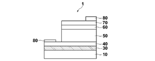
- FIG. 1 is a schematic cross-sectional view showing an embodiment of a photoelectric conversion element.
- the photoelectric conversion element 1 includes an anodic oxide film 20 formed by anodic oxidation, an alkali metal silicate layer 30, a molybdenum electrode 40, and holes / holes by light absorption.
- a photoelectric conversion semiconductor layer 50 that generates electron pairs, a buffer layer 60, a translucent conductive layer (transparent electrode) 70, and an upper electrode (grid electrode) 80 are sequentially stacked.
- 1 shows a photoelectric conversion element in which an anodized film 20 formed by anodization and an alkali metal silicate layer 30 are formed on a substrate 10, but as shown in FIG. An embodiment in which an alkali metal silicate layer 30 is formed on the substrate 10 may be used (in FIG. 2, components equivalent to those in FIG. 1 are given the same numbers). .
- a ceramic substrate such as non-alkali glass, quartz glass, or alumina
- a metal substrate such as stainless steel, titanium foil, or silicon
- a polymer substrate such as polyimide
- a metal substrate is particularly preferable.
- a material in which a metal oxide film generated on the surface of a metal substrate by anodic oxidation becomes an insulator can be used.
- a substrate containing one metal or an alloy of the above metals is preferred.
- a clad material in which one or both surfaces of aluminum, stainless steel, or steel plate are integrated with an aluminum plate is more preferable from the viewpoint of easy formation of anodization and high durability.
- an integrated clad material with both surfaces sandwiched between aluminum plates it is possible to suppress substrate warpage due to the difference in thermal expansion coefficient between aluminum and the oxide film (Al 2 O 3 ), and film peeling due to this. Therefore, it is more preferable.
- cleaning treatment / polishing smoothing treatment if necessary, for example, a degreasing step for removing the adhering rolling oil, a desmut treatment step for dissolving the smut on the surface of the aluminum plate, and roughening the surface of the aluminum plate It is preferable to use one subjected to a roughening treatment step.
- the anodic oxide film 20 formed by anodic oxidation is obtained by forming an insulating oxide film having a plurality of pores by anodic oxidation, thereby ensuring high insulation.
- Anodization can be performed by immersing the substrate 10 as an anode in an electrolyte together with a cathode, and applying a voltage between the anode and the cathode. Carbon, aluminum, or the like is used as the cathode.
- the anodizing conditions are not particularly limited depending on the type of electrolyte used.
- the conditions are, for example, an electrolyte concentration of 0.1 to 2 mol / L, a liquid temperature of 5 to 80 ° C., a current density of 0.005 to 0.60 A / cm 2 , a voltage of 1 to 200 V, and an electrolysis time of 3 to 500 minutes. Is appropriate.
- the electrolyte is not particularly limited, and an acidic electrolytic solution containing one or more acids such as sulfuric acid, phosphoric acid, chromic acid, oxalic acid, malonic acid, sulfamic acid, benzenesulfonic acid, and amidosulfonic acid is preferable. Used.
- an electrolyte concentration of 0.2 to 1 mol / L, a liquid temperature of 10 to 80 ° C., a current density of 0.05 to 0.30 A / cm 2 , and a voltage of 30 to 150 V are preferable.
- the anodic oxide film is preferably composed of a barrier layer portion and a porous layer portion, and the porous layer portion has a compressive strain at room temperature.
- the barrier layer has compressive stress and the porous layer has tensile stress, it is known that the whole anodic oxide film becomes tensile stress in a thick film of several ⁇ m or more.
- a porous layer having a compressive stress can be produced.
- the entire anodic oxide film can be subjected to compressive stress, no cracking occurs due to the difference in thermal expansion during film formation, and long-term reliability near room temperature is excellent. Insulating film can be obtained.
- the magnitude of the compressive strain is preferably 0.01% or more, more preferably 0.05% or more, and particularly preferably 0.10% or more. Moreover, it is preferable that it is 0.25% or less.
- the compressive strain is less than 0.01%, although it is compressive strain, it is insufficient and the effect of crack resistance cannot be obtained. Therefore, when the final product is subjected to bending strain, undergoes a temperature cycle over a long period of time, or receives impact or stress from the outside, cracks occur in the anodized film formed as an insulating layer, resulting in insulating properties. Leading to a decline.
- the compressive strain is preferably 0.25% or less.
- the Young's modulus of the anodic oxide film is known to be about 50 to 150 GPa. Therefore, the magnitude of the compressive stress is preferably about 5 to 300 MPa.
- the heat treatment may be performed after the anodizing treatment.
- compressive stress is applied to the anodized film, and crack resistance is increased. Therefore, heat resistance and insulation reliability are improved, and the metal substrate with an insulating layer can be more suitably used.
- the heat treatment temperature is preferably 150 ° C. or higher. When the above clad material is used, heat treatment at 300 ° C. or higher is preferable. By performing the heat treatment in advance, the amount of water contained in the porous anodic oxide film can be reduced, and the insulation can be improved.
- An anodized film is an oxide film formed in an aqueous solution, and it is described in, for example, “Chemistry Letters Vol. 34, No. 9, (2005) p1286” that moisture is retained inside a solid.
- aqueous solution As known. From the solid-state NMR measurement of the anodic oxide film as in this document, it was found that the amount of water (OH group) inside the solid of the anodic oxide film decreased when heat-treated at 100 ° C. or higher, particularly at 200 ° C. or higher is there. Therefore, it is presumed that the combined state of Al—O and Al—OH changes due to heating and stress relaxation (annealing effect) occurs.
- the anodic oxide film preferably has a thickness of 3 to 50 ⁇ m.
- a film thickness of 3 ⁇ m or more it is possible to achieve both insulation, heat resistance during film formation by having compressive stress at room temperature, and long-term reliability.
- the film thickness is preferably 5 ⁇ m or more and 30 ⁇ m or less, and particularly preferably 5 ⁇ m or more and 20 ⁇ m or less.
- the film thickness is extremely thin, there is a possibility that damage due to mechanical impact during handling and electrical insulation cannot be prevented. In addition, the insulation and heat resistance are drastically reduced, and the deterioration with time increases. This is because the influence of the unevenness on the surface of the anodized film becomes relatively large due to the thin film thickness, the crack becomes the starting point of cracks, and the anodization derived from metal impurities contained in aluminum. The effect of metal precipitates, intermetallic compounds, metal oxides, and voids in the film is relatively large, resulting in a decrease in insulation, and breakage when the anodized film is subjected to external impact or stress. This is because cracks are likely to occur. As a result, when the anodic oxide film is less than 3 ⁇ m, the insulating property is lowered, so that it is not suitable for use as a flexible heat-resistant substrate or roll-to-roll production.
- the cause of the decrease in bending resistance is that when the anodized film is bent, the tensile stress at the interface between the surface and the aluminum differs, so the stress distribution in the cross-sectional direction increases and local stress concentration occurs. This is presumed to be easier.
- the cause of the decrease in thermal strain resistance is that when a tensile stress is applied to the anodized film due to the thermal expansion of the base material, a greater stress is applied to the interface with aluminum, and the stress distribution in the cross-sectional direction increases, resulting in local stress.
- the film thickness of the molybdenum electrode 40 is not limited and is preferably about 200 to 1000 nm.
- the photoelectric conversion semiconductor layer 50 is a compound semiconductor-based photoelectric conversion semiconductor layer, and is not particularly limited as a main component (the main component means a component of 20% by mass or more), and high photoelectric conversion efficiency is obtained.
- the main component means a component of 20% by mass or more
- a compound semiconductor, a compound semiconductor having a chalcopyrite structure, or a compound semiconductor having a defect stannite structure can be preferably used.
- I-III-VI Group 2 compounds CuInSe 2 , CuGaSe 2 , Cu (In, Ga) Se 2 , CuInS 2 , CuGaSe 2 , Cu (In, Ga) (S, Se) 2, etc.
- I-III 3 -VI 5 group compounds Culn 3 Se 5 , CuGa 3 Se 5 , Cu (ln, Ga) 3 Se 5 and the like.
- I-III-VI Group 2 compounds CuInSe 2 , CuGaSe 2 , Cu (In, Ga) Se 2 , CuInS 2 , CuGaSe 2 , Cu (In, Ga) (S Se) 2, etc.
- I-III 3 -VI 5 group compounds CuIn 3 Se 5 , CuGa 3 Se 5 , Cu (In, Ga) 3 Se 5 and the like can be preferably mentioned.
- the method for forming the photoelectric conversion semiconductor layer is not particularly limited.
- a CI (G) S-based photoelectric conversion semiconductor layer containing Cu, In, (Ga), and S can be formed using a method such as a selenization method or a multi-source evaporation method.
- the film thickness of the photoelectric conversion semiconductor layer 50 is not particularly limited, and is preferably 1.0 to 3.0 ⁇ m, particularly preferably 1.5 to 2.0 ⁇ m.
- the buffer layer 60 is not particularly limited, but CdS, ZnS, Zn (S, O) and / or Zn (S, O, OH), SnS, Sn (S, O) and / or Sn (S, O, OH).
- the thickness of the buffer layer 40 is preferably 10 nm to 2 ⁇ m, and more preferably 15 to 200 nm.
- the translucent conductive layer (transparent electrode) 70 is a layer that captures light and functions as an electrode that is paired with the lower electrode 40 and through which the current generated in the photoelectric conversion layer 50 flows.
- the composition of the translucent conductive layer 70 is not particularly limited, and n-ZnO such as ZnO: Al is preferable.
- the film thickness of the translucent conductive layer 70 is not particularly limited, and is preferably 50 nm to 2 ⁇ m.
- the upper electrode (grid electrode) 80 is not particularly limited, and examples thereof include Al.
- the thickness of the upper electrode 80 is not particularly limited and is preferably 0.1 to 3 ⁇ m.
- the photoelectric conversion element of the present invention is a compound semiconductor having at least one chalcopyrite structure in which the main component of the photoelectric conversion semiconductor layer is composed of an Ib group element, an IIIb group element, and a VIb group element.
- the photoelectric conversion semiconductor layer contains lithium ions or potassium ions and sodium ions. Lithium ions and potassium ions may contain both.
- Each content of lithium ion, potassium ion and sodium ion contained in the photoelectric conversion semiconductor layer is preferably 1 ⁇ 10 15 atms / cm 3 or more. More preferably, the content of sodium ions is 1 ⁇ 10 18 atms / cm 3 ⁇ 1 ⁇ 10 20 atms / cm 3, more preferably 2 ⁇ 10 18 atms / cm 3 ⁇ 1 ⁇ 10 20 atms / cm 3, further Is preferably 5 ⁇ 10 18 atoms / cm 3 to 1 ⁇ 10 20 atoms / cm 3 .
- the lithium ion or potassium ion content is 1 ⁇ 10 15 atms / cm 3 to 5 ⁇ 10 19 atms / cm 3 , more preferably 1 ⁇ 10 16 atms / cm 3 to 5 ⁇ 10 19 atms / cm 3 , 1 ⁇ 10 17 atoms / cm 3 to 5 ⁇ 10 19 atoms / cm 3 are preferable.
- Lithium ions or potassium ions and sodium ions contained in the photoelectric conversion semiconductor layer may be co-evaporated at the time of film formation of the photoelectric conversion semiconductor layer, or fluoride such as NaF, LiF, KF, etc. on the Mo electrode in advance. It may be evaporated.
- a photoelectric conversion semiconductor layer is formed on a Mo film containing Na, Li, or K, or a compound containing Na, Li, or K is deposited and post-annealed after the photoelectric conversion semiconductor layer is formed. Good.
- the photoelectric conversion element substrate with a molybdenum electrode according to the first aspect and the photoelectric conversion element substrate with a molybdenum electrode according to the second aspect may be used to transmit and diffuse the molybdenum electrode 40 from the alkali supply layer 30.
- the photoelectric conversion element substrate of the present invention can be preferably used for solar cells and the like. If necessary, a cover glass, a protective film, or the like can be attached to the photoelectric conversion element 1 to form a solar cell.
- a cover glass, a protective film, or the like can be attached to the photoelectric conversion element 1 to form a solar cell.
- the substrate for photoelectric conversion element of the present invention will be described in more detail with reference to examples.
- Lithium supply source (manufactured by Nissan Chemical, trade names: lithium silicate 45, lithium silicate 75, lithium hydroxide), potassium supply source (manufactured by Fuji Chemical, trade names: 1K potassium silicate, 2K potassium silicate), sodium supply source ( Showa Chemical Co., Ltd., trade name: No. 1 sodium silicate, No. 3 sodium silicate, and Toso Sangyo, trade name: No. 4 sodium silicate, high-mol sodium silicate, sodium hydroxide) and water are shown in Table 1.
- boron or sodium tetraborate as a boron supply source and phosphoric acid as a phosphoric acid source were added at a mass ratio shown in Table 2 to prepare a coating solution.
- the coating solution was dropped on the substrate, and an alkali metal silicate layer was formed by spin coating. Thereafter, the substrate was heat-treated at 450 ° C. for 30 minutes. After the heat treatment, Mo was formed to a thickness of 800 nm on the substrate by DC sputtering.
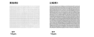
- Example 9 The amount of impurities on the Mo surface on the alkali metal silicate layer formed above was observed using an optical microscope to observe the amount of foreign matter.
- the micrographs of Example 9 and Comparative Example 1 are shown in FIG. In Example 9, no foreign matter was observed, but in Comparative Example 1, 10,000 or more foreign matters were observed per 1 mm square. Other examples and comparative examples were similarly observed with a microscope, and evaluated according to the following criteria according to the number of foreign matters per 1 mm square, and are shown in Tables 1 to 3.
- AA no foreign matter was observed
- A 1 to 10 foreign matters
- B 10 to less than 100 foreign matters
- C 10000 foreign matters
- a CIGS solar cell was formed on the Mo electrode.
- granular raw materials of high-purity copper and indium (purity 99.9999%), high-purity Ga (purity 99.999%), and high-purity Se (purity 99.999%) were used as the evaporation source.
- a chromel-alumel thermocouple was used as a substrate temperature monitor. After the main vacuum chamber is evacuated to 10 ⁇ 6 Torr (1.3 ⁇ 10 ⁇ 3 Pa), the deposition rate from each evaporation source is controlled, and the film thickness is about 530 ° C. under the film forming conditions. A 1.8 ⁇ m CIGS thin film was formed.
- a CdS thin film of about 90 nm was deposited as a buffer layer by a solution growth method, and a ZnO: A1 film of a transparent conductive film was formed thereon with a thickness of 0.6 ⁇ m by a DC sputtering method.
- an Al grid electrode was formed as an upper electrode by a vapor deposition method to produce a solar battery cell.
- AM Air Mass
- the photoelectric conversion efficiency was measured under the above conditions, and the maximum value among them was defined as the conversion efficiency of the photoelectric conversion element of each example and comparative example.
- the coefficient of variation (a value obtained by dividing the standard deviation of 8 cells by the average value) was evaluated as a variation in cell efficiency.
- the sodium concentration of the photoelectric converting layer was measured. This sodium concentration was measured using SIMS (secondary ion mass spectrometer). Primary ion species for measurement and Cs +, the acceleration voltage was set to 5.0 kV. Although the sodium concentration in the photoelectric conversion layer (CIGS layer) has a distribution in the thickness direction, it was integrated to derive an average value, and this average value was used for evaluation of the sodium concentration.
- Tables 1, 2 and 3 show the results of measurement of Mo film suitability, sodium concentration, and power generation efficiency together with the formulation of the coating solution.
- the mass ratio of the sodium source, lithium source and potassium source used in the examples and comparative examples Tables 4, 5 and 6 show.
- the molar ratios in Tables 1, 2 and 3 are converted from this mass ratio to molar ratio (so that sodium hydroxide and lithium hydroxide are solid).
- the sum of the molar ratio in Table 1 is a value calculated before rounding off the three decimal places of the molar ratio of lithium or potassium to silicon and the molar ratio of sodium to silicon.
- Examples 1 to 10 in which an alkali metal silicate layer containing lithium silicate or potassium silicate and sodium silicate was provided are alkali metal silicate layers made only of sodium silicate.
- the power generation efficiency was nearly double. In any of these cases, the sodium concentration is almost the same level, and it is considered that the sodium is sufficiently diffused into CIGS.
- Mo in Comparative Examples 5 to 8 has a high impurity peak ratio, which is attributed to this. It is thought that the power generation efficiency was low.
- Comparative Examples 1 and 2 which are alkali metal silicate layers made only of lithium silicate
- Comparative Examples 3 and 4 which are alkali metal silicate layers made only of potassium silicate
- the film forming suitability of Mo was good.
- the power generation efficiency was about 30% lower than that of the example on average. Since sodium is not present in the alkali metal silicate layer, it is considered that sodium was not diffused into CIGS and the efficiency was not improved. This shows that the power generation efficiency can be greatly increased by using lithium silicate or potassium silicate in combination with sodium silicate.
- Example 11 uses sodium hydroxide as a sodium supply source in place of sodium silicate and uses lithium silicate in combination.
- lithium hydroxide was used as a lithium supply source instead of lithium silicate, and sodium silicate was used in combination. Even in this case, the obtained alkali metal silicate is a mixture of sodium silicate and lithium silicate according to the present invention.
- film forming suitability and power generation efficiency were slightly low. This is presumably because the sum of the molar ratio of lithium to silicon and the molar ratio of sodium to silicon is greater than one.
- Example 13 was slightly inferior in power generation efficiency. This is considered because the molar ratio of lithium to silicon is larger than 1.
- FIG. 2 is an electron micrograph of CIGS crystals of Example 4 and Comparative Examples 1 and 5.
- Example 4 which is the substrate for photoelectric conversion elements of the present invention
- the grain size of the CIGS crystal is larger than that of Comparative Example 1, and the effect of adding an alkali is confirmed. It was.
- Comparative Example 5 also has a large particle size and an alkali addition effect, but the conversion efficiency is low because the suitability of Mo film formation is low and impurities are formed at the Mo / CIGS interface.
- the addition amount of the sodium source, the lithium source, and the potassium source was changed. From these examples, the molar ratio of lithium or potassium to silicon is in the range of 1 or less, and the sum of the molar ratio of lithium to silicon and the molar ratio of sodium to silicon is also 1 or less.
- the alkali metal silicate layer further contains boron or phosphorus. At first glance, it seems that there is no significant difference in power generation efficiency as compared with Examples not containing boron or phosphorus. As can be seen, since the coefficient of variation is small, all of the fabricated cells have high power generation efficiency, and it can be seen that the power generation efficiency of the entire fabricated cell is increased.
- a substrate As a substrate, a 3 cm square glass substrate, a SUS430 substrate (thickness: 100 ⁇ m), and an anodized aluminum substrate were prepared.
- the anodized aluminum substrate was produced by the following method. Each of a clad material made of 30 ⁇ m thick aluminum and 50 ⁇ m thick SUS430 is anodized under a constant voltage condition of 40 V using an oxalic acid electrolytic solution to produce a substrate on which 10 ⁇ m anodized aluminum is formed. did.
- the mixture was mixed to prepare a coating solution.
- the coating solution was dropped on the substrate, and an alkali metal silicate layer was formed by spin coating. Thereafter, the substrate was heat-treated at 450 ° C. for 30 minutes. After the heat treatment, Mo was formed to a thickness of 800 nm on the substrate by DC sputtering. In Comparative Example 3, the coating solution was solidified and could not be applied.
- Example 9 The amount of impurities on the Mo surface on the alkali metal silicate layer formed above was observed using an optical microscope to observe the amount of foreign matter.
- the micrographs of Example 9 and Comparative Example 1 are shown in FIG.
- Example 9 no foreign matter was observed, but in Comparative Example 1, 10,000 or more foreign matters were observed per 1 mm square.
- Other examples and comparative examples were similarly observed with a microscope, and evaluated according to the following criteria according to the number of foreign matters per 1 mm square, and are shown in Tables 1 and 2.
- AA no foreign matter was observed
- A 1 to 10 foreign matters
- B 10 to less than 100 foreign matters
- C 10000 foreign matters
- a CIGS solar cell was formed on the Mo electrode.
- granular raw materials of high-purity copper and indium (purity 99.9999%), high-purity Ga (purity 99.999%), and high-purity Se (purity 99.999%) were used as the evaporation source.
- a chromel-alumel thermocouple was used as a substrate temperature monitor. After the main vacuum chamber is evacuated to 10 ⁇ 6 Torr (1.3 ⁇ 10 ⁇ 3 Pa), the deposition rate from each evaporation source is controlled, and the film thickness is about 530 ° C. under the film forming conditions. A 1.8 ⁇ m CIGS thin film was formed.
- a CdS thin film of about 90 nm was deposited as a buffer layer by a solution growth method, and a ZnO: A1 film of a transparent conductive film was formed thereon with a thickness of 0.6 ⁇ m by a DC sputtering method.
- an Al grid electrode was formed as an upper electrode by a vapor deposition method to produce a solar battery cell.
- Eight samples were produced for each of the solar cells of Examples and Comparative Examples.
- the photoelectric conversion efficiency was measured under the above conditions, and the highest value and the coefficient of variation (the value obtained by dividing the standard deviation of 8 cells by the average value) in each example and comparative example solar cell. was evaluated as the conversion efficiency and variation.
- Tables 7 and 8 show the measurement results of the number of foreign matters and the power generation efficiency as Mo surface property evaluation together with the formulation of the coating solution.
- the molar ratios in Tables 7 and 8 are converted from the mass ratio to the molar ratio.
- Examples 10 to 16 the surface properties of Mo were further improved compared to Examples 1 to 5, and the power generation efficiency was high, and the variation was further reduced. This shows that the power generation efficiency can be further increased by using lithium silicate or potassium silicate in combination with sodium silicate.
- Examples 6 to 9 were obtained by reducing the molar ratio of boron or phosphorus in Example 4, and Examples 17 to 20 were obtained by reducing the molar ratio of boron or phosphorus in Example 11 or 13. From the comparison, it can be seen that the molar ratio of silicon to 0.002 or more is more preferable in order to reduce foreign substances.
Landscapes
- Chemical & Material Sciences (AREA)
- Engineering & Computer Science (AREA)
- Chemical Kinetics & Catalysis (AREA)
- Materials Engineering (AREA)
- Metallurgy (AREA)
- Organic Chemistry (AREA)
- Electrochemistry (AREA)
- Mechanical Engineering (AREA)
- General Chemical & Material Sciences (AREA)
- Inorganic Chemistry (AREA)
- Photovoltaic Devices (AREA)
Abstract
L'invention vise à procurer un substrat pour un élément de conversion électrique dans lequel il est possible de diffuser efficacement des ions de métaux alcalins dans une couche semi-conductrice de conversion photoélectrique, et dans lequel le rendement de conversion photoélectrique de l'élément de conversion photoélectrique est accru. A cet effet, l'invention porte sur un substrat pour un élément de conversion photoélectrique, lequel substrat est réalisé de façon à comprendre une couche de silicate de métal alcalin (30), qui comprend du silicate de sodium et du silicate de lithium ou du silicate de potassium sur un substrat (10), ou est, en variante, réalisé de façon à comprendre une couche de silicate de métal alcalin (30) (ne contenant pas de métaux alcalino-terreux), qui comprend du silicium, un métal alcalin et au moins un type parmi des éléments du groupe 13 autres que l'aluminium et des éléments du groupe 15 autres que l'azote, et qui est formée sur un substrat (10) à l'aide d'un procédé en phase liquide.
Applications Claiming Priority (8)
| Application Number | Priority Date | Filing Date | Title |
|---|---|---|---|
| JP2011-083336 | 2011-04-05 | ||
| JP2011083336 | 2011-04-05 | ||
| JP2011-212194 | 2011-09-28 | ||
| JP2011212197 | 2011-09-28 | ||
| JP2011-212195 | 2011-09-28 | ||
| JP2011212194 | 2011-09-28 | ||
| JP2011212195A JP5000779B1 (ja) | 2011-04-05 | 2011-09-28 | モリブデン電極付光電変換素子用基板 |
| JP2011-212197 | 2011-09-28 |
Publications (1)
| Publication Number | Publication Date |
|---|---|
| WO2012137497A1 true WO2012137497A1 (fr) | 2012-10-11 |
Family
ID=46968906
Family Applications (1)
| Application Number | Title | Priority Date | Filing Date |
|---|---|---|---|
| PCT/JP2012/002354 Ceased WO2012137497A1 (fr) | 2011-04-05 | 2012-04-04 | Substrat pour élément de conversion photoélectrique ayant une électrode en molybdène, élément de conversion photoélectrique et cellule solaire |
Country Status (2)
| Country | Link |
|---|---|
| TW (1) | TW201242038A (fr) |
| WO (1) | WO2012137497A1 (fr) |
Cited By (2)
| Publication number | Priority date | Publication date | Assignee | Title |
|---|---|---|---|---|
| EP2876694A1 (fr) * | 2013-11-20 | 2015-05-27 | Samsung SDI Co., Ltd. | Cellule solaire |
| CN113646460A (zh) * | 2019-03-29 | 2021-11-12 | 富士胶片株式会社 | 铝箔、铝箔的制造方法、集电体、锂离子电容器及锂离子电池 |
Families Citing this family (1)
| Publication number | Priority date | Publication date | Assignee | Title |
|---|---|---|---|---|
| KR102248704B1 (ko) | 2012-12-21 | 2021-05-06 | 프리솜 에이쥐 | 칼륨이 첨가되는 박막 광전자 소자의 제조 |
Citations (7)
| Publication number | Priority date | Publication date | Assignee | Title |
|---|---|---|---|---|
| JPS6119796A (ja) * | 1984-07-06 | 1986-01-28 | Fujikura Ltd | 陽極酸化皮膜の強化方法 |
| JPH08222750A (ja) * | 1994-12-01 | 1996-08-30 | Siemens Ag | 基板上に太陽電池を製造する方法及びカルコパイライト吸収層を有する太陽電池 |
| JPH1074966A (ja) * | 1996-08-29 | 1998-03-17 | Moririka:Kk | 薄膜太陽電池の製造方法 |
| JP2004047860A (ja) * | 2002-07-15 | 2004-02-12 | Matsushita Electric Ind Co Ltd | 薄膜太陽電池およびその製造方法 |
| JP2009267332A (ja) * | 2007-09-28 | 2009-11-12 | Fujifilm Corp | 太陽電池用基板および太陽電池 |
| JP2010239129A (ja) * | 2009-03-10 | 2010-10-21 | Fujifilm Corp | 光電変換素子及び太陽電池、光電変換素子の製造方法 |
| JP2010251694A (ja) * | 2009-03-26 | 2010-11-04 | Fujifilm Corp | 光電変換半導体層とその製造方法、光電変換素子、及び太陽電池 |
-
2012
- 2012-04-04 WO PCT/JP2012/002354 patent/WO2012137497A1/fr not_active Ceased
- 2012-04-05 TW TW101112086A patent/TW201242038A/zh unknown
Patent Citations (7)
| Publication number | Priority date | Publication date | Assignee | Title |
|---|---|---|---|---|
| JPS6119796A (ja) * | 1984-07-06 | 1986-01-28 | Fujikura Ltd | 陽極酸化皮膜の強化方法 |
| JPH08222750A (ja) * | 1994-12-01 | 1996-08-30 | Siemens Ag | 基板上に太陽電池を製造する方法及びカルコパイライト吸収層を有する太陽電池 |
| JPH1074966A (ja) * | 1996-08-29 | 1998-03-17 | Moririka:Kk | 薄膜太陽電池の製造方法 |
| JP2004047860A (ja) * | 2002-07-15 | 2004-02-12 | Matsushita Electric Ind Co Ltd | 薄膜太陽電池およびその製造方法 |
| JP2009267332A (ja) * | 2007-09-28 | 2009-11-12 | Fujifilm Corp | 太陽電池用基板および太陽電池 |
| JP2010239129A (ja) * | 2009-03-10 | 2010-10-21 | Fujifilm Corp | 光電変換素子及び太陽電池、光電変換素子の製造方法 |
| JP2010251694A (ja) * | 2009-03-26 | 2010-11-04 | Fujifilm Corp | 光電変換半導体層とその製造方法、光電変換素子、及び太陽電池 |
Cited By (3)
| Publication number | Priority date | Publication date | Assignee | Title |
|---|---|---|---|---|
| EP2876694A1 (fr) * | 2013-11-20 | 2015-05-27 | Samsung SDI Co., Ltd. | Cellule solaire |
| CN113646460A (zh) * | 2019-03-29 | 2021-11-12 | 富士胶片株式会社 | 铝箔、铝箔的制造方法、集电体、锂离子电容器及锂离子电池 |
| CN113646460B (zh) * | 2019-03-29 | 2023-08-15 | 富士胶片株式会社 | 铝箔、铝箔的制造方法、集电体、锂离子电容器及锂离子电池 |
Also Published As
| Publication number | Publication date |
|---|---|
| TW201242038A (en) | 2012-10-16 |
Similar Documents
| Publication | Publication Date | Title |
|---|---|---|
| JP5727402B2 (ja) | 絶縁層付金属基板およびその製造方法並びに半導体装置 | |
| JP5480782B2 (ja) | 太陽電池および太陽電池の製造方法 | |
| JP4629151B2 (ja) | 光電変換素子及び太陽電池、光電変換素子の製造方法 | |
| JP4700130B1 (ja) | 絶縁性金属基板および半導体装置 | |
| JP2013084921A (ja) | 光電変換素子および太陽電池 | |
| US20110186102A1 (en) | Photoelectric conversion element, thin-film solar cell, and photoelectric conversion element manufacturing method | |
| CN102754218A (zh) | 具有绝缘层的金属基板及其制备方法、半导体器件及其制备方法、太阳能电池及其制备方法、电子电路及其制备方法以及发光元件及其制备方法 | |
| JP5000779B1 (ja) | モリブデン電極付光電変換素子用基板 | |
| JPWO2003069684A1 (ja) | 光吸収層の作製方法 | |
| JP2011176266A (ja) | Se化合物半導体用基板、Se化合物半導体用基板の製造方法および薄膜太陽電池 | |
| JP2011176285A (ja) | 光電変換素子、薄膜太陽電池および光電変換素子の製造方法 | |
| CN103201846A (zh) | 光电转换元件 | |
| WO2012137497A1 (fr) | Substrat pour élément de conversion photoélectrique ayant une électrode en molybdène, élément de conversion photoélectrique et cellule solaire | |
| JP5634315B2 (ja) | 絶縁層付金属基板および光電変換素子 | |
| JP2011176288A (ja) | 光電変換素子、薄膜太陽電池および光電変換素子の製造方法 | |
| US20110186123A1 (en) | Substrate with insulation layer and thin-film solar cell | |
| JP2010232427A (ja) | 光電変換素子、その製造方法、それに用いられる陽極酸化基板及び太陽電池 | |
| TW201318180A (zh) | 光電轉換元件用基板及光電轉換元件 | |
| JP2014107510A (ja) | 化合物系薄膜太陽電池 | |
| JP2010258255A (ja) | 陽極酸化基板、それを用いた光電変換素子の製造方法、光電変換素子及び太陽電池 | |
| JP2013077706A (ja) | 光電変換素子およびその製造方法 | |
| JP2013044000A (ja) | 絶縁層付金属基板およびその製造方法、半導体装置およびその製造方法、太陽電池およびその製造方法、電子回路およびその製造方法、ならびに発光素子およびその製造方法 | |
| WO2010032803A1 (fr) | Substrat de cellule solaire et cellule solaire associee | |
| JP2011159685A (ja) | 太陽電池の製造方法 | |
| JP2014183197A (ja) | 半導体素子用基板、光電変換素子および太陽電池 |
Legal Events
| Date | Code | Title | Description |
|---|---|---|---|
| 121 | Ep: the epo has been informed by wipo that ep was designated in this application |
Ref document number: 12768060 Country of ref document: EP Kind code of ref document: A1 |
|
| NENP | Non-entry into the national phase |
Ref country code: DE |
|
| 122 | Ep: pct application non-entry in european phase |
Ref document number: 12768060 Country of ref document: EP Kind code of ref document: A1 |