WO2012137555A1 - Commutateur optique de guide d'ondes - Google Patents
Commutateur optique de guide d'ondes Download PDFInfo
- Publication number
- WO2012137555A1 WO2012137555A1 PCT/JP2012/054373 JP2012054373W WO2012137555A1 WO 2012137555 A1 WO2012137555 A1 WO 2012137555A1 JP 2012054373 W JP2012054373 W JP 2012054373W WO 2012137555 A1 WO2012137555 A1 WO 2012137555A1
- Authority
- WO
- WIPO (PCT)
- Prior art keywords
- switch
- input
- output
- waveguide type
- outputs
- Prior art date
- Legal status (The legal status is an assumption and is not a legal conclusion. Google has not performed a legal analysis and makes no representation as to the accuracy of the status listed.)
- Ceased
Links
Images


Classifications
-
- H—ELECTRICITY
- H04—ELECTRIC COMMUNICATION TECHNIQUE
- H04Q—SELECTING
- H04Q11/00—Selecting arrangements for multiplex systems
- H04Q11/0001—Selecting arrangements for multiplex systems using optical switching
- H04Q11/0005—Switch and router aspects
-
- H—ELECTRICITY
- H01—ELECTRIC ELEMENTS
- H01P—WAVEGUIDES; RESONATORS, LINES, OR OTHER DEVICES OF THE WAVEGUIDE TYPE
- H01P1/00—Auxiliary devices
- H01P1/10—Auxiliary devices for switching or interrupting
- H01P1/12—Auxiliary devices for switching or interrupting by mechanical chopper
- H01P1/122—Waveguide switches
-
- H—ELECTRICITY
- H04—ELECTRIC COMMUNICATION TECHNIQUE
- H04Q—SELECTING
- H04Q11/00—Selecting arrangements for multiplex systems
- H04Q11/0001—Selecting arrangements for multiplex systems using optical switching
- H04Q11/0005—Switch and router aspects
- H04Q2011/0007—Construction
- H04Q2011/0024—Construction using space switching
-
- H—ELECTRICITY
- H04—ELECTRIC COMMUNICATION TECHNIQUE
- H04Q—SELECTING
- H04Q11/00—Selecting arrangements for multiplex systems
- H04Q11/0001—Selecting arrangements for multiplex systems using optical switching
- H04Q11/0005—Switch and router aspects
- H04Q2011/0052—Interconnection of switches
- H04Q2011/0058—Crossbar; Matrix
Definitions
- the present invention relates to a waveguide type optical switch capable of providing not only a cross-connect function for switching a one-to-one connection relationship but also a distribution function for branching an input signal and outputting it to a plurality of ports.
- An optical cross-connect with N inputs and N outputs uses a MEMS (Micro-Electro-Mechanical-Systems; MEMS) element (see Patent Document 1), a waveguide-type optical switch (matrix switch) (see Patent Document 2) ) Etc.
- MEMS Micro-Electro-Mechanical-Systems
- the waveguide type optical switch includes a switch element and a fiber array for input and output connected to the switch element.
- a MEMS device in which an optical switch is made small by a semiconductor technology is a method in which a small mirror is produced on a substrate by a semiconductor manufacturing technology, the mirror is raised by static electricity, and an optical path is switched.
- a conventional waveguide type N ⁇ N matrix switch uses N 2 2 ⁇ 2 crossbar switches as element switches.
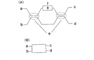
- the element switch is configured by a 2 ⁇ 2 waveguide type Mach-Zehnder interferometer as illustrated in FIG. 12 (see Non-Patent Document 1).
- FIG. 12A is a diagram illustrating a two-input (a, b), two-output (c, d) waveguide type Mach-Zehnder interferometer as an element switch, and (B) is a simplified representation of the element switch. Is shown.
- the illustrated waveguide type Mach-Zehnder interferometer is composed of two 3 dB splitters (e) and a phase shifter (f), and can change the branching ratio by the phase shift amount of the phase shifter (f).
- Output (2 ⁇ 2) variable branch The light incident from the input end a or b is divided into two light waves by the left 3dB splitter (e), propagates through the upper and lower optical paths of the same length, and then combined by the right 3dB splitter (e).
- the way of output from the terminals c and d varies depending on the phase change ⁇ given to the phase shifter (f).
- the waveguide type Mach-Zehnder interferometer is a 2 ⁇ 2 variable branch whose branching ratio can be continuously changed by the phase shifter, but the conventional waveguide type N ⁇ N matrix switch is a waveguide type Mach.
- the Zender interferometer was used only as a crossbar switch, and no other branching ratio state was used.
- the node device has both a cross-connect (switching of one-to-one connection relationship) function and a function of distributing one input signal to a plurality of output ports.
- the conventional single (1 ⁇ N) branch element has the function of distributing one input signal to a plurality of output ports, but the number of branches and the output port of the branch destination Is fixed, and the output port of the branched signal cannot be set arbitrarily, so that it cannot cope with services such as video distribution.
- the present invention solves such problems, and in a waveguide type optical switch (matrix switch) with N inputs and N outputs (N ⁇ N), a cross-connect (switching of one-to-one connection relationship) function and one input It is intended to provide a function for distributing signals to a plurality of output ports.
- Another object of the present invention is to create all possible one-to-one connections, distribution, and a mixed state of both by appropriately determining the role of the variable branch of each of the N 2 element switches.
- N 2 element switches having 2 inputs and 2 outputs are arranged on a lattice of a matrix of N rows and N columns, where N is an integer.
- Each of the N 2 element switches has a variable branch configuration in which the branch ratio of the two outputs is made variable, and the N 2 element switches include the element switch and the bar state set to the cross state.
- the element switch set to 1 the element switch set to be distributed to two outputs at a predetermined branching ratio is included.
- This element switch is a two-input two-output waveguide type Mach-Zehnder interferometer which is composed of two 3 dB ⁇ splitters and a phase shifter and whose branching ratio can be changed by the phase shift amount of the phase shifter.
- a single waveguide type optical switch can be used as an N ⁇ N cross-connect or a 1 ⁇ M branch (M ⁇ N) (M and N are integers), as well as a cross-connect function and a branch function. Mixing operation is possible. Further, in the 1 ⁇ M branch, the number of branches and the branch destination output port can be arbitrarily set.
- each of the element switches constituting a general N ⁇ N waveguide type optical switch a cross state, a bar state, a branch of a predetermined distribution ratio, and respective arrangements are appropriately selected. By correcting, it is possible to create a desired one-to-one connection, distribution to multiple ports, or a mixture of both.
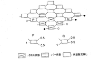
- FIG. 1 It is a figure which illustrates the waveguide type optical switch (matrix switch) structure comprised based on this invention.
- A) is a figure explaining operation
- (B) is a figure which shows a cross connection and (C) respectively shows a bar connection. It is a figure explaining the setting of each variable branch in the case of performing 1 ⁇ 4 distribution of one system ( ⁇ ).
- ⁇ 1x3 distribution of 1 system ((circle)) and 1x1 connection of 1 system ((circle)) are performed.
- 1x2 distribution of 2 systems ((circle) and ⁇ ) is performed.
- FIG. 1 It is a figure which illustrates the case where 1x2 distribution of 1 system ((circle)) and 1x1 connection of 2 systems ( ⁇ , ⁇ ) are performed. It is a figure which illustrates another waveguide type optical switch (matrix switch) structure different from FIG. 1 comprised based on this invention. It is a figure explaining the setting of each variable branch in the case of performing 1 ⁇ 4 distribution of one system ( ⁇ ). It is a figure which illustrates the case where 1x3 distribution of 1 system ((circle)) and 1x1 connection of 1 system ((circle)) are performed. It is a figure which illustrates the case where 1x2 distribution of 2 systems ((circle) and ⁇ ) is performed.
- FIG. 1 is a diagram illustrating a two-input (a, b), two-output (c, d) waveguide type Mach-Zehnder interferometer as an element switch, and (B) shows a simplified display of the element switch.
- a matrix switch called a Pyros type uses N 2 switch cells each having 2 inputs and 2 outputs in order to eliminate variations in loss due to the number of passing switch cells (element switches). They are arranged on a matrix of rows and N columns, and are configured by appropriately connecting the input and output of the switch cell so as not to cause loss path dependency.
- FIG. 1 is a diagram illustrating a waveguide type optical switch (matrix switch) configuration configured according to the present invention.
- the illustrated waveguide type optical switch is configured by arranging N 2 element switches (S 11 to S NN ) each having 2 inputs and 2 outputs on a matrix grid of N rows and N columns.
- Each element switch is a variable input with 2 inputs and 2 outputs (2 x 2), and each element switch can be operated in either a cross state, a bar state, or a predetermined branch ratio. It is possible to have a distribution function of branching a signal and outputting it to a plurality of ports.
- FIG. 2A is a diagram for explaining the operation of the element switch shown in FIG. 1, where FIG. 2B shows a cross connection and FIG. 2C shows a bar connection.
- the element switch is configured by a 2 ⁇ 2 waveguide type Mach-Zehnder interferometer as illustrated in FIG.
- the illustrated element switch can be operated as a cross connection or a bar connection by changing the phase shift amount ⁇ of the phase shifter, in addition to a predetermined branch ratio (for example, 1: 1, 1: 2 or 1: 3).
- phase shift amount ⁇ of the phase shifter can be changed by, for example, a thermo-optic effect, a carrier plasma effect, an electro-optic effect, or the like.
- FIG. 3 shows a variable branch setting for equally distributing one input signal to all four output ports. It is assumed that a signal is input from only one port and no signal is input to the remaining three ports.
- variable branches indicated as P, Q, and R in the figure are set so as to have the branching ratio shown in the lower part of the figure. As a result, one input signal is equally distributed to all four output ports.
- FIG. 4 is a diagram illustrating a case where 1 ⁇ 3 distribution of 1 system ( ⁇ ) and 1 ⁇ 1 connection of 1 system ( ⁇ ) are performed. This is a case where a signal input to one port is equally distributed to three output ports, and an input to another port is connected to the remaining one output port.
- the variable branches marked P and Q in the figure are set so as to have the branching ratio shown in the lower part of the figure.
- FIG. 5 is a diagram illustrating a case where 1 ⁇ 2 distribution of two systems ( ⁇ , ⁇ ) is performed. A case where signals input to two ports are equally distributed to two output ports is shown. The variable branches marked P and Q in the figure are set so as to have the branching ratio shown in the lower part of the figure.
- FIG. 6 is a diagram illustrating a case where 1 ⁇ 2 distribution of 1 system ( ⁇ ) and 1 ⁇ 1 connection of 2 systems ( ⁇ , ⁇ ) are performed.
- a case is shown in which a signal input to one port is equally distributed to two output ports, and signals input to the two ports are connected to different output ports, respectively.
- the variable branch marked P in the figure is set so as to have the branching ratio shown in the lower part of the figure.
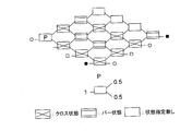
- FIG. 7 shows another standard matrix topology that is not Pyros but is different from FIG.
- the standard matrix topology itself shown in the figure has N 2 element switches (S 11 to S NN ) each having 2 inputs and 2 outputs arranged on a matrix grid of N rows and N columns. ,Constitute. Connection paths from the input side are element switches S 11 to S N1 , and connection paths to the output side are element switches S N1 to S NN .
- An arbitrary input side connection path has a cross point at one position between the arbitrary input side connection path and a path is set between both connection paths. For this path setting, the cross point element switch is switched from cross connection to bar connection.
- the present invention can be applied to a standard matrix topology known per se, which is conventionally configured by setting element switches to either a cross connection or a bar connection.
- all N 2 element switches (S 11 to S NN ) have two inputs and two outputs (2 ⁇ ) as described with reference to FIG. 2)
- the variable branch element switch is used.
- one or more element switches are operated at a predetermined branching ratio.
- FIGS. 8 to 11 show that the operation corresponding to FIGS. 3 to 6 is possible even with this standard matrix topology.
- FIG. 8 is a diagram for explaining the setting of each variable branch when 1 ⁇ 4 distribution of one system ( ⁇ ) is performed. This corresponds to the case of FIG.
- FIG. 9 is a diagram illustrating a case where 1 ⁇ 3 distribution of 1 system ( ⁇ ) and 1 ⁇ 1 connection of 1 system ( ⁇ ) are performed. This corresponds to the case of FIG.
- FIG. 10 is a diagram illustrating a case where 1 ⁇ 2 distribution of two systems ( ⁇ , ⁇ ) is performed. This corresponds to the case of FIG.
- FIG. 11 is a diagram illustrating a case where 1 ⁇ 2 distribution of 1 system ( ⁇ ) and 1 ⁇ 1 connection of 2 systems ( ⁇ , ⁇ ) are performed. This corresponds to the case of FIG.
- FIGS. 3 and 8 show 1 ⁇ 4 as 1 system
- FIGS. 4 and 9 show 1 ⁇ 3 and 1 ⁇ 1 as 1 system
- FIGS. 5 and 10 show 1 ⁇ 2 as 2 systems
- 6 and 11 show an example in which 1 ⁇ 2 includes 1 system and 1 ⁇ 1 includes 2 systems.
- Bars special branching ratios such as P, Q, and R above, creating the desired one-to-one connection, distribution to multiple ports, or a mixture of both by properly re-selecting each placement Can do.
- N ⁇ N matrix all possible one-to-one connections, distribution, and a mixture of both can be achieved by appropriately determining the role of the variable branch of each of the N 2 element switches. You can create a state.
Landscapes
- Engineering & Computer Science (AREA)
- Computer Networks & Wireless Communication (AREA)
- Optical Modulation, Optical Deflection, Nonlinear Optics, Optical Demodulation, Optical Logic Elements (AREA)
- Optical Integrated Circuits (AREA)
Abstract
L'invention porte sur un commutateur optique de guide d'ondes à N entrées et N sorties (N x N) (commutateur à matrice), lequel commutateur possède à la fois une fonction de connexion croisée (commutation en une relation de connexion un à un) et une fonction de distribution d'un signal d'entrée unique à de multiples ports de sortie. Dans la présente invention, un nombre N² d'éléments de commutation à 2 entrées et 2 sorties sont disposés sur la grille d'une matrice ayant N rangées et N colonnes. Chacun du nombre N² d'éléments de commutation a une configuration à divergence variable qui fait varier le rapport de divergence de deux sorties à faire sortir. De plus, le nombre N² d'éléments de commutation comprend, en plus d'un élément de commutation configuré avec un état croisé et d'un élément de commutation configuré avec un état barre, un élément de commutation configuré de façon à produire une distribution à deux sorties à un certain rapport de divergence.
Applications Claiming Priority (2)
| Application Number | Priority Date | Filing Date | Title |
|---|---|---|---|
| JP2011085323A JP2012220664A (ja) | 2011-04-07 | 2011-04-07 | 導波路型光スイッチ |
| JP2011-085323 | 2011-04-07 |
Publications (1)
| Publication Number | Publication Date |
|---|---|
| WO2012137555A1 true WO2012137555A1 (fr) | 2012-10-11 |
Family
ID=46968959
Family Applications (1)
| Application Number | Title | Priority Date | Filing Date |
|---|---|---|---|
| PCT/JP2012/054373 Ceased WO2012137555A1 (fr) | 2011-04-07 | 2012-02-23 | Commutateur optique de guide d'ondes |
Country Status (2)
| Country | Link |
|---|---|
| JP (1) | JP2012220664A (fr) |
| WO (1) | WO2012137555A1 (fr) |
Cited By (1)
| Publication number | Priority date | Publication date | Assignee | Title |
|---|---|---|---|---|
| JP2014086802A (ja) * | 2012-10-22 | 2014-05-12 | Oki Electric Ind Co Ltd | 多端末量子鍵配送システム |
Families Citing this family (2)
| Publication number | Priority date | Publication date | Assignee | Title |
|---|---|---|---|---|
| CN103973369B (zh) * | 2014-05-16 | 2016-03-23 | 电子科技大学 | 一种光开关矩阵的状态配置方法 |
| JP6950593B2 (ja) * | 2018-03-09 | 2021-10-13 | 日本電信電話株式会社 | 光入出力装置およびその作製方法 |
Citations (2)
| Publication number | Priority date | Publication date | Assignee | Title |
|---|---|---|---|---|
| JP2003005231A (ja) * | 2001-06-26 | 2003-01-08 | Nippon Telegr & Teleph Corp <Ntt> | 光マトリクススイッチ |
| WO2011043122A1 (fr) * | 2009-10-07 | 2011-04-14 | 日本電気株式会社 | Appareil de transmission de signal optique, appareil de réception de signal optique, appareil de communication optique de démultiplexage de longueur d'onde et système de trajet de longueur d'onde |
-
2011
- 2011-04-07 JP JP2011085323A patent/JP2012220664A/ja active Pending
-
2012
- 2012-02-23 WO PCT/JP2012/054373 patent/WO2012137555A1/fr not_active Ceased
Patent Citations (2)
| Publication number | Priority date | Publication date | Assignee | Title |
|---|---|---|---|---|
| JP2003005231A (ja) * | 2001-06-26 | 2003-01-08 | Nippon Telegr & Teleph Corp <Ntt> | 光マトリクススイッチ |
| WO2011043122A1 (fr) * | 2009-10-07 | 2011-04-14 | 日本電気株式会社 | Appareil de transmission de signal optique, appareil de réception de signal optique, appareil de communication optique de démultiplexage de longueur d'onde et système de trajet de longueur d'onde |
Non-Patent Citations (1)
| Title |
|---|
| MIZUTANI, K. ET AL.: "Demonstraion of Multi- Degree Color/Direction-Independent Waveguide- Based Transponder-Aggregator for Flexible Optical Path Networks", ECOC 2010, September 2010 (2010-09-01), pages 1 - 3, XP031789618 * |
Cited By (1)
| Publication number | Priority date | Publication date | Assignee | Title |
|---|---|---|---|---|
| JP2014086802A (ja) * | 2012-10-22 | 2014-05-12 | Oki Electric Ind Co Ltd | 多端末量子鍵配送システム |
Also Published As
| Publication number | Publication date |
|---|---|
| JP2012220664A (ja) | 2012-11-12 |
Similar Documents
| Publication | Publication Date | Title |
|---|---|---|
| Dupuis et al. | Design and Fabrication of Low-Insertion-Loss and Low-Crosstalk Broadband Mach–Zehnder Silicon Photonic Switches | |
| Dupuis et al. | Modeling and Characterization of a Nonblocking $4\times 4$ Mach–Zehnder Silicon Photonic Switch Fabric | |
| JP3842511B2 (ja) | 多重ポート・カプラを使用する光学的空間スイッチ | |
| US6292597B1 (en) | N×N non-blocking optical switch | |
| JP5222083B2 (ja) | 多方路光スイッチ | |
| JP5913139B2 (ja) | 導波路型光スイッチ | |
| US9794656B2 (en) | Modular photonic switch architecture | |
| US9784921B1 (en) | Switch matrix incorporating polarization controller | |
| EP3021595B1 (fr) | Répartiteur optique | |
| WO2012137555A1 (fr) | Commutateur optique de guide d'ondes | |
| Suzuki et al. | Low loss fully reconfigurable wavelength-selective optical 1/spl times/N switch based on transversal filter configuration using silica-based planar lightwave circuit | |
| Suzuki et al. | High-Speed Optical 1$\times $4 Switch Based on Generalized Mach–Zehnder Interferometer With Hybrid Configuration of Silica-Based PLC and Lithium Niobate Phase-Shifter Array | |
| JP6420715B2 (ja) | 光信号処理装置 | |
| Bahadori et al. | Loss and crosstalk of scalable MZI-based switch topologies in silicon photonic platform | |
| JP2004233619A (ja) | 光スイッチ及び光波長ルータ | |
| JP2016161604A (ja) | 光スイッチ装置 | |
| JP7189473B2 (ja) | 光信号処理装置 | |
| US20020044318A1 (en) | Add/drop apparatus using multiple wavelength michelson interferometer | |
| JP2006292872A (ja) | マトリクス光スイッチ | |
| US20020044714A1 (en) | Multiple wavelength Michelson interferometer switch | |
| Suzuki et al. | Ultra-compact Si-wire 8× 8 strictly-non-blocking PILOSS switch | |
| Kawashima et al. | Multi-port optical switch based on silicon photonics | |
| US11405702B2 (en) | Optical signal processing device and method for controlling same | |
| Moralis-Pegios et al. | A programmable Si-photonic node for SDN-enabled Bloom filter forwarding in disaggregated data centers | |
| Hoppe et al. | Improved Optical 1xN On-Chip-Switches Based on Generalized Mach-Zehnder Interferometers |
Legal Events
| Date | Code | Title | Description |
|---|---|---|---|
| 121 | Ep: the epo has been informed by wipo that ep was designated in this application |
Ref document number: 12767811 Country of ref document: EP Kind code of ref document: A1 |
|
| NENP | Non-entry into the national phase |
Ref country code: DE |
|
| 122 | Ep: pct application non-entry in european phase |
Ref document number: 12767811 Country of ref document: EP Kind code of ref document: A1 |