WO2012137586A1 - Appareil d'imagerie et procédé de production d'appareil d'imagerie - Google Patents
Appareil d'imagerie et procédé de production d'appareil d'imagerie Download PDFInfo
- Publication number
- WO2012137586A1 WO2012137586A1 PCT/JP2012/056912 JP2012056912W WO2012137586A1 WO 2012137586 A1 WO2012137586 A1 WO 2012137586A1 JP 2012056912 W JP2012056912 W JP 2012056912W WO 2012137586 A1 WO2012137586 A1 WO 2012137586A1
- Authority
- WO
- WIPO (PCT)
- Prior art keywords
- heat
- sensor substrate
- imaging device
- solid
- signal processing
- Prior art date
- Legal status (The legal status is an assumption and is not a legal conclusion. Google has not performed a legal analysis and makes no representation as to the accuracy of the status listed.)
- Ceased
Links
Images






Classifications
-
- G—PHYSICS
- G03—PHOTOGRAPHY; CINEMATOGRAPHY; ANALOGOUS TECHNIQUES USING WAVES OTHER THAN OPTICAL WAVES; ELECTROGRAPHY; HOLOGRAPHY
- G03B—APPARATUS OR ARRANGEMENTS FOR TAKING PHOTOGRAPHS OR FOR PROJECTING OR VIEWING THEM; APPARATUS OR ARRANGEMENTS EMPLOYING ANALOGOUS TECHNIQUES USING WAVES OTHER THAN OPTICAL WAVES; ACCESSORIES THEREFOR
- G03B30/00—Camera modules comprising integrated lens units and imaging units, specially adapted for being embedded in other devices, e.g. mobile phones or vehicles
-
- G—PHYSICS
- G03—PHOTOGRAPHY; CINEMATOGRAPHY; ANALOGOUS TECHNIQUES USING WAVES OTHER THAN OPTICAL WAVES; ELECTROGRAPHY; HOLOGRAPHY
- G03B—APPARATUS OR ARRANGEMENTS FOR TAKING PHOTOGRAPHS OR FOR PROJECTING OR VIEWING THEM; APPARATUS OR ARRANGEMENTS EMPLOYING ANALOGOUS TECHNIQUES USING WAVES OTHER THAN OPTICAL WAVES; ACCESSORIES THEREFOR
- G03B33/00—Colour photography, other than mere exposure or projection of a colour film
- G03B33/10—Simultaneous recording or projection
- G03B33/12—Simultaneous recording or projection using beam-splitting or beam-combining systems, e.g. dichroic mirrors
-
- H—ELECTRICITY
- H04—ELECTRIC COMMUNICATION TECHNIQUE
- H04N—PICTORIAL COMMUNICATION, e.g. TELEVISION
- H04N23/00—Cameras or camera modules comprising electronic image sensors; Control thereof
- H04N23/50—Constructional details
- H04N23/51—Housings
-
- G—PHYSICS
- G03—PHOTOGRAPHY; CINEMATOGRAPHY; ANALOGOUS TECHNIQUES USING WAVES OTHER THAN OPTICAL WAVES; ELECTROGRAPHY; HOLOGRAPHY
- G03B—APPARATUS OR ARRANGEMENTS FOR TAKING PHOTOGRAPHS OR FOR PROJECTING OR VIEWING THEM; APPARATUS OR ARRANGEMENTS EMPLOYING ANALOGOUS TECHNIQUES USING WAVES OTHER THAN OPTICAL WAVES; ACCESSORIES THEREFOR
- G03B2217/00—Details of cameras or camera bodies; Accessories therefor
- G03B2217/002—Details of arrangement of components in or on camera body
Definitions
- the present invention relates to a CCD image sensor (Charge Coupled Device Image).
- the present invention relates to an imaging apparatus (camera) using a solid-state imaging device such as a sensor, and more particularly to an imaging apparatus such as a three-plate solid-state imaging camera or a single-plate solid-state imaging camera having a high-performance cooling mechanism, and a manufacturing method thereof.
- the imaging device needs a cooling mechanism that suppresses the temperature rise of the solid-state imaging element within a certain range.
- the cooling mechanism of the imaging device increases the mounting position accuracy of the solid-state imaging device of the imaging device to obtain a high-definition image, and always keeps the positional deviation much smaller than the pixel size. It is necessary. Therefore, the solid-state image sensor is mounted on the cooling mechanism to prevent the initial mechanical stress when mounting the solid-state image sensor, and to maintain the positioning accuracy for a long time after assembly. It is required to support the heat dissipation structure in a state where the load applied to the fixing portion for fixing the substrate is small.
- solder creep is a phenomenon in which a solder joint is gradually deformed when a load is continuously applied to a soldered component or substrate.
- the dimensional change of thermal deformation accompanying a temperature rise must be reduced. Therefore, in addition to the cooling performance, it is important for the cooling mechanism to increase the accuracy of the mechanism that reduces the mechanical deformation of the fixing portion that fixes the substrate on which the solid-state imaging device is mounted.
- a fixing member having excellent thermal conductivity is bonded to the back surface of a solid-state imaging device, and this fixing member is formed by overlapping metal foils to provide a certain degree of flexibility.
- a cooling mechanism for a solid-state imaging device that is connected to a camera casing through a heat conduction member that is provided and radiates heat from the fixing member to the camera casing.
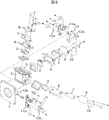
- FIGS. 9 shows a state in which the structure of a three-plate type solid-state imaging camera using three solid-state imaging elements is disassembled for each part.
- FIG. 10 shows a central horizontal section in a state where the parts shown in FIG. 9 are assembled.
- FIG. 10 is a side view of the assembled state of the components shown in FIG. 9.
- reference numeral 1 denotes a front frame of the camera housing
- 2 denotes a color separation prism.
- the color separation prism 2 separates light incident from an imaging lens (not shown) into light of three primary colors (red R, green G, and blue B) for each predetermined color component.
- Each decomposed light component is incident on each solid-state imaging device 3 and converted into an electrical signal.
- a prism surface fixing bracket 4 is bonded to each prism end surface of the color separation prism 2 for each separated light component, and an imaging element fixing lower bracket 5 is fastened with screws (not shown) thereon.
- an imaging element fixing upper metal fitting 6 is bonded to the back surface of each solid-state imaging element 3, and an imaging element heat conduction plate 7 for guiding the heat of the solid-state imaging element 3 to the outside is provided with screws (not shown). It has been stopped.
- the solid-state image pickup device 3 is soldered to the sensor substrate 8 with connection terminals such that the image pickup device fixing upper metal fitting 6 and the image pickup device heat conduction plate 7 are sandwiched between the back surface of the solid-state image pickup device 3 and the sensor substrate 8.
- the sensor substrate 8 is for taking out an electrical signal from the solid-state imaging device 3.
- the solid-state image sensor 3 soldered to the sensor substrate 8 has three primary colors of light (red R, green G, blue, with the image sensor fixing upper metal fitting 6 and the image sensor heat conduction plate 7 sandwiched between the back surfaces.
- Copper foil heat dissipating plates 11a and 11b are screwed to the image sensor heat conduction plate 7 for guiding the heat of the solid-state image sensor 3 to the outside and the semiconductor element heat conduction plate 10 for guiding the heat generated by the semiconductor element 9 to the outside.
- the copper foil heat sinks 11a and 11b are laminated in layers by thinly bonding a plurality of copper foils, and are cut and bent by pressing to further increase the flexibility of the copper foil heat sinks 11a and 11b. Several slits are provided for each bent portion.
- the copper foil heatsinks 11a and 11b guide the heat transferred to the front frame 1 of the camera housing, respectively, so that the copper support plates 12a and 12b installed on both side surfaces of the color separation prism 2 are respectively applied to the plate 13a. , 13b.
- heat generated from the solid-state imaging device 3 passes through the imaging device fixing upper bracket 6, the imaging device heat conduction plate 7, the copper foil radiator plate 11a, the copper support plate 12a, etc. Guided to the front frame 1.
- the heat generated from the signal processing semiconductor element 9 mounted on the rear surface of the sensor substrate 8 passes through the semiconductor element heat conduction plate 10, the copper foil heat radiating plate 11b, the copper support plate 12b, etc., and the front frame of the camera housing. Led to 1.
- the above-described prior art has the following problems. That is, in the solid-state imaging device, the positional relationship with respect to the color separation prism is fixed after precise three-dimensional optical position adjustment with respect to the color separation prism, but the light of the three primary colors (red R, green G, blue The position of the solid-state imaging device with respect to B) is determined after absorbing all of the dimensional tolerance, mounting dimensional tolerance, etc.
- the screw tightening torque is increased in order to reduce the contact thermal resistance of the screw fastening portion, the position of the screw fastening member is deviated, mechanical stress is applied to the solid-state imaging device, and registration deviation occurs. .
- the tightening torque at the time of screw tightening described above must be specified to be small, which deteriorates assemblability and heat transfer performance. End up.
- the present invention has been made to solve the problems associated with the prior art described above, and achieves at least one of the following objects.
- the first object of the present invention is to apply a large mechanical stress to the solder joint for fixing the sensor substrate even when the solid-state imaging device is mounted on the front surface of the sensor substrate and the semiconductor element for signal processing is mounted on the rear surface. It is an object of the present invention to provide an imaging apparatus including a cooling mechanism that can efficiently dissipate heat generated from the heating element.
- the second object of the present invention is to remove a large force, that is, a large mechanical stress from a heating element without applying a large mechanical stress to a solder joint for fixing a sensor substrate on which a heating element such as a solid-state imaging device or a signal processing semiconductor element is mounted.
- An object of the present invention is to provide an imaging apparatus including a cooling mechanism that can efficiently dissipate generated heat.
- a third object of the present invention is to generate heat generated from a heating element without applying a large mechanical stress to a solder joint for fixing a sensor substrate on which a heating element such as a solid-state imaging device or a signal processing semiconductor element is mounted.
- An object of the present invention is to provide a manufacturing method for easily assembling an imaging device having a cooling mechanism capable of efficiently radiating heat in a short time with high accuracy.
- a typical configuration of the present invention for achieving the first object is as follows.
- Has a housing outside the device separates light incident from the front of the device into a plurality of color components by a color separation prism, converts each color component into an electrical signal by a solid-state image sensor, and processes the converted electrical signal
- An image pickup apparatus that performs signal processing using a semiconductor element for image processing, comprising: a cooling mechanism that cools the solid-state image pickup element and the signal processing semiconductor element for each color component; and the solid-state image pickup element and the signal processing semiconductor element.
- Each of the sensor substrates is fixed by soldering at a solder joint provided in the imaging device casing, the solid-state imaging device is mounted on the front surface of the sensor substrate, and the sensor substrate One or a plurality of the signal processing semiconductor elements are mounted on the rear surface, and each of the cooling mechanisms is connected to the solid-state imaging element.
- a heat conductive sheet, and the first opening and the second opening And a filled thermal grease, the The first heat conductive sheet, the first heat conductive sheet, and the first heat radiator interposed between the sensor substrate, the first heat radiator, and the sensor substrate to generate heat from the solid-state imaging device.
- An image pickup apparatus comprising: a heat conduction grease interposed between a heat radiator and the heat conduction plate; and the heat conduction plate and the heat conduction plate that transmits the heat to the image pickup apparatus casing.
- the typical configuration of the present invention for achieving the second object is as follows.
- An imaging apparatus having a casing on the outside of the apparatus, converting light incident from the front of the apparatus into an electrical signal by a solid-state imaging device, and processing the converted electrical signal by a signal processing semiconductor element, the solid-state imaging
- the sensor substrate is provided with a solder joint provided in the imaging device casing.
- the solid-state image sensor is mounted on the front surface thereof, and one or more signal processing semiconductor elements are mounted on the front surface or the rear surface thereof.
- the cooling mechanism includes the solid-state image sensor.
- a heat conduction plate disposed behind the image sensor and fixed to the housing of the imaging device, and disposed in a first opening of the heat conduction plate and capable of floating in all directions including the front-rear direction in the first opening.
- Conductive grease is transmitted to the imaging device casing via the thermal conductive plate, and heat generated from the signal processing semiconductor element is interposed between the signal processing semiconductor element and the second heat radiator.
- the second heat conductive sheet having electrical insulation provided on the rear surface of the sensor substrate so as to be interposed between the sensor substrate, the second radiator and the sensor substrate, and the second heat conductive sheet Heat conduction grease interposed between the second heat radiator, the second heat radiator, the heat conduction grease interposed between the second heat radiator and the heat conduction plate, and the heat conduction plate.
- the imaging device is transmitted to the imaging device casing.
- a typical configuration of the present invention for achieving the third object is as follows.
- the solid-state imaging device is mounted on the front surface, and the sensor substrate on which one or more of the signal processing semiconductor devices are mounted on the front surface or the rear surface is positioned, and the sensor substrate is fixed in the imaging device casing.
- a heat conduction plate having a step, a first opening provided at a position facing the solid-state imaging device, and one or a plurality of second openings provided at a position facing the signal processing semiconductor element, Arranging behind the sensor substrate and fixing it to the imaging device casing, and floating in the first opening of the heat conducting plate in all directions including the front-rear direction in the first opening
- Step through the first heat dissipating body and the first heat conductive sheet having heat insulation between the first heat dissipating body and the sensor substrate and the heat conductive grease, the sensor by the elastic body Pressing the substrate against the signal processing semiconductor element by means of an elastic body through thermal conductive grease, or between the second radiator and the sensor substrate. And a step of pressing against the sensor substrate by an elastic body via a second heat conductive sheet having electrical insulation and a heat conductive grease.
- heat generated from a heating element can be efficiently dissipated without applying a large mechanical stress to a solder joint that fixes a sensor substrate on which a heating element such as a solid-state imaging device or a signal processing semiconductor element is mounted. can do.
- 1 is an exploded perspective view of a part of an imaging apparatus according to a first embodiment of the present invention. It is a disassembled perspective view explaining the method to fix the sensor board
- FIG. 1 is an exploded perspective view of a part of the imaging apparatus according to the first embodiment.
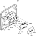
- FIG. 2 is an exploded perspective view for explaining a method of fixing the sensor substrate of the imaging apparatus according to the first embodiment to the color separation prism.
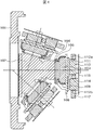
- FIG. 3 is a horizontal central cross-sectional view of the imaging apparatus according to the first embodiment.
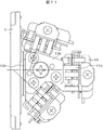
- FIG. 4 is a vertical sectional view of the imaging apparatus according to the first embodiment.
- reference numeral 101 denotes a front frame (front part of a housing) of a camera housing (imaging device housing) made of, for example, aluminum, and 102 denotes a color separation prism.
- a heat radiating fin is provided on the outer surface of the front frame 101.
- the color separation prism 102 separates light incident from a front imaging lens (not shown) into light of three primary colors (red R, green G, and blue B).
- the light components separated into the three primary colors are divided into three directions as shown in FIG. 1, and when viewed from the color separation prism 102, the R component is diagonally upward, the G component is horizontal, and the B component is diagonally downward.
- the light enters the solid-state image sensor 103 for R, G, and B, and is converted into an electric signal.
- the front means the direction in which light is incident, for example, the direction in which the front frame 101 is viewed from the color separation prism 102
- the rear means the opposite direction.
- the channel configuration for each light component that is, the fixing structure of the solid-state image sensor 103, the cooling mechanism for cooling the solid-state image sensor 103, and the like have the same configuration.
- the fixing structure and cooling mechanism of the solid-state imaging device 103 which is the configuration for the G component of the central channel of the primary color light (red R, green G, blue B), will be described, and the configuration related to the R component and B component that are other channels Will not be described.
- a prism surface fixing bracket 104 (for example, made by Permalloy) is bonded to the prism end face for each separated light component of the color separation prism 102, and an imaging element fixing lower bracket 105 (for example, made by Permalloy) is provided thereon. Is screwed.
- the solid-state imaging device 103 that extracts an electrical signal from light of three primary colors (red R, green G, and blue B) is mounted on the front surface of the sensor substrate 108 (for example, made of glass epoxy), and is mounted on the rear surface of the sensor substrate 108.
- the solid-state image sensor 103, the signal processing semiconductor element 109, and the signal connection connector 110 are soldered to the sensor substrate.
- the video signal is connected to the signal connection connector 110, and the color separation prism 102 is connected to the color separation prism 102 so that there is no chromatic aberration or image misalignment while viewing the video signal for each of the three primary colors (red R, green G, and blue B).
- the sensor substrate 108 on which the solid-state image sensor 103 is mounted is moved to perform positioning with a predetermined accuracy.
- the soldering lead 105a of the imaging element fixing lower metal fitting 105 is inserted into the solder fixing hole 108a of the sensor substrate 108, the soldering lead 105a is soldered to the solder fixing hole 108a in a positioned state, and solid-state imaging is performed.
- the position of the element 103 with respect to the color separation prism 102 is fixed.
- a light shielding member 117 made of flexible plastic or the like for preventing light incident from the outside of the color separation prism 102 is sandwiched between the color separation prism 102 and the solid-state imaging element 103.
- soldering lead 105a of the imaging element fixing lower metal fitting 105 is inserted into the solder fixing hole 108a of the sensor substrate 108 and soldered, the solder fixing is compared with the conventional soldering between flat surfaces shown in FIG. 9, for example. Solder creep at the solder joint between the hole 108a and the soldering lead 105a can be suppressed.
- the horizontal fixed cooling plate (heat conduction plate) 112 is perpendicular to the color separation prism 102 and the sensor substrate 108 so as to cover the color separation prism 102 and the sensor substrate 108 with a gap.
- the fixed cooling plates 122a and 122b and the front frame 101 are fixed to each other with screws.
- the horizontal fixed cooling plate (heat conductive plate) 112 and the vertical fixed cooling plates 122a and 122b are made of a high heat conductive metal having high heat conductivity, such as aluminum or copper.
- the horizontal fixed cooling plate 112 and the vertical fixed cooling plates 122a and 122b are used for the camera housing in which the color separation prism 102 is mounted to generate heat generated from the solid-state imaging device 103 and the signal processing semiconductor device 109 mounted on the sensor substrate 108. It is for guiding to the front frame 101.
- the plate spring 115 which is an elastic body, is screwed and fixed to the support column 108b provided upright on the sensor substrate 108 with a predetermined gap between the sensor substrate 108 and the plate spring 115. At this time, the screw for fixing the leaf spring 115 passes through the horizontal fixed cooling plate 112.
- the plate spring 115 may be fixed to the horizontal fixed cooling plate 112.
- the material of the saddle leaf spring 115 is, for example, phosphor bronze, and the thickness is, for example, 0.2 mm.
- the leaf spring 115 has a substantially rectangular frame shape (vertical 20 mm ⁇ horizontal 30 mm) when viewed from the front, a pressing portion 115 a that presses the radiator 113, which will be described later, and a pressing portion 115 b that presses the radiator 114 forward.
- the frame, the pressing part 115a and the pressing part 115b are integrally formed. By being integrally formed in this way, the load pressed by the leaf spring 115 does not generate solder crepes at the solder joint where the sensor substrate 108 is joined to the outside of the sensor substrate 108, or is registered in the solid-state image sensor 103. It is easy to manufacture a small leaf spring 115 that is small enough not to cause the deviation.
- the horizontal fixed cooling plate 112 is provided with a first opening 112a and a second opening 112b, each of which has, for example, an aluminum radiator 113 (one in the example of FIG. 1). And the radiator 114 (two in the example of FIG. 1) are accommodated so as to be movable in all directions including the front-rear direction.
- the omni-direction includes a front-rear direction, a direction perpendicular to the front-rear direction (up and down, left-right, oblique vertical direction), and an oblique direction with respect to the front-rear direction.
- the flange spring 115 urges the heat dissipating body 113 and the heat dissipating body 114 forward, and presses the signal processing semiconductor element 109 mounted on the rear surface of the sensor substrate 108 or the rear surface of the sensor substrate 108.
- the spring load of the leaf spring 115 at this time is set to a small value that does not cause solder crepe at the solder joint where the sensor substrate 108 is joined, or does not cause registration misalignment in the solid-state image sensor 103. 50 g or less.
- the horizontal fixed cooling plate 112 includes a first opening 112a for cooling the solid-state imaging device and a second opening 112b for cooling the semiconductor device, at positions facing the solid-state imaging device 103 and the signal processing semiconductor device 109, respectively. Is opened.
- the first opening 112a is a rectangular opening when viewed from the front (the shape viewed from the front), and the second opening 112b is a circular opening when viewed from the front.
- the first opening 112a and the second opening 112b are through holes of the same area that penetrate from the front surface to the rear surface of the horizontal fixed cooling plate 112, but are not limited to the through holes of the same area. .
- a first radiator 113 that is smaller than the opening size of the first opening 112a and can move in all directions including the front-rear direction in the first opening 112a is inserted and disposed.
- a signal connection connector 110 for taking out a video signal of the sensor substrate 108 is also inserted.
- the first heat dissipating body 113 is U-shaped when viewed from the front, and the U-shaped shape is determined so that the first heat dissipating body 113 does not interfere with the signal connection connector 110.
- the signal connector 110 is provided in the center of the sensor substrate 108 in order to take out the video signal at high speed.
- the solid-state image sensor 103 is usually mounted on the front surface of the sensor substrate 108 because it needs to face the color separation prism 102 side (front side) in order to take in image light. Therefore, heat generated from the solid-state image sensor 103 is taken from the rear surface of the sensor substrate 108 via the sensor substrate 108. Therefore, a U-shaped sheet 111, which is a thermal conductive sheet having electrical insulation and high thermal conductivity, is attached to the rear surface of the sensor substrate 108 so as to face the solid-state imaging device 103, and the rear surface of the sensor substrate 108 A U-shaped sheet 111 is sandwiched between the heat radiator 113.
- the U-shaped sheet 111 for example, a high thermal conductivity sheet (made of heat dissipation silicon rubber) having a thermal conductivity of 1 to 5 W / (m ⁇ K) can be used. Then, a small load is applied from the rear side of the first heat dissipating body 113 by the integrated leaf spring 115 so as to maintain a good contact of heat conduction between the U-shaped sheet 111 and the first heat dissipating body 113. I have to.
- the U-shaped sheet 111 has a U-shape when viewed from the front, and the U-shaped shape is determined so that the U-shaped sheet 111 does not interfere with the signal connection connector 110.
- the first heat dissipating body 113 can move in all directions including the front-rear direction, even if the U-shaped sheet 111 is attached with a slight inclination with respect to the rear surface of the sensor substrate 108, 1 heat radiator 113 can maintain a good thermal conductivity contact with the U-shaped sheet 111.
- the U-shaped sheet 111 prevents the heat conductive grease described later from coming into contact with the sensor substrate 108, and the heat conductive grease penetrates the sensor substrate 108 to change the sensor substrate 108. Play a role in preventing.
- the first opening 112a is filled with heat conductive grease that conducts heat efficiently and does not hinder the movement of the first radiator 113.
- This thermal conductive grease also serves as a lubricant that enhances the ease of movement.
- a high thermal conductive grease having a thermal conductivity of 1 to 5 W / (m ⁇ K) can be used.
- the gap between the horizontally fixed cooling plate 112 and the first radiator 113 in the first opening 112a is filled with the thermal conductive grease, and the heat of the first radiator 113 is efficiently horizontally fixed. It can be transmitted to the cooling plate 112.
- the thermal conductive grease is interposed between the U-shaped sheet 111 and the first heat radiator 113, the heat from the U-shaped sheet 111 can be efficiently transmitted to the first heat radiator 113. Can do. Therefore, the U-shaped sheet 111 having electrical insulation properties and high thermal conductivity efficiently derives the heat transferred from the solid-state imaging device 103 to the sensor substrate 108, and the derived heat is transmitted through the heat conduction grease. 1 to the heat radiator 113. Further, the heat from the first heat radiator 113 is efficiently transmitted to the horizontal fixed cooling plate 112 via the heat conductive grease.
- the second radiators 114 smaller than the opening size of the second openings 112b and capable of floating in all directions including the front-rear direction are inserted in the second openings 112b.
- the second heat radiator 114 has a circular columnar shape when viewed from the front.
- the second heat radiator 114 is in direct contact with the surface of the signal processing semiconductor element 109 mounted on the rear surface of the sensor substrate 108 via heat conductive grease, and is integrally formed from the rear of the second heat radiator 114.
- a small load by the plate spring 115 By applying a small load by the plate spring 115, a good heat conduction contact is maintained between the signal processing semiconductor element 109 and the second radiator 114.
- each signal processing semiconductor element 109 has a sensor substrate. Even when mounted at different angles or mounted at different angles with respect to the rear surface of the 108, each second radiator 114 maintains good contact with the corresponding signal processing semiconductor element 109 in heat conduction. be able to.
- the second opening 112b is filled with heat conductive grease having high heat conductivity that efficiently transfers heat and does not hinder the movement of the second heat radiator 114.
- the gap between the horizontally fixed cooling plate 112 and the second radiator 114 in the second opening 112b is filled with the thermal conductive grease, and the heat of the second radiator 114 is efficiently horizontally fixed. It can be transmitted to the cooling plate 112.
- the thermal conductive grease is interposed between the signal processing semiconductor element 109 and the second heat radiating body 114, heat from the signal processing semiconductor element 109 can be efficiently transmitted to the second heat radiating body 114. Can do. Therefore, the heat generated from the signal processing semiconductor element 109 is transmitted to the second heat radiating body 114 via the thermal conductive grease, and is transmitted from the second heat radiating body 114 to the horizontal fixed cooling plate 112 via the thermal conductive grease. Can do.
- the cooling mechanism of the solid-state imaging device 103 includes a U-shaped sheet 111, a U-shaped sheet 111, and a first radiator 113.
- the cooling mechanism of the signal processing semiconductor element 109 includes a thermal conductive grease between the signal processing semiconductor element 109 and the second radiator 114, a second radiator 114, a leaf spring 115, and a second radiator.
- the heat generated from the solid-state image sensor 103 is the sensor substrate 108, the U-shaped sheet 111, the heat conduction grease between the U-shaped sheet 111 and the first heat radiator 113, and the first heat radiator 113.
- the heat conduction grease between the first radiator 113 and the horizontal fixed cooling plate 112, the horizontal fixed cooling plate 112, the vertical fixed cooling plates 122a and 122b, etc., are efficiently transmitted to the front frame 101, and the solid-state image sensor 103 Can be cooled.
- the heat generated from the signal processing semiconductor element 109 is in parallel with the heat conduction grease between the signal processing semiconductor element 109 and the second heat dissipation element 114, the second heat dissipation element 114, and the second heat dissipation element 114. Through the heat conduction grease between the fixed cooling plates 112, the horizontal fixed cooling plate 112, the vertical fixed cooling plates 122a and 122b, etc., it is efficiently transmitted to the front frame 101, and the signal processing semiconductor element 109 can be cooled.
- the gap between the horizontal fixed cooling plate 112 and the first radiator 113 in the first opening 112a and the gap between the horizontal fixed cooling plate 112 and the second radiator 114 in the second opening 112b are as follows.
- the solid-state imaging device 103 or each member is set to a value that absorbs all dimensional tolerances, mounting dimensional tolerances, and the like and satisfies the cooling performance.
- the horizontal fixed cooling plate 112 is made of aluminum and has a thickness of 3 mm
- the gap may be selected from 100 to 200 ⁇ m.
- the solid-state imaging device 103 is mounted on the front surface side of the sensor substrate 108, and the signal processing semiconductor element 109 is mounted on the rear surface side of the sensor substrate 108.
- the heat generated from the heating element can be efficiently radiated to the imaging device housing without applying a large force to the sensor substrate 108 or the solder joint portion that is a fixing portion of the sensor substrate 108.
- the sensor substrate 108 is fixed by soldering, but the cooling mechanism of the first embodiment can be applied even when the sensor substrate 108 is fixed by an adhesive.
- the first opening 112a and the second opening 112b are formed as through holes, and the first heat dissipating body 113 and the second heat dissipating body 114 are pressed by the leaf spring 115 from the rear of the through holes.
- the first opening 112a and the second opening 112b can be formed as non-through holes (concave portions) whose rear surfaces are closed, and an elastic body such as a leaf spring or a coil spring can be provided on the rear surface in the holes.
- the following effects (1) to (10) can be obtained.
- the heat conduction grease between the first heat radiator 113, the heat conduction grease between the first heat radiator 113 and the horizontal fixed cooling plate 112, the horizontal fixed cooling plate 112, and the like can efficiently radiate heat.
- the solid-state imaging device 103 is mounted on the front surface of the sensor substrate 108, the signal processing semiconductor device 109 is mounted on the rear surface, and the heat from the solid-state imaging device 103 is transferred to the first heat dissipating body 113 via the heat conductive sheet 111. Since the heat from the signal processing semiconductor element 109 is transmitted to the second radiator 114 without going through the heat conductive sheet, the solid-state imaging element and the signal processing semiconductor element are mounted on the front surface of the sensor substrate. Compared with the configuration in which heat from the solid-state imaging device and the signal processing semiconductor device is transmitted to the heat radiating body through the heat conductive sheet, the heat radiation effect can be enhanced.
- the first heat dissipating body 113 can move in all directions including the front-rear direction, even if the U-shaped sheet 111 is attached with a slight inclination with respect to the rear surface of the sensor substrate 108, The heat dissipating body 113 can maintain good contact with the U-shaped sheet 111 in heat conduction.
- the second heat dissipator 114 can move in all directions including the front-rear direction, even if the signal processing semiconductor element 109 is mounted with a slight inclination with respect to the rear surface of the sensor substrate 108, The radiator 114 can maintain a good thermal conductivity contact with the signal processing semiconductor element 109.
- each of the signal processing semiconductor elements 109 is a sensor. Even when mounted in a different direction with respect to the rear surface of the substrate 108 or mounted at a different angle, each of the second radiators 114 has good contact with the corresponding signal processing semiconductor element 109 in heat conduction. Can keep.
- one horizontal fixed cooling plate 112 heat conduction plate
- a small cooling mechanism can be realized.
- the U-shaped sheet 111 prevents the thermal conductive grease from coming into contact with the sensor substrate 108, it is possible to prevent the thermal conductive grease from penetrating into the sensor substrate 108 and altering the sensor substrate 108. . Furthermore, since the U-shaped sheet 111 has electrical insulation, the electrical insulation of the sensor substrate 108 is ensured when the first heat radiator 113 is in contact therewith.
- the U-shaped sheet 111 has a U-shape when viewed from the front, it can be prevented from interfering with the signal connection connector 110, and a large contact area with the sensor substrate 108 can be realized.
- the solder lead 105a of the imaging element fixing lower metal fitting 105 is inserted into the solder fixing hole 108a of the sensor substrate 108 and soldered, compared with the conventional soldering between the flat surfaces shown in FIG. It is possible to suppress solder creep.
- the leaf spring 115 is integrally formed with a pressing portion 115a that presses the radiator 113 forward and a pressing portion 115b that presses the radiator 114 forward. Thus, it is easy to manufacture a small leaf spring 115 that is small enough not to generate solder crepe at the solder joint where the sensor substrate 108 is joined, or does not cause registration deviation in the solid-state image sensor 103.
- FIG. 5 is an exploded perspective view of a part of the imaging apparatus according to the second embodiment. 5 that are the same as those described in the first embodiment in FIG. Also, since the structures for the three primary colors of light (red R, green G, and blue B) are the same, only the middle G channel is shown and described in detail here.
- the solid-state imaging device 103 and the signal processing semiconductor device 209 are soldered to the front surface of the sensor substrate 208 that extracts an electrical signal.
- the sensor board 208 is the same as the sensor board 108 of the first embodiment in other respects, and a signal connection connector (not shown) for taking out the video signal of the solid-state image sensor 103 is provided on the rear surface of the sensor board 208. It has been.
- a horizontal fixed cooling plate 212 heat conduction plate
- vertical fixed cooling plates 122a and 122b and a front surface so as to cover the color separation prism 102 and the sensor substrate 208 with a gap outside the color separation prism 102 and the sensor substrate 208.
- the frame 101 is fixed to each other with screws.
- the horizontal fixed cooling plate 212 and the vertical fixed cooling plates 122a and 122b are made of a high heat conductive metal having high heat conductivity, such as aluminum or copper.
- the horizontal fixed cooling plate 212 and the vertical fixed cooling plates 122a and 122b are arranged in a camera housing in which the heat generated from the solid-state imaging device 103 and the signal processing semiconductor device 209 mounted on the sensor substrate 208 is mounted on the color separation prism 102. It is for guiding to the front frame 101.
- a leaf spring 215 that is an elastic body is screwed and fixed to a support 208b that is erected on the sensor substrate 208 at a predetermined interval from the sensor substrate 208. At this time, the screw for fixing the leaf spring 215 passes through the horizontal fixed cooling plate 212.
- the plate spring 215 may be fixed to the horizontal fixed cooling plate 212.
- the shape, material, and thickness of the leaf spring 215 are the same as those of the leaf spring 115 of the first embodiment.
- the horizontal fixed cooling plate 212 is provided with a third opening 212a, in which the radiator 213 is accommodated so as to be movable in all directions including the front-rear direction.
- the radiator 213 is biased forward by the leaf spring 215 and presses the rear surface of the sensor substrate 208.
- the load that pushes the leaf spring 215 at this time is the same as in the first embodiment, so that no solder crepe is generated at the solder joint where the sensor substrate 208 is joined to the outside, or the solid-state image sensor 103 is misaligned. It is set to be small enough not to generate and is 50 g or less.
- a third opening 212 a for cooling the solid-state image sensor 103 and the signal processing semiconductor element 209 is opened at a position facing the solid-state image sensor 103 and the signal processing semiconductor element 209.
- the third opening 212 a is a rectangular opening that is rectangular when viewed from the front, and is a through hole that penetrates from the front surface of the horizontal fixed cooling plate 212 to the rear surface.
- a third radiator 213 that is smaller than the opening size of the third opening 212a and can freely move in all directions including the front-rear direction in the third opening 212a is inserted and disposed.
- a signal connection connector (not shown) for taking out the video signal of the sensor substrate 208 is also inserted.
- the third radiator 213 has a square shape when viewed from the front, and an opening 213a, which is a rectangular through hole, is formed at the center thereof.
- the B-shaped shape of the third radiator 213 is determined so that the third radiator 213 does not interfere with the signal connection connector.
- the signal connection connector is provided at the center of the sensor substrate 208 in order to take out the video signal at high speed.
- the heat generated from the solid-state imaging device 103 and the signal processing semiconductor device 209 is taken from the rear surface of the sensor substrate 208 via the sensor substrate 208. Therefore, a square-shaped sheet 211 having electrical insulation and high thermal conductivity is sandwiched between the rear surface of the sensor substrate 208 and the third radiator 213. Then, a small load is applied from behind the third radiator 213 by the integral leaf spring 215 so as to maintain a good heat conduction contact between the B-shaped sheet 211 and the third radiator 213. I have to.
- the square-shaped sheet 211 has a square shape when viewed from the front, and a rectangular opening 211a is formed at the center thereof. The square shape of the square-shaped sheet 211 is determined so as not to interfere with the signal connection connector.
- the U-shaped sheet 211 plays a role of preventing the heat conductive grease having high thermal conductivity from coming into contact with the sensor substrate 208, similarly to the U-shaped sheet 111 of the first embodiment.
- the third opening 212a is filled with heat conductive grease having high heat conductivity that efficiently transfers heat and does not hinder the movement of the third radiator 213.
- the gap between the third opening 212a and the third heat radiating body 213 is filled with the heat conductive grease, and the heat of the third heat radiating body 213 can be efficiently transmitted to the horizontal fixed cooling plate 212. it can.
- the thermal conductive grease is interposed between the square-shaped sheet 211 and the third radiator 213, the heat from the square-shaped sheet 211 can be efficiently transmitted to the third radiator 213. Can do.
- the B-shaped sheet 211 having electrical insulation and high thermal conductivity efficiently derives the heat transmitted from the solid-state imaging device 103 and the signal processing semiconductor element 209 to the sensor substrate 208, and the derived heat is It is transmitted to the third heat radiating body 213 through the thermal conductive grease. Further, the heat from the third radiator 213 is transmitted to the horizontal fixed cooling plate 212 via the heat conductive grease.
- the material of the thermal conductive grease filled in the sensor substrate 208, the third heat radiator 213, the square-shaped sheet 211, and the third opening 212a is the sensor substrate 108 of the first embodiment, and the first The heat dissipating body 113, the U-shaped sheet 111, and the material of the heat conductive grease filled in the first opening 112a are the same.
- the cooling mechanism of the solid-state imaging device 103 and the signal processing semiconductor element 209 includes a B-shaped sheet 211, a B-shaped sheet 211, a third radiator 213, and the like.
- the solid-state imaging element 103 and the signal processing semiconductor element 209 can be cooled efficiently by being transmitted to the front frame 101.
- the cooling performance is slightly lower than that in the first embodiment, but since there are few cooling parts and the assembly is easy, the imaging apparatus can be assembled at low cost. There are features.
- FIG. 6 is an exploded perspective view illustrating a method for fixing the sensor substrate of the imaging apparatus according to the third embodiment to the color separation prism.
- the same configurations as those described in the first embodiment and the second embodiment are denoted by the same reference numerals and description thereof is omitted.
- Solder connection portions 305 a are formed at the four corners of the imaging element fixing lower metal fitting 305 attached to the eyelid prism 102.
- an image sensor fixing bracket 306 is fixed to the back surface of the solid-state image sensor 103 with an adhesive.
- Solder connection portions 306 a are also formed at the four corners of the image sensor fixing bracket 306.
- the solid-state image sensor 103 is mounted on the front surface of the sensor substrate 308, and the connection terminals of the solid-state image sensor 103 are soldered on the rear surface of the sensor substrate 308.
- each solid-state image sensor 103 is moved to perform positioning with a predetermined accuracy, and the solder connection portions 305a at the four corners of the imaging device fixing lower bracket 305 and the solder connection portions 306a at the four corners of the imaging device fixing bracket 306 are soldered and fixed. .
- the heat generated from the solid-state image sensor 103 is not released from the horizontal fixed cooling plate or the like to the front frame 301 via the sensor substrate 308 as in the first and second embodiments described above.
- the prism 102 can also escape from the prism 102 side through the imaging device fixing lower metal fitting 305.
- FIG. 7 is a horizontal central cross-sectional view of the imaging apparatus according to the fourth embodiment.
- FIG. 8 is a vertical sectional view of the imaging apparatus according to the fourth embodiment.
- the imaging element fixing lower metal fitting 405 is screwed to a front frame (front part of the casing) 401 of a camera casing (imaging apparatus casing) made of, for example, aluminum.
- the solid-state image sensor 403 is mounted on the front surface of the sensor substrate 408, and the connection terminal of the solid-state image sensor 403 is soldered on the rear surface of the sensor substrate 408.
- a signal processing semiconductor element 409 that processes a video signal of the solid-state imaging element 403 and a signal connection connector (not shown) that extracts a signal from the signal processing semiconductor element 409 are provided.
- the positioning of the solid-state image sensor 403 is performed as follows. That is, a video signal is connected to a signal connection connector (not shown), and the solid-state image sensor 403 is moved to perform positioning with a predetermined accuracy so that there is no image shift while viewing the video signal. At this time, since the soldering lead 405a of the imaging device fixing lower metal fitting 405 is inserted into the solder fixing hole (not shown) of the sensor substrate 408, the soldering lead 405a is inserted into the solder fixing hole (not shown) in this positioned state. Solder to). Thereby, the solid-state image sensor 403 is fixed to the front frame 401.
- the horizontal fixed cooling plate 412 heat conduction plate
- the vertical fixed cooling plates 422a and 422b and the front frame so as to cover the sensor substrate 408 with a gap outside the sensor substrate 408.
- 401 are fixed to each other by screws.
- the horizontal fixed cooling plate 412 (heat conductive plate) and the vertical fixed cooling plates 422a and 422b are made of a high heat conductive metal having high thermal conductivity, such as aluminum or copper.
- the horizontal fixed cooling plate 412 and the vertical fixed cooling plates 422a and 422b guide heat generated from the solid-state imaging device 403 and the signal processing semiconductor device 409 mounted on the sensor substrate 408 to the front frame 401 of the camera housing. belongs to.
- a plate spring 415 that is an elastic body is fixed to the horizontal fixed cooling plate 412 with screws.
- the shape, material, and thickness of the leaf spring 415 are the same as those of the leaf spring 115 of the first embodiment.
- the horizontal fixed cooling plate 412 is provided with a fourth opening 412a and a fifth opening 412b, in which the heat radiating body 413 and the heat radiating body 414 move in all directions including the front-rear direction. Accomodated as possible.
- the heat radiating body 413 and the heat radiating body 414 are urged forward by a leaf spring 415 and press the signal processing semiconductor element 409 mounted on the rear surface of the sensor substrate 408 or the rear surface of the sensor substrate 408.
- the spring load of the leaf spring 415 at this time does not cause a solder crepe to occur at the solder joint where the sensor substrate 408 is joined, or does not cause a registration shift in the solid-state image sensor 403, as in the first embodiment. It is set to a small one and is 50 g or less.
- the horizontal fixed cooling plate 412 has a fourth opening 412a for cooling the solid-state imaging element and a fifth opening 412b for cooling the semiconductor element at positions facing the solid-state imaging element 403 and the signal processing semiconductor element 409, respectively. And are opened.
- the fourth opening 412a is a rectangular opening that is rectangular when viewed from the front
- the fifth opening 412b is a circular opening that is circular when viewed from the front, both of which penetrate from the front surface to the rear surface of the horizontal fixed cooling plate 412. It is a through hole.
- a fourth heat radiating body 413 that is smaller than the opening size of the fourth opening 412a and can freely move in all directions including the front-rear direction in the fourth opening 412a is inserted and disposed.
- a signal connection connector (not shown) for taking out the video signal of the sensor substrate 408 is also inserted.
- the fourth radiator 413 is U-shaped when viewed from the front, like the first radiator 113 of the first embodiment, and this U-shaped configuration is such that the fourth radiator 413 is connected to the signal. It is determined not to interfere with the connector. Note that the signal connector is provided at the center of the sensor substrate 408 in order to take out the video signal at high speed.
- the fourth heat radiating body 413 can move in all directions including the front-rear direction, so that the U-shaped sheet 411 is attached with a slight inclination with respect to the rear surface of the sensor substrate 408.
- the fourth heat radiating body 413 can maintain good contact with the U-shaped sheet 411 in heat conduction.
- the U-shaped sheet 411 plays the role of preventing the thermal conductive grease from coming into contact with the sensor substrate 408, as in the first embodiment.
- the reason for the U-shape is that it does not interfere with the signal connection connector as in the first embodiment.
- the fourth opening 412a is filled with heat conductive grease having high heat conductivity that efficiently transfers heat and does not hinder the movement of the fourth heat radiating body 413.
- the gap between the horizontal fixed cooling plate 412 and the fourth radiator 413 in the fourth opening 412a is filled with the thermal grease, and the heat of the fourth radiator 413 is horizontally fixed efficiently. It can be transmitted to the cooling plate 412.
- the thermal conductive grease is interposed between the U-shaped sheet 411 and the fourth radiator 413, the heat from the U-shaped sheet 411 is efficiently transmitted to the fourth radiator 413. Can do.
- the U-shaped sheet 411 having electrical insulation and high thermal conductivity efficiently derives the heat transmitted from the solid-state imaging device 403 to the sensor substrate 408, and the derived heat is transmitted through the heat conduction grease. 4 radiating body 413. Furthermore, the heat from the fourth radiator 413 is efficiently transmitted to the horizontal fixed cooling plate 412 via the heat conductive grease.
- a fifth heat radiating body 414 that is smaller than the opening size of the fifth opening 412b and can move in all directions including the front-rear direction in the fifth opening 412b is inserted and disposed.
- the fifth radiator 414 has a circular columnar shape when viewed from the front.
- the fifth heat radiating body 414 is in direct contact with the surface of the signal processing semiconductor element 409 mounted on the rear surface of the sensor substrate 408 via heat conductive grease, and is integrally formed from the rear of the fifth heat radiating body 414. By applying a small load by the plate spring 415, a good heat conduction contact is maintained between the signal processing semiconductor element 409 and the fifth radiator 414.
- the fifth heat radiating body 414 can move in all directions including the front-rear direction, even if the signal processing semiconductor element 409 is mounted with a slight inclination with respect to the rear surface of the sensor substrate 408, The fifth radiator 414 can maintain good contact with the signal processing semiconductor element 409 in heat conduction.
- the fifth opening 412b is filled with high thermal conductive grease that efficiently transfers heat and does not hinder the movement of the fifth radiator 414.
- the gap between the horizontal fixed cooling plate 412 and the fifth radiator 414 in the fifth opening 412b is filled with the heat conductive grease, and the heat of the fifth radiator 414 is horizontally fixed efficiently. It can be transmitted to the cooling plate 412.
- the thermal conductive grease is interposed between the signal processing semiconductor element 409 and the fifth heat radiating body 414, the heat from the signal processing semiconductor element 409 is efficiently transmitted to the fifth heat radiating body 414. Can do.
- the heat generated from the signal processing semiconductor element 409 is transmitted to the fifth heat radiating body 414 via the thermal conductive grease, and is transmitted from the fifth heat radiating body 414 to the horizontal fixed cooling plate 412 via the thermal conductive grease.
- the material of the thermal conductive grease filled in the sensor substrate 408, the fourth radiator 413 and the fifth radiator 414, and the fourth opening 412a and the fifth opening 412b is the same as that of the first embodiment.
- the material of the thermal conductive grease filled in the sensor substrate 108, the first heat radiator 113, and the first opening 112a is the same.
- the cooling mechanism of the solid-state imaging device 403 includes a U-shaped sheet 411, a U-shaped sheet 411, and a fourth radiator 413.
- the cooling mechanism of the signal processing semiconductor element 409 includes a thermal conductive grease between the signal processing semiconductor element 409 and the fifth radiator 414, a fifth radiator 414, a leaf spring 415, and a fifth radiator 414.
- the heat generated from the solid-state image sensor 403 includes the sensor substrate 408, the U-shaped sheet 411 having thermal conductivity, the thermal conductive grease between the U-shaped sheet 411 and the fourth radiator 413, 4, heat conduction grease between the fourth heat radiating body 413 and the horizontal fixed cooling plate 412, the horizontal fixed cooling plate 412, the vertical fixed cooling plates 422 a and 422 b, and the like, and efficiently transmitted to the front frame 401. Therefore, the solid-state image sensor 403 can be cooled. Further, the heat generated from the signal processing semiconductor element 409 is fixed horizontally to the heat conductive grease between the signal processing semiconductor element 409 and the fifth heat radiating body 414, the fifth heat radiating body 414, and the fifth heat radiating body 414. The signal processing semiconductor element 409 can be cooled because it is efficiently transmitted to the front frame 401 via the heat conduction grease between the cooling plates 412, the horizontal fixed cooling plate 412, the vertical fixed cooling plates 422a and 422b, and the like.
- the gap between the horizontal fixed cooling plate 412 and the fourth radiator 413 in the fourth opening 412a and the gap between the horizontal fixed cooling plate 412 and the fifth radiator 414 in the fifth opening 412b are as follows.
- the solid-state imaging device 403 or each member is set to a value that absorbs all the dimensional tolerances, mounting dimensional tolerances, etc., and satisfies the cooling performance.
- the horizontal fixed cooling plate 412 is made of aluminum and has a thickness of 3 mm
- the gap may be selected from 100 to 200 ⁇ m.
- the solid-state imaging device 403 is mounted on the front surface side of the sensor substrate 408, and the signal processing semiconductor element 409 is mounted on the rear surface side of the sensor substrate 408. Also in the fourth embodiment, the heat generated from the heating element can be efficiently radiated to the imaging device housing without applying a large force to the solder joint for fixing the sensor substrate 408.
- the present invention is not limited to the above-described embodiments, and various modifications can be made without departing from the scope of the invention.
- the solid-state imaging device is mounted on the front surface of the sensor substrate and the signal processing semiconductor device is mounted on the rear surface.
- the solid-state imaging device signal processing semiconductor device is mounted on the sensor substrate. It can also be mounted on the front.
- the first invention relates to the imaging apparatus according to the first embodiment, has a housing on the outside of the apparatus, separates light incident from the front of the apparatus into a plurality of color components by a color separation prism, and An image pickup apparatus that converts each component into an electric signal by a solid-state image sensor, and performs signal processing on the converted electric signal by a signal processing semiconductor element, wherein the solid-state image sensor and the signal processing unit are each for each color component
- Each of the sensor substrates is soldered at a solder joint provided in the imaging device casing.
- the solid-state imaging device is mounted on the front surface of the sensor substrate, and one or more of the signal processing semiconductor elements are mounted on the rear surface of the sensor substrate.
- each of the cooling mechanisms includes a first opening provided at a position facing the solid-state imaging element and one or a plurality of first openings provided at a position facing the signal processing semiconductor element.
- a heat conduction plate having two openings, disposed behind the sensor substrate and fixed to the imaging device housing, and disposed in the first opening of the heat conduction plate.
- a first heat dissipating member that can move in all directions including the front-rear direction, and a second heat dissipating member arranged in the second opening of the heat conducting plate and movable in all directions including the front-rear direction in the second opening.
- a heat dissipating body an elastic body that presses the first heat dissipating element against the sensor substrate from the rear, and a second heat dissipating element from the rear against the signal processing semiconductor element, and the solid-state imaging element.
- a first heat conductive sheet having edge properties, and a heat conductive grease filled in the first opening and the second opening, The first heat conductive sheet, the first heat conductive sheet, and the first heat radiator interposed between the sensor substrate, the first heat radiator, and the sensor substrate to generate heat from the solid-state imaging device.
- a thermal conductive grease interposed between the first thermal radiator, the thermal conductive grease interposed between the first thermal radiator and the thermal conductive plate, and the thermal conductive plate through the thermal conductive plate.
- An image pickup apparatus comprising: a heat conduction grease interposed between a heat radiator and the heat conduction plate; and the heat conduction plate and the heat conduction plate that transmits the heat to the image pickup apparatus casing.
- a second invention relates to the imaging apparatus according to the second embodiment, has a housing on the outside of the apparatus, separates light incident from the front of the apparatus into a plurality of color components by a color separation prism, and converts each color component into An imaging device that converts an electrical signal by a solid-state image sensor and processes the converted electrical signal by a signal processing semiconductor element, the solid-state image sensor and the signal processing semiconductor element for each color component And a sensor board on which the solid-state imaging device and the signal processing semiconductor element are mounted. Each sensor board is fixed by soldering at a solder joint provided in the imaging device casing.
- the solid-state image sensor and one or more signal processing semiconductor elements are mounted on the front surface of the sensor substrate, and the respective cooling mechanisms are A first opening provided at a position facing the solid-state imaging element and one or a plurality of second openings provided at a position facing the signal processing semiconductor element; A heat conduction plate disposed and fixed to the imaging device casing; and a first heat conduction plate disposed in a first opening of the heat conduction plate and capable of floating in all directions including the front-rear direction in the first opening.
- a second radiator that is disposed in the second opening of the heat conducting plate and is movable in all directions including the front-rear direction in the second opening, and the first and second radiators
- An elastic body that presses the body against the sensor substrate from behind;
- a first heat conductive sheet having electrical insulation provided on the rear surface of the sensor substrate so as to face the solid-state imaging device;
- a second heat conductive sheet having electrical insulation provided on the rear surface of the sensor substrate so as to face the signal processing semiconductor element; and heat filled in the first opening and the second opening With conductive grease, The first heat conductive sheet, the first heat conductive sheet, and the first heat radiator interposed between the sensor substrate, the first heat radiator, and the sensor substrate to generate heat from the solid-state imaging device.
- the imaging device housing Imaging device for. Note that the first heat conductive sheet and the second heat conductive sheet may be integrally formed.
- a third invention relates to the imaging device of the first embodiment to the fourth embodiment, has a housing on the outside of the device, converts light incident from the front of the device into an electrical signal by a solid-state imaging device, An imaging apparatus that performs signal processing on the converted electrical signal using a signal processing semiconductor element, the cooling mechanism for cooling the solid-state imaging element and the signal processing semiconductor element, the solid-state imaging element, and the signal processing semiconductor element
- the sensor substrate is fixed by soldering to a solder joint provided in the imaging device casing, the solid-state imaging device is mounted on the front surface, and one is mounted on the front or rear surface.
- the cooling mechanism includes a first opening provided at a position facing the solid-state imaging element and the signal processing semiconductor elements.
- a heat conduction plate having one or a plurality of second openings provided at positions opposed to the sensor substrate, disposed behind the sensor substrate, and fixed to the imaging device housing; and A first radiator disposed in the first opening and capable of floating in the first opening in all directions including the front-rear direction; and the second opening disposed in the second opening of the heat conducting plate.
- a second heat radiating body capable of floating in all directions including the front-rear direction, and an elastic body that presses the first and second heat radiating bodies from the rear to the front
- a first heat conductive sheet having electrical insulation provided on the rear surface of the sensor substrate so that heat generated from the solid-state imaging device is interposed between the sensor substrate and the first heat radiator and the sensor substrate.
- Heat conductive grease interposed between the first heat conductive sheet and the first heat radiator, the first heat radiator, heat interposed between the first heat radiator and the heat conductive plate. Conductive grease is transmitted to the imaging device casing via the thermal conductive plate, and heat generated from the signal processing semiconductor element is interposed between the signal processing semiconductor element and the second heat radiator.
- the second heat conductive sheet having electrical insulation provided on the rear surface of the sensor substrate so as to be interposed between the sensor substrate, the second radiator and the sensor substrate, and the second heat conductive sheet Heat conduction grease interposed between the second heat radiator, the second heat radiator, the heat conduction grease interposed between the second heat radiator and the heat conduction plate, and the heat conduction plate.
- the imaging device is transmitted to the imaging device casing.
- a fourth invention is the imaging device according to the first to third inventions, wherein a signal connection connector is mounted on the rear surface of the sensor board, and the shape of the first opening viewed from the front is rectangular.
- the shape of the first heat radiating body as viewed from the front is a U shape or a B shape, and the U shape or the B shape does not interfere with the signal connection connector.
- 5th invention is an imaging device of 1st invention thru
- a sixth invention is the imaging device according to the first to fifth inventions, wherein soldering at the solder joint portion of the sensor substrate is performed in a solder fixing hole provided in the sensor substrate.
- An image pickup apparatus wherein soldering is performed by inserting a soldering lead protruding from a joint.
- the 7th invention is an imaging device of 1st invention thru
- the said elastic body is a press part which presses the said 2nd heat radiator and the press part which presses the said 1st heat radiator. Is a leaf spring integrally formed.
- An eighth invention is the imaging device according to the first to seventh inventions, wherein a plurality of the signal processing semiconductor elements are mounted on the sensor substrate so as to respectively correspond to the plurality of signal processing semiconductor elements.
- An image pickup apparatus comprising: a plurality of the second openings and a plurality of the second radiators.
- a ninth invention relates to the imaging device of the first to fourth embodiments, has a housing on the outside of the device, converts light incident from the front of the device into an electrical signal by a solid-state imaging device, An image pickup apparatus that performs signal processing of the converted electrical signal using a signal processing semiconductor element, wherein a cooling mechanism that cools the heating element including the solid-state imaging element and the signal processing semiconductor element, and a plurality of the heating elements are mounted.
- a sensor substrate fixed in the imaging device housing wherein the cooling mechanism has a plurality of openings respectively provided at positions facing the plurality of heating elements, and is disposed behind the sensor substrate and A heat conduction plate fixed to the imaging device casing; a heat dissipating body that is disposed in each opening of the heat conduction plate and is movable in the opening; An elastic body that presses the heat dissipating body from the rear to the front, and heat conduction grease interposed between the heat generating body and the heat dissipating member for generating heat from the heat generating body, the heat dissipating body, the heat dissipating body, and the Heat conduction grease interposed between the heat conduction plate, the heat conduction plate, and the heat conduction plate to transmit to the imaging device casing, or the heat generation from the heat generation body, the sensor substrate, the heat dissipation body, and the sensor An electrically insulating heat conductive sheet provided on the rear surface of the sensor substrate so as to be interposed between the substrates, a heat
- an image pickup apparatus having a housing on the outside of the saddle device, converting light incident from the front of the device into an electric signal by a solid-state image pickup device, and processing the converted electric signal by a signal processing semiconductor element.
- the solid-state imaging device is mounted on a front surface thereof, and one or a plurality of the signal processing semiconductor devices are mounted on the front surface or the rear surface of the sensor substrate, and the sensor substrate is positioned in the housing of the imaging device.
- heat generated from a heating element can be efficiently dissipated without applying a large mechanical stress to a solder joint that fixes a sensor substrate on which a heating element such as a solid-state imaging device or a signal processing semiconductor element is mounted. Therefore, it can be used for cooling a general electronic device or the like having a sealed housing.
Landscapes
- Engineering & Computer Science (AREA)
- Multimedia (AREA)
- Signal Processing (AREA)
- Physics & Mathematics (AREA)
- General Physics & Mathematics (AREA)
- Studio Devices (AREA)
- Transforming Light Signals Into Electric Signals (AREA)
- Color Television Image Signal Generators (AREA)
- Cooling Or The Like Of Semiconductors Or Solid State Devices (AREA)
- Solid State Image Pick-Up Elements (AREA)
Abstract
L'invention porte sur un appareil d'imagerie apte à dissiper efficacement de la chaleur générée par un élément générateur de chaleur tel qu'un dispositif de prise de vue à semi-conducteurs sans appliquer de contraintes mécaniques importantes sur des soudures qui fixent le substrat de capteur sur lequel l'élément générateur de chaleur est monté. L'appareil d'imagerie est configuré à partir de : un substrat de capteur, qui est fixé à l'intérieur du boîtier de l'appareil d'imagerie et sur lequel est monté l'élément générateur de chaleur ; une plaque thermoconductrice qui est fixée derrière le substrat de capteur et dans laquelle de multiples ouvertures sont ménagées ; des radiateurs qui sont agencés dans les ouvertures de la plaque thermoconductrice et sont aptes à se déplacer librement dans toutes les directions dans lesdites ouvertures ; de la graisse thermoconductrice remplissant l'espace entre la plaque thermoconductrice et les radiateurs, entre les radiateurs et l'élément générateur de chaleur, etc. ; une feuille themoconductrice placée entre le substrat de capteur et les radiateurs ; un corps élastique qui appuie les radiateurs sur le substrat de capteur depuis l'arrière ; etc. L'appareil d'imagerie est configuré de manière à ce que de la chaleur provenant de l'élément générateur de chaleur soit transmise au boîtier de l'appareil d'imagerie par les radiateurs, la feuille thermoconductrice, la graisse thermoconductrice et/ou la plaque thermoconductrice.
Priority Applications (1)
| Application Number | Priority Date | Filing Date | Title |
|---|---|---|---|
| KR1020137017165A KR101413869B1 (ko) | 2011-04-01 | 2012-03-16 | 촬상 장치 및 촬상 장치의 제조 방법 |
Applications Claiming Priority (2)
| Application Number | Priority Date | Filing Date | Title |
|---|---|---|---|
| JP2011082096A JP5813351B2 (ja) | 2011-04-01 | 2011-04-01 | 撮像装置及び撮像装置の製造方法 |
| JP2011-082096 | 2011-04-01 |
Publications (1)
| Publication Number | Publication Date |
|---|---|
| WO2012137586A1 true WO2012137586A1 (fr) | 2012-10-11 |
Family
ID=46749583
Family Applications (1)
| Application Number | Title | Priority Date | Filing Date |
|---|---|---|---|
| PCT/JP2012/056912 Ceased WO2012137586A1 (fr) | 2011-04-01 | 2012-03-16 | Appareil d'imagerie et procédé de production d'appareil d'imagerie |
Country Status (4)
| Country | Link |
|---|---|
| JP (1) | JP5813351B2 (fr) |
| KR (1) | KR101413869B1 (fr) |
| CN (1) | CN202424864U (fr) |
| WO (1) | WO2012137586A1 (fr) |
Cited By (1)
| Publication number | Priority date | Publication date | Assignee | Title |
|---|---|---|---|---|
| US11013148B2 (en) | 2018-07-24 | 2021-05-18 | Ricoh Company, Ltd. | Imaging apparatus |
Families Citing this family (1)
| Publication number | Priority date | Publication date | Assignee | Title |
|---|---|---|---|---|
| JP6595388B2 (ja) * | 2016-03-30 | 2019-10-23 | 京セラ株式会社 | 撮像モジュール |
Citations (4)
| Publication number | Priority date | Publication date | Assignee | Title |
|---|---|---|---|---|
| JPH0983878A (ja) * | 1995-09-14 | 1997-03-28 | Matsushita Electric Ind Co Ltd | 撮像素子の冷却装置 |
| JP2007208731A (ja) * | 2006-02-02 | 2007-08-16 | Sony Corp | 電子機器 |
| JP2011254261A (ja) * | 2010-06-01 | 2011-12-15 | Olympus Imaging Corp | 手振れ補正ユニット |
| JP2012049383A (ja) * | 2010-08-27 | 2012-03-08 | Nikon Corp | 撮像装置 |
Family Cites Families (3)
| Publication number | Priority date | Publication date | Assignee | Title |
|---|---|---|---|---|
| JPH05207486A (ja) * | 1992-01-30 | 1993-08-13 | Matsushita Electric Ind Co Ltd | 固体撮像装置 |
| JP2002247594A (ja) * | 2001-02-20 | 2002-08-30 | Olympus Optical Co Ltd | 撮像装置 |
| JP4964610B2 (ja) * | 2007-02-09 | 2012-07-04 | パナソニック株式会社 | 固体撮像素子の放熱構造及び固体撮像デバイス |
-
2011
- 2011-04-01 JP JP2011082096A patent/JP5813351B2/ja active Active
- 2011-12-29 CN CN2011205648845U patent/CN202424864U/zh not_active Expired - Fee Related
-
2012
- 2012-03-16 KR KR1020137017165A patent/KR101413869B1/ko not_active Expired - Fee Related
- 2012-03-16 WO PCT/JP2012/056912 patent/WO2012137586A1/fr not_active Ceased
Patent Citations (4)
| Publication number | Priority date | Publication date | Assignee | Title |
|---|---|---|---|---|
| JPH0983878A (ja) * | 1995-09-14 | 1997-03-28 | Matsushita Electric Ind Co Ltd | 撮像素子の冷却装置 |
| JP2007208731A (ja) * | 2006-02-02 | 2007-08-16 | Sony Corp | 電子機器 |
| JP2011254261A (ja) * | 2010-06-01 | 2011-12-15 | Olympus Imaging Corp | 手振れ補正ユニット |
| JP2012049383A (ja) * | 2010-08-27 | 2012-03-08 | Nikon Corp | 撮像装置 |
Cited By (1)
| Publication number | Priority date | Publication date | Assignee | Title |
|---|---|---|---|---|
| US11013148B2 (en) | 2018-07-24 | 2021-05-18 | Ricoh Company, Ltd. | Imaging apparatus |
Also Published As
| Publication number | Publication date |
|---|---|
| JP2012217094A (ja) | 2012-11-08 |
| KR101413869B1 (ko) | 2014-06-30 |
| KR20130105686A (ko) | 2013-09-25 |
| CN202424864U (zh) | 2012-09-05 |
| JP5813351B2 (ja) | 2015-11-17 |
Similar Documents
| Publication | Publication Date | Title |
|---|---|---|
| JP6176118B2 (ja) | 撮像ユニットおよび撮像装置 | |
| CN104954634B (zh) | 一种摄像模组及其制造方法 | |
| CN100592512C (zh) | 具有摄像元件的半导体装置 | |
| US20150031162A1 (en) | Photoelectric conversion device, image pickup system and method of manufacturing photoelectric conversion device | |
| WO2016009558A1 (fr) | Dispositif d'imagerie | |
| US8493503B2 (en) | Imaging apparatus | |
| JP6000337B2 (ja) | 撮像装置 | |
| JP2011091088A (ja) | 発熱体の放熱構造、および該放熱構造を用いた半導体装置 | |
| JP4903067B2 (ja) | 固体撮像素子の放熱構造 | |
| JP4890398B2 (ja) | 撮像装置 | |
| JP5813351B2 (ja) | 撮像装置及び撮像装置の製造方法 | |
| JP5640616B2 (ja) | 電子部品の放熱構造 | |
| JP4964610B2 (ja) | 固体撮像素子の放熱構造及び固体撮像デバイス | |
| JP6769087B2 (ja) | 冷却部材、冷却装置、電子機器および冷却部材の形成方法 | |
| JP4964704B2 (ja) | 撮像装置 | |
| JP2008198669A (ja) | 撮像装置及び撮像装置の製造方法 | |
| JP5427076B2 (ja) | 3ccd小型カメラの放熱構造 | |
| JP3606534B2 (ja) | 固体撮像装置 | |
| JP4182598B2 (ja) | 撮像装置 | |
| WO2026028383A1 (fr) | Dispositif de conversion d'énergie et procédé de fabrication de dispositif de conversion d'énergie | |
| JP2013201567A (ja) | 撮像装置および電子装置 | |
| JP2011151327A (ja) | 光モジュール及びその製造方法 | |
| WO2019021737A1 (fr) | Dispositif électronique | |
| WO2015097962A1 (fr) | Dispositif à semi-conducteur | |
| JP2009124622A (ja) | Ccd冷却構造、ccdカメラおよびccd冷却方法 |
Legal Events
| Date | Code | Title | Description |
|---|---|---|---|
| 121 | Ep: the epo has been informed by wipo that ep was designated in this application |
Ref document number: 12768588 Country of ref document: EP Kind code of ref document: A1 |
|
| ENP | Entry into the national phase |
Ref document number: 20137017165 Country of ref document: KR Kind code of ref document: A |
|
| NENP | Non-entry into the national phase |
Ref country code: DE |
|
| 122 | Ep: pct application non-entry in european phase |
Ref document number: 12768588 Country of ref document: EP Kind code of ref document: A1 |