WO2012137664A1 - Procédé de fabrication d'un moule - Google Patents
Procédé de fabrication d'un moule Download PDFInfo
- Publication number
- WO2012137664A1 WO2012137664A1 PCT/JP2012/058394 JP2012058394W WO2012137664A1 WO 2012137664 A1 WO2012137664 A1 WO 2012137664A1 JP 2012058394 W JP2012058394 W JP 2012058394W WO 2012137664 A1 WO2012137664 A1 WO 2012137664A1
- Authority
- WO
- WIPO (PCT)
- Prior art keywords
- layer
- mold
- aluminum
- aluminum alloy
- alloy layer
- Prior art date
- Legal status (The legal status is an assumption and is not a legal conclusion. Google has not performed a legal analysis and makes no representation as to the accuracy of the status listed.)
- Ceased
Links
Images



Classifications
-
- G—PHYSICS
- G02—OPTICS
- G02B—OPTICAL ELEMENTS, SYSTEMS OR APPARATUS
- G02B1/00—Optical elements characterised by the material of which they are made; Optical coatings for optical elements
- G02B1/10—Optical coatings produced by application to, or surface treatment of, optical elements
- G02B1/11—Anti-reflection coatings
- G02B1/118—Anti-reflection coatings having sub-optical wavelength surface structures designed to provide an enhanced transmittance, e.g. moth-eye structures
-
- B—PERFORMING OPERATIONS; TRANSPORTING
- B29—WORKING OF PLASTICS; WORKING OF SUBSTANCES IN A PLASTIC STATE IN GENERAL
- B29C—SHAPING OR JOINING OF PLASTICS; SHAPING OF MATERIAL IN A PLASTIC STATE, NOT OTHERWISE PROVIDED FOR; AFTER-TREATMENT OF THE SHAPED PRODUCTS, e.g. REPAIRING
- B29C33/00—Moulds or cores; Details thereof or accessories therefor
- B29C33/38—Moulds or cores; Details thereof or accessories therefor characterised by the material or the manufacturing process
-
- B—PERFORMING OPERATIONS; TRANSPORTING
- B29—WORKING OF PLASTICS; WORKING OF SUBSTANCES IN A PLASTIC STATE IN GENERAL
- B29C—SHAPING OR JOINING OF PLASTICS; SHAPING OF MATERIAL IN A PLASTIC STATE, NOT OTHERWISE PROVIDED FOR; AFTER-TREATMENT OF THE SHAPED PRODUCTS, e.g. REPAIRING
- B29C33/00—Moulds or cores; Details thereof or accessories therefor
- B29C33/42—Moulds or cores; Details thereof or accessories therefor characterised by the shape of the moulding surface, e.g. ribs or grooves
-
- C—CHEMISTRY; METALLURGY
- C25—ELECTROLYTIC OR ELECTROPHORETIC PROCESSES; APPARATUS THEREFOR
- C25D—PROCESSES FOR THE ELECTROLYTIC OR ELECTROPHORETIC PRODUCTION OF COATINGS; ELECTROFORMING; APPARATUS THEREFOR
- C25D1/00—Electroforming
- C25D1/10—Moulds; Masks; Masterforms
-
- C—CHEMISTRY; METALLURGY
- C25—ELECTROLYTIC OR ELECTROPHORETIC PROCESSES; APPARATUS THEREFOR
- C25D—PROCESSES FOR THE ELECTROLYTIC OR ELECTROPHORETIC PRODUCTION OF COATINGS; ELECTROFORMING; APPARATUS THEREFOR
- C25D11/00—Electrolytic coating by surface reaction, i.e. forming conversion layers
- C25D11/02—Anodisation
- C25D11/04—Anodisation of aluminium or alloys based thereon
-
- C—CHEMISTRY; METALLURGY
- C25—ELECTROLYTIC OR ELECTROPHORETIC PROCESSES; APPARATUS THEREFOR
- C25D—PROCESSES FOR THE ELECTROLYTIC OR ELECTROPHORETIC PRODUCTION OF COATINGS; ELECTROFORMING; APPARATUS THEREFOR
- C25D11/00—Electrolytic coating by surface reaction, i.e. forming conversion layers
- C25D11/02—Anodisation
- C25D11/04—Anodisation of aluminium or alloys based thereon
- C25D11/045—Anodisation of aluminium or alloys based thereon for forming AAO templates
-
- C—CHEMISTRY; METALLURGY
- C25—ELECTROLYTIC OR ELECTROPHORETIC PROCESSES; APPARATUS THEREFOR
- C25D—PROCESSES FOR THE ELECTROLYTIC OR ELECTROPHORETIC PRODUCTION OF COATINGS; ELECTROFORMING; APPARATUS THEREFOR
- C25D11/00—Electrolytic coating by surface reaction, i.e. forming conversion layers
- C25D11/02—Anodisation
- C25D11/04—Anodisation of aluminium or alloys based thereon
- C25D11/12—Anodising more than once, e.g. in different baths
-
- C—CHEMISTRY; METALLURGY
- C25—ELECTROLYTIC OR ELECTROPHORETIC PROCESSES; APPARATUS THEREFOR
- C25D—PROCESSES FOR THE ELECTROLYTIC OR ELECTROPHORETIC PRODUCTION OF COATINGS; ELECTROFORMING; APPARATUS THEREFOR
- C25D11/00—Electrolytic coating by surface reaction, i.e. forming conversion layers
- C25D11/02—Anodisation
- C25D11/04—Anodisation of aluminium or alloys based thereon
- C25D11/18—After-treatment, e.g. pore-sealing
- C25D11/24—Chemical after-treatment
-
- B—PERFORMING OPERATIONS; TRANSPORTING
- B29—WORKING OF PLASTICS; WORKING OF SUBSTANCES IN A PLASTIC STATE IN GENERAL
- B29C—SHAPING OR JOINING OF PLASTICS; SHAPING OF MATERIAL IN A PLASTIC STATE, NOT OTHERWISE PROVIDED FOR; AFTER-TREATMENT OF THE SHAPED PRODUCTS, e.g. REPAIRING
- B29C35/00—Heating, cooling or curing, e.g. crosslinking or vulcanising; Apparatus therefor
- B29C35/02—Heating or curing, e.g. crosslinking or vulcanizing during moulding, e.g. in a mould
- B29C35/08—Heating or curing, e.g. crosslinking or vulcanizing during moulding, e.g. in a mould by wave energy or particle radiation
- B29C35/0805—Heating or curing, e.g. crosslinking or vulcanizing during moulding, e.g. in a mould by wave energy or particle radiation using electromagnetic radiation
- B29C2035/0827—Heating or curing, e.g. crosslinking or vulcanizing during moulding, e.g. in a mould by wave energy or particle radiation using electromagnetic radiation using UV radiation
-
- B—PERFORMING OPERATIONS; TRANSPORTING
- B29—WORKING OF PLASTICS; WORKING OF SUBSTANCES IN A PLASTIC STATE IN GENERAL
- B29C—SHAPING OR JOINING OF PLASTICS; SHAPING OF MATERIAL IN A PLASTIC STATE, NOT OTHERWISE PROVIDED FOR; AFTER-TREATMENT OF THE SHAPED PRODUCTS, e.g. REPAIRING
- B29C59/00—Surface shaping of articles, e.g. embossing; Apparatus therefor
- B29C59/02—Surface shaping of articles, e.g. embossing; Apparatus therefor by mechanical means, e.g. pressing
- B29C59/04—Surface shaping of articles, e.g. embossing; Apparatus therefor by mechanical means, e.g. pressing using rollers or endless belts
- B29C59/046—Surface shaping of articles, e.g. embossing; Apparatus therefor by mechanical means, e.g. pressing using rollers or endless belts for layered or coated substantially flat surfaces
Definitions
- the present invention relates to a mold manufacturing method, and more particularly to a mold having a porous alumina layer on the surface.
- the “mold” here includes molds used in various processing methods (stamping and casting), and is sometimes referred to as a stamper. It can also be used for printing (including nanoprinting).
- An optical element such as a display device or a camera lens used for a television or a mobile phone is usually provided with an antireflection technique in order to reduce surface reflection and increase light transmission.
- an antireflection technique in order to reduce surface reflection and increase light transmission. For example, when light passes through the interface of a medium with a different refractive index, such as when light enters the interface between air and glass, the amount of transmitted light is reduced due to Fresnel reflection, and visibility is reduced. is there.
- This method utilizes the principle of a so-called moth-eye structure, and the refractive index for light incident on the substrate is determined from the refractive index of the incident medium along the depth direction of the irregularities, to the refractive index of the substrate.
- the reflection in the wavelength region that is desired to be prevented from being reflected is suppressed by continuously changing the wavelength.
- the moth-eye structure has an advantage that it can exhibit an antireflection effect with a small incident angle dependency over a wide wavelength range, can be applied to many materials, and can form an uneven pattern directly on a substrate. As a result, a low-cost and high-performance antireflection film (or antireflection surface) can be provided.
- Patent Documents 2 to 4 As a method for producing a moth-eye structure, a method using an anodized porous alumina layer obtained by anodizing aluminum is attracting attention (Patent Documents 2 to 4).
- anodized porous alumina layer obtained by anodizing aluminum will be briefly described.
- a method for producing a porous structure using anodization has attracted attention as a simple method capable of forming regularly ordered nano-sized cylindrical pores (fine concave portions).
- an acidic or alkaline electrolyte such as sulfuric acid, oxalic acid, or phosphoric acid
- a voltage is applied using the aluminum substrate as an anode
- oxidation and dissolution proceed simultaneously on the surface of the aluminum substrate.
- An oxide film having pores can be formed. These cylindrical pores are oriented perpendicular to the oxide film and exhibit self-organized regularity under certain conditions (voltage, type of electrolyte, temperature, etc.). Is expected.
- the porous alumina layer formed under specific conditions takes an array in which almost regular hexagonal cells are two-dimensionally filled with the highest density when viewed from the direction perpendicular to the film surface.
- Each cell has a pore in the center, and the arrangement of the pores has periodicity.
- the cell is formed as a result of local dissolution and growth of the film, and dissolution and growth of the film proceed simultaneously at the bottom of the pores called a barrier layer.
- the distance between adjacent pores corresponds to approximately twice the thickness of the barrier layer and is approximately proportional to the voltage during anodization.
- the diameter of the pores depends on the type, concentration, temperature, etc.
- the pores of such porous alumina have an arrangement with high regularity (having periodicity) under a specific condition, an arrangement with irregularity to some extent or an irregularity (having no periodicity) depending on the conditions. ).
- Patent Document 2 discloses a method of forming an antireflection film (antireflection surface) using a stamper having an anodized porous alumina film on the surface.
- Patent Document 3 discloses a technique for forming a tapered concave portion in which the pore diameter continuously changes by repeating anodization of aluminum and pore diameter enlargement processing.
- Patent Document 4 a technique for forming an antireflection film using an alumina layer in which fine concave portions have stepped side surfaces.
- an antireflection film (antireflection surface) is provided by providing a concavo-convex structure (macro structure) larger than the moth eye structure in addition to the moth eye structure (micro structure). ) Can be given an anti-glare (anti-glare) function.
- the two-dimensional size of the projections that form the projections and depressions that exhibit the antiglare function is 1 ⁇ m or more and less than 100 ⁇ m.
- a mold for forming a moth-eye structure on the surface (hereinafter referred to as “moth-eye mold”) can be easily manufactured.
- the surface of an anodized aluminum film is used as it is as a mold, the effect of reducing the manufacturing cost is great.
- the surface structure of the moth-eye mold that can form the moth-eye structure is referred to as an “inverted moth-eye structure”.
- a method using a photocurable resin is known. First, a photocurable resin is applied on the substrate. Subsequently, the uneven surface of the surface of the moth-eye mold is filled with the photocurable resin by pressing the uneven surface of the moth-eye mold subjected to the release treatment against the photocurable resin in a vacuum. Subsequently, the photocurable resin in the concavo-convex structure is irradiated with ultraviolet rays to cure the photocurable resin.
- the moth-eye mold described above is formed on an aluminum substrate represented by a substrate formed of aluminum or a cylinder formed of aluminum, or a support formed of a material other than aluminum typified by a glass substrate. It can be manufactured using an aluminum film. However, when a moth-eye mold is manufactured using an aluminum film formed on a glass substrate or plastic film, the aluminum film (partially an anodized film) is bonded to the glass substrate or plastic film. May decrease.
- the applicant of the present invention forms the inorganic underlayer (for example, SiO 2 layer) and the buffer layer (for example, AlO x layer) containing aluminum on the surface of the substrate formed of glass or plastic. It discovered that the fall of adhesiveness was suppressed and it is disclosing in patent document 5.
- a cylindrical moth-eye mold is formed, for example, by forming an organic insulating layer on the outer peripheral surface of a metal cylinder and alternately repeating anodization and etching on the aluminum film formed on the organic insulating layer. Is done. Also in this case, the adhesiveness can be improved by forming the inorganic underlayer and the buffer layer disclosed in Patent Document 5.
- Patent Documents 1, 2, 4, and 5 All the disclosures of Patent Documents 1, 2, 4, and 5 are incorporated herein by reference.
- the aluminum film formed on the organic insulating layer often contains abnormal particles.
- the abnormal particles are formed by abnormal growth of aluminum crystals.
- the aluminum film is a collection of crystal grains having an average grain size (average grain size) of about 200 nm, whereas the grain size of abnormal particles is larger than the average grain size and may be 500 nm or more.
- the organic insulating layer has a lower thermal conductivity than other materials (metal materials and inorganic insulating films), the aluminum film tends to be relatively hot during the aluminum film deposition process (for example, sputtering or vapor deposition). As a result, it is considered that abnormal growth of crystal grains is likely to occur, that is, abnormal particles are easily formed.
- Such a phenomenon can also occur when an aluminum film is directly deposited on the surface of an aluminum tube (for example, a thickness of 1 mm or more).
- a structure corresponding to the abnormal particles is formed on the surface of the porous alumina layer of the moth-eye mold.
- the structure corresponding to the abnormal particles is transferred to the surface of the antireflection film, which is caused by the abnormal particles transferred to the surface of the antireflection film.
- Light is scattered by the structure. That is, the antireflection film has haze.
- an antiglare function is imparted to the antireflection film, there may be no problem even if the antireflection film has haze due to abnormal particles, but the antireflection film does not have an antiglare function. There is a problem that cannot be manufactured.
- it is difficult to control the formation density (occurrence frequency) of abnormal particles it is preferable to suppress the generation of abnormal particles from the viewpoint of mass productivity.
- the present invention has been made to solve the above-mentioned problems, and its main purpose is to make it difficult for abnormal particles to be generated in an aluminum film in a method of manufacturing a mold using an aluminum film.
- An object of the present invention is to provide a mold manufacturing method capable of forming an antireflection film having no haze.
- an object of the present invention is to make it difficult for abnormal particles to be generated in an aluminum film in a mold manufacturing method using an aluminum film formed on an organic insulating film.
- a mold manufacturing method includes a mold having an inverted moth-eye structure on the surface having a plurality of recesses having a two-dimensional size of 10 nm or more and less than 500 nm when viewed from the normal direction of the surface.
- a mold substrate having a metal substrate, an organic insulating layer formed on the metal substrate, and an aluminum alloy layer formed on the organic insulating layer.
- the aluminum alloy layer contains aluminum and a metal element M other than aluminum, and the absolute value of the difference between the standard electrode potential of the metal element M and the standard electrode potential of aluminum is 0.64 V or less, A content of the metal element M in the alloy layer does not exceed 10% by mass, a step of preparing a mold base, and (b) a plurality of fine particles by partially anodizing the aluminum alloy layer A step of forming a porous alumina layer having a recess; and (c) after the step (b), the porous alumina layer is brought into contact with an etching solution to enlarge the plurality of fine recesses of the porous alumina layer. And (d) after the step (c), further anodizing to grow the plurality of fine recesses.
- the mold base prepared in the step (a) may be a mold base having a metal base (for example, an aluminum tube) and an aluminum alloy layer directly formed on the metal base.
- the mold base further includes an inorganic underlayer between the organic insulating layer and the aluminum alloy layer.
- the mold base further includes a buffer layer between the inorganic base layer and the aluminum alloy layer, and the buffer layer includes aluminum, the metal element M, oxygen, or nitrogen. including.
- the thickness of the buffer layer is preferably 10 nm or more and 500 nm or less.
- the aluminum and metal element M contents in the buffer layer have a higher profile on the aluminum alloy layer side than on the inorganic base layer side.
- the inorganic underlayer is a silicon oxide layer or a titanium oxide layer. In one embodiment, the thickness of the inorganic underlayer is preferably 50 nm or more and 300 nm or less.
- the organic insulating layer is an electrodeposition layer.
- the metal substrate is cylindrical, and the organic insulating layer is formed on an outer peripheral surface of a cylinder of the metal substrate.
- step (b) and the step (c) are further performed after the step (d).
- abnormal particles can be hardly generated in the aluminum film, and further, an antireflection film having no unnecessary haze can be formed.
- a possible mold manufacturing method is provided.
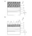
- (A) is a schematic diagram which shows the mold base material 10 used for manufacture of the type
- (b) is a schematic diagram which shows the mold 100 for moth eyes manufactured using the mold base material 10 It is.
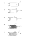
- (A)-(e) is a figure which shows the process of the manufacturing method of the roll type
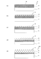
- (A)-(e) is a figure which shows the process of the manufacturing method of the type
- the mold of the present embodiment is a moth-eye mold, and has an inverted moth-eye structure on the surface having a plurality of recesses having a two-dimensional size of 10 nm or more and less than 500 nm when viewed from the normal direction of the surface. .
- a mold manufacturing method includes a metal base 72m, an organic insulating layer 13 formed on the metal base 72m, and an organic insulating layer 13 as shown in FIG. Including a step of preparing a mold base 10 having the aluminum alloy layer 18 formed.
- the metal substrate 72m and the organic insulating layer 13 may be collectively referred to as the support 12.
- the aluminum alloy layer 18 contains aluminum and a metal element M other than aluminum, and the absolute value of the difference between the standard electrode potential of the metal element M and the standard electrode potential of aluminum is 0.64 V or less.
- the content of the metal element M in the alloy layer 18 does not exceed 10% by mass.
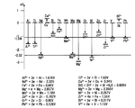
- the metal elements whose absolute value of the difference from the standard electrode potential of aluminum is 0.64 V or less are Ti, Nd, Mn, Mg, Zr, V, Pb, and the like.
- a target of an aluminum alloy containing Ti, Nd and Zr is commercially available and can be easily obtained.
- FIG. 19 is based on a physics and chemistry dictionary (Iwanami Shoten).
- the aluminum alloy layer 18 containing the metal element M has a reflectance of 80% or more in the wavelength range of 400 nm to 700 nm. That is, by containing the metal element M, abnormal growth of aluminum crystal grains is suppressed, and as a result, the aluminum alloy layer 18 contains almost no abnormal particles. Therefore, by using the aluminum alloy layer 18 to form the moth-eye mold 100 having the porous alumina layer 20 as shown in FIG. 1B, there is no unnecessary haze (no haze or no haze). A mold 100 capable of forming an antireflection film (in which control is performed) can be obtained.
- the anodic oxidation process and the etching process may be alternately repeated on the aluminum alloy layer 18. Corrosion does not occur.
- Patent Document 6 a method for producing a moth-eye mold using an aluminum base material (a plate-like, cylindrical or columnar bulk aluminum having a thickness of 2 mm or more that can be self-supported). Disclosure.
- an aluminum base material a plate-like, cylindrical or columnar bulk aluminum having a thickness of 2 mm or more that can be self-supported.
- galvanic corrosion local cell reaction
- pits A dimple is formed.
- the pits are larger than the fine recesses inherent in the porous alumina layer and cause haze in the antireflection film.
- Patent Document 6 describes that in order to prevent this, it is preferable to use an aluminum base material that does not contain any element nobler than aluminum and contains Mg, which is a base metal rather than aluminum, as an impurity element. ing.
- the aluminum alloy layer 18 used in the embodiment according to the present invention is a known method (for example, an electron beam) in the same manner as a conventional aluminum layer formed using high-purity aluminum (purity of 99.99 mass% or more). (Evaporation method or sputtering method).
- the thickness of the aluminum alloy layer 18 is preferably 100 nm or more, and preferably 3000 nm or less from the viewpoint of productivity, in order to obtain an anodized alumina layer having a surface structure serving as a moth-eye mold. Typically, it is about 1000 nm (1 ⁇ m).
- the aluminum alloy layer 18 having a thickness of about 1 ⁇ m is deposited in a plurality of times rather than in a single deposition. That is, rather than continuously depositing to a desired thickness (for example, 1 ⁇ m), the process of interrupting the deposition to a certain thickness and restarting the deposition after a certain time has elapsed is repeated. It is preferable to obtain the aluminum alloy layer 18. For example, it is preferable to interrupt each time an aluminum alloy layer having a thickness of 50 nm is deposited and to obtain an aluminum alloy layer 18 having a thickness of about 1 ⁇ m by 20 aluminum alloy layers each having a thickness of 50 nm.
- the quality (for example, chemical resistance and adhesiveness) of the finally obtained aluminum alloy layer 18 can be improved by dividing the deposition of the aluminum alloy into a plurality of times.
- the continuous deposition of the aluminum alloy increases the temperature of the substrate (which has the surface on which the aluminum alloy layer is deposited), resulting in a distribution of thermal stress in the aluminum alloy layer 18 and the film This is considered to reduce the quality.
- an inorganic underlayer 14 between the organic insulating layer 13 and the aluminum alloy layer 18 as in the mold base 10 shown in FIG.
- the inorganic underlayer 14 is directly formed on the surface of the organic insulating layer 13 and functions to improve the adhesion between the organic insulating layer 13 and the aluminum alloy layer 18.
- the inorganic underlayer 14 is preferably formed of an inorganic oxide or an inorganic nitride.
- an inorganic oxide for example, a silicon oxide layer or a titanium oxide layer is preferable, and when an inorganic nitride is used, for example, a silicon nitride layer. Is preferred.
- the thermal expansion coefficient may be adjusted by adding impurities to the inorganic oxide layer or the inorganic nitride layer.
- the thermal expansion coefficient can be increased by adding germanium (Ge), phosphorus (P), or boron (B).
- the thickness of the inorganic underlayer 14 is preferably 40 nm or more, and more preferably 100 nm or more. If the thickness of the inorganic underlayer 14 is less than 40 nm, the effect of providing the inorganic underlayer 14 may not be sufficiently exhibited.
- the thickness of the inorganic underlayer 14 is preferably 500 nm or less, and more preferably 200 nm or less. If the thickness of the inorganic underlayer 14 exceeds 500 nm, the formation time of the inorganic underlayer 14 becomes unnecessarily long. Also, the thicker the inorganic underlayer 14 formed on a curved surface or a flexible surface, the easier it is to crack.
- the mold substrate 10 preferably further includes a buffer layer 16 between the inorganic base layer 14 and the aluminum alloy layer 18.
- the buffer layer 16 acts to improve the adhesion between the inorganic underlayer 14 and the aluminum alloy layer 18.
- a conductive layer preferably a valve metal layer
- a conductive layer may be provided between the two.
- the buffer layer 16 preferably contains aluminum, a metal element M, and oxygen or nitrogen.
- the oxygen or nitrogen content may be constant, but it is particularly preferable that the aluminum and metal element M content has a higher profile on the aluminum alloy layer 18 side than on the inorganic underlayer 14 side. It is because it is excellent in matching of physical property values such as thermal expansion coefficient.
- the thickness of the buffer layer 16 is preferably 10 nm or more, and more preferably 20 nm or more. Further, the thickness of the buffer layer 16 is preferably 500 nm or less, and more preferably 200 nm or less. If the thickness of the buffer layer 16 is less than 10 nm, sufficient adhesion may not be obtained between the inorganic underlayer 14 and the aluminum alloy layer 18. Further, if the thickness of the buffer layer 16 exceeds 500 nm, the formation time of the buffer layer 16 becomes unnecessarily long, which is not preferable.
- the profile in the thickness direction of the aluminum content in the buffer layer 16 may change stepwise or may change continuously.
- the buffer layer 16 is formed of aluminum, the metal element M, and oxygen, a plurality of aluminum oxide alloy layers whose oxygen content gradually decreases are formed, and the aluminum alloy layer 18 is formed on the uppermost layer.
- the oxygen content of the buffer layer 16 is preferably 60 at% or less at the highest. The same applies to the case where the buffer layer 16 containing nitrogen instead of oxygen is formed.
- a porous alumina layer 20 having a plurality of fine recesses 22 is formed by partially anodizing the aluminum alloy layer 18 using the mold base 10 shown in FIG.
- the moth-eye mold 100 shown in FIG. 1 (b) can be obtained by performing the step of growing the minute recesses 22 of FIG.
- the moth-eye mold 100 is suitably used for manufacturing an antireflection film (antireflection surface).
- the cross-sectional shape of the fine recesses (pores) 22 of the porous alumina layer 20 used for manufacturing the antireflection film is generally conical.
- the fine recess 22 may have a stepped side surface.
- the two-dimensional size (opening diameter: D p ) of the fine recess 22 is preferably 10 nm or more and less than 500 nm, and the depth (D depth ) is preferably about 10 nm or more and less than 1000 nm (1 ⁇ m).
- D p opening diameter
- D depth is preferably about 10 nm or more and less than 1000 nm (1 ⁇ m).
- the bottom part of the fine recessed part 22 is pointed (the bottom part is a point).
- the fine concave portions 22 are closely packed, and assuming that the shape of the fine concave portions 22 when viewed from the normal direction of the porous alumina layer 20 is a circle, adjacent circles overlap each other, It is preferable that a brim is formed between the adjacent fine recesses 22.
- the substantially conical minute concave portions 22 are adjacent so as to form a collar portion, the two-dimensional size D p of the fine concave portions 22 is assumed to be equal to the average adjacent distance D int .
- the roll mold was prepared by the method described in International Publication No. 2011/105206 by the applicant.
- a stainless steel or nickel metal sleeve was used.
- the metal sleeve refers to a metal cylinder having a thickness of 0.02 mm to 1.0 mm.
- the entire disclosure of WO 2011/105206 is incorporated herein by reference.
- a metal sleeve 72m is prepared.
- the organic insulating layer 13 is formed on the outer peripheral surface of the metal sleeve 72m by, for example, an electrodeposition method.
- the electrodeposition method for example, a known electrodeposition coating method can be used. For example, first, the metal sleeve 72m is cleaned. Next, the metal sleeve 72m is immersed in an electrodeposition tank in which an electrodeposition liquid containing an electrodeposition resin is stored. Electrodes are installed in the electrodeposition tank. When the insulating resin layer is formed by cationic electrodeposition, the metal sleeve 72m is used as a cathode, the electrode installed in the electrodeposition tank is used as an anode, a current is passed between the metal sleeve 72m and the anode, and the metal sleeve 72m is used. An insulating resin layer is formed by depositing an electrodeposition resin on the outer peripheral surface of the film.
- the insulating resin layer is formed by anion electrodeposition, the insulating resin layer is formed by flowing an electric current with the metal sleeve 72m as an anode and the electrode installed in the electrodeposition tank as a cathode. Then, the organic insulating layer 13 is formed by performing a washing
- the electrodeposition resin for example, a polyimide resin, an epoxy resin, an acrylic resin, a melamine resin, a urethane resin, or a mixture thereof can be used.
- the organic insulating layer 13 can be formed by forming an insulating resin layer using various coating methods and curing as necessary. The organic insulating layer 13 has a high effect of flattening the surface, and it is possible to suppress the surface scratches of the metal sleeve 72 m and the like from being reflected on the surface shape of the aluminum alloy layer 18.
- the inorganic base layer 14 is formed on the organic insulating layer 13.
- the SiO 2 layer 14 having a thickness of about 100 nm is formed.
- the buffer layer 16 and the aluminum alloy layer 18 are formed continuously.
- the same target is used to form the buffer layer 16 and the aluminum alloy layer 18. Therefore, the ratio of aluminum to the metal element M is constant in the buffer layer 16 and the aluminum alloy layer 18.
- the buffer layer 16 has a thickness of, for example, about 100 nm, and the aluminum alloy layer 18 has a thickness of about 1 ⁇ m.
- the formation from the inorganic underlayer 14 to the formation of the aluminum alloy layer 18 is preferably performed by a thin film deposition method (for example, sputtering), and is preferably performed in the same chamber.
- the porous alumina layer 20 having a plurality of fine recesses is formed on the surface of the aluminum alloy layer 18 by alternately repeating anodic oxidation and etching.
- the mold 100a is obtained.
- FIG. 3 the mold base 10 is shown in which the aluminum alloy layer 18 is directly formed on the support 12.
- the mold substrate 10 includes a metal substrate, an organic insulating layer 13 formed on the metal substrate, and an aluminum alloy layer 18 deposited on the organic insulating layer 13.
- the porous alumina layer 20 includes a porous layer having fine concave portions 22 and a barrier layer.
- the porous alumina layer 20 is formed, for example, by anodizing the surface 18s in an acidic electrolytic solution.
- the electrolytic solution used in the step of forming the porous alumina layer 20 is, for example, an aqueous solution containing an acid selected from the group consisting of oxalic acid, tartaric acid, phosphoric acid, chromic acid, citric acid, and malic acid.
- the pore spacing, pore depth, pore shape, and the like can be adjusted.
- the thickness of the porous alumina layer can be changed as appropriate.
- the aluminum alloy layer 18 may be completely anodized.
- the porous alumina layer 20 is brought into contact with an alumina etchant to be etched by a predetermined amount, thereby enlarging the hole diameter of the fine recess 22.
- an alumina etchant to be etched by a predetermined amount, thereby enlarging the hole diameter of the fine recess 22.
- the amount of etching (that is, the size and depth of the fine recess 22) can be controlled by adjusting the type / concentration of the etching solution and the etching time.
- the etching solution for example, an aqueous solution of 10% by mass of phosphoric acid, an organic acid such as formic acid, acetic acid or citric acid, or a mixed solution of chromium phosphoric acid can be used.
- the aluminum alloy layer 18 is partially anodized again to grow the fine recesses 22 in the depth direction and to thicken the porous alumina layer 20.
- the side surface of the fine recess 22 is stepped.
- the porous alumina layer 20 is further etched by bringing the porous alumina layer 20 into contact with an alumina etchant to further expand the hole diameter of the fine recess 22.
- an alumina etchant it is preferable to use the above-described etchant, and in practice, the same etch bath may be used.
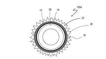
- a moth-eye mold 100A having a porous alumina layer 20 having a desired concavo-convex shape is obtained as shown in FIG.
- the side surface of the fine recess 22 can be stepped, or can be a smooth curved surface or a slope.
- the roll-shaped mold has an advantage that the surface structure of the mold can be continuously transferred to a work piece (having a surface on which an antireflection film is formed) by rotating the roll-shaped mold about an axis.
- An antireflection film manufacturing method includes a step of preparing the mold, a step of preparing a workpiece, and applying a photocurable resin between the mold and the surface of the workpiece. In this state, it includes a step of curing the photocurable resin by irradiating the photocurable resin with light and a step of peeling the mold from the antireflection film formed of the cured photocurable resin.
- an antireflection film can be produced by a roll-to-roll method.
- the film preferably includes a base film and a hard coat layer formed on the base film, and the antireflection film is preferably formed on the hard coat layer.
- the base film for example, a TAC (triacetyl cellulose) film can be suitably used.
- the hard coat layer for example, an acrylic hard coat material can be used.
- a mold 100A shown in FIG. 4 has a buffer layer 16 formed on the support 12.
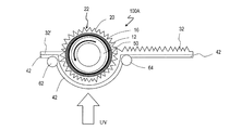
- FIG. 5 is a schematic cross-sectional view for explaining a method for producing an antireflection film by a roll-to-roll method.
- the roll-shaped moth-eye mold 100A shown in FIG. 4 is prepared.
- the ultraviolet curable resin 32 ′ is irradiated with ultraviolet rays (UV) in a state where the workpiece 42 having the ultraviolet curable resin 32 ′ applied to the surface thereof is pressed against the moth-eye mold 100 ⁇ / b> A.
- the ultraviolet curable resin 32 ' is cured.
- an acrylic resin can be used as the ultraviolet curable resin 32 ′.
- the workpiece 42 is, for example, a TAC (triacetyl cellulose) film.
- the workpiece 42 is unwound from an unillustrated unwinding roller, and then an ultraviolet curable resin 32 ′ is applied to the surface by, for example, a slit coater.
- the workpiece 42 is supported by support rollers 62 and 64 as shown in FIG.
- the support rollers 62 and 64 have a rotation mechanism and convey the workpiece 42. Further, the roll-shaped moth-eye mold 100A is rotated in a direction indicated by an arrow in FIG. 5 at a rotation speed corresponding to the conveyance speed of the workpiece 42.
- a cured product layer 32 to which the uneven structure (inverted moth-eye structure) of the moth-eye mold 100A is transferred is formed on the surface of the workpiece 42.
- the workpiece 42 having the cured product layer 32 formed on the surface is wound up by a winding roller (not shown).
- a support 12 having a nickel metal sleeve and an organic insulating layer formed on the outer peripheral surface of the metal sleeve is prepared, and an inorganic underlayer 14 is formed on the support 12.
- a nickel metal sleeve having a length of 1470 mm and a diameter of 300 mm was used.
- the organic insulating layer was formed by electrodeposition using acrylic melamine resin. The thickness of the organic insulating layer was 7 ⁇ m.
- 0.5 mass% Ti (titanium) -containing aluminum alloy target, 1.0 mass% Nd (neodymium) -containing aluminum alloy target, and 0.5 mass Cu A (copper) -containing aluminum alloy target was prepared.
- a target of pure aluminum 99.99% by mass or more was also prepared.
- an oxygen-containing layer (AlTiOx layer, AlNdOx layer, AlCuOx layer, or AlOx layer) having a thickness of 20 nm was formed.
- the oxygen content was continuously changed from 5 at% to 0 at%.
- Each of the aluminum alloy layer and the aluminum layer had a thickness of 1 ⁇ m, and 20 layers having a thickness of 50 nm were formed with a time interval.
- the obtained aluminum alloy layer and aluminum layer were evaluated for the presence of abnormal particles by spectral reflectance (400 nm to 700 nm) and SEM observation, and the resistance to etching solution (phosphoric acid 1 mol / L, 30 ° C.) was improved. And evaluated by changes in electrical properties.
- the adhesion was evaluated by an adhesive tape and a cross cut test.
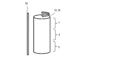
- the roll-shaped mold was divided into three parts (1, 2 and 3) shown in FIG. 6, and each region was evaluated.
- mold shown in FIG. 6 was used for SEM observation and the measurement of an electrical resistance.
- the electrical resistance was measured by a four-terminal method using Loresta AP manufactured by Mitsubishi Chemical Corporation.
- a moth-eye mold was produced under the following conditions.
- Anodizing electrolyte Succinic acid, 0.025 mol / L, 5 ° C
- Etching solution phosphoric acid, 1 mol / L, 30 ° C.
- Anodization time 39 seconds
- Etching time 16 minutes 40 seconds
- the anodic oxidation process was performed 7 times and the etching process was performed 6 times alternately. The last is an anodic oxidation process.
- FIG. 7 shows a graph of the spectral reflectance of the aluminum layer. Although it has a high reflectance in the wavelength range of 400 nm to 700 nm, the reflectance of the roll-shaped part 2 (see FIG. 6) is less than 80%.
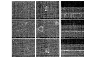
- FIG. 8 shows an SEM image of the aluminum layer on the glass substrate. Corresponding to the part 1, part 2 and part 3 of the roll mold in order from the top. The left end shows a surface SEM image (10,000 times), the center shows a surface SEM image (50000 times), and the right end shows a cross-sectional SEM image (30000 times).
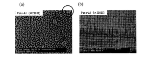
- FIG. 9A and 9B show SEM images (20,000 times) of the porous alumina layer formed from the aluminum layer.
- FIG. 9A shows the SEM image of the surface
- FIG. 9B shows the SEM image of the cross section.
- a peculiar structure is formed in the fine recesses of the porous alumina layer (indicated by ⁇ ). This peculiar structure is considered to be caused by abnormal particles present in the aluminum layer.
- the depth of the fine recessed part which this porous alumina layer has was about 390 nm.
- the resistance to the etching solution was not problematic from the evaluation based on changes in adhesion and electrical resistance (initially and after being immersed in the etching solution for 100 minutes).
- the electrical resistance increased by about 50% when immersed in the etching solution for 100 minutes because the aluminum layer decreased. This was used as a standard for evaluating the etching solution resistance by the electric resistance of the aluminum alloy layer.
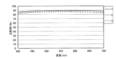
- FIG. 10 shows a graph of spectral reflectance of the Ti-containing aluminum alloy layer. It has a high reflectance exceeding 80% in the wavelength range of 400 nm to 700 nm.
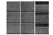
- FIG. 11 shows an SEM image of the Ti-containing aluminum alloy layer on the glass substrate. Corresponding to the part 1, part 2 and part 3 of the roll mold in order from the top. The left end shows a surface SEM image (10,000 times), the center shows a surface SEM image (50000 times), and the right end shows a cross-sectional SEM image (30000 times).
- the Ti-containing aluminum alloy layer is considered to have a higher reflectance than the aluminum layer.
- FIGS. 12A and 12B show SEM images (20,000 times) of the porous alumina layer formed from the Ti-containing aluminum alloy layer.
- 12A shows the SEM image of the surface
- FIG. 12B shows the SEM image of the cross section.
- FIG. 9 (a) the unique structure seen in FIG. 9 (a) is not seen in FIG. 12 (a). This is presumably because abnormal particles do not exist in the Ti-containing aluminum alloy layer, and the Ti-containing aluminum alloy layer has a uniform structure. In addition, the depth of the fine recessed part which this porous alumina layer has was about 330 nm.
- the resistance to the etching solution was not problematic from the evaluation based on changes in adhesion and electrical resistance (initially and after being immersed in the etching solution for 100 minutes).
- the electrical resistance increased by about 80% when immersed in the etching solution for 100 minutes. This is slightly larger than the change in electrical resistance of the aluminum alloy layer, but it can be determined that there is no problem of galvanic corrosion.
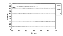
- FIG. 13 shows a graph of spectral reflectance of the Nd-containing aluminum alloy layer. It has a high reflectance exceeding 80% in the wavelength range of 400 nm to 700 nm.
- FIG. 14 shows an SEM image of the Nd-containing aluminum alloy layer on the glass substrate. Corresponding to the part 1, part 2 and part 3 of the roll mold in order from the top. The left end shows a surface SEM image (10,000 times), the center shows a surface SEM image (50000 times), and the right end shows a cross-sectional SEM image (30000 times).
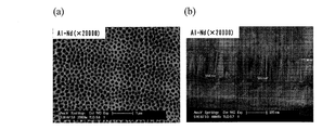
- FIG. 15 (a) and 15 (b) show SEM images (20,000 times) of the porous alumina layer formed from the Nd-containing aluminum alloy layer.
- FIG. 15A shows the SEM image of the surface
- FIG. 15B shows the SEM image of the cross section.
- FIG. 15 (a) does not show the unique structure seen in FIG. 9 (a). This is presumably because no abnormal particles are present in the Nd-containing aluminum alloy layer and the Nd-containing aluminum alloy layer has a uniform structure. In addition, the depth of the fine recessed part which this porous alumina layer has was about 550 nm.
- the resistance to the etching solution was not problematic from the evaluation based on changes in adhesion and electrical resistance (initially and after being immersed in the etching solution for 100 minutes).
- the electrical resistance increased by about 50% when immersed in the etching solution for 100 minutes. This is equivalent to a change in the electric resistance of the aluminum alloy layer, and it can be determined that there is no problem of galvanic corrosion.
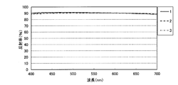
- FIG. 16 shows a graph of spectral reflectance of the Cu-containing aluminum alloy layer. It has a high reflectance exceeding 80% in the wavelength range of 400 nm to 700 nm. It shows a reflectivity close to 90% at most wavelengths.
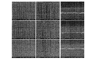
- FIG. 17 shows an SEM image of the Cu-containing aluminum alloy layer on the glass substrate. Corresponding to the part 1, part 2 and part 3 of the roll mold in order from the top. The left end shows a surface SEM image (10,000 times), the center shows a surface SEM image (50000 times), and the right end shows a cross-sectional SEM image (30000 times).
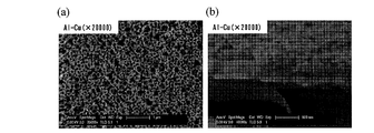
- FIGS. 18A and 18B show SEM images (20,000 times) of the porous alumina layer formed from the Cu-containing aluminum alloy layer.
- 18A shows a SEM image of the surface
- FIG. 18B shows a SEM image of the cross section.
- the porous alumina layer formed from the Cu-containing aluminum alloy layer does not have a form that can be used for manufacturing the antireflection film. This is presumably because the Cu-containing aluminum alloy layer is easily etched.
- the electrical resistance increased by over 600% when immersed in the etching solution for 100 minutes. This is considered to be because when the Cu-containing aluminum alloy layer comes into contact with the etching solution, galvanic corrosion occurs and the Cu-containing aluminum alloy layer dissolves quickly.
- the Ti-containing aluminum alloy 0.5% to 2.0% by weight for the Ti-containing aluminum alloy, 1.0% to 9.9% by weight for the Nd-containing aluminum alloy, and 2.0% for the Zr-containing aluminum alloy.
- the%, Mn-containing aluminum alloy a target of 2 at% (about 4% by mass) is commercially available and can be used immediately industrially.
- the content of the metal element M contained in the aluminum alloy layer is not particularly limited, but preferably does not exceed 10% by mass. When it exceeds 10 mass%, a desired porous alumina layer may not be obtained.
- the example in which the aluminum alloy layer is formed on the organic insulating layer has been described.
- the same effect can be obtained. it can.
- the thermal conductivity of the organic insulating layer is low, and particularly abnormal particles are easily formed, so the effect of using the aluminum alloy layer is remarkable.
- it is interrupted every time an aluminum alloy layer having a thickness of 50 nm is deposited, and 20 layers each having a thickness of 50 nm are formed.
- an aluminum alloy layer 18 having an aluminum alloy layer thickness of about 1 ⁇ m it is easy to form a uniform layer, so that the number of interruptions can be reduced and mass productivity can be improved as compared with the case where an aluminum layer is formed.
- the present invention relates to a method for manufacturing a mold, and in particular, can be widely applied to a method for manufacturing a mold having a porous alumina layer on the surface.
Landscapes
- Chemical & Material Sciences (AREA)
- Engineering & Computer Science (AREA)
- Organic Chemistry (AREA)
- Electrochemistry (AREA)
- Materials Engineering (AREA)
- Metallurgy (AREA)
- Chemical Kinetics & Catalysis (AREA)
- Mechanical Engineering (AREA)
- Physics & Mathematics (AREA)
- General Chemical & Material Sciences (AREA)
- Manufacturing & Machinery (AREA)
- General Physics & Mathematics (AREA)
- Optics & Photonics (AREA)
- Surface Treatment Of Optical Elements (AREA)
- Moulds For Moulding Plastics Or The Like (AREA)
Abstract
Priority Applications (3)
| Application Number | Priority Date | Filing Date | Title |
|---|---|---|---|
| CN201280016614.8A CN103459680B (zh) | 2011-04-01 | 2012-03-29 | 模具的制造方法 |
| US14/008,649 US9512535B2 (en) | 2011-04-01 | 2012-03-29 | Mold production method |
| JP2013508832A JP5615971B2 (ja) | 2011-04-01 | 2012-03-29 | 型の製造方法 |
Applications Claiming Priority (2)
| Application Number | Priority Date | Filing Date | Title |
|---|---|---|---|
| JP2011081590 | 2011-04-01 | ||
| JP2011-081590 | 2011-04-01 |
Publications (1)
| Publication Number | Publication Date |
|---|---|
| WO2012137664A1 true WO2012137664A1 (fr) | 2012-10-11 |
Family
ID=46969065
Family Applications (1)
| Application Number | Title | Priority Date | Filing Date |
|---|---|---|---|
| PCT/JP2012/058394 Ceased WO2012137664A1 (fr) | 2011-04-01 | 2012-03-29 | Procédé de fabrication d'un moule |
Country Status (4)
| Country | Link |
|---|---|
| US (1) | US9512535B2 (fr) |
| JP (1) | JP5615971B2 (fr) |
| CN (1) | CN103459680B (fr) |
| WO (1) | WO2012137664A1 (fr) |
Cited By (5)
| Publication number | Priority date | Publication date | Assignee | Title |
|---|---|---|---|---|
| WO2016084745A1 (fr) * | 2014-11-25 | 2016-06-02 | シャープ株式会社 | Moule, procédé de fabrication de moule, et pellicule antireflet |
| WO2017065090A1 (fr) * | 2015-10-14 | 2017-04-20 | シャープ株式会社 | Procédé de traitement de surface de matériau de base et procédé de production de moule |
| US9914243B2 (en) | 2012-06-06 | 2018-03-13 | Sharp Kabushiki Kaisha | Mold base material, production method for mold base material, mold production method, and mold |
| US20180326624A1 (en) * | 2014-11-12 | 2018-11-15 | Sharp Kabushiki Kaisha | Method for producing mold |
| US11335831B2 (en) | 2017-03-29 | 2022-05-17 | Sharp Kabushiki Kaisha | Optical device case and optical device |
Families Citing this family (7)
| Publication number | Priority date | Publication date | Assignee | Title |
|---|---|---|---|---|
| JP6070720B2 (ja) * | 2012-12-13 | 2017-02-01 | 王子ホールディングス株式会社 | 光学素子作製用金型の製造方法、及び光学素子の製造方法 |
| CN104816410B (zh) * | 2015-03-27 | 2017-03-29 | 豪威光电子科技(上海)有限公司 | 一种镜头模具及其制造方法、及镜头基片的制造方法 |
| CN108699721B (zh) * | 2016-03-02 | 2021-02-19 | 夏普株式会社 | 透镜用模具的制造方法及透镜用模具 |
| CN108360035A (zh) * | 2018-02-07 | 2018-08-03 | 永发(河南)模塑科技发展有限公司 | 一种铝合金材质纸浆成型模具表面阳极氧化处理工艺 |
| JP6467089B1 (ja) | 2018-06-13 | 2019-02-06 | 学校法人東京理科大学 | モスアイ転写型、モスアイ転写型の製造方法及びモスアイ構造の転写方法 |
| JP6948369B2 (ja) * | 2018-11-06 | 2021-10-13 | 学校法人東京理科大学 | モスアイ転写型及びモスアイ転写型の製造方法 |
| CN114645304B (zh) * | 2022-03-30 | 2025-07-25 | 肇庆东弘铝业有限公司 | 一种铝合金型材表面木纹图案成型方法及铝合金型材 |
Citations (4)
| Publication number | Priority date | Publication date | Assignee | Title |
|---|---|---|---|---|
| JP2005232487A (ja) * | 2004-02-17 | 2005-09-02 | Kanagawa Acad Of Sci & Technol | 陽極酸化ポーラスアルミナおよびその製造方法 |
| JP2009037706A (ja) * | 2007-08-02 | 2009-02-19 | Canon Inc | 構造体及びその製造方法 |
| JP2010090430A (ja) * | 2008-10-07 | 2010-04-22 | Fuji Electric Device Technology Co Ltd | アルミニウム合金形成基板及びその製造方法 |
| WO2011105206A1 (fr) * | 2010-02-24 | 2011-09-01 | シャープ株式会社 | Outil, procédé de production d'outil et production d'un film antireflet |
Family Cites Families (12)
| Publication number | Priority date | Publication date | Assignee | Title |
|---|---|---|---|---|
| DE19708776C1 (de) | 1997-03-04 | 1998-06-18 | Fraunhofer Ges Forschung | Entspiegelungsschicht sowie Verfahren zur Herstellung derselben |
| US7066234B2 (en) * | 2001-04-25 | 2006-06-27 | Alcove Surfaces Gmbh | Stamping tool, casting mold and methods for structuring a surface of a work piece |
| DE10020877C1 (de) | 2000-04-28 | 2001-10-25 | Alcove Surfaces Gmbh | Prägewerkzeug, Verfahren zum Herstellen desselben, Verfahren zur Strukturierung einer Oberfläche eines Werkstücks und Verwendung einer anodisch oxidierten Oberflächenschicht |
| JP4406553B2 (ja) | 2003-11-21 | 2010-01-27 | 財団法人神奈川科学技術アカデミー | 反射防止膜の製造方法 |
| KR100893251B1 (ko) * | 2004-12-03 | 2009-04-17 | 샤프 가부시키가이샤 | 반사 방지재, 광학 소자, 및 표시 장치 및 스탬퍼의 제조방법 및 스탬퍼를 이용한 반사 방지재의 제조 방법 |
| CN102016651B (zh) * | 2008-06-06 | 2013-05-22 | 夏普株式会社 | 防反射膜和具备防反射膜的光学元件、压模和压模的制造方法以及防反射膜的制造方法 |
| DE202008013908U1 (de) | 2008-10-17 | 2009-01-08 | Terex-Demag Gmbh | Abstützeinrichtung |
| JP5511313B2 (ja) * | 2008-11-07 | 2014-06-04 | キヤノン株式会社 | 光学素子成形用金型、光学素子成形用金型の製造方法、光学素子、および光学素子の製造方法 |
| BRPI0906259A2 (pt) | 2008-12-26 | 2018-12-26 | Sharp Kk | método de fabricação de um molde e método de produção de um filme antirreflexão usando o molde. |
| RU2482221C1 (ru) * | 2009-04-09 | 2013-05-20 | Шарп Кабусики Кайся | Форма и способ ее изготовления |
| WO2010125795A1 (fr) * | 2009-04-30 | 2010-11-04 | シャープ株式会社 | Moule et procédé de fabrication de celui-ci |
| CN102859048B (zh) * | 2010-04-28 | 2015-07-29 | 夏普株式会社 | 模具和模具的制造方法 |
-
2012
- 2012-03-29 JP JP2013508832A patent/JP5615971B2/ja not_active Expired - Fee Related
- 2012-03-29 WO PCT/JP2012/058394 patent/WO2012137664A1/fr not_active Ceased
- 2012-03-29 US US14/008,649 patent/US9512535B2/en active Active
- 2012-03-29 CN CN201280016614.8A patent/CN103459680B/zh not_active Expired - Fee Related
Patent Citations (4)
| Publication number | Priority date | Publication date | Assignee | Title |
|---|---|---|---|---|
| JP2005232487A (ja) * | 2004-02-17 | 2005-09-02 | Kanagawa Acad Of Sci & Technol | 陽極酸化ポーラスアルミナおよびその製造方法 |
| JP2009037706A (ja) * | 2007-08-02 | 2009-02-19 | Canon Inc | 構造体及びその製造方法 |
| JP2010090430A (ja) * | 2008-10-07 | 2010-04-22 | Fuji Electric Device Technology Co Ltd | アルミニウム合金形成基板及びその製造方法 |
| WO2011105206A1 (fr) * | 2010-02-24 | 2011-09-01 | シャープ株式会社 | Outil, procédé de production d'outil et production d'un film antireflet |
Cited By (7)
| Publication number | Priority date | Publication date | Assignee | Title |
|---|---|---|---|---|
| US9914243B2 (en) | 2012-06-06 | 2018-03-13 | Sharp Kabushiki Kaisha | Mold base material, production method for mold base material, mold production method, and mold |
| US20180326624A1 (en) * | 2014-11-12 | 2018-11-15 | Sharp Kabushiki Kaisha | Method for producing mold |
| US10675788B2 (en) * | 2014-11-12 | 2020-06-09 | Sharp Kabushiki Kaisha | Method for producing mold |
| WO2016084745A1 (fr) * | 2014-11-25 | 2016-06-02 | シャープ株式会社 | Moule, procédé de fabrication de moule, et pellicule antireflet |
| JPWO2016084745A1 (ja) * | 2014-11-25 | 2017-09-07 | シャープ株式会社 | 型および型の製造方法ならびに反射防止膜 |
| WO2017065090A1 (fr) * | 2015-10-14 | 2017-04-20 | シャープ株式会社 | Procédé de traitement de surface de matériau de base et procédé de production de moule |
| US11335831B2 (en) | 2017-03-29 | 2022-05-17 | Sharp Kabushiki Kaisha | Optical device case and optical device |
Also Published As
| Publication number | Publication date |
|---|---|
| US20140197036A1 (en) | 2014-07-17 |
| CN103459680B (zh) | 2016-06-15 |
| US9512535B2 (en) | 2016-12-06 |
| CN103459680A (zh) | 2013-12-18 |
| JP5615971B2 (ja) | 2014-10-29 |
| JPWO2012137664A1 (ja) | 2014-07-28 |
Similar Documents
| Publication | Publication Date | Title |
|---|---|---|
| JP5615971B2 (ja) | 型の製造方法 | |
| JP5797334B2 (ja) | 型基材、型基材の製造方法、型の製造方法および型 | |
| JP5027347B2 (ja) | 型および型の製造方法 | |
| JP5027346B2 (ja) | 型および型の製造方法ならびに反射防止膜の製造方法 | |
| JP4648995B2 (ja) | 型およびその製造方法 | |
| JP4916597B2 (ja) | 型および型の製造方法ならびに反射防止膜 | |
| WO2010125795A1 (fr) | Moule et procédé de fabrication de celui-ci | |
| JPWO2010073636A1 (ja) | 型の製造方法および型を用いた反射防止膜の製造方法 | |
| JP6458051B2 (ja) | 型および型の製造方法ならびに反射防止膜 | |
| JP5833763B2 (ja) | 型の製造方法 |
Legal Events
| Date | Code | Title | Description |
|---|---|---|---|
| 121 | Ep: the epo has been informed by wipo that ep was designated in this application |
Ref document number: 12767746 Country of ref document: EP Kind code of ref document: A1 |
|
| ENP | Entry into the national phase |
Ref document number: 2013508832 Country of ref document: JP Kind code of ref document: A |
|
| WWE | Wipo information: entry into national phase |
Ref document number: 14008649 Country of ref document: US |
|
| NENP | Non-entry into the national phase |
Ref country code: DE |
|
| 122 | Ep: pct application non-entry in european phase |
Ref document number: 12767746 Country of ref document: EP Kind code of ref document: A1 |