WO2012137791A1 - Dispositif d'affichage, son procédé d'attaque, et dispositif électronique - Google Patents
Dispositif d'affichage, son procédé d'attaque, et dispositif électronique Download PDFInfo
- Publication number
- WO2012137791A1 WO2012137791A1 PCT/JP2012/059118 JP2012059118W WO2012137791A1 WO 2012137791 A1 WO2012137791 A1 WO 2012137791A1 JP 2012059118 W JP2012059118 W JP 2012059118W WO 2012137791 A1 WO2012137791 A1 WO 2012137791A1
- Authority
- WO
- WIPO (PCT)
- Prior art keywords
- period
- scanning
- luminance
- display device
- control signal
- Prior art date
- Legal status (The legal status is an assumption and is not a legal conclusion. Google has not performed a legal analysis and makes no representation as to the accuracy of the status listed.)
- Ceased
Links
Images


Classifications
-
- G—PHYSICS
- G09—EDUCATION; CRYPTOGRAPHY; DISPLAY; ADVERTISING; SEALS
- G09G—ARRANGEMENTS OR CIRCUITS FOR CONTROL OF INDICATING DEVICES USING STATIC MEANS TO PRESENT VARIABLE INFORMATION
- G09G3/00—Control arrangements or circuits, of interest only in connection with visual indicators other than cathode-ray tubes
- G09G3/20—Control arrangements or circuits, of interest only in connection with visual indicators other than cathode-ray tubes for presentation of an assembly of a number of characters, e.g. a page, by composing the assembly by combination of individual elements arranged in a matrix no fixed position being assigned to or needed to be assigned to the individual characters or partial characters
- G09G3/34—Control arrangements or circuits, of interest only in connection with visual indicators other than cathode-ray tubes for presentation of an assembly of a number of characters, e.g. a page, by composing the assembly by combination of individual elements arranged in a matrix no fixed position being assigned to or needed to be assigned to the individual characters or partial characters by control of light from an independent source
- G09G3/3406—Control of illumination source
- G09G3/342—Control of illumination source using several illumination sources separately controlled corresponding to different display panel areas, e.g. along one dimension such as lines
- G09G3/3426—Control of illumination source using several illumination sources separately controlled corresponding to different display panel areas, e.g. along one dimension such as lines the different display panel areas being distributed in two dimensions, e.g. matrix
-
- G—PHYSICS
- G02—OPTICS
- G02F—OPTICAL DEVICES OR ARRANGEMENTS FOR THE CONTROL OF LIGHT BY MODIFICATION OF THE OPTICAL PROPERTIES OF THE MEDIA OF THE ELEMENTS INVOLVED THEREIN; NON-LINEAR OPTICS; FREQUENCY-CHANGING OF LIGHT; OPTICAL LOGIC ELEMENTS; OPTICAL ANALOGUE/DIGITAL CONVERTERS
- G02F1/00—Devices or arrangements for the control of the intensity, colour, phase, polarisation or direction of light arriving from an independent light source, e.g. switching, gating or modulating; Non-linear optics
- G02F1/01—Devices or arrangements for the control of the intensity, colour, phase, polarisation or direction of light arriving from an independent light source, e.g. switching, gating or modulating; Non-linear optics for the control of the intensity, phase, polarisation or colour
- G02F1/13—Devices or arrangements for the control of the intensity, colour, phase, polarisation or direction of light arriving from an independent light source, e.g. switching, gating or modulating; Non-linear optics for the control of the intensity, phase, polarisation or colour based on liquid crystals, e.g. single liquid crystal display cells
- G02F1/133—Constructional arrangements; Operation of liquid crystal cells; Circuit arrangements
-
- G—PHYSICS
- G09—EDUCATION; CRYPTOGRAPHY; DISPLAY; ADVERTISING; SEALS
- G09G—ARRANGEMENTS OR CIRCUITS FOR CONTROL OF INDICATING DEVICES USING STATIC MEANS TO PRESENT VARIABLE INFORMATION
- G09G3/00—Control arrangements or circuits, of interest only in connection with visual indicators other than cathode-ray tubes
- G09G3/20—Control arrangements or circuits, of interest only in connection with visual indicators other than cathode-ray tubes for presentation of an assembly of a number of characters, e.g. a page, by composing the assembly by combination of individual elements arranged in a matrix no fixed position being assigned to or needed to be assigned to the individual characters or partial characters
- G09G3/34—Control arrangements or circuits, of interest only in connection with visual indicators other than cathode-ray tubes for presentation of an assembly of a number of characters, e.g. a page, by composing the assembly by combination of individual elements arranged in a matrix no fixed position being assigned to or needed to be assigned to the individual characters or partial characters by control of light from an independent source
- G09G3/3406—Control of illumination source
-
- G—PHYSICS
- G09—EDUCATION; CRYPTOGRAPHY; DISPLAY; ADVERTISING; SEALS
- G09G—ARRANGEMENTS OR CIRCUITS FOR CONTROL OF INDICATING DEVICES USING STATIC MEANS TO PRESENT VARIABLE INFORMATION
- G09G3/00—Control arrangements or circuits, of interest only in connection with visual indicators other than cathode-ray tubes
- G09G3/20—Control arrangements or circuits, of interest only in connection with visual indicators other than cathode-ray tubes for presentation of an assembly of a number of characters, e.g. a page, by composing the assembly by combination of individual elements arranged in a matrix no fixed position being assigned to or needed to be assigned to the individual characters or partial characters
- G09G3/34—Control arrangements or circuits, of interest only in connection with visual indicators other than cathode-ray tubes for presentation of an assembly of a number of characters, e.g. a page, by composing the assembly by combination of individual elements arranged in a matrix no fixed position being assigned to or needed to be assigned to the individual characters or partial characters by control of light from an independent source
- G09G3/36—Control arrangements or circuits, of interest only in connection with visual indicators other than cathode-ray tubes for presentation of an assembly of a number of characters, e.g. a page, by composing the assembly by combination of individual elements arranged in a matrix no fixed position being assigned to or needed to be assigned to the individual characters or partial characters by control of light from an independent source using liquid crystals
- G09G3/3611—Control of matrices with row and column drivers
- G09G3/3648—Control of matrices with row and column drivers using an active matrix
-
- G—PHYSICS
- G09—EDUCATION; CRYPTOGRAPHY; DISPLAY; ADVERTISING; SEALS
- G09G—ARRANGEMENTS OR CIRCUITS FOR CONTROL OF INDICATING DEVICES USING STATIC MEANS TO PRESENT VARIABLE INFORMATION
- G09G3/00—Control arrangements or circuits, of interest only in connection with visual indicators other than cathode-ray tubes
- G09G3/20—Control arrangements or circuits, of interest only in connection with visual indicators other than cathode-ray tubes for presentation of an assembly of a number of characters, e.g. a page, by composing the assembly by combination of individual elements arranged in a matrix no fixed position being assigned to or needed to be assigned to the individual characters or partial characters
- G09G3/34—Control arrangements or circuits, of interest only in connection with visual indicators other than cathode-ray tubes for presentation of an assembly of a number of characters, e.g. a page, by composing the assembly by combination of individual elements arranged in a matrix no fixed position being assigned to or needed to be assigned to the individual characters or partial characters by control of light from an independent source
- G09G3/36—Control arrangements or circuits, of interest only in connection with visual indicators other than cathode-ray tubes for presentation of an assembly of a number of characters, e.g. a page, by composing the assembly by combination of individual elements arranged in a matrix no fixed position being assigned to or needed to be assigned to the individual characters or partial characters by control of light from an independent source using liquid crystals
- G09G3/3611—Control of matrices with row and column drivers
- G09G3/3674—Details of drivers for scan electrodes
-
- G—PHYSICS
- G09—EDUCATION; CRYPTOGRAPHY; DISPLAY; ADVERTISING; SEALS
- G09G—ARRANGEMENTS OR CIRCUITS FOR CONTROL OF INDICATING DEVICES USING STATIC MEANS TO PRESENT VARIABLE INFORMATION
- G09G2310/00—Command of the display device
- G09G2310/08—Details of timing specific for flat panels, other than clock recovery
-
- G—PHYSICS
- G09—EDUCATION; CRYPTOGRAPHY; DISPLAY; ADVERTISING; SEALS
- G09G—ARRANGEMENTS OR CIRCUITS FOR CONTROL OF INDICATING DEVICES USING STATIC MEANS TO PRESENT VARIABLE INFORMATION
- G09G2320/00—Control of display operating conditions
- G09G2320/02—Improving the quality of display appearance
- G09G2320/0271—Adjustment of the gradation levels within the range of the gradation scale, e.g. by redistribution or clipping
-
- G—PHYSICS
- G09—EDUCATION; CRYPTOGRAPHY; DISPLAY; ADVERTISING; SEALS
- G09G—ARRANGEMENTS OR CIRCUITS FOR CONTROL OF INDICATING DEVICES USING STATIC MEANS TO PRESENT VARIABLE INFORMATION
- G09G2320/00—Control of display operating conditions
- G09G2320/06—Adjustment of display parameters
- G09G2320/0626—Adjustment of display parameters for control of overall brightness
- G09G2320/064—Adjustment of display parameters for control of overall brightness by time modulation of the brightness of the illumination source
-
- G—PHYSICS
- G09—EDUCATION; CRYPTOGRAPHY; DISPLAY; ADVERTISING; SEALS
- G09G—ARRANGEMENTS OR CIRCUITS FOR CONTROL OF INDICATING DEVICES USING STATIC MEANS TO PRESENT VARIABLE INFORMATION
- G09G2320/00—Control of display operating conditions
- G09G2320/06—Adjustment of display parameters
- G09G2320/0626—Adjustment of display parameters for control of overall brightness
- G09G2320/0646—Modulation of illumination source brightness and image signal correlated to each other
-
- G—PHYSICS
- G09—EDUCATION; CRYPTOGRAPHY; DISPLAY; ADVERTISING; SEALS
- G09G—ARRANGEMENTS OR CIRCUITS FOR CONTROL OF INDICATING DEVICES USING STATIC MEANS TO PRESENT VARIABLE INFORMATION
- G09G2330/00—Aspects of power supply; Aspects of display protection and defect management
- G09G2330/02—Details of power systems and of start or stop of display operation
- G09G2330/021—Power management, e.g. power saving
-
- G—PHYSICS
- G09—EDUCATION; CRYPTOGRAPHY; DISPLAY; ADVERTISING; SEALS
- G09G—ARRANGEMENTS OR CIRCUITS FOR CONTROL OF INDICATING DEVICES USING STATIC MEANS TO PRESENT VARIABLE INFORMATION
- G09G2340/00—Aspects of display data processing
- G09G2340/04—Changes in size, position or resolution of an image
- G09G2340/0407—Resolution change, inclusive of the use of different resolutions for different screen areas
- G09G2340/0435—Change or adaptation of the frame rate of the video stream
-
- G—PHYSICS
- G09—EDUCATION; CRYPTOGRAPHY; DISPLAY; ADVERTISING; SEALS
- G09G—ARRANGEMENTS OR CIRCUITS FOR CONTROL OF INDICATING DEVICES USING STATIC MEANS TO PRESENT VARIABLE INFORMATION
- G09G2360/00—Aspects of the architecture of display systems
- G09G2360/14—Detecting light within display terminals, e.g. using a single or a plurality of photosensors
- G09G2360/144—Detecting light within display terminals, e.g. using a single or a plurality of photosensors the light being ambient light
Definitions
- the present invention relates to a display device that displays an image or a moving image, a driving method thereof, and an electronic device including the display device.
- a method of reducing power consumption by stopping (intermittent driving) peripheral circuits such as a control circuit and a drive circuit of a display device is known.
- Patent Document 1 discloses a driving method of a display device that realizes low power consumption by providing a pause period longer than a scanning period for scanning the screen once.
- BL control a method of controlling the brightness of a backlight in accordance with the detection result of the intensity of external light to reduce power consumption
- Patent Document 2 discloses a sleep mode having a frequency that is lower than a normal operation clock frequency and does not flicker with respect to a driving circuit of a liquid crystal display device while stopping the operation of a CPU (Central Process Unit). By providing a clock, display flicker is suppressed while reducing power consumption.
- a CPU Central Process Unit
- Japanese Patent Publication Japanese Patent Laid-Open No. 2001-31253 (Publication Date: November 09, 2001)”
- Japanese Patent Publication Japanese Patent Laid-Open No. 2000-347762 (Publication Date: December 15, 2000)”
- Patent Documents 1 and 2 have the following problems.
- the present invention has been made in view of the above-described conventional problems, and an object of the present invention is to provide a display device and the like that can suppress deterioration of display quality during a pause period while reducing power consumption.
- a display device of the present invention includes a scanning line driving circuit that sequentially selects each of a plurality of scanning signal lines on a screen including a plurality of pixels arranged in a matrix, and a selected scanning.
- a signal line driving circuit for sequentially supplying data signals via data signal lines corresponding to each of a plurality of pixels connected to the signal lines, and a scanning period for scanning one screen, all scanning signal lines are in a non-scanning state.
- a drive control unit that drives the scanning line drive circuit and the signal line drive circuit with a pause period, a detection data acquisition unit that acquires detection data of the intensity of external light, and the detection at least in the pause period
- a luminance control signal output unit that outputs a luminance control signal for adjusting the luminance of the light applied to the screen according to the detection data acquired by the data acquisition unit.
- the display device driving method of the present invention includes a scanning line driving circuit that sequentially selects each of a plurality of scanning signal lines on a screen composed of a plurality of pixels arranged in a matrix.
- a signal line driving circuit that sequentially supplies data signals via data signal lines corresponding to each of a plurality of pixels connected to a selected scanning signal line, and a method for driving a display device.
- a driving control step for driving the scanning line driving circuit and the signal line driving circuit by providing a pause period in which all the scanning signal lines are in a non-scanning state, and a detection data for the intensity of external light.
- a brightness for adjusting the brightness of the light applied to the screen according to the detection data acquired in the detection data acquisition process at least in the pause period Characterized in that it comprises a brightness control signal output step of outputting a control signal.
- the scan line drive circuit and the signal are provided by providing a pause period in which all the scan signal lines are in a non-scan state after the scan period for scanning one screen.
- the line drive circuit is driven.
- luminance control signal control for adjusting the luminance of the light applied to the screen according to the detected data is output.
- luminance value control it is possible to adjust the luminance of light applied to the screen at least during the rest period.
- the luminance value control may be stopped at least during the idle period, as in the case where the technique of Patent Document 1 and the luminance value control are simply combined. Therefore, it is possible to suppress the occurrence of problems such as display flickering due to luminance value control not being performed during the pause period.
- an electronic device of the present invention includes a scanning line driving circuit that sequentially selects each of a plurality of scanning signal lines on a screen composed of a plurality of pixels arranged in a matrix.
- a signal line driving circuit that sequentially supplies data signals via data signal lines corresponding to each of a plurality of pixels connected to the scanning signal lines, and a scanning period for scanning one screen, all scanning signal lines are turned off.
- a drive control unit that drives the scanning line drive circuit and the signal line drive circuit by providing a pause period for scanning, a detection data acquisition unit that acquires detection data of the intensity of external light, and at least the pause period, A luminance control signal output unit that outputs a luminance control signal for adjusting the luminance of light applied to the screen according to the detection data acquired by the detection data acquisition unit; And a luminance detection signal output from the luminance control signal output unit of the display device, and irradiates the screen according to the acquired luminance control signal.
- a light irradiating unit that adjusts the luminance of the light.
- the light detection unit outputs detection data of the intensity of external light.
- the light irradiation unit acquires a luminance control signal output from the luminance control signal output unit of the display device, and adjusts the luminance of light applied to the screen according to the acquired luminance control signal.
- the display device of the present invention is connected to the scanning line driving circuit that sequentially selects each of the plurality of scanning signal lines on the screen composed of the plurality of pixels arranged in a matrix, and the selected scanning signal line.
- a signal line driving circuit that sequentially supplies data signals via data signal lines corresponding to each of a plurality of pixels, and a rest period in which all scanning signal lines are in a non-scanning state following a scanning period for scanning one screen
- a drive control unit that drives the scanning line drive circuit and the signal line drive circuit, a detection data acquisition unit that acquires detection data of the intensity of external light, and at least in the pause period, the detection data acquisition unit
- a luminance control signal output unit that outputs a luminance control signal for adjusting the luminance of the light applied to the screen according to the acquired detection data.
- the driving method of the display device of the present invention provides the above-described scanning line driving circuit and the above-described scanning line by providing a rest period in which all scanning signal lines are in a non-scanning state following the scanning period for scanning one screen.
- a luminance control signal output step of outputting a luminance control signal for adjusting the luminance of the light to be irradiated.
- the electronic apparatus of the present invention includes the display device, the light detection unit that outputs detection data of the intensity of external light, and the luminance control signal output from the luminance control signal output unit of the display device. And a light irradiating unit that adjusts the luminance of the light applied to the screen in accordance with the acquired luminance control signal.
- FIG. 1 is a block diagram illustrating an overall configuration of a display system according to an embodiment of the present invention. It is a block diagram which shows the principal part structure of the said display system. It is a block diagram which shows the whole structure of the display system which is other embodiment of this invention. It is a block diagram which shows the principal part structure of the said display system.
- FIG. 6 is a timing chart showing the states of the W_Enable signal, the operation state of each component of the display device, the intensity of external light incident on the screen (display panel), the duty ratio of the PWM signal, and the backlight luminance in the display system. Yes, (a) shows the state when the intensity of external light is high, and (b) shows the state when the intensity of external light is low.
- the state when the intensity of external light gradually increases is shown, and (b) shows the state when the intensity of external light gradually decreases.
- the W_Enable signal, the operating state of each component of the display device, and the intensity of external light incident on the screen when a new scanning period is interrupted in the dimming period in which the duty ratio of the PWM signal is gradually increased 4 is a timing chart showing states of PWM signal duty ratio and backlight luminance.
- the power consumption characteristics of a certain display device are shown in a table.
- FIG. 10 is a graph showing the power consumption characteristics shown in FIG. 9.
- FIGS. 1 to 10 An embodiment of the present invention will be described with reference to FIGS. 1 to 10 as follows. Descriptions of configurations other than those described in the following specific items may be omitted as necessary. However, in the case where they are described in other items, the configurations are the same. For convenience of explanation, members having the same functions as those shown in each item are given the same reference numerals, and the explanation thereof is omitted as appropriate.
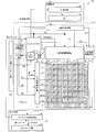
- FIG. 1 is a block diagram showing the overall configuration of the display system 100.
- the display system 100 includes a display device 1, a system-side control unit 30 a, a sensor unit (light detection unit) 40, and a light irradiation unit 50.
- the system-side control unit 30a transmits a horizontal synchronization signal (Hsync signal), a vertical synchronization signal (Vsync signal; arrow B), and an input clock signal (input) to the timing controller 10 as an input video signal (arrow A) and an input video synchronization signal.
- the dot clock signal DCK is output.
- an active matrix liquid crystal display device will be described as an example of the display device 1.
- the present invention is not limited to this, and can also be applied to an EL (electroluminescence) display device that uses a TFT element for addressing.
- the display device 1 can be mounted on a mobile phone, a pocket game machine, a PDA (personal digital assistants), a mobile TV, a remote control, a notebook personal computer, and other mobile terminals. These portable devices are often driven by a battery, and it becomes easy to drive for a long time by installing the display device 1 that can suppress deterioration of display quality while reducing power consumption.
- the display device 1 includes a display panel (screen) 2, a scanning line drive circuit 4, a signal line drive circuit 6, a common electrode drive circuit 8, a timing controller (drive control unit) 10, and a power supply generation circuit 14.
- the display panel 2 selects N scanning signal lines G (n) (gate lines; n is an integer, 0 ⁇ n ⁇ ) for selecting and scanning a screen composed of a plurality of pixels arranged in a matrix in a line-sequential manner.
- N and N are natural numbers).
- M data signal lines S (i) source line; i is an integer, 0 ⁇ i ⁇ M, M is M) that supplies a data signal to a row of pixels included in (connected to) the selected gate line. Natural number).
- the scanning signal line G (n) and the data signal line S (i) are orthogonal to each other.
- G (n) shown in FIG. 1 represents the nth scanning signal line.
- G (1), G (2), and G (3) represent the first, second, and third scanning signal lines, respectively.
- S (i) represents the i-th data signal line.
- S (1), S (2), and S (3) represent the first, second, and third data signal lines, respectively.
- Each pixel in the display panel 2 is provided with a TFT, and the drain electrode of the TFT is connected to the pixel electrode. Has been.
- the scanning line driving circuit 4 scans each scanning signal line G (n) line-sequentially from the top to the bottom of the screen. At that time, a rectangular wave (scanning signal) for turning on a switching element (TFT) provided in the pixel and connected to the pixel electrode is output to each scanning signal line G (n). Thereby, the pixels for one row in the screen are selected.
- a rectangular wave scanning signal
- TFT switching element
- Signal line driving circuit 6 Based on the video signal (arrow E) input from the memory 16, the signal line driving circuit 6 calculates the value of the voltage to be output to each pixel for the selected row, and uses the voltage of that value as the data. Output to the signal line (i). As a result, image data (data signal) is supplied to each pixel on the selected scanning signal line G (n).
- the display device 1 further includes a common electrode (not shown) for each pixel in the screen.
- the common electrode driving circuit 8 drives the common electrode by outputting a predetermined common voltage to the common electrode based on the polarity inversion signal (arrow G) input from the timing controller 10.
- the timing controller 10 has a built-in memory 16, and the memory 16 has a function of recording an input video signal (arrow A) input from the system-side control unit 30a.
- the display device 1 is described as having a configuration including the memory 16, but the display device 1 is not necessarily provided with the memory 16.
- the memory 16 is described as being built in the timing controller 10, but the memory 16 and the timing controller 10 may be provided separately.
- the timing controller 10 receives a horizontal synchronization signal (Hsync signal), a vertical synchronization signal (Vsync signal), and the dot clock signal DCK (arrow B) as input video synchronization signals. Based on the input video synchronization signal and the dot clock signal DCK, the timing controller 10 uses a horizontal synchronization system control signal (gate clock signal GCK, etc.) and a video synchronization signal as a reference for each circuit to operate in synchronization.
- a vertical synchronization control signal eg, a gate start pulse signal GSP
- GSP gate start pulse signal
- the memory 16 outputs a video signal (arrow E) based on the recorded input video signal to the signal line drive circuit 6 in accordance with the video synchronization signal and the dot clock signal DCK received by the timing controller 10.
- the timing controller 10 delivers a gate start pulse signal GSP, a gate clock signal GCK, and a gate output enable signal GOE to the scanning line driving circuit 4, and RGB gradation data to the signal line driving circuit 6.
- a source start pulse signal SSP, a source latch strobe signal SLS, and a source clock signal SCK are distributed.
- the video signal stored in the memory 16 is data that is the basis of the data signal.
- the scanning line driving circuit 4 is a scanning signal line driver, and outputs a voltage corresponding to each of the selection period and the non-selection period to each scanning signal line of the display panel 2. Specifically, the scanning line driving circuit 4 starts scanning the display panel 2 in response to the gate start pulse signal GSP received from the timing controller 10 and sequentially applies a selection voltage to each scanning signal line in accordance with the gate clock signal GCK. I will do it.
- the signal line drive circuit 6 is a data signal line driver, outputs a data signal to each data signal line of the display panel 2, and supplies image data to each of the pixels on the selected scanning signal line. Specifically, the signal line drive circuit 6 stores the received gradation data of each pixel in a register (not shown) according to the source clock signal SCK based on the source start pulse signal SSP received from the timing controller 10. The gradation data is written to each data signal line of the display panel 2 in accordance with the next source latch strobe signal SLS.
- the timing controller 10 adjusts the vertical synchronization system control signal (such as the pulse interval of the gate start pulse signal GSP) and the horizontal synchronization system control signal (such as the frequency of the gate clock signal GCK).
- a pause drive control unit 108 that generates a pause drive control signal (hereinafter referred to as a W_Enable signal) is provided.
- the pause drive control unit 108 drives the scanning line drive circuit 4 and the signal line drive circuit 6 by providing a pause period T2 in which all the scanning signal lines are in a non-scanning state following the scanning period T1 for scanning one screen.
- the length of the pause period T2 may be shorter than the scan period T1, but from the viewpoint of reducing power consumption, the length of the pause period T2 is preferably longer than the scan period T1. .
- the pulse interval of the gate start pulse signal GSP is about 16.7 msec when the display frame frequency is a normal 60 Hz.
- the pause drive control unit 108 increases the pulse interval of the gate start pulse signal GSP to 167 msec. Assuming that the scanning period T1 for one screen remains normal, about 9/10 of the above-described pulse interval is a period during which all scanning signal lines are in a non-scanning state. As described above, the pause drive control unit 108 determines that the non-scanning period (all scanning signal lines are not selected) until the gate start pulse signal GSP is input to the scanning line driving circuit 4 again after the scanning period T1 ends. The period during which scanning is performed) may be set to be longer than the scanning period T1.
- one display cycle is the sum of the scan period T1 and the pause period T2.
- the scanning period T1 is set to a time equivalent to a normal 60 Hz
- the scanning period T1 and the non-scanning period may be appropriately set according to the degree of movement in an image to be displayed such as a still image or a moving image, and the pause drive control unit 108 sets a plurality of non-scanning periods according to the content of the image. Can be done.
- the pause period T2 is set as the non-scanning period. If set, the power consumption of the signal line drive circuit 6 that increases in proportion to the supply frequency of the data signal can be easily and sufficiently reduced without sacrificing the display quality.
- the non-scanning period may be set to the long pause period T2 for a display with no movement such as a still image or a display with little movement even with a moving image.
- a short pause period T2 may be set as a non-scanning period. For example, if a non-scanning period that is sufficiently short with respect to a scanning period of 16.7 msec is set, the drive frequency is equivalent to a normal 60 Hz, so that a sufficiently fast moving image can be displayed.
- the non-scanning period is set to a long pause period T2 of 3333 msec, it is possible to reduce the power consumption by rewriting the screen while maintaining the basic display quality for still images and moving images with little movement. it can. That is, the display panel 2 can be used by switching between a moving image display and a low power consumption display. As described above, since the cycle of rewriting the screen can be changed in accordance with the type of display image such as a still image or a moving image, it is possible to achieve optimum low power consumption for each type of display image.
- one vertical period means a period defined based on the Vsync signal
- one horizontal period means the Hsync signal. It means the period specified based on
- the display device 1 has the memory 16 as in the present embodiment and, for example, double-speed display is possible, the display device 1 has a separate clock generation circuit. Is also possible. Therefore, in such a case, the time interval of the clock incorporated in the display device 1 is used regardless of one vertical period and one horizontal period composed of the Vsync signal and the Hsync signal input from the system-side control unit 30a side.
- One vertical period and one horizontal period may be defined.
- the unit of the length of each of the later-described scanning frame, pause frame, and interrupt scanning frame is one vertical period, and is counted as one frame for each vertical period. For example, when the length of the pause frame is 9 vertical periods, the pause frame has a length of 9 frames.
- the scanning line driving circuit 4 starts scanning the display panel 2 in accordance with the horizontal synchronizing signal, the vertical synchronizing signal, and the W_Enable signal received from the timing controller 10, and sequentially selects and scans each scanning signal line G (n). Output a signal.
- the signal line driving circuit 6 receives image data (data signal) based on the video signal input from the memory 16 in accordance with the horizontal synchronization signal and the W_Enable signal received from the timing controller 10, and the data signal lines S ( Write sequentially to i).
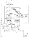
- FIG. 2 is a block diagram illustrating a main configuration of the display system 100.
- the timing controller 10 includes a data analysis unit (detection data acquisition unit) 101, a BL luminance level determination unit 102, a BL luminance dimming period determination unit 103, and a BL luminance setting unit (luminance control signal output unit) 104.
- the data analysis unit 101 sends a sensing command signal (hereinafter referred to as S_Enable signal) to the sensor unit 40 at a predetermined timing.
- S_Enable signal a sensing command signal
- the sensing unit control unit 26 of the sensor unit 40 receives the S_Enable signal, operates the sensing unit 24, and receives detection data (analog) detected by the sensing unit 24.
- the sensing unit control unit 26 performs the following calculation processes (1) to (4) on the detection data (analog) received from the sensing unit 24, and returns the calculation result to the data analysis unit 101.
- a / D (analog / digital) conversion is performed on detection data (analog data) to output detection data (digital data).
- Noise of detection data (digital data) is removed using a 50/60 Hz flicker removal filter.
- the median filter is a filter that arranges the calculation results of (3) (corresponding to each voltage value detected from a PD arranged in a matrix, which will be described later) in ascending order, and extracts the median (median).
- the data analysis unit 101 receives the above calculation result from the sensing unit control unit 26 (detection data acquisition step), and a plurality of levels of illuminance levels (output standards; And 16 levels on the UP side and 16 levels on the DOWN side) and the determined brightness level category is notified to the BL brightness level determination unit 102.
- the BL luminance level determination unit 102 determines a BL luminance setting value (luminance setting value) based on the illuminance level classification notified from the data analysis unit 101.
- the determined BL brightness setting value is passed to the BL brightness dimming period determination unit 103.
- the intensity of external light (detection data) and the BL brightness setting value are associated with each other in advance, and the BL brightness level determination unit 102 determines the BL brightness setting value based on this correspondence.
- the above-described plurality of levels of illuminance levels are associated such that the illuminance level increases (decreases) as the intensity of external light increases (decreases).
- the BL luminance dimming period determining unit 103 determines the length (how many frames) of the dimming period Td during which BL control is performed. In the present embodiment, a period from 1 frame to a maximum of 256 frames (256 steps) can be set. However, the dimming period Td is not limited to the above-described 256 stages, and may exceed 256 stages (256 frames).
- the BL brightness setting unit 104 may determine a BL brightness setting value for each vertical synchronization period (one frame) included in the dimming period Td in the dimming period Td including at least one frame (output standard).
- the luminance of the backlight light can be adjusted with little flickering on the display.
- the BL luminance setting unit 104 generates a pulse width modulation signal (PWM signal) as a BL control signal from the BL luminance setting value and the dimming period Td received from the BL luminance dimming period determining unit 103, and the light irradiation unit 50 (BL control) Part 36) (luminance control signal output step).
- PWM signal pulse width modulation signal
- the duty ratio (duty ratio) of the PWM signal changes according to the BL brightness setting value. That is, when the BL brightness setting value is large, the duty ratio of the PWM signal is also increased, and when the BL brightness setting value is small, the duty ratio of the PWM signal is also decreased.
- the present invention is not limited to this.
- the backlight becomes brighter when the duty ratio of the PWM signal is smaller, conversely, when the BL luminance setting value is large, the duty ratio of the PWM signal is small and the BL luminance setting value is small. The duty ratio of the PWM signal is increased.
- the PWM signal as the BL control signal (brightness control signal) sent from the BL brightness setting unit 104 to the BL control unit 36, the PWM signal is supplied to the BL control unit 36 with a single lead, and the backlight. Therefore, the configuration of the display system 100/200 becomes simpler.
- the data analysis unit 101 receives the above calculation result from the sensing unit control unit 26, and the value of the received calculation result is a predetermined gradation level classification (output reference; for example, reference gradation level). And 16 levels on the UP side and 16 levels on the DOWN side) and the determined gradation value classification is notified to the gradation setting determination unit 105.
- a predetermined gradation level classification output reference; for example, reference gradation level
- the gradation setting determination unit 105 determines a gradation setting value based on the gradation value classification notified from the data analysis unit 101.
- the determined gradation setting value is transferred to the gradation setting dimming period determination unit 106.
- the intensity (detection data) of the external light is associated with the gradation setting value in advance, and the gradation setting determining unit 105 determines the gradation setting value based on this correspondence. Further, the above-described gradation value divisions in multiple stages are associated with each other so that the gradation value increases (decreases) as the intensity of external light increases (decreases). Thereby, even when the intensity of the external light changes during the suspension period T2, it is possible to determine whether the gradation value of the pixel of the display panel 2 is to be higher or lower, so that the external light during the suspension period can be determined. Image processing according to intensity (hereinafter referred to as “tone value control”) can be performed appropriately. Thereby, deterioration of display quality can be suppressed.
- tone value control image processing according to intensity
- the gradation setting dimming period determination unit 106 determines the length (how many frames) of the dimming period Td, which is a period for performing gradation value control. Note that the dimming period that is the period for performing the BL control and the dimming period that is the period for performing the gradation value control may be set independently, but in the present embodiment, a common dimming period is set. The period is called a dimming period Td.
- the determined dimming period Td is transferred to the gradation setting control unit 107 and the pause drive control unit 108.
- the gradation setting control unit 107 generates a gradation control signal (such as gradation data) from the gradation setting value and the dimming period Td received from the gradation setting dimming period determination unit 106, and determines the video data output timing. Passed to part 109.
- the video data output timing determination unit 109 may temporarily store the received gradation setting value and dimming period Td in the memory 16.
- the pause drive control unit 108 generates a W_Enable signal in which an interrupt scan frame is interrupted within the dimming period Td.
- the gradation setting determination unit 105 may set a gradation control signal for each vertical synchronization period (one frame) included in the dimming period Td in the dimming period Td including at least one vertical synchronization period ( Output standard).
- the gradation value of the pixel of the display panel 2 can be adjusted with almost no flickering on the display.
- the BL luminance dimming period and the gradation setting dimming period may be the same period or different periods.
- the power generation circuit 14 generates Vdd, Vdd2, Vcc, Vgh, and Vgl, which are voltages necessary for the operation of each circuit of the display device 1. Then, Vcc, Vgh, and Vgl are output to the scanning line driving circuit 4, Vdd and Vcc are output to the signal line driving circuit 6, Vcc is output to the timing controller 10, and Vdd 2 is output to the common electrode driving circuit 8.
- the sensor unit 40 includes a sensing unit 24 and a sensing unit control unit 26.
- the sensing unit control unit 26 receives a detection command signal from the timing controller 10, generates a sensing unit drive signal, and outputs the sensing unit drive signal to the sensing unit 24.
- the detection command signal and the sensing unit drive signal are both referred to as “S_Enable signal”.
- the sensing unit control unit 26 performs the above arithmetic processing on the detection data (analog) received from the sensing unit 24 and outputs the calculation result to the timing controller 10.
- the sensing unit 24 includes a single or a plurality of optical sensors (not shown), receives an S_Enable signal from the sensing unit control unit 26, performs a detection operation, and returns detection data (analog) to the sensing unit control unit 26.
- the sensing unit 24 will be described as including a so-called touch sensor in which an optical sensor is built in each pixel. That is, the display panel 2 of the display device 1 has a configuration in which, for example, a photodiode (PD) is incorporated as a photosensor in each pixel. A capacitor is connected to the PD, and the charge amount of the capacitor is changed in accordance with a change in the amount of incident light incident on the PD. Then, the intensity of incident light incident on the PD can be detected by detecting the voltage across the capacitor.
- the external light component incident on the display panel 2 is included in the incident light incident on the PD, and the intensity of the external light incident on the display panel 2 can be detected by analyzing the detection data. It has become.
- the light irradiation unit 50 includes a BL (backlight) 34 and a BL control unit (backlight control unit) 36.
- the BL 34 includes a plurality of LEDs (Light Emitting Diodes), and each LED emits light by a current I supplied from the BL control unit 36 (backlight light is emitted from the BL 34).
- the backlight light emitted from the BL 34 is applied to the display panel 2.
- a BL (backlight) 34 is provided as an example of a light source (light irradiating unit) that irradiates the display panel 2 with light.
- the light source for irradiating the display panel 2 with light is not limited to the backlight, but may be a front light or the like.
- the BL control unit 36 determines the effective value of the current I supplied to each of the plurality of LEDs constituting the BL 34 according to the duty ratio (duty ratio) of the pulse width modulation signal (PWM signal) received from the BL luminance setting unit 104. Is supplied to BL34.
- FIG. 3 is a block diagram showing the overall configuration of the display system 200
- FIG. 4 shows the main configuration of the display system 200.
- the display system 200 of the present embodiment is different from the display system 100 as follows.
- the system-side control unit (drive control unit) 30b sends an S_Enable signal to the sensor unit 40 and receives detection data (calculation result) from the sensor unit 40.
- the system-side control unit 30b passes the received detection data to the timing controller 10.
- the sensing unit control unit 26 passes detection data (analog) received from the sensing unit 24 as it is to the system side control unit 30b, and the system side control unit 30b performs the above arithmetic processing.
- the system-side control unit 30 b receives a BL control signal from the BL brightness setting unit 104 and passes the received BL control signal to the light irradiation unit 50.
- the BL luminance setting unit 104 passes the BL luminance setting value and the dimming period Td received from the BL luminance dimming period determining unit 103 to the system side control unit 30b as they are, and the system side control unit 30b
- the PWM signal may be generated and sent to the light irradiation unit 50.
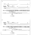
- Example 1 First, an example (Example 1) of main operations of the display systems 100 and 200 will be described with reference to FIGS. 5A and 5B.
- the timing controller 10 provides a scanning period T1 (scanning frame) for scanning one screen and a scanning period driving circuit 4 by providing a pause period T2 (pause frame) in which all scanning signal lines are in a non-scanning state. And the signal line drive circuit 6 is driven (drive control process).
- the power consumption of the scanning line driving circuit 4 that increases in proportion to the supply frequency of the data signal can be easily reduced.
- FIG. 5A shows a state in which the intensity of external light increases as time advances from a certain point in the suspension period T2.
- (a) of FIG. 5 shows a state in which the intensity of external light decreases as time advances from a certain point in the suspension period T2.
- the sensor unit 40 and the light irradiation unit 50 are set to be in an operating state (in operation) at least during the suspension period T2.
- the BL control unit 36 increases the luminance of the backlight light emitted from the BL 34 to the display panel 2 when the intensity of the external light detected by the sensor unit 40 increases ((a) in FIG. 5). ).
- the BL control unit 36 reduces the luminance of the backlight light emitted from the BL 34 to the display panel 2.
- the duty ratio (duty ratio) of the pulse width modulation signal (PMW) is increased (decreased) at an interval of one frame (output reference). Therefore, as shown in FIG. The change changes stepwise unlike the change in the intensity of external light.
- the display systems 100 and 200 perform BL control (and / or gradation value control) at least during the suspension period T2.
- the longer the pause period T2 the higher the effect of reducing power consumption. Therefore, it is preferable to set the pause period T2 to be relatively longer than the scanning period T1. At this time, the probability that the change in the intensity of external light is captured is higher in the pause period T2.
- the BL control (and / or gradation value control) is stopped in the suspension period T2, as in the case where the technique of Patent Document 1 and the BL control (and / or gradation value control) are simply combined. If this is the case, BL control (and / or gradation value control) is not effectively performed, and there is a high possibility that problems such as display flickering will occur.
- the BL control (and at least the idle period T2) (and the BL control (and / or gradation value control) described above and the BL control (and / or gradation value control)) are simply combined. (Or gradation value control) does not stop, so that occurrence of problems such as display flickering due to the absence of BL control (and / or gradation value control) during the suspension period T2 can be suppressed. it can.
- a sleep clock lower than the normal operation clock frequency is given to the drive circuit of the liquid crystal display device in the low power consumption mode.
- the clock frequency used as a reference for gradation value control is also lowered.
- the BL brightness setting unit 104 and / or the gradation setting control unit 107 is configured to display the brightness control signal and / or the rest period T2.
- the gradation control signal is output according to the same output standard as that in the scanning period T1.
- the BL luminance setting value and / or the gradation setting value are set with respect to the intensity of the external light.
- a case where the criteria to be determined are the same can be exemplified.
- the luminance value control (and / or gradation value control) according to the same output standard as the luminance value control (and / or gradation value control) in the scanning period is performed in the pause period. Therefore, for example, unlike the technique described in Patent Document 2, the operation of luminance value control (and / or gradation value control) does not slow down during the pause period. That is, since the same brightness value control (and / or gradation value control) is performed in the scanning period and the rest period, dynamic brightness value control (and / or dynamics) is performed in both the scanning period and the rest period. The function of (tone value control) can be fully exhibited. Therefore, deterioration of display quality can be suppressed.
- Example 2 Next, another example (Example 2) of main operations of the display systems 100 and 200 will be described with reference to FIGS. 6A and 6B.
- This figure shows a case where the dimming period Td for performing the BL control is composed of a plurality of frames.
- the BL control unit 36 gradually adjusts the luminance of the backlight light for each frame included in the dimming period Td in the dimming period Td composed of a plurality of frames.
- the intensity of the external light gradually increases (or gradually decreases), so that the luminance of the backlight light gradually increases ( Or gradually lower).
- the luminance of the backlight light also increases.
- gradually decreasing gradually decreasing, then gradually increasing.
- the display systems 100 and 200 As the number of frames included in the dimming period Td increases, it is possible to perform dynamic BL control following changes in the intensity of external light. Therefore, the luminance of the backlight light can be adjusted with little flickering on the display.
- Example 3 Next, still another example (Example 3) of main operations of the display systems 100 and 200 will be described based on FIGS. 7A, 7B, and 8.
- FIG. 7A, 7B, and 8 Still another example (Example 3) of main operations of the display systems 100 and 200 will be described based on FIGS. 7A, 7B, and 8.
- This figure shows a case where the dimming period Td for performing the BL control is composed of a plurality of frames.
- a new scanning period (interrupt scanning period or interrupt scanning frame) is interrupted in the dimming period Td in order to perform gradation value control in conjunction with BL control in the dimming period Td in which BL control is performed.
- the refresh rate can be increased as compared with the case where no interrupt scanning frame is provided. Therefore, flicker that tends to occur when the refresh rate decreases due to the characteristics of the display panel 2 can be suppressed.
- the interrupt scanning period may be ended at the timing when the dimming period Td ends (the timing at which the output of the BL control signal is stopped) and returned to the idle period.
- the length of the scan frame other than the interrupt scan frame is always T1 regardless of the presence or absence of the interrupt scan frame. Yes, the length of the pause frame is always T2.
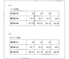
- FIG. 9 is a table showing power consumption characteristics of a certain display device.
- FIG. 10 is a graph showing the power consumption characteristics shown in FIG.
- This power consumption characteristic is that of a 10.8 type liquid crystal display device that employs a TFT using an oxide semiconductor as the TFT of each pixel.
- the power consumption can be reduced as the refresh rate of the display panel is lowered.
- source inversion is set as the polarity inversion method and “60 Hz” is set as the refresh rate.
- the power consumption of the display device is “417.78 mW”.
- the refresh rate is reduced to “30 Hz”.
- the power consumption of the display device is “309.87 mW”, and the power consumption is reduced by “107.91 mW”.
- the polarity inversion method is further changed from “source inversion” to “2H dot inversion” in order to suppress deterioration in display image quality due to the change in the refresh rate.
- the power consumption of the display device is “416.79 mW”, and the power consumption is increased by “106.92 mW”.
- the increase amount reduces the power consumption reduction amount due to the decrease in the refresh rate. It can be seen that it cannot be exceeded.
- a sleep clock lower than the normal operation clock frequency is given to the driving circuit of the liquid crystal display device in the low power consumption mode.
- the clock frequency becomes lower.
- the operation of the brightness value control is also slowed down, and dynamic brightness value control (for example, active adjustment of adjusting the brightness value of the backlight light according to the detection result of the intensity of external light)
- dynamic brightness value control for example, active adjustment of adjusting the brightness value of the backlight light according to the detection result of the intensity of external light
- the function of dynamic luminance value control cannot be fully exhibited, and there is a possibility that problems such as display flickering may occur.
- the luminance control signal output unit may output the luminance control signal in the pause period according to the same output standard as that in the scanning period.
- the luminance value control according to the same output standard as the luminance value control in the scanning period is performed in the pause period. Therefore, for example, unlike the technique described in Patent Document 2, the brightness value control operation does not slow down during the pause period. That is, since the same brightness value control is performed in the scanning period and the rest period, the function of dynamic brightness value control can be sufficiently exhibited in both the scanning period and the rest period. Therefore, deterioration of display quality can be suppressed.
- the output standard is the same
- the time interval for performing the luminance value control is the same
- the standard for determining the luminance of the light with respect to the intensity of the external light is the same Etc.
- the luminance control signal output unit is responsive to a luminance setting value determined based on a correspondence relationship between a predetermined intensity of external light and the luminance of light irradiated on the screen.
- the luminance control signal may be generated.
- the luminance control signal output unit is a period in which the luminance of the light is adjusted, and the vertical synchronization included in the dimming period is a dimming period including at least one vertical synchronization period.
- the luminance control signal may be output every period.
- the luminance of light can be adjusted with almost no flickering on the display.
- the drive control unit may provide a new scanning period within the dimming period.
- the refresh rate can be increased as compared with the case where no new scanning period is provided. Therefore, flicker that tends to occur when the refresh rate decreases due to the characteristics of the screen (display panel) can be suppressed.
- the drive control unit may end the new scanning period and return to the idle period at a timing when the luminance control signal output unit stops outputting the luminance control signal.
- the luminance control signal output unit generates, as the luminance control signal, a pulse width modulation signal in which a duty ratio is adjusted according to the luminance setting value determined based on the correspondence relationship. You may do it.
- the pulse width modulation signal (PWM signal) can be supplied to, for example, the above-described light irradiation unit with a single conductor, and the luminance of the light can be adjusted, so that the configuration of the display device can be simplified.
- the display device of the present invention may be a liquid crystal display device.
- gradation value control a method of controlling the gradation value output to each pixel of the screen according to the detection result of the intensity of external light and reducing the power consumption. (Abbreviated) is also conceivable.
- the display device of the present invention provides a gradation control signal for adjusting the gradation value output to each pixel of the screen according to the detection data acquired by the detection data acquisition unit at least in the new scanning period. May be provided.
- the gradation control signal output unit adjusts the gradation value output to each pixel of the screen according to the detection data acquired by the detection data acquisition unit at least in the new scanning period.
- the display device of the present invention can perform gradation value control at least in a new scanning period.
- the gradation control signal output unit may determine the gradation determined based on a correspondence relationship between a predetermined external light intensity and a gradation value output to each pixel of the screen.
- the gradation control signal may be generated according to the set value.
- the gradation control signal output unit may output the gradation control signal for each vertical synchronization period included in the new scanning period.
- the gradation value output to each pixel of the screen can be adjusted with almost no flickering on the display.
- the output reference may include a reference that makes the time interval for performing the luminance value control in the pause period the same as the time interval in the scanning period.
- a standard for determining the luminance setting value with respect to the intensity of external light during the pause period is the same as a standard for determining the luminance setting value with respect to the intensity of external light during the scanning period. Also good.
- the luminance value control according to the same output standard as the luminance value control in the scanning period is performed in the pause period. Therefore, for example, unlike the technique described in Patent Document 2, the brightness value control operation does not slow down during the pause period. That is, since the same brightness value control is performed in the scanning period and the rest period, the function of dynamic brightness value control can be sufficiently exhibited in both the scanning period and the rest period. Therefore, deterioration of display quality can be suppressed.
- the display device according to the present invention can be widely used as various display devices such as liquid crystal display devices, organic EL display devices, and electronic paper.
- Display device liquid crystal display device
- Display panel screen
- Scanning line drive circuit Signal line drive circuit
- Timing controller drive control unit
- System side control unit drive control unit
- Sensor part light detection part
- Light Irradiation Unit 100, 200 Display System (Display Device)
- Data analysis unit detection data acquisition unit
- BL luminance setting unit luminance control signal output unit
- gradation setting control section gradation control signal output section
Landscapes
- Engineering & Computer Science (AREA)
- Physics & Mathematics (AREA)
- General Physics & Mathematics (AREA)
- Theoretical Computer Science (AREA)
- Computer Hardware Design (AREA)
- Crystallography & Structural Chemistry (AREA)
- Chemical & Material Sciences (AREA)
- Nonlinear Science (AREA)
- Mathematical Physics (AREA)
- Optics & Photonics (AREA)
- Control Of Indicators Other Than Cathode Ray Tubes (AREA)
- Liquid Crystal Display Device Control (AREA)
- Liquid Crystal (AREA)
Abstract
Priority Applications (5)
| Application Number | Priority Date | Filing Date | Title |
|---|---|---|---|
| US14/000,655 US8810615B2 (en) | 2011-04-07 | 2012-04-03 | Display device, drive method thereof, and electronic device |
| KR1020137018101A KR101346925B1 (ko) | 2011-04-07 | 2012-04-03 | 표시 장치, 그 구동 방법 및 전자 기기 |
| CN201280004649.XA CN103282954B (zh) | 2011-04-07 | 2012-04-03 | 显示装置、其驱动方法以及电子设备 |
| JP2013508886A JP5290481B2 (ja) | 2011-04-07 | 2012-04-03 | 表示装置、その駆動方法および電子機器 |
| US14/327,665 US8970645B2 (en) | 2011-04-07 | 2014-07-10 | Display device, drive method thereof, and electronic device |
Applications Claiming Priority (6)
| Application Number | Priority Date | Filing Date | Title |
|---|---|---|---|
| JP2011-085813 | 2011-04-07 | ||
| JP2011085813 | 2011-04-07 | ||
| JP2011177221 | 2011-08-12 | ||
| JP2011-177221 | 2011-08-12 | ||
| JP2011-280500 | 2011-12-21 | ||
| JP2011280500 | 2011-12-21 |
Related Child Applications (2)
| Application Number | Title | Priority Date | Filing Date |
|---|---|---|---|
| US14/000,655 A-371-Of-International US8810615B2 (en) | 2011-04-07 | 2012-04-03 | Display device, drive method thereof, and electronic device |
| US14/327,665 Continuation US8970645B2 (en) | 2011-04-07 | 2014-07-10 | Display device, drive method thereof, and electronic device |
Publications (1)
| Publication Number | Publication Date |
|---|---|
| WO2012137791A1 true WO2012137791A1 (fr) | 2012-10-11 |
Family
ID=46969187
Family Applications (1)
| Application Number | Title | Priority Date | Filing Date |
|---|---|---|---|
| PCT/JP2012/059118 Ceased WO2012137791A1 (fr) | 2011-04-07 | 2012-04-03 | Dispositif d'affichage, son procédé d'attaque, et dispositif électronique |
Country Status (5)
| Country | Link |
|---|---|
| US (2) | US8810615B2 (fr) |
| JP (1) | JP5290481B2 (fr) |
| KR (1) | KR101346925B1 (fr) |
| CN (2) | CN103282954B (fr) |
| WO (1) | WO2012137791A1 (fr) |
Cited By (5)
| Publication number | Priority date | Publication date | Assignee | Title |
|---|---|---|---|---|
| WO2013125458A1 (fr) * | 2012-02-24 | 2013-08-29 | シャープ株式会社 | Dispositif d'affichage, dispositif électronique comprenant ledit dispositif et procédé de commande pour le dispositif d'affichage |
| WO2014080812A1 (fr) * | 2012-11-20 | 2014-05-30 | シャープ株式会社 | Dispositif à cristaux liquides et son procédé de pilotage |
| KR20140067778A (ko) * | 2012-11-27 | 2014-06-05 | 엘지디스플레이 주식회사 | 타이밍 컨트롤러 및 그 구동 방법과 이를 이용한 표시장치 |
| EP2801970A1 (fr) * | 2013-05-10 | 2014-11-12 | LG Display Co., Ltd. | Appareil d'affichage et procédé de commande d'appareil d'affichage avec adaptation de la luminosité du rétroéclairage et de la fréquence des trames |
| JP2018054901A (ja) * | 2016-09-29 | 2018-04-05 | 株式会社半導体エネルギー研究所 | 表示システムおよび電子機器 |
Families Citing this family (19)
| Publication number | Priority date | Publication date | Assignee | Title |
|---|---|---|---|---|
| KR102059561B1 (ko) * | 2013-04-08 | 2019-12-30 | 삼성디스플레이 주식회사 | 유기전계발광 표시장치 및 그의 구동방법 |
| KR102087967B1 (ko) * | 2013-07-30 | 2020-04-16 | 삼성디스플레이 주식회사 | 액정 표시 장치 및 그 구동 방법 |
| CN105518773B (zh) * | 2013-09-05 | 2018-05-29 | 夏普株式会社 | 液晶显示装置 |
| WO2015199049A1 (fr) * | 2014-06-23 | 2015-12-30 | シャープ株式会社 | Dispositif d'affichage et procédé d'affichage |
| JP2016066065A (ja) | 2014-09-05 | 2016-04-28 | 株式会社半導体エネルギー研究所 | 表示装置、および電子機器 |
| CN104267607A (zh) * | 2014-09-10 | 2015-01-07 | 京东方科技集团股份有限公司 | 调节室内光亮度的方法、装置和智能家居控制系统 |
| US9830849B2 (en) | 2015-02-09 | 2017-11-28 | Apple Inc. | Entry controlled inversion imbalance compensation |
| US10311813B2 (en) | 2015-06-05 | 2019-06-04 | Sharp Kabushiki Kaisha | Control device, display device, control method, and storage medium |
| US9728142B2 (en) * | 2015-07-15 | 2017-08-08 | Christie Digital Systems Usa, Inc. | Reduced blur, low flicker display system |
| WO2017033709A1 (fr) * | 2015-08-24 | 2017-03-02 | 三菱電機株式会社 | Dispositif d'affichage à diodes électroluminescentes et procédé permettant de corriger la luminance de ce dernier |
| CN105047144B (zh) * | 2015-09-08 | 2018-01-12 | 武汉华星光电技术有限公司 | 液晶显示装置及其背光控制方法 |
| CN106710506B (zh) * | 2017-01-18 | 2020-07-14 | 京东方科技集团股份有限公司 | 显示面板的驱动方法、驱动电路、显示面板及显示装置 |
| CN107016966B (zh) * | 2017-05-10 | 2019-01-22 | 昆山龙腾光电有限公司 | 背光模组控制系统、控制方法及具有该系统的液晶模组 |
| CN107896308B (zh) * | 2017-10-27 | 2020-08-18 | 天津大学 | 脉冲阵列式仿视网膜图像传感器 |
| CN109754759B (zh) * | 2017-11-08 | 2020-11-06 | 京东方科技集团股份有限公司 | 背光源控制装置、方法及显示装置 |
| CN109254548A (zh) * | 2018-08-30 | 2019-01-22 | 浙江工业大学 | 一种基于stm32f407zet6的木球挥杆速度检测系统 |
| WO2022029830A1 (fr) * | 2020-08-03 | 2022-02-10 | シャープ株式会社 | Dispositif d'affichage et son procédé d'attaque |
| US11915635B2 (en) * | 2022-02-24 | 2024-02-27 | Tcl China Star Optoelectronics Technology Co., Ltd. | Dimming method and device of display panel, storage medium, and terminal equipment |
| DE112023006083T5 (de) * | 2023-03-29 | 2026-01-15 | Boe Technology Group Co., Ltd. | Treiberschaltung, Treiberverfahren, Pixelschaltung, Anzeigefeld und Anzeigevorrichtung |
Citations (7)
| Publication number | Priority date | Publication date | Assignee | Title |
|---|---|---|---|---|
| JPH08286170A (ja) * | 1995-02-16 | 1996-11-01 | Toshiba Corp | 液晶表示装置 |
| JP2001312253A (ja) * | 2000-04-28 | 2001-11-09 | Sharp Corp | 表示装置の駆動方法およびそれを用いた表示装置ならびに携帯機器 |
| JP2007072243A (ja) * | 2005-09-08 | 2007-03-22 | Sanyo Epson Imaging Devices Corp | 照度検出方法、輝度制御方法、電気光学装置及び電子機器 |
| JP2007179000A (ja) * | 2005-12-01 | 2007-07-12 | Hitachi Displays Ltd | 液晶表示装置および表示装置 |
| JP2008298997A (ja) * | 2007-05-30 | 2008-12-11 | Toshiba Matsushita Display Technology Co Ltd | 表示装置及び表示装置の駆動方法 |
| JP2009134211A (ja) * | 2007-12-03 | 2009-06-18 | Epson Imaging Devices Corp | 電気光学装置、電子機器、並びに外光検出装置及び方法 |
| JP2011009701A (ja) * | 2009-05-19 | 2011-01-13 | Rohm Co Ltd | 発光ダイオードの駆動回路およびそれを用いた発光装置およびディスプレイ装置、駆動回路の保護方法 |
Family Cites Families (19)
| Publication number | Priority date | Publication date | Assignee | Title |
|---|---|---|---|---|
| JPH0561440A (ja) | 1991-08-29 | 1993-03-12 | Fujitsu Ltd | 液晶表示装置 |
| JP2000347762A (ja) | 1999-06-07 | 2000-12-15 | Denso Corp | マイクロコンピュータ |
| CN1220098C (zh) * | 2000-04-28 | 2005-09-21 | 夏普株式会社 | 显示器件、显示器件驱动方法和装有显示器件的电子设备 |
| US6982686B2 (en) * | 2000-06-15 | 2006-01-03 | Sharp Kabushiki Kaisha | Liquid crystal display device, image display device, illumination device and emitter used therefore, driving method of liquid crystal display device, driving method of illumination device, and driving method of emitter |
| JP2008233925A (ja) | 2000-10-05 | 2008-10-02 | Sharp Corp | 表示装置の駆動方法、それを用いた表示装置、およびその表示装置を搭載した携帯機器 |
| JP2002229524A (ja) | 2001-02-01 | 2002-08-16 | Matsushita Electric Ind Co Ltd | 単純マトリクス型液晶表示パネルの駆動回路及び液晶表示装置 |
| KR20040012996A (ko) | 2001-06-29 | 2004-02-11 | 마츠시타 덴끼 산교 가부시키가이샤 | 수직동기신호 발생장치 및 영상신호 처리장치 |
| JP2004151222A (ja) | 2002-10-29 | 2004-05-27 | Sharp Corp | 液晶表示制御装置および液晶表示装置 |
| JP3829809B2 (ja) | 2003-02-18 | 2006-10-04 | セイコーエプソン株式会社 | 表示装置の駆動回路及び駆動方法、並びに表示装置及び投射型表示装置 |
| KR100503603B1 (ko) | 2003-03-11 | 2005-07-26 | 엘지전자 주식회사 | 플라즈마 디스플레이 패널의 구동방법 |
| JP4299049B2 (ja) | 2003-04-24 | 2009-07-22 | 株式会社 日立ディスプレイズ | 表示デバイス用制御信号の検査方法及び検査装置並びにこの検査機能を備えた表示装置 |
| US20100033456A1 (en) * | 2007-05-14 | 2010-02-11 | Keisuke Yoshida | Display device and display method thereof |
| JP2009003420A (ja) | 2007-05-21 | 2009-01-08 | Victor Co Of Japan Ltd | 映像信号表示装置及び映像信号再生方法 |
| KR100953143B1 (ko) | 2007-05-21 | 2010-04-16 | 닛뽕빅터 가부시키가이샤 | 영상 신호 표시 장치 및 영상 신호 표시 방법 |
| JP5414161B2 (ja) | 2007-08-10 | 2014-02-12 | キヤノン株式会社 | 薄膜トランジスタ回路、発光表示装置と及びそれらの駆動方法 |
| US8207932B2 (en) * | 2007-12-26 | 2012-06-26 | Sharp Laboratories Of America, Inc. | Methods and systems for display source light illumination level selection |
| WO2009133641A1 (fr) * | 2008-04-30 | 2009-11-05 | シャープ株式会社 | Dispositif d'éclairage et dispositif d'affichage |
| US8514166B2 (en) * | 2008-05-29 | 2013-08-20 | Hong Kong Applied Science and Technology Research Institute Company Limited | LCD backlight dimming, LCD/image signal compensation and method of controlling an LCD display |
| KR102672430B1 (ko) * | 2008-12-19 | 2024-06-07 | 가부시키가이샤 한도오따이 에네루기 켄큐쇼 | 반도체 장치 |
-
2012
- 2012-04-03 WO PCT/JP2012/059118 patent/WO2012137791A1/fr not_active Ceased
- 2012-04-03 JP JP2013508886A patent/JP5290481B2/ja active Active
- 2012-04-03 US US14/000,655 patent/US8810615B2/en active Active
- 2012-04-03 CN CN201280004649.XA patent/CN103282954B/zh not_active Expired - Fee Related
- 2012-04-03 CN CN201510599529.4A patent/CN105185334B/zh not_active Expired - Fee Related
- 2012-04-03 KR KR1020137018101A patent/KR101346925B1/ko not_active Expired - Fee Related
-
2014
- 2014-07-10 US US14/327,665 patent/US8970645B2/en active Active
Patent Citations (7)
| Publication number | Priority date | Publication date | Assignee | Title |
|---|---|---|---|---|
| JPH08286170A (ja) * | 1995-02-16 | 1996-11-01 | Toshiba Corp | 液晶表示装置 |
| JP2001312253A (ja) * | 2000-04-28 | 2001-11-09 | Sharp Corp | 表示装置の駆動方法およびそれを用いた表示装置ならびに携帯機器 |
| JP2007072243A (ja) * | 2005-09-08 | 2007-03-22 | Sanyo Epson Imaging Devices Corp | 照度検出方法、輝度制御方法、電気光学装置及び電子機器 |
| JP2007179000A (ja) * | 2005-12-01 | 2007-07-12 | Hitachi Displays Ltd | 液晶表示装置および表示装置 |
| JP2008298997A (ja) * | 2007-05-30 | 2008-12-11 | Toshiba Matsushita Display Technology Co Ltd | 表示装置及び表示装置の駆動方法 |
| JP2009134211A (ja) * | 2007-12-03 | 2009-06-18 | Epson Imaging Devices Corp | 電気光学装置、電子機器、並びに外光検出装置及び方法 |
| JP2011009701A (ja) * | 2009-05-19 | 2011-01-13 | Rohm Co Ltd | 発光ダイオードの駆動回路およびそれを用いた発光装置およびディスプレイ装置、駆動回路の保護方法 |
Cited By (8)
| Publication number | Priority date | Publication date | Assignee | Title |
|---|---|---|---|---|
| WO2013125458A1 (fr) * | 2012-02-24 | 2013-08-29 | シャープ株式会社 | Dispositif d'affichage, dispositif électronique comprenant ledit dispositif et procédé de commande pour le dispositif d'affichage |
| KR101577557B1 (ko) | 2012-02-24 | 2015-12-14 | 샤프 가부시키가이샤 | 표시 장치, 그것을 구비하는 전자 기기 및 표시 장치의 구동 방법 |
| WO2014080812A1 (fr) * | 2012-11-20 | 2014-05-30 | シャープ株式会社 | Dispositif à cristaux liquides et son procédé de pilotage |
| KR20140067778A (ko) * | 2012-11-27 | 2014-06-05 | 엘지디스플레이 주식회사 | 타이밍 컨트롤러 및 그 구동 방법과 이를 이용한 표시장치 |
| KR102007369B1 (ko) * | 2012-11-27 | 2019-08-05 | 엘지디스플레이 주식회사 | 타이밍 컨트롤러 및 그 구동 방법과 이를 이용한 표시장치 |
| EP2801970A1 (fr) * | 2013-05-10 | 2014-11-12 | LG Display Co., Ltd. | Appareil d'affichage et procédé de commande d'appareil d'affichage avec adaptation de la luminosité du rétroéclairage et de la fréquence des trames |
| US9401125B2 (en) | 2013-05-10 | 2016-07-26 | Lg Display Co., Ltd. | Display apparatus and display apparatus control method |
| JP2018054901A (ja) * | 2016-09-29 | 2018-04-05 | 株式会社半導体エネルギー研究所 | 表示システムおよび電子機器 |
Also Published As
| Publication number | Publication date |
|---|---|
| CN103282954A (zh) | 2013-09-04 |
| US20140015870A1 (en) | 2014-01-16 |
| KR101346925B1 (ko) | 2014-01-03 |
| US8970645B2 (en) | 2015-03-03 |
| CN105185334B (zh) | 2017-12-05 |
| US8810615B2 (en) | 2014-08-19 |
| KR20130090924A (ko) | 2013-08-14 |
| JPWO2012137791A1 (ja) | 2014-07-28 |
| JP5290481B2 (ja) | 2013-09-18 |
| CN103282954B (zh) | 2015-11-25 |
| CN105185334A (zh) | 2015-12-23 |
| US20140320554A1 (en) | 2014-10-30 |
Similar Documents
| Publication | Publication Date | Title |
|---|---|---|
| JP5290481B2 (ja) | 表示装置、その駆動方法および電子機器 | |
| JP5307527B2 (ja) | 表示装置、表示パネルドライバ、及びバックライト駆動方法 | |
| CN106328056B (zh) | 有机发光显示器及其驱动方法 | |
| JP5570569B2 (ja) | 有機発光表示装置 | |
| US9530380B2 (en) | Display device and driving method thereof | |
| JP5734951B2 (ja) | 表示装置およびその駆動方法、ならびに液晶表示装置 | |
| JP5819407B2 (ja) | 表示装置およびその駆動方法 | |
| CN112071274A (zh) | 亮度调节方法、装置及显示设备 | |
| US20150103105A1 (en) | Display apparatus, method of driving the same, and portable terminal including the same | |
| KR101577233B1 (ko) | 액정 표시장치의 구동장치와 그 구동방법 | |
| CN109272931A (zh) | 显示面板的显示控制方法、显示控制装置、显示设备 | |
| JPWO2011145360A1 (ja) | 表示装置およびその駆動方法、ならびに表示システム | |
| CN102750927A (zh) | 依据环境光的亮度调整画面灰阶度的显示装置及方法 | |
| JP2008233861A (ja) | 液晶表示装置及びその駆動方法 | |
| WO2012057044A1 (fr) | Dispositif d'affichage, son procédé d'affichage et dispositif d'affichage à cristaux liquides | |
| CN103854620B (zh) | 液晶显示装置及其驱动方法 | |
| JP2022172980A (ja) | 表示制御装置、電子機器、制御プログラムおよび表示制御方法 | |
| KR101832172B1 (ko) | 액정표시장치 및 액정표시장치의 구동방법 | |
| JP5672468B2 (ja) | 表示装置およびその駆動方法 | |
| JP2013235083A (ja) | 表示装置 | |
| TW589597B (en) | Driving method and system for a light emitting device | |
| KR101481829B1 (ko) | 유기발광 표시장치 및 그의 구동방법 | |
| JP7348340B2 (ja) | 表示装置 | |
| KR20170084752A (ko) | 표시 장치 및 이의 구동 방법 | |
| CN118737046A (zh) | 显示面板的控制方法及控制装置 |
Legal Events
| Date | Code | Title | Description |
|---|---|---|---|
| 121 | Ep: the epo has been informed by wipo that ep was designated in this application |
Ref document number: 12767465 Country of ref document: EP Kind code of ref document: A1 |
|
| ENP | Entry into the national phase |
Ref document number: 2013508886 Country of ref document: JP Kind code of ref document: A |
|
| ENP | Entry into the national phase |
Ref document number: 20137018101 Country of ref document: KR Kind code of ref document: A |
|
| WWE | Wipo information: entry into national phase |
Ref document number: 14000655 Country of ref document: US |
|
| NENP | Non-entry into the national phase |
Ref country code: DE |
|
| 122 | Ep: pct application non-entry in european phase |
Ref document number: 12767465 Country of ref document: EP Kind code of ref document: A1 |