WO2012140794A1 - 炭化珪素半導体装置の製造方法 - Google Patents
炭化珪素半導体装置の製造方法 Download PDFInfo
- Publication number
- WO2012140794A1 WO2012140794A1 PCT/JP2011/070590 JP2011070590W WO2012140794A1 WO 2012140794 A1 WO2012140794 A1 WO 2012140794A1 JP 2011070590 W JP2011070590 W JP 2011070590W WO 2012140794 A1 WO2012140794 A1 WO 2012140794A1
- Authority
- WO
- WIPO (PCT)
- Prior art keywords
- silicon carbide
- semiconductor device
- layer
- carbide semiconductor
- manufacturing
- Prior art date
- Legal status (The legal status is an assumption and is not a legal conclusion. Google has not performed a legal analysis and makes no representation as to the accuracy of the status listed.)
- Ceased
Links
Images



Classifications
-
- H—ELECTRICITY
- H10—SEMICONDUCTOR DEVICES; ELECTRIC SOLID-STATE DEVICES NOT OTHERWISE PROVIDED FOR
- H10W—GENERIC PACKAGES, INTERCONNECTIONS, CONNECTORS OR OTHER CONSTRUCTIONAL DETAILS OF DEVICES COVERED BY CLASS H10
- H10W20/00—Interconnections in chips, wafers or substrates
- H10W20/01—Manufacture or treatment
- H10W20/031—Manufacture or treatment of conductive parts of the interconnections
- H10W20/064—Manufacture or treatment of conductive parts of the interconnections by modifying the conductivity of conductive parts, e.g. by alloying
- H10W20/066—Manufacture or treatment of conductive parts of the interconnections by modifying the conductivity of conductive parts, e.g. by alloying by forming silicides of refractory metals
-
- H—ELECTRICITY
- H10—SEMICONDUCTOR DEVICES; ELECTRIC SOLID-STATE DEVICES NOT OTHERWISE PROVIDED FOR
- H10D—INORGANIC ELECTRIC SEMICONDUCTOR DEVICES
- H10D62/00—Semiconductor bodies, or regions thereof, of devices having potential barriers
- H10D62/80—Semiconductor bodies, or regions thereof, of devices having potential barriers characterised by the materials
- H10D62/83—Semiconductor bodies, or regions thereof, of devices having potential barriers characterised by the materials being Group IV materials, e.g. B-doped Si or undoped Ge
- H10D62/832—Semiconductor bodies, or regions thereof, of devices having potential barriers characterised by the materials being Group IV materials, e.g. B-doped Si or undoped Ge being Group IV materials comprising two or more elements, e.g. SiGe
- H10D62/8325—Silicon carbide
-
- H—ELECTRICITY
- H10—SEMICONDUCTOR DEVICES; ELECTRIC SOLID-STATE DEVICES NOT OTHERWISE PROVIDED FOR
- H10D—INORGANIC ELECTRIC SEMICONDUCTOR DEVICES
- H10D64/00—Electrodes of devices having potential barriers
- H10D64/01—Manufacture or treatment
- H10D64/011—Manufacture or treatment of electrodes ohmically coupled to a semiconductor
- H10D64/0111—Manufacture or treatment of electrodes ohmically coupled to a semiconductor to Group IV semiconductors
- H10D64/0115—Manufacture or treatment of electrodes ohmically coupled to a semiconductor to Group IV semiconductors to silicon carbide
-
- H—ELECTRICITY
- H10—SEMICONDUCTOR DEVICES; ELECTRIC SOLID-STATE DEVICES NOT OTHERWISE PROVIDED FOR
- H10D—INORGANIC ELECTRIC SEMICONDUCTOR DEVICES
- H10D64/00—Electrodes of devices having potential barriers
- H10D64/01—Manufacture or treatment
- H10D64/012—Manufacture or treatment of electrodes comprising a Schottky barrier to a semiconductor
- H10D64/0121—Manufacture or treatment of electrodes comprising a Schottky barrier to a semiconductor to Group IV semiconductors
- H10D64/0123—Manufacture or treatment of electrodes comprising a Schottky barrier to a semiconductor to Group IV semiconductors to silicon carbide
-
- H—ELECTRICITY
- H10—SEMICONDUCTOR DEVICES; ELECTRIC SOLID-STATE DEVICES NOT OTHERWISE PROVIDED FOR
- H10D—INORGANIC ELECTRIC SEMICONDUCTOR DEVICES
- H10D64/00—Electrodes of devices having potential barriers
- H10D64/60—Electrodes characterised by their materials
- H10D64/62—Electrodes ohmically coupled to a semiconductor
-
- H—ELECTRICITY
- H10—SEMICONDUCTOR DEVICES; ELECTRIC SOLID-STATE DEVICES NOT OTHERWISE PROVIDED FOR
- H10D—INORGANIC ELECTRIC SEMICONDUCTOR DEVICES
- H10D8/00—Diodes
- H10D8/01—Manufacture or treatment
- H10D8/051—Manufacture or treatment of Schottky diodes
-
- H—ELECTRICITY
- H10—SEMICONDUCTOR DEVICES; ELECTRIC SOLID-STATE DEVICES NOT OTHERWISE PROVIDED FOR
- H10D—INORGANIC ELECTRIC SEMICONDUCTOR DEVICES
- H10D8/00—Diodes
- H10D8/60—Schottky-barrier diodes
-
- H—ELECTRICITY
- H10—SEMICONDUCTOR DEVICES; ELECTRIC SOLID-STATE DEVICES NOT OTHERWISE PROVIDED FOR
- H10P—GENERIC PROCESSES OR APPARATUS FOR THE MANUFACTURE OR TREATMENT OF DEVICES COVERED BY CLASS H10
- H10P50/00—Etching of wafers, substrates or parts of devices
- H10P50/20—Dry etching; Plasma etching; Reactive-ion etching
- H10P50/24—Dry etching; Plasma etching; Reactive-ion etching of semiconductor materials
- H10P50/242—Dry etching; Plasma etching; Reactive-ion etching of semiconductor materials of Group IV materials
-
- H—ELECTRICITY
- H10—SEMICONDUCTOR DEVICES; ELECTRIC SOLID-STATE DEVICES NOT OTHERWISE PROVIDED FOR
- H10W—GENERIC PACKAGES, INTERCONNECTIONS, CONNECTORS OR OTHER CONSTRUCTIONAL DETAILS OF DEVICES COVERED BY CLASS H10
- H10W20/00—Interconnections in chips, wafers or substrates
- H10W20/40—Interconnections external to wafers or substrates, e.g. back-end-of-line [BEOL] metallisations or vias connecting to gate electrodes
-
- H—ELECTRICITY
- H10—SEMICONDUCTOR DEVICES; ELECTRIC SOLID-STATE DEVICES NOT OTHERWISE PROVIDED FOR
- H10D—INORGANIC ELECTRIC SEMICONDUCTOR DEVICES
- H10D8/00—Diodes
- H10D8/411—PN diodes having planar bodies
Definitions
- the present invention relates to a method for manufacturing a silicon carbide semiconductor device.
- a silicon carbide semiconductor device is a semiconductor device including a silicon carbide layer, and has excellent characteristics such as high breakdown voltage, low loss, low leakage current, high temperature operation, and high speed operation. For this reason, the application to power elements, such as a switching element and a rectifier, is anticipated especially. Power elements include power MOSFETs, IGBTs, Schottky diodes, pn diodes, thyristors, etc., all of which have an ohmic electrode in contact with the silicon carbide layer, and in many cases, an ohmic contact with the silicon carbide layer. A current of about several A flows between the electrodes.
- FIG. 8 is a diagram for illustrating a conventional method for manufacturing a silicon carbide semiconductor device.
- 8A to 8E are process diagrams.
- a conventional method for manufacturing a silicon carbide semiconductor device includes a conductive layer forming step (see FIG. 8A) for forming a conductive layer 922 made of nickel on a silicon carbide layer 910, and silicon carbide.
- a heat treatment step (FIGS. 8B and 8 (B) and 8 (B) and 8 (B) and 8 (B) and 8 (B) and 8 (B) and 8 (A) and 8 (B) to form an alloy layer composed of a reaction layer 920 that is in contact with the silicon carbide layer 910 c)
- an etching step see FIG. 8D
- the electrode layer 930 and the other electrode layer 932 are formed on the surface of the reaction layer 920 in this order (see FIG. 8E) in this order.
- the surface of reaction layer 920 is exposed, and the exposed reaction layer is exposed.
- An electrode layer 930 and another electrode layer 932 are formed on the surface of 920. Therefore, not only electrode layer 930 and silicon carbide layer 910 can be satisfactorily bonded via reaction layer 920, but also the carbon component of silicon carbide layer 910 does not diffuse to electrode layer 930. As a result, the carbon concentration on the surface of the electrode layer 930 can be reduced, so that the adhesion between the electrode layer 930 and another electrode layer 932 formed thereon can be improved. Therefore, highly reliable silicon carbide semiconductor device 900 in which the possibility of electrode peeling is suppressed while ensuring good contact between the silicon carbide layer and the electrode layer can be provided.
- the reaction layer is caused by the nickel component being selectively etched in the silicide layer in the etching process described above. It has been found that there is a problem that the silicon component remains on the device, resulting in variations in device characteristics.
- a method for manufacturing a silicon carbide semiconductor device including a step of removing a silicide layer using a CMP step instead of an etching step is known (another conventional method for manufacturing a silicon carbide semiconductor device, for example, Patent Document 2). reference.).
- another conventional method for manufacturing a silicon carbide semiconductor device for example, Patent Document 2. reference.
- the silicide layer is removed by the CMP process, the silicon component does not remain on the reaction layer, resulting in a variation in device characteristics. Can be solved.
- another conventional method for manufacturing a silicon carbide semiconductor device has a problem that productivity is low because the silicide layer is removed using a CMP process.
- the present invention has been made to solve the above-described problem, and can improve the problem that device characteristics vary due to the remaining silicon component in the etching process, and Another object of the present invention is to provide a method for manufacturing a silicon carbide semiconductor device capable of manufacturing a silicon carbide semiconductor device with high productivity.
- a method for manufacturing a silicon carbide semiconductor device includes: a conductive layer forming step of forming a conductive layer on a silicon carbide layer; and reacting the silicon carbide layer with the conductive layer to form the silicon carbide layer.
- an etching process for exposing at least a part of the surface of the reaction layer and an electrode layer formation process for forming an electrode layer above the exposed reaction layer are performed in this order. It is characterized by including.
- the content ratio of hydrochloric acid, nitric acid and hydrofluoric acid contained in the etching solution is such that hydrochloric acid is in the range of 300 to 500 mol when nitric acid is 100 mol.
- the hydrofluoric acid is preferably in the range of 0.1 mol to 5 mol.
- the etching step includes an etching step using an etching solution A containing hydrochloric acid and an etching step using an etching solution B containing nitric acid and hydrofluoric acid. It is preferable to include.
- the content ratio of nitric acid and hydrofluoric acid contained in the etching solution B is within the range of 0.1 to 5 mol of hydrofluoric acid when nitric acid is 100 mol. It is preferable that it exists in.
- a second plasma for removing a carbon component that may remain on the reaction layer between the etching step and the electrode layer forming step is preferable to further include an ashing step.
- the second plasma ashing step is performed using any one of oxygen gas, hydrogen gas, or a mixed gas thereof.
- the second oxide layer formed in the second plasma ashing step is removed between the second plasma ashing step and the electrode layer forming step. It is preferable to further include an etching step.
- the etching process is performed using hydrochloric acid, nitric acid, and hydrofluoric acid, both the nickel component and the silicon component are removed by the etching process. Is possible. As a result, it is possible to improve the problem that the device characteristics vary due to the silicon component remaining in the etching process.
- the silicide layer is removed using an etching process instead of a CMP process, so that it is more than in the case of other conventional methods for manufacturing a silicon carbide semiconductor device.
- a silicon carbide semiconductor device can be manufactured with high productivity.
- the method for manufacturing a silicon carbide semiconductor device of the present invention can improve the problem that the device characteristics vary due to the remaining silicon component in the etching process, and has high productivity.
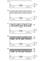
- FIG. 1 is a cross sectional view of a silicon carbide semiconductor device 100 manufactured by the method for manufacturing a silicon carbide semiconductor device according to the first embodiment. It is a figure shown in order to demonstrate the manufacturing method of the silicon carbide semiconductor device which concerns on Embodiment 1.
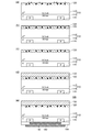
- FIG. It is a figure shown in order to demonstrate the manufacturing method of the silicon carbide semiconductor device which concerns on Embodiment 1.
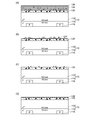
- FIG. It is a figure shown in order to demonstrate the manufacturing method of the silicon carbide semiconductor device which concerns on Embodiment 2.
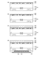
- FIG. It is a figure shown in order to demonstrate the manufacturing method of the silicon carbide semiconductor device which concerns on Embodiment 3.
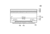
- FIG. 6 is a cross sectional view of a silicon carbide semiconductor device 102 manufactured by the method for manufacturing a silicon carbide semiconductor device according to the third embodiment. It is a normal probability distribution graph which shows the evaluation result of the silicon carbide semiconductor device which concerns on an Example, and the silicon carbide semiconductor device which concerns on a comparative example. It is a figure shown in order to demonstrate the manufacturing method of the conventional silicon carbide semiconductor device.
- FIG. 1 is a cross-sectional view of a silicon carbide semiconductor device 100 manufactured by the method for manufacturing a silicon carbide semiconductor device according to the first embodiment.
- silicon carbide semiconductor device 100 includes silicon carbide layer 110, reaction layer 120 and cathode electrode layer 130 (electrode layer of the present invention) formed on the first main surface side of silicon carbide layer 100.
- the Schottky diode includes a barrier metal layer 140, an anode electrode layer 142, and a protective insulating layer 144 formed on the second main surface side of the silicon carbide layer 100.
- Silicon carbide layer 110 has an n + type silicon carbide substrate 112 and an n ⁇ type epitaxial layer 114 containing an n type impurity at a concentration lower than that of n + type silicon carbide substrate 112.
- the thickness of the n + type silicon carbide substrate 112 is, for example, 300 ⁇ m, and the n type impurity concentration of the n + type silicon carbide substrate 112 is, for example, 1 ⁇ 10 19 cm ⁇ 3 .
- the thickness of the n ⁇ -type epitaxial layer 114 is, for example, 10 ⁇ m, and the n-type impurity concentration is, for example, 1 ⁇ 10 16 cm ⁇ 3 .
- a p-type guard ring 116 is formed on the surface of the n ⁇ -type epitaxial layer 114 on the second main surface side.
- the p-type impurity concentration of the guard ring 116 is, for example, in the range of 1 ⁇ 10 18 cm ⁇ 3 to 1 ⁇ 10 19 cm ⁇ 3 .
- Reaction layer 120 is a layer in which a nickel component is diffused into n + -type silicon carbide substrate 112.
- concentration of nickel in the reaction layer 120 is, for example, in the range of 1.0 ⁇ 10 3 cm ⁇ 3 to 1.0 ⁇ 10 4 cm ⁇ 3 , and the distance from the bonding surface between the reaction layer 120 and the cathode electrode layer 130.
- the thickness of the reaction layer 120 is, for example, in the range of 10 nm to 200 nm.
- the cathode electrode layer 130 is formed by vapor-depositing a metal (for example, nickel) as a cathode electrode material on the surface of the reaction layer 120.
- the thickness of the cathode electrode layer 130 is 2 ⁇ m, for example.
- Barrier metal layer 140 is made of a metal (eg, nickel, titanium, etc.) that forms a Schottky junction with silicon carbide layer 110 (n ⁇ type epitaxial layer 114).
- the thickness of the barrier metal layer 140 is, for example, 2 ⁇ m.
- the anode electrode layer 142 is formed on the surface of the barrier metal layer 140.
- the thickness of the anode electrode layer 142 is, for example, 5 ⁇ m.
- the anode electrode layer 142 is made of, for example, aluminum.
- a protective insulating layer 144 is formed so as to surround the barrier metal layer 140 and the anode electrode layer 142.
- Silicon carbide semiconductor device 100 having the above-described configuration can be manufactured by the following method (method for manufacturing a silicon carbide semiconductor device according to Embodiment 1). Hereinafter, the method for manufacturing the silicon carbide semiconductor device according to the first embodiment will be described along the steps.
- FIGS. 3 (a) to 3 (e) are process diagrams.
- a silicon carbide layer 110 having a structure in which an n + type silicon carbide substrate 112 and an n ⁇ type epitaxial layer 114 are stacked is prepared (see FIG. 2A).
- a p-type guard ring 116 is formed on the surface of the n ⁇ -type epitaxial layer 114.
- a conductive layer 122 made of nickel is formed on the first main surface side surface of the silicon carbide layer 110 (n + type silicon carbide substrate 112) by, for example, EB vapor deposition (FIG. 2B). )reference.).
- the thickness of the conductive layer 122 is, for example, 50 nm to 500 nm.
- a metal material other than nickel eg, aluminum, titanium, cobalt, or the like can be used.
- reaction layer 120 in contact with silicon carbide layer 110 (n + type silicon carbide substrate 112) by reacting silicon carbide layer 110 (n + type silicon carbide substrate 112) and conductive layer 122, and the reaction layer concerned A heat treatment is performed to form an alloy layer made of the silicide layer 124 existing on 120.
- the heat treatment is performed at 1000 ° C. for 2 minutes in an inert atmosphere such as high-purity argon (Ar) excluding moisture and oxygen.
- Ar high-purity argon
- the nickel component contained in conductive layer 122 diffuses into n + type silicon carbide substrate 112 to form reaction layer 120, and the silicon component and carbon component contained in n + type silicon carbide substrate 112 become conductive layers.
- a silicide layer 124 is formed by diffusing in 122 (see FIGS. 2C and 2D).
- First Plasma Ashing Step the carbon component contained in the silicide layer 124 is removed by first plasma ashing (see FIG. 2E).
- the first plasma ashing is performed using oxygen gas.
- carbon components near the surface of the silicide layer 124 are removed, so that an etching process described later can be performed efficiently.
- the nickel oxide layer 126 is formed on the surface of the silicide layer 124 by the first plasma ashing process.
- etching solution etching solution containing hydrochloric acid, nitric acid, and hydrofluoric acid
- the nickel component of the silicide layer 124 is removed by hydrochloric acid
- the silicon component is removed by nitric acid and hydrofluoric acid.
- the nickel oxide layer 126 formed by the first plasma ashing process is also removed.
- hydrochloric acid is in the range of 300 to 500 mol and hydrofluoric acid is in the range of 0.1 to 5 mol, with nitric acid being 100 mol.
- Second Plasma Ashing Step the carbon component on the surface of the reaction layer 120 is removed by second plasma ashing.
- the second plasma ashing is performed using oxygen gas. Thereby, the carbon component can be removed from the surface of the reaction layer 120.
- an oxide layer 128 is formed on the surface of the reaction layer 120 (see FIG. 3B).
- the second plasma ashing step can be performed using hydrogen gas or a mixed gas of oxygen gas and hydrogen gas instead of using oxygen gas.
- the oxide layer 128 formed in the second plasma ashing step is removed using an etching solution containing hydrofluoric acid.
- the second etching step is performed under conditions (etching time: 3 minutes) in which the oxide layer 128 formed in the second plasma ashing step is completely removed (see FIG. 3C). ).
- the cathode electrode layer 130 and the silicon carbide layer 110 to be formed later can be favorably bonded through the reaction layer 120.
- the cathode electrode layer made of nickel is formed on the surface of the reaction layer 120 by physical vapor deposition (PVD) such as sputtering. 130 is formed (see FIG. 3D).
- PVD physical vapor deposition
- a protective insulating layer 144, a barrier metal layer 140, and an anode electrode layer 142 are formed on the surface of the n ⁇ -type epitaxial layer 114 (see FIG. 3E).
- silicon carbide semiconductor device 100 can be manufactured.
- the etching process is performed using hydrochloric acid, nitric acid, and hydrofluoric acid, both the nickel component and the silicon component are removed by the etching process. It becomes possible to do. As a result, it is possible to improve the problem that the device characteristics vary due to the silicon component remaining in the etching process.
- the silicide layer is removed by using the etching process instead of the CMP process. Therefore, in the case of another conventional method for manufacturing the silicon carbide semiconductor device It becomes possible to manufacture a silicon carbide semiconductor device with higher productivity.
- the method for manufacturing the silicon carbide semiconductor device according to the first embodiment can improve the problem that the device characteristics vary due to the silicon component remaining in the etching process, and the production is high. It becomes the manufacturing method of the silicon carbide semiconductor device which can manufacture a silicon carbide semiconductor device by the property.
- the second plasma ashing for removing the carbon component that may remain on the reaction layer between the etching step and the electrode layer forming step since the process is further included, the adhesion between the reaction layer and the electrode layer can be further increased.
- the second etching for removing the oxide layer formed in the second plasma ashing process between the second plasma ashing process and the electrode layer forming process is performed under the condition that the oxide layer formed in the second plasma ashing step is completely removed, so that the resistance between the reaction layer and the electrode layer is further reduced. It becomes possible.
- FIG. 4 is a view for explaining the method for manufacturing the silicon carbide semiconductor device according to the second embodiment.
- 4A to 4D are process diagrams.
- the method for manufacturing the silicon carbide semiconductor device according to the second embodiment corresponds to FIGS. 2 (e), 3 (a), and 3 (b) in the case of the method for manufacturing the silicon carbide semiconductor device according to the first embodiment. Since the steps other than those include the same steps as those in the method for manufacturing the silicon carbide semiconductor device according to the first embodiment, the steps corresponding to FIGS. 2A to 2D and FIGS. Steps corresponding to e) are not shown.
- the method for manufacturing the silicon carbide semiconductor device according to the second embodiment basically includes the same steps as the method for manufacturing the silicon carbide semiconductor device 100 according to the first embodiment, but the content of the etching step is the carbonization according to the first embodiment. This is different from the method of manufacturing the silicon semiconductor device. That is, in the method for manufacturing the silicon carbide semiconductor device according to the second embodiment, the etching process using the etching solution A containing hydrochloric acid and the etching process using the etching solution B containing nitric acid and hydrofluoric acid are performed in this order. To do.
- the nickel oxide layer 126 formed by the first plasma ashing step and the nickel component in the silicide layer 124 are removed by the etching solution A containing hydrochloric acid (FIGS. 4A and 4). (See (b).)
- the silicon component in the silicide layer 124 is removed with an etching solution B containing nitric acid and hydrofluoric acid (see FIGS. 4B and 4C).
- etching solution B a solution in which the content ratio of nitric acid and hydrofluoric acid is within the range of 0.1 mol to 5 mol when nitric acid is 100 mol is used.
- At least a part of the surface of the reaction layer 120 is exposed by performing the first etching process and the next etching process described above.
- the second plasma ashing step (see FIG. 4D) and the electrode layer forming step (see FIGS. 3C to 3D) are sequentially performed to manufacture the silicon carbide semiconductor device 100. can do.
- the content of the etching process is different from that in the method for manufacturing the silicon carbide semiconductor device according to the first embodiment, but the silicon carbide according to the first embodiment.
- the etching process is performed using hydrochloric acid, nitric acid, and hydrofluoric acid, so that both the nickel component and the silicon component can be removed by the etching process. Become. As a result, the device characteristics do not vary due to the silicon component remaining in the etching process.
- the silicide layer is removed by using the etching process instead of the CMP process. Therefore, in the case of another conventional method for manufacturing a silicon carbide semiconductor device It becomes possible to manufacture a silicon carbide semiconductor device with higher productivity.
- the method for manufacturing the silicon carbide semiconductor device according to the second embodiment is similar to the method for manufacturing the silicon carbide semiconductor device according to the first embodiment due to the fact that the silicon component remains in the etching process.
- a silicon carbide semiconductor device manufacturing method capable of improving the problem of variation in the thickness and manufacturing a silicon carbide semiconductor device with high productivity is provided.
- the manufacturing method of the silicon carbide semiconductor device which concerns on Embodiment 2 includes the process similar to the manufacturing method of the silicon carbide semiconductor device which concerns on Embodiment 1 except an etching process, the silicon carbide semiconductor device which concerns on Embodiment 1 of FIG. It has the corresponding effect as it is among the effects of the manufacturing method.
- FIG. 5 is a view for explaining the method for manufacturing the silicon carbide semiconductor device according to the third embodiment.
- FIG. 5A to FIG. 5D are process diagrams.
- FIG. 6 is a cross-sectional view of silicon carbide semiconductor device 102 manufactured by the method for manufacturing the silicon carbide semiconductor device according to the third embodiment.
- the method for manufacturing the silicon carbide semiconductor device according to the third embodiment corresponds to FIGS. 2 (a) to 2 (e) and FIG. 3 (a) in the case of the method for manufacturing the silicon carbide semiconductor device according to the first embodiment. Includes steps similar to those of the method for manufacturing the silicon carbide semiconductor device according to the first embodiment, and therefore, the steps corresponding to FIGS. 2A to 2E and FIG.
- the method for manufacturing the silicon carbide semiconductor device according to the third embodiment basically includes the same steps as the method for manufacturing the silicon carbide semiconductor device 100 according to the first embodiment, but the contents of the second etching step are the same as those of the first embodiment. This is different from the method of manufacturing the silicon carbide semiconductor device. That is, in the method for manufacturing the silicon carbide semiconductor device according to the third embodiment, the second etching step is performed under the condition that a part of the oxide layer 128 formed in the second plasma ashing step remains. Specifically, the second etching step is performed for a shorter time (etching time: 3 minutes ⁇ 2 minutes) than in the method for manufacturing the silicon carbide semiconductor device according to the first embodiment.
- electrode layer 130 is not directly formed on the surface of reaction layer 120, but a reaction layer. It is formed above 120 via a very thin conductive oxide layer 129.
- the method for manufacturing the silicon carbide semiconductor device according to the third embodiment differs from the method for manufacturing the silicon carbide semiconductor device according to the first embodiment in the content of the second etching step, but the carbonization according to the first embodiment.
- the etching process is performed using hydrochloric acid, nitric acid and hydrofluoric acid, so that both the nickel component and the silicon component can be removed by the etching process. It becomes. As a result, the device characteristics do not vary due to the silicon component remaining in the etching process.
- the silicide layer is removed using an etching process instead of a CMP process, and therefore, in the case of another conventional method for manufacturing a silicon carbide semiconductor device It becomes possible to manufacture a silicon carbide semiconductor device with higher productivity.
- the method for manufacturing the silicon carbide semiconductor device according to the third embodiment is similar to the method for manufacturing the silicon carbide semiconductor device according to the first embodiment because the silicon component remains in the etching process.
- a silicon carbide semiconductor device manufacturing method capable of improving the problem of variation in the thickness and manufacturing a silicon carbide semiconductor device with high productivity is provided.
- the silicon carbide semiconductor having a structure in which the electrode layer 130 is formed above the reaction layer 120 via the extremely thin conductive oxide layer 129. Since device 102 can be manufactured, the reaction layer and the electrode are compared with the case of silicon carbide semiconductor device (silicon carbide semiconductor device 100) having a structure in which electrode layer 130 is formed directly on the surface of reaction layer 120. It becomes possible to further reduce the resistance between the layers.
- the manufacturing method of the silicon carbide semiconductor device which concerns on Embodiment 3 includes the process similar to the manufacturing method of the silicon carbide semiconductor device which concerns on Embodiment 1 except a 2nd etching process, the silicon carbide semiconductor which concerns on Embodiment 1 It has the corresponding effect as it is among the effects of the device manufacturing method.
- Example According to the present embodiment, “According to the method for manufacturing a silicon carbide semiconductor device of the present invention, it is possible to improve the problem that the device characteristics vary due to the silicon component remaining in the etching process. This is an example for explaining. A forward voltage drop VF was used as device characteristics.
- Sample A silicon carbide semiconductor device manufactured by the method for manufacturing a silicon carbide semiconductor device according to Embodiment 1 was taken as an example.
- a silicon carbide semiconductor device manufactured by the same method was used as a comparative example.
- the silicon carbide semiconductor device according to the example and the silicon carbide semiconductor device according to the comparative example are evaluated by preparing 60 silicon carbide semiconductor devices according to the example and the silicon carbide semiconductor device according to the comparative example, respectively.
- the direction drop voltage VF was measured, and the obtained forward drop voltage VF was plotted on a normal probability distribution graph. In this case, the larger the upward slope in the normal probability distribution graph, the smaller the variation.
- FIG. 7 is a normal probability distribution graph showing evaluation results of the silicon carbide semiconductor device according to the example and the silicon carbide semiconductor device according to the comparative example. As is clear from FIG. 7, it was found that the silicon carbide semiconductor device according to the example had smaller variations in device characteristics (forward voltage drop VF) than the silicon carbide semiconductor device according to the comparative example. That is, according to this example, “the method of manufacturing a silicon carbide semiconductor device of the present invention can improve the problem that the device characteristics vary due to the remaining silicon component in the etching process. It is clear.
- the etching process using the etching solution A containing hydrochloric acid and the etching process using the etching solution B containing nitric acid and hydrofluoric acid are performed in this order. It is not limited to this.
- the etching process using the etching solution B containing nitric acid and hydrofluoric acid and the etching process using the etching solution A containing hydrochloric acid may be performed in this order.
- the first plasma ashing step and the second plasma ashing step are performed using oxygen gas, but the present invention is not limited to this.
- the first plasma ashing process and the second plasma ashing process may be performed using “hydrogen gas” or “mixed gas of oxygen gas and hydrogen gas” instead of oxygen gas.
- the entire surface of the reaction layer 120 is exposed by removing the silicide layer 124 from the reaction layer 120, and then the electrode layer 130 is formed on the surface of the reaction layer 120.
- the present invention is not limited to this.
- a part of the surface of the reaction layer may be exposed by removing a part of the silicide layer from the reaction layer, and then an electrode layer may be formed on the surface of the reaction layer.
- a part of the oxide layer formed in the second plasma ashing process is left by shortening the time of the second etching process, but the present invention is not limited to this. It is not something.
- a part of the oxide layer formed in the second plasma ashing process may be left by reducing the concentration of hydrofluoric acid contained in the etching solution used in the second etching process.
- a part of the oxide layer (conductive oxide layer) formed in the second plasma ashing process is left by shortening the time of the second etching process.
- the invention is not limited to this.
- the second etching step is omitted, and the surface of the reaction layer 120 is simply cleaned (acid cleaning and diluted hydrofluoric acid cleaning) before the cathode electrode layer forming step is performed, thereby forming the second plasma ashing step.
- the oxidized layer (conductive oxide layer) may be removed while leaving a part thereof.
- the present invention has been described by taking as an example the case where a single electrode layer (cathode electrode layer 130) is formed on the reaction layer 120, but the present invention is not limited to this. .
- the present invention can also be applied when a plurality of electrode layers are formed on the reaction layer.
- the method for manufacturing a silicon carbide semiconductor device of the present invention has been described by taking a Schottky diode as an example, but the present invention is not limited to this.
- the present invention can be applied to a method for manufacturing a silicon carbide semiconductor device including a step of forming an electrode layer on a silicon carbide layer via a reaction layer, such as a power MOSFET, an IGBT, a pn diode, and a thyristor.
- the present invention has been described by taking the case of an n-type silicon carbide layer as an example, but the present invention is not limited to this.
- the present invention can be applied when a p-type silicon carbide layer is used.
- 100,102,900 ... silicon carbide semiconductor device 110,910 ... silicon carbide layer, 112,912 ... n + -type silicon carbide substrate, 114 ... n - -type epitaxial layer, 116 ... guard ring, 120,920 ... reaction layer, 122, 922 ... conductive layer, 124, 924 ... silicide layer, 126 ... nickel oxide layer, 128 ... oxide layer, 129 ... very thin conductive oxide layer, 130 ... cathode electrode layer, 140 ... barrier metal layer, 142 ... anode Electrode layer, 144 ... Protective insulating layer, 930 ... Electrode layer, 932 ... Other electrode layers
Landscapes
- Electrodes Of Semiconductors (AREA)
- Engineering & Computer Science (AREA)
- Physics & Mathematics (AREA)
- Plasma & Fusion (AREA)
- Chemical & Material Sciences (AREA)
- Materials Engineering (AREA)
Abstract
Description
図1は、実施形態1に係る炭化珪素半導体装置の製造方法により製造する炭化珪素半導体装置100の断面図である。
炭化珪素半導体装置100は、図1に示すように、炭化珪素層110と、炭化珪素層100の第1主面側に形成された反応層120及びカソード電極層130(本発明の電極層)と、炭化珪素層100の第2主面側に形成されたバリアメタル層140及びアノード電極層142並びに保護絶縁層144とを備えるショットキーダイオードである。
まず、n+型炭化珪素基板112とn-型エピタキシャル層114とが積層された構造を有する炭化珪素層110を準備する(図2(a)参照。)。n-型エピタキシャル層114の表面には、p型のガードリング116が形成されている。
次に、炭化珪素層110(n+型炭化珪素基板112)の第1主面側の表面上に、例えばEB蒸着により、ニッケルからなる導電層122を形成する(図2(b)参照。)。導電層122の厚さは、例えば50nm~500nmとする。導電層122の材料としては、ニッケル以外の金属材料(例えば、アルミニウム、チタン、コバルトなど。)を用いることもできる。
次に、炭化珪素層110(n+型炭化珪素基板112)と導電層122とを反応させて、炭化珪素層110(n+型炭化珪素基板112)に接する反応層120及び当該反応層120上に存在するシリサイド層124からなる合金層を形成する熱処理を行う。熱処理は、水分や酸素を除いた高純度のアルゴン(Ar)等の不活性雰囲気中で1000℃、2分間の条件で行う。
これにより、導電層122に含まれるニッケル成分がn+型炭化珪素基板112中に拡散して反応層120を形成するとともに、n+型炭化珪素基板112に含まれるシリコン成分及び炭素成分が導電層122中に拡散してシリサイド層124を形成する(図2(c)及び図2(d)参照。)。
次に、シリサイド層124に含まれる炭素成分を第1プラズマアッシングにより除去する(図2(e)参照。)。第1プラズマアッシングは、酸素ガスを用いて実施する。当該第1プラズマアッシング工程を行うことにより、シリサイド層124の表面付近の炭素成分が除去されるため、後述するエッチング工程を効率よく行うことができる。なお、このとき、第1プラズマアッシング工程により、シリサイド層124の表面に酸化ニッケル層126が形成される。
次に、塩酸、硝酸及びフッ酸を含有するエッチング液(エッチング液)によりシリサイド層124を除去することにより、反応層120の表面を露出させる(図3(a)参照。)。
当該エッチング工程中、塩酸によりシリサイド層124のうちニッケル成分が除去され、また、硝酸及びフッ酸によりシリコン成分が除去される。また、当該エッチング工程においては、第1プラズマアッシング工程により形成された酸化ニッケル層126も除去される。エッチング液が含有する塩酸、硝酸及びフッ酸の含有比率は、硝酸を100molとしたとき、塩酸が300mol~500molの範囲内にあり、フッ酸が0.1mol~5molの範囲内にある。
次に、反応層120の表面の炭素成分を第2プラズマアッシングにより除去する。第2プラズマアッシングは、酸素ガスを用いて実施する。これにより、反応層120の表面から炭素成分を除去することが可能となる。第2プラズマアッシング工程中に、反応層120の表面に酸化層128が形成される(図3(b)参照。)。なお、第2プラズマアッシング工程は、酸素ガスを用いる代わりに水素ガス又は酸素ガス及び水素ガスの混合ガスを用いて実施することもできる。
次に、フッ酸を含有するエッチング液を用いて、第2プラズマアッシング工程で形成された酸化層128を除去する。当該第2エッチング工程においては、第2プラズマアッシング工程で形成された酸化層128が完全に除去される条件(エッチング時間:3分)で第2エッチング工程を実施する(図3(c)参照。)。当該第2エッチング工程によって、後に形成するカソード電極層130と炭化珪素層110とを反応層120を介して良好に接合できるようになる。
次に、反応層120の表面を洗浄(酸洗浄)した後、反応層120の表面上に、例えばスパッタリングなどの物理気相成長法(PVD)により、ニッケルからなるカソード電極層130を形成する(図3(d)参照。)。
図4は、実施形態2に係る炭化珪素半導体装置の製造方法を説明するために示す図である。図4(a)~図4(d)は各工程図である。実施形態2に係る炭化珪素半導体装置の製造方法は、実施形態1に係る炭化珪素半導体装置の製造方法の場合における図2(e)、図3(a)及び図3(b)に対応する工程以外の工程は、実施形態1に係る炭化珪素半導体装置の製造方法と同様の工程を含むため、図2(a)~図2(d)に対応する工程及び図3(c)~図3(e)に対応する工程は図示を省略する。
図5は、実施形態3に係る炭化珪素半導体装置の製造方法を説明するために示す図である。図5(a)~図5(d)は各工程図である。図6は、実施形態3に係る炭化珪素半導体装置の製造方法により製造された炭化珪素半導体装置102の断面図である。
実施形態3に係る炭化珪素半導体装置の製造方法は、実施形態1に係る炭化珪素半導体装置の製造方法の場合における図2(a)~図2(e)及び図3(a)に対応する工程は、実施形態1に係る炭化珪素半導体装置の製造方法と同様の工程を含むため、図2(a)~図2(e)及び図3(a)に対応する工程は図示を省略する。
本実施例は、「本発明の炭化珪素半導体装置の製造方法によれば、エッチング工程でシリコン成分が残存することに起因してデバイス特性にばらつきが生じるという問題を改善することが可能である。」ことを説明するための実施例である。デバイス特性としては順方向降下電圧VFを用いた。
実施形態1に係る炭化珪素半導体装置の製造方法により製造した炭化珪素半導体装置を実施例とした。一方、塩酸及び過酸化水素水を含有するエッチング液(塩酸:過酸化水素水=5:1)を用いてエッチング工程を実施したこと以外は、実施形態1に係る炭化珪素半導体装置の製造方法と同様の方法により製造した炭化珪素半導体装置を比較例とした。
実施例に係る炭化珪素半導体装置及び比較例に係る炭化珪素半導体装置の評価は、実施例に係る炭化珪素半導体装置及び比較例に係る炭化珪素半導体装置をそれぞれ60個準備し、これらの順方向降下電圧VFを測定し、得られた順方向降下電圧VFを正規確率分布グラフにプロットすることにより行った。この場合、正規確率分布グラフにおいて右上がりの傾きが大きいほどばらつきが小さいことを示す。
図7は、実施例に係る炭化珪素半導体装置及び比較例に係る炭化珪素半導体装置の評価結果を示す正規確率分布グラフである。
図7からも明らかなように、実施例に係る炭化珪素半導体装置は、比較例に係る炭化珪素半導体装置よりも、デバイス特性(順方向降下電圧VF)のばらつきが小さいことが分かった。すなわち、本実施例により、「本発明の炭化珪素半導体装置の製造方法によれば、エッチング工程でシリコン成分が残存することに起因してデバイス特性にばらつきが生じるという問題を改善することが可能である。」ことが明らかとなった。
Claims (9)
- 炭化珪素層上に導電層を形成する導電層形成工程と、
前記炭化珪素層と前記導電層とを反応させて、前記炭化珪素層に接する反応層及び前記反応層上に存在するシリサイド層を形成する熱処理工程と、
前記シリサイド層が含有する炭素成分を除去するための第1プラズマアッシング工程と、
塩酸、硝酸及びフッ酸を用いて前記シリサイド層の少なくとも一部を除去することにより、前記反応層の表面の少なくとも一部を露出させるエッチング工程と、
露出させた前記反応層の上方に電極層を形成する電極層形成工程とをこの順で含むことを特徴とする炭化珪素半導体装置の製造方法。 - 請求項1に記載の炭化珪素半導体装置の製造方法において、
塩酸、硝酸及びフッ酸を含有するエッチング液を用いて前記エッチング工程を実施することを特徴とする炭化珪素半導体装置の製造方法。 - 請求項2に記載の炭化珪素半導体装置の製造方法において、
前記エッチング液が含有する塩酸、硝酸及びフッ酸の含有比率は、硝酸を100molとしたとき、塩酸が300mol~500molの範囲内にあり、フッ酸が0.1mol~5molの範囲内にあることを特徴とする炭化珪素半導体装置の製造方法。 - 請求項1に記載の炭化珪素半導体装置の製造方法において、
前記エッチング工程は、塩酸を含有するエッチング液Aを用いるエッチング工程と、硝酸及びフッ酸を含有するエッチング液Bを用いるエッチング工程とを含むことを特徴とする炭化珪素半導体装置の製造方法。 - 請求項4に記載の炭化珪素半導体装置の製造方法において、
前記エッチング液Bが含有する硝酸及びフッ酸の含有比率は、硝酸を100molとしたとき、フッ酸が0.1mol~5molの範囲内にあることを特徴とする炭化珪素半導体装置の製造方法。 - 請求項1~5に記載の炭化珪素半導体装置の製造方法において、
酸素ガス、水素ガス又はこれらの混合ガスのいずれかを用いて前記第1プラズマアッシング工程を実施することを特徴とする炭化珪素半導体装置の製造方法。 - 請求項1~6のいずれかに記載の炭化珪素半導体装置の製造方法において、
前記エッチング工程と前記電極層形成工程との間に、前記反応層上に残存することがある炭素成分を除去するための第2プラズマアッシング工程をさらに含むことを特徴とする炭化珪素半導体装置の製造方法。 - 請求項7に記載の炭化珪素半導体装置の製造方法において、
酸素ガス、水素ガス又はこれらの混合ガスのいずれかを用いて前記第2プラズマアッシング工程を実施することを特徴とする炭化珪素半導体装置の製造方法。 - 請求項7又は8に記載の炭化珪素半導体装置の製造方法において、
前記第2プラズマアッシング工程と前記電極層形成工程との間に、前記第2プラズマアッシング工程で形成された酸化層を除去する第2エッチング工程をさらに含むことを特徴とする炭化珪素半導体装置の製造方法。
Priority Applications (4)
| Application Number | Priority Date | Filing Date | Title |
|---|---|---|---|
| CN201180046423.1A CN103140916B (zh) | 2011-04-11 | 2011-09-09 | 碳化硅半导体装置的制造方法 |
| EP11863268.6A EP2698807B1 (en) | 2011-04-11 | 2011-09-09 | Method for producing silicon carbide semiconductor device |
| US13/884,166 US9005462B2 (en) | 2011-04-11 | 2011-09-09 | Method for manufacturing silicon carbide semiconductor device |
| JP2013509730A JP5427980B2 (ja) | 2011-04-11 | 2011-09-09 | 炭化珪素半導体装置の製造方法 |
Applications Claiming Priority (2)
| Application Number | Priority Date | Filing Date | Title |
|---|---|---|---|
| JP2011-086984 | 2011-04-11 | ||
| JP2011086984 | 2011-04-11 |
Publications (1)
| Publication Number | Publication Date |
|---|---|
| WO2012140794A1 true WO2012140794A1 (ja) | 2012-10-18 |
Family
ID=47008994
Family Applications (2)
| Application Number | Title | Priority Date | Filing Date |
|---|---|---|---|
| PCT/JP2011/070591 Ceased WO2012140795A1 (ja) | 2011-04-11 | 2011-09-09 | 炭化珪素半導体装置及びその製造方法 |
| PCT/JP2011/070590 Ceased WO2012140794A1 (ja) | 2011-04-11 | 2011-09-09 | 炭化珪素半導体装置の製造方法 |
Family Applications Before (1)
| Application Number | Title | Priority Date | Filing Date |
|---|---|---|---|
| PCT/JP2011/070591 Ceased WO2012140795A1 (ja) | 2011-04-11 | 2011-09-09 | 炭化珪素半導体装置及びその製造方法 |
Country Status (5)
| Country | Link |
|---|---|
| US (2) | US9224645B2 (ja) |
| EP (2) | EP2698807B1 (ja) |
| JP (2) | JP5427980B2 (ja) |
| CN (2) | CN103229275B (ja) |
| WO (2) | WO2012140795A1 (ja) |
Cited By (1)
| Publication number | Priority date | Publication date | Assignee | Title |
|---|---|---|---|---|
| JP2016136589A (ja) * | 2015-01-23 | 2016-07-28 | 三菱電機株式会社 | 基板、基板の製造方法 |
Families Citing this family (12)
| Publication number | Priority date | Publication date | Assignee | Title |
|---|---|---|---|---|
| EP2698807B1 (en) * | 2011-04-11 | 2015-09-23 | Shindengen Electric Manufacturing Co., Ltd. | Method for producing silicon carbide semiconductor device |
| DE102012213077A1 (de) * | 2012-07-25 | 2014-01-30 | Robert Bosch Gmbh | Verfahren zum Kontaktieren eines Halbleitermaterials mit einer Kontaktlage |
| JP6222771B2 (ja) * | 2013-11-22 | 2017-11-01 | 国立研究開発法人産業技術総合研究所 | 炭化珪素半導体装置の製造方法 |
| CN204966510U (zh) | 2014-06-20 | 2016-01-13 | 意法半导体股份有限公司 | 宽带隙高密度半导体开关器件 |
| JP2016219475A (ja) * | 2015-05-15 | 2016-12-22 | トヨタ自動車株式会社 | 炭化珪素半導体装置の製造方法 |
| EP3389082B1 (en) * | 2015-12-11 | 2020-10-28 | Shindengen Electric Manufacturing Co., Ltd. | Method for manufacturing silicon carbide semiconductor device |
| JP6584966B2 (ja) * | 2016-01-12 | 2019-10-02 | 株式会社東芝 | 半導体装置、半導体装置の製造方法、インバータ回路、駆動装置、車両、及び昇降機 |
| CN105514178A (zh) * | 2016-02-03 | 2016-04-20 | 泰州优宾晶圆科技有限公司 | 一种沟槽式mos肖特基二极管 |
| CN108717945B (zh) * | 2018-05-24 | 2022-01-07 | 西安理工大学 | 一种具有NiO/SiC异质发射结的SiC光触发晶闸管 |
| CN111276395A (zh) * | 2020-02-19 | 2020-06-12 | 华芯威半导体科技(北京)有限责任公司 | 一种碳化硅器件原料的制造方法及使用该原料制备的碳化硅器件 |
| DE102022209805A1 (de) | 2022-09-19 | 2024-03-21 | Robert Bosch Gesellschaft mit beschränkter Haftung | Verfahren zum Erzeugen eines elektrischen Kontaktes, Halbleiteranordnung und Halbleiterbauelement |
| WO2025234936A1 (en) * | 2024-05-08 | 2025-11-13 | Agency For Science, Technology And Research | Stacked arrangement and method of forming the same |
Citations (6)
| Publication number | Priority date | Publication date | Assignee | Title |
|---|---|---|---|---|
| JP2003243323A (ja) * | 2001-12-14 | 2003-08-29 | Matsushita Electric Ind Co Ltd | 半導体素子およびその製造方法 |
| JP2006024880A (ja) | 2004-06-09 | 2006-01-26 | Matsushita Electric Ind Co Ltd | 半導体装置及びその製造方法 |
| JP2006261624A (ja) * | 2005-03-14 | 2006-09-28 | Denso Corp | ワイドバンド半導体のオーミック接続形成方法 |
| JP2008053291A (ja) * | 2006-08-22 | 2008-03-06 | Rohm Co Ltd | SiC半導体素子およびその製造方法 |
| JP2009010096A (ja) | 2007-06-27 | 2009-01-15 | Nissan Motor Co Ltd | 炭化珪素半導体装置とその製造方法 |
| JP2010205824A (ja) * | 2009-03-02 | 2010-09-16 | Denso Corp | 炭化珪素半導体装置の製造方法 |
Family Cites Families (15)
| Publication number | Priority date | Publication date | Assignee | Title |
|---|---|---|---|---|
| JP3117446B2 (ja) | 1989-06-15 | 2000-12-11 | 株式会社半導体エネルギー研究所 | 酸化物導電膜の成膜加工方法 |
| US6051283A (en) * | 1998-01-13 | 2000-04-18 | International Business Machines Corp. | Microwave annealing |
| JP2000101064A (ja) * | 1998-09-25 | 2000-04-07 | Sanyo Electric Co Ltd | 電極、SiCの電極及びSiCデバイス |
| US6207565B1 (en) * | 2000-01-13 | 2001-03-27 | Vlsi Technology, Inc | Integrated process for ashing resist and treating silicon after masked spacer etch |
| JP3650727B2 (ja) * | 2000-08-10 | 2005-05-25 | Hoya株式会社 | 炭化珪素製造方法 |
| JP2002217129A (ja) * | 2001-01-18 | 2002-08-02 | New Japan Radio Co Ltd | シリコンカーバイド半導体装置の製造方法 |
| WO2002090615A1 (en) * | 2001-05-04 | 2002-11-14 | Lam Research Corporation | Duo-step plasma cleaning of chamber residues |
| TW591217B (en) * | 2003-07-17 | 2004-06-11 | South Epitaxy Corp | UV detector |
| US20070138482A1 (en) * | 2005-12-08 | 2007-06-21 | Nissan Motor Co., Ltd. | Silicon carbide semiconductor device and method for producing the same |
| KR100860367B1 (ko) * | 2006-08-21 | 2008-09-25 | 제일모직주식회사 | 금속실리사이드막 대비 실리콘 산화막에 대한 상대적인 식각 선택성이 향상된 식각용액 |
| JP5014749B2 (ja) * | 2006-11-27 | 2012-08-29 | 三菱電機株式会社 | 炭化珪素半導体装置の製造方法 |
| JP5282382B2 (ja) | 2007-08-17 | 2013-09-04 | 富士電機株式会社 | 炭化珪素半導体装置、その製造方法および炭化珪素デバイス |
| JP2009194216A (ja) * | 2008-02-15 | 2009-08-27 | Hitachi Ltd | 半導体装置の製造方法 |
| US20120161098A1 (en) * | 2009-08-20 | 2012-06-28 | Nec Corporation | Substrate, manufacturing method of substrate, semiconductor element, and manufacturing method of semiconductor element |
| EP2698807B1 (en) * | 2011-04-11 | 2015-09-23 | Shindengen Electric Manufacturing Co., Ltd. | Method for producing silicon carbide semiconductor device |
-
2011
- 2011-09-09 EP EP11863268.6A patent/EP2698807B1/en active Active
- 2011-09-09 WO PCT/JP2011/070591 patent/WO2012140795A1/ja not_active Ceased
- 2011-09-09 WO PCT/JP2011/070590 patent/WO2012140794A1/ja not_active Ceased
- 2011-09-09 JP JP2013509730A patent/JP5427980B2/ja active Active
- 2011-09-09 JP JP2013509731A patent/JP5415650B2/ja active Active
- 2011-09-09 US US13/980,998 patent/US9224645B2/en active Active
- 2011-09-09 EP EP11863270.2A patent/EP2698808B1/en active Active
- 2011-09-09 CN CN201180046431.6A patent/CN103229275B/zh active Active
- 2011-09-09 US US13/884,166 patent/US9005462B2/en active Active
- 2011-09-09 CN CN201180046423.1A patent/CN103140916B/zh active Active
Patent Citations (6)
| Publication number | Priority date | Publication date | Assignee | Title |
|---|---|---|---|---|
| JP2003243323A (ja) * | 2001-12-14 | 2003-08-29 | Matsushita Electric Ind Co Ltd | 半導体素子およびその製造方法 |
| JP2006024880A (ja) | 2004-06-09 | 2006-01-26 | Matsushita Electric Ind Co Ltd | 半導体装置及びその製造方法 |
| JP2006261624A (ja) * | 2005-03-14 | 2006-09-28 | Denso Corp | ワイドバンド半導体のオーミック接続形成方法 |
| JP2008053291A (ja) * | 2006-08-22 | 2008-03-06 | Rohm Co Ltd | SiC半導体素子およびその製造方法 |
| JP2009010096A (ja) | 2007-06-27 | 2009-01-15 | Nissan Motor Co Ltd | 炭化珪素半導体装置とその製造方法 |
| JP2010205824A (ja) * | 2009-03-02 | 2010-09-16 | Denso Corp | 炭化珪素半導体装置の製造方法 |
Non-Patent Citations (1)
| Title |
|---|
| See also references of EP2698807A4 |
Cited By (2)
| Publication number | Priority date | Publication date | Assignee | Title |
|---|---|---|---|---|
| JP2016136589A (ja) * | 2015-01-23 | 2016-07-28 | 三菱電機株式会社 | 基板、基板の製造方法 |
| US10249500B2 (en) | 2015-01-23 | 2019-04-02 | Mitsubishi Electric Corporation | Method for manufacturing substrate for semiconductor device |
Also Published As
| Publication number | Publication date |
|---|---|
| US9224645B2 (en) | 2015-12-29 |
| EP2698807B1 (en) | 2015-09-23 |
| CN103229275A (zh) | 2013-07-31 |
| CN103140916B (zh) | 2015-06-10 |
| EP2698808A1 (en) | 2014-02-19 |
| EP2698807A4 (en) | 2014-09-10 |
| EP2698808B1 (en) | 2018-12-05 |
| CN103140916A (zh) | 2013-06-05 |
| US20130244428A1 (en) | 2013-09-19 |
| EP2698808A4 (en) | 2015-02-18 |
| US9005462B2 (en) | 2015-04-14 |
| JP5415650B2 (ja) | 2014-02-12 |
| EP2698807A1 (en) | 2014-02-19 |
| JPWO2012140795A1 (ja) | 2014-07-28 |
| JP5427980B2 (ja) | 2014-02-26 |
| US20130306992A1 (en) | 2013-11-21 |
| JPWO2012140794A1 (ja) | 2014-07-28 |
| CN103229275B (zh) | 2015-10-07 |
| WO2012140795A1 (ja) | 2012-10-18 |
Similar Documents
| Publication | Publication Date | Title |
|---|---|---|
| JP5427980B2 (ja) | 炭化珪素半導体装置の製造方法 | |
| JP6099298B2 (ja) | SiC半導体デバイス及びその製造方法 | |
| CN104272442B (zh) | 半导体器件的制造方法 | |
| JP5525940B2 (ja) | 半導体装置および半導体装置の製造方法 | |
| JP5728339B2 (ja) | 半導体装置および半導体装置の製造方法 | |
| JP5449786B2 (ja) | 炭化珪素半導体装置及び炭化珪素半導体装置の製造方法 | |
| JP2014110362A (ja) | 炭化珪素半導体装置及びその製造方法 | |
| JP5369581B2 (ja) | 半導体デバイス用裏面電極、半導体デバイスおよび半導体デバイス用裏面電極の製造方法 | |
| JP5600985B2 (ja) | 電力半導体装置の製造方法 | |
| JP4091931B2 (ja) | SiC半導体装置およびSiC半導体装置の製造方法 | |
| JP2021097085A (ja) | 半導体装置及びその製造方法 | |
| JP5775711B2 (ja) | 炭化珪素半導体装置及びその製造方法 | |
| JP6151135B2 (ja) | 半導体装置及びその製造方法 | |
| JP2006093206A (ja) | SiC半導体装置およびSiC半導体装置の製造方法 | |
| CN113169055A (zh) | 半导体装置及半导体装置的制造方法 |
Legal Events
| Date | Code | Title | Description |
|---|---|---|---|
| WWE | Wipo information: entry into national phase |
Ref document number: 201180046423.1 Country of ref document: CN |
|
| 121 | Ep: the epo has been informed by wipo that ep was designated in this application |
Ref document number: 11863268 Country of ref document: EP Kind code of ref document: A1 |
|
| ENP | Entry into the national phase |
Ref document number: 2013509730 Country of ref document: JP Kind code of ref document: A |
|
| WWE | Wipo information: entry into national phase |
Ref document number: 13884166 Country of ref document: US |
|
| WWE | Wipo information: entry into national phase |
Ref document number: 2011863268 Country of ref document: EP |
|
| NENP | Non-entry into the national phase |
Ref country code: DE |