WO2012143968A1 - Survolteur - Google Patents
Survolteur Download PDFInfo
- Publication number
- WO2012143968A1 WO2012143968A1 PCT/JP2011/002259 JP2011002259W WO2012143968A1 WO 2012143968 A1 WO2012143968 A1 WO 2012143968A1 JP 2011002259 W JP2011002259 W JP 2011002259W WO 2012143968 A1 WO2012143968 A1 WO 2012143968A1
- Authority
- WO
- WIPO (PCT)
- Prior art keywords
- voltage
- parallel
- switch
- pair
- voltage booster
- Prior art date
- Legal status (The legal status is an assumption and is not a legal conclusion. Google has not performed a legal analysis and makes no representation as to the accuracy of the status listed.)
- Ceased
Links
Images


Classifications
-
- H—ELECTRICITY
- H02—GENERATION; CONVERSION OR DISTRIBUTION OF ELECTRIC POWER
- H02M—APPARATUS FOR CONVERSION BETWEEN AC AND AC, BETWEEN AC AND DC, OR BETWEEN DC AND DC, AND FOR USE WITH MAINS OR SIMILAR POWER SUPPLY SYSTEMS; CONVERSION OF DC OR AC INPUT POWER INTO SURGE OUTPUT POWER; CONTROL OR REGULATION THEREOF
- H02M3/00—Conversion of DC power input into DC power output
- H02M3/02—Conversion of DC power input into DC power output without intermediate conversion into AC
- H02M3/04—Conversion of DC power input into DC power output without intermediate conversion into AC by static converters
- H02M3/10—Conversion of DC power input into DC power output without intermediate conversion into AC by static converters using discharge tubes with control electrode or semiconductor devices with control electrode
- H02M3/145—Conversion of DC power input into DC power output without intermediate conversion into AC by static converters using discharge tubes with control electrode or semiconductor devices with control electrode using devices of a triode or transistor type requiring continuous application of a control signal
- H02M3/155—Conversion of DC power input into DC power output without intermediate conversion into AC by static converters using discharge tubes with control electrode or semiconductor devices with control electrode using devices of a triode or transistor type requiring continuous application of a control signal using semiconductor devices only
- H02M3/156—Conversion of DC power input into DC power output without intermediate conversion into AC by static converters using discharge tubes with control electrode or semiconductor devices with control electrode using devices of a triode or transistor type requiring continuous application of a control signal using semiconductor devices only with automatic control of output voltage or current, e.g. switching regulators
- H02M3/158—Conversion of DC power input into DC power output without intermediate conversion into AC by static converters using discharge tubes with control electrode or semiconductor devices with control electrode using devices of a triode or transistor type requiring continuous application of a control signal using semiconductor devices only with automatic control of output voltage or current, e.g. switching regulators including plural semiconductor devices as final control devices for a single load
Definitions
- the present invention relates to a voltage booster capable of applying a boosted voltage to an electric load, for example a motor-driving circuit including an inverter or a power converter, which drives an electric rotating machine.
- the inverter for driving a synchronous motor or an asynchronous motor and the power converter for driving a switched reluctance motor need to boost a battery voltage, when the motors are provided for a variable-speed application such as a traction motor of an electric vehicle or a hybrid vehicle.
- the switched reluctance motor needs to increase and decrease phase currents quickly.
- the phase currents of the SRM rises up and falls down quickly, when the DC link voltage applied to the power converter is increased.
- FIG. 1 shows a voltage booster 200, which is well-known as a chopper type DC/DC converter.
- the voltage booster 200 boosts a battery voltage of the battery 100.
- the boosted DC link voltage Vx is applied to a motor-driving circuit 300 and a smoothing capacitor 400.
- the chopper type DC/DC converter consists of a reactor 201, an output switch 202 and a parallel switch 203.
- the motor-driving circuit 300 consisting of the multi-phase inverter or the multi-phase asynchronous power converter applies a multi-phase voltage to a synchronous motor or an asynchronous motor or a switched reluctance motor, which is not illustrated.
- FIG. 2 shows a parallel type voltage booster proposed in Japan Unexamined Patent Publication No. JPA 2004/234476.
- a battery voltage of battery 100 is boosted by a dual chopper type DC/DC converter 600.
- a first chopper consists of a reactor 601, a parallel switch 604 and an output switch 605.
- a second chopper consists of a reactor 602, a parallel switch 603 and an output switch 606.
- Two boost choppers connected in parallel apply two boost voltages to the motor-driving circuit 300 alternately. Ripple of the boosted DC link voltage Vx is reduced.
- An object of the invention is to provide a voltage booster capable of boosting an output voltage of a DC power source for applying an increased voltage to an electrical load.
- a voltage booster has at least two pairs consisting of a reactor and a DC power source each.
- Each parallel switch is connected in parallel to each pair in order to short-circuit each pair.
- the short-circuit current has an opposite direction to an output current of the voltage booster. Accordingly, a power loss of the PWM-switched parallel switches of the voltage booster is reduced largely.
- a first middle voltage mode (C) and a second middle voltage mode (D) alternately.
- the parallel switch (120) is turned on, and the parallel switch (130) is turned off, in the first middle voltage mode (C).
- the parallel switch (120) is turned off, and the parallel switch (130) is turned on, in the second middle voltage mode (D). Accordingly, a power loss of the parallel switches is reduced largely.
- the voltage booster further has a high voltage mode (A) and a low voltage mode (B) alternately.
- the parallel switches (120 and 130) are turned off in the high voltage mode (A).
- the parallel switches (120 and 130) are turned on in the low voltage mode (B). Accordingly, the voltage booster outputs a high voltage.
- the voltage booster has an alternative switching mode and an overlapped switching mode. Turned-on periods of the parallel switches are executed alternately in the alternative switching mode. Turned-on periods of the parallel switches are overlapped in the overlapped switching mode.
- the DC power source consists of a sun cell and a capacitor. Accordingly, the sun cell and the capacitor, which are essentially variable DC voltage source, can output a constant voltage.
- the voltage booster further has a series switch (110) connected between the first pair and the second pair for connecting the first pair and the second pair in series.
- the first parallel switch (120) is connected in parallel to the first pair via the series switch (110).
- the second parallel switch (130) is connected in parallel to the second pair via the series switch (110).
- the boost converter can output either one of two constant values of the DC voltage without switching.
- the voltage booster which is a boost type DC-to-DC converter, can change a variable DC voltage smoothly in the wide range with less switching loss.
- the voltage booster has a series connection stage (A), a parallel connection stage (B) and a short-circuit stage (C, E and F).
- the stage (A) has the turned-on (closed) series switch (110) and the turned-off (opened) parallel switches (120) and (130).
- the stage (B) has the turned-off series switch (110) and the turned-on parallel switches (120) and (130).
- the short-circuit stage (C, E and F) has at least one of the short-circuited first pair and the short-circuited second pair. Accordingly, a plurality of the boost mode can be executed by selecting of the above stages.
- the series stage (A) and the short-circuit stage (C, E and F) are executed alternately.
- the boost converter can apply a high boost voltage with less switching loss.
- the parallel stage (B) and the short-circuit stage (C, E and F) are executed alternately.
- the boost converter can apply a low boost voltage with less switching loss.
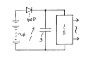
- a voltage booster with an output switch (140) and a smoothing capacitor (3) applies a boosted DC voltage to a power converter for driving a switched reluctance motor.
- the output switch (140) is connected in series to the power converter (2) and a DC power source (4).
- the smoothing capacitor (3) is connected in parallel to the power converter (2).
- the power converter (2) has a predetermined transient period (Pt) when the power converter (2) starts to output a freewheeling current, which is a recovery current generated by a residual magnetic energy accumulated in the switched reluctance motor.
- the output switch (140) is opened in the transient period (Pt) in order to accumulate the residual magnetic energy of the switched reluctance motor (60) in the smoothing capacitor (3). Accordingly, freewheeling currents of the switched reluctance motor can be decreased quickly. Moreover, phase currents can rise up quickly, because the DC link voltage applied to the power converter is increased.
- the output switch consists of an output switch of a chopper type DC-to-DC converter for boosting the DC power source.
- the voltage booster becomes simple.
- Figure 1 is a circuit topology configuration showing a conventional single chopper type DC-to-DC boost converter for driving a motor-driving circuit.
- Figure 2 is a circuit topology configuration showing a conventional dual chopper type DC-to-DC boost converter for driving a motor-driving circuit.
- Figure 3 is a circuit topology configuration showing a motor-driving-apparatus of a first embodiment.
- Figure 4 is a circuit topology configuration showing a series stage of the boost converter shown in Figure 3.
- Figure 5 is a circuit topology configuration showing a short-circuited stage of the boost converter shown in Figure 3.
- Figure 6 is a circuit topology configuration showing a parallel stage of the boost converter shown in Figure 3.
- Figure 7 is a circuit topology configuration showing an open stage of the boost converter shown in Figure 3.
- Figure 8 is a circuit topology configuration showing one partial short-circuited stage of the boost converter shown in Figure 3.
- Figure 9 is a circuit topology configuration showing another partial short-circuited stage of the boost converter shown in Figure 3.
- Figure 10 is a timing chart showing a DC link voltage applied by the boost converter shown in Figure 3.
- Figure 11 is a timing chart showing a DC link voltage applied by the conventional boost converter shown in Figure 1.
- Figure 12 is a timing chart showing a DC link voltage applied by the conventional series-parallel connection circuit shown in Figure 2.
- Figure 13 is a circuit topology configuration showing a motor-driving-apparatus of a second embodiment.
- Figure 14 is a circuit topology configuration showing a high voltage mode (A) of the second embodiment.
- Figure 15 is a circuit topology configuration showing a low voltage mode (B) of the second embodiment.
- Figure 16 is a circuit topology configuration showing a first middle voltage mode (C) of the second embodiment.
- Figure 17 is a circuit topology configuration showing a second middle voltage mode (D) of the second embodiment.
- Figure 18 is a timing chart showing waveforms of gate voltages and the DC link voltage Vx in the second embodiment shown in Figure 13.
- Figure 19 is a timing chart showing waveforms of gate voltages and the DC link voltage Vx in the second embodiment shown in Figure 13.
- Figure 20 is a circuit topology configuration showing a motor-driving-apparatus of a third embodiment.
- Figure 21 is a schematic cross-section of a Hendershot type five-phase switched reluctance motor employed in the third embodiment.
- Figure 22 is a schematic cross-section of a Hendershot type five-phase switched reluctance motor employed in the third embodiment.
- Figure 23 is a schematic cross-section of a Hendershot type five-phase switched reluctance motor employed in the third embodiment.
- Figure 24 is a schematic cross-section of a Hendershot type five-phase switched reluctance motor employed in the third embodiment.
- Figure 25 is a schematic cross-section of a Hendershot type five-phase switched reluctance motor employed in the third embodiment.
- Figure 26 is a timing chart of the third embodiment.
- Figure 27 is a timing chart showing a fourth embodiment.
- Figure 28 is a circuit topology configuration showing a first arranged embodiment of the fourth embodiment.
- Figure 29 is a circuit topology configuration showing a second arranged embodiment of the fourth embodiment.
- Figure 30 is a circuit topology configuration showing a fifth embodiment.
- Figure 31 is a timing chart showing a strong lighting mode of the fifth embodiment.
- Figure 32 is a timing chart showing a normal lighting mode of the fifth embodiment.
- Figure 33 is a timing chart showing a low lighting mode of the fifth embodiment.
- Figure 34 is a circuit topology configuration showing a sixth embodiment.
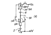
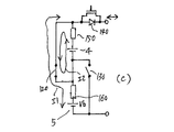
- FIG. 3 shows a circuit topology of a motor-driving apparatus of the first embodiment.
- the motor-driving apparatus drives a motor 60, for example a switched reluctance motor-generator (SRMG).
- the motor-driving apparatus consists of a boost chopper type DC-to-DC converter 1, a motor-driving circuit 2 and a smoothing capacitor 3.
- the motor-driving circuit 2 consists of a power converter for driving the switched reluctance motor 60.
- Motor-driving circuit 2 can consist of an inverter for driving a synchronous motor or an asynchronous motor.
- the boost chopper type DC-to-DC converter 1 called the voltage booster, boosts battery voltages Vb of two batteries 4 and 5, and applies a DC link voltage Vx to power converter 2 and smoothing capacitor 3.
- Power converter 2 applies a multi-phase voltage to a motor 60.
- Voltage booster 1 with two boost choppers consists of a series switch 110, parallel switches 120 and 130 and an output switch 140.
- the voltage booster 1, which is the DC-to-DC converter 1 has a first reactor 150 and a second reactor 160.
- the first boost chopper consists of the reactor 150 and the switches 110, 120 and 140.
- the second boost chopper consists of the reactor 160 and the switch 110, 130 and 140.
- voltage booster 1 can employ a diode instead of the output switch 140, if the motor 60 is not driven as a generator.
- Voltage booster 1 outputs a DC link voltage Vx to power converter 2 and smoothing capacitor 3 via a pair of DC link lines 6 and 7 consisting of a high potential line 6 and a low potential line 7.
- Figures 4-9 show six connection states of the voltage booster 1.
- Batteries 4 and 5 have 125V each.
- Figure 4 shows a series connection state A. In the state A, parallel switches 120 and 130 are turned off, and series switch 110 is turned on. Output switch 140 should be turned on. A diode can be employed as the output switch 140, if voltage booster 1 is one-way type.
- DC link voltage Vx becomes 250 V or more than 250V, because reactors 150 and 160 connected in series to each other have magnetic energies and output voltages each.
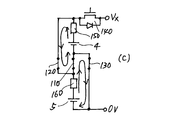
- Figure 5 shows a full short-circuit state C.
- three switches 110, 120 and 130 are turned on.
- the output switch 140 is turned off, if the output switch 140 is a transistor instead of a diode.
- Currents of the reactors 150 and 160 are increased, and reactors 150 and 160 accumulate magnetic energies.
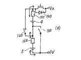
- Figure 6 shows a parallel connection state B.
- parallel switches 120 and 130 are turned on, and series switch 110 is turned off.
- Output switch 140 should be turned on, if the output switch 140 is a transistor instead of a diode.
- DC link voltage Vx becomes 125V or more than 125V, because reactors 150 and 160 connected in parallel to each other has magnetic energies and has voltages each.
- Figure 7 shows a full-opened connection state D. In the state D, three switches 110, 120 and 130 are turned off. By the turning-off of three switches 110, 120 and 130 and the output switch 140, the battery voltage is separated safely.
- Figure 8 shows a first half-short-circuit connection state E. In the state E, parallel switch 120 and series switch 110 are turned on, and parallel switch 130 is turned off. Output switch 140 can be turned on. DC link voltage Vx becomes 125V or more than 125V by reactor 160 and battery 5.
- Reactor 150 accumulates magnetic energy. It is important that magnetizing of reactor 150 and demagnetizing of reactor 160 are executed simultaneously. Moreover, a freewheeling current of battery 4 and a boost current of battery 5 have opposite directions to each other in parallel switch 120, when the boost converter outputs the boost current. As the result, the resistive power loss of parallel switch 120 is reduced largely.
- Figure 9 shows a second half-short-circuit connection state F.
- state F parallel switch 130 and series switch 110 are turned on, and parallel switch 120 is turned off.
- DC link voltage Vx becomes 125V or more than 125V by reactor 150 and battery 5.
- Reactor 160 accumulates magnetic energy. It is important that magnetizing of reactor 160 and demagnetizing of reactor 150 are executed simultaneously.
- a freewheeling current of battery 5 and a boost current of battery 4 have opposite directions to each other in parallel switch 130, when the boost converter outputs the current. As the result, the resistive power loss of parallel switch 130 is reduced largely.
- a plurality of the states selected in the states A-F can be executed alternately or in turn for operating a selected one of boost modes.
- the states A and C are operated alternately with a predetermined career frequency.
- a boost ratio is controlled by changing a period ratio, a PWM duty ratio, between the states A and C.
- the states B and C are operated alternately with a predetermined career frequency.
- the boost ratio is controlled by changing a period ratio, the PWM duty ratio, between the states B and C.
- the states E, A, F and A are operated in turn with a predetermined career frequency.
- the states E, B, F and B are operated in turn with a predetermined career frequency.
- the current ripple is reduced, because one reactor accumulates the magnetic energy, and another reactor consumes the magnetic energy.
- the boost ratio can be controlled by changing the PWM duty ratio of parallel switches 120 and 130.
- Figure 10 is a timing chart showing DC link voltage Vx changed by changing the modes or the states.
- DC link voltage Vx becomes 125V.
- T3 employing the series connection state A
- the DC link voltage Vx is 250V.
- T2 between the periods T1 and T3
- the low boost mode is employed.
- DC link voltage Vx becomes an intermediate value between 125V and 250V.
- the high boost mode is employed.
- DC link voltage Vx becomes more than 250V.
- FIG 11 is a timing chart showing DC link voltage Vx applied by the conventional boost converter shown in Figure 1.
- Figure 12 is a timing chart showing the voltage Vx applied by the conventional series-parallel-changing circuit. Consequently, the voltage booster 1 shown in Figure 3 can apply either one of two constant values 125V and 250V of the DC link voltage Vx without switching of voltage booster 1. Furthermore, voltage booster 1 can change DC link voltage Vx smoothly and widely. Switching loss and current ripple of the voltage booster 1 are reduced by means of selecting the best boost mode of the voltage booster 1 in accordance with a value of DC link voltage Vx. For example, resistive power loss of the boost converter becomes 25% in the parallel state B, because the boost currents flow in parallel.
- FIG. 13 shows a circuit topology of a motor-driving apparatus of the second embodiment.
- the motor-driving apparatus drives a switched reluctance motor-generator (SRMG) 60.
- the motor-driving apparatus consists of a boost chopper type DC-to-DC converter 1, a motor-driving circuit 2 and a smoothing capacitor 3.
- the motor-driving circuit 2 consists of a power converter for driving the switched reluctance motor 60.
- Motor-driving circuit 2 can consist of an inverter for driving a synchronous motor or an asynchronous motor.
- the boost chopper type DC-to-DC converter 1, the voltage booster 1, can boost each battery voltage Vb of batteries 4 and 5, and applies a boosted DC link voltage Vx to power converter 2 and smoothing capacitor 3.
- Power converter 2 applies a five-phase voltage to five-phase SRMG 60.
- Voltage booster 1 has parallel switches 120 and 130, an output switch 140 and reactors 150 and 160.
- the reactors 150 and 160 have a predetermined value of inductance each.
- Reactors 150 and 160, batteries 4 and 5 and the output switch 140 are connected in series to each other.
- the parallel switch 120 is connected in parallel to a pair of the battery 4 and the reactor 150 connected in series.
- the parallel switch 130 is connected in parallel to a pair of the battery 5 and the reactor 160 connected in series.
- the output switch 140 is connected to a positive DC terminal of the motor-driving circuit 2 via a high potential DC link 6.
- Reactor 160 is connected to a negative DC terminal of the motor-driving circuit 2 via a low potential DC link 7.
- voltage booster 1 are connected to motor-driving circuit 2 via a high potential DC link 6 and a low potential DC link 7.
- a controller 70 controls voltage booster 1 and motor-driving circuit 2.
- FIG. 14 shows a high voltage mode (A). Parallel switches 120 and 130 are opened. Voltage booster 1 outputs 250V + V150 + V160. Reactor 150 has a voltage V150. Reactor 160 has a voltage V160. The output switch 140 is turned on. Figure 15 shows a low voltage mode (B). Parallel switches 120 and 130 are closed. Voltage booster 1 outputs 0V. The output switch 140 is turned off.
- Figure 16 shows a first middle voltage mode (C).
- Parallel switch 120 is closed.
- Parallel switch 130 is opened.
- the output switch 140 is turned on.
- Battery 5 and reactor 160 output 125V + V160.
- Reactor 150 accumulates a magnetic energy. It is important that a current I1 flowing through battery 5 and reactor 160 has an opposite direction to a magnetizing current I2 flowing through battery 4 and reactor 150, when voltage booster 1 supplies a motor current to motor-driving circuit 2. Accordingly, a current difference I1-I2 passing through parallel switch 120 is decreased.
- FIG 17 shows a second middle voltage mode (D).
- Parallel switch 130 is closed.
- Parallel switch 120 is opened.
- the output switch 140 is turned on.
- Battery 4 and reactor 150 output 125V + V150.
- Reactor 160 accumulates a magnetic energy. It is important that a current I2 flowing through battery 4 and reactor 150 has an opposite direction to a magnetizing current I1 flowing through battery 5 and reactor 160, when voltage booster 1 supplies a motor current to motor-driving circuit 2. Accordingly, a current difference I1-I2 passing through parallel switch 130 is decreased.
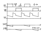
- Figure 18 is a timing chart showing an alternative switching mode for outputting a low average value of boosted voltage Vx.
- a gate voltage VA is applied to a gate of parallel switch 120.
- a gate voltage VB is applied to a gate of parallel switch 130.
- the gate voltage VA and the gate voltage VB are applied alternately. Accordingly, the DC link voltage Vx across the power converter 2 becomes small relatively and has low ripples relatively.
- switching power losses of the parallel switches 120 and 130 becomes very small, because a current I120 of the parallel switch 120 and a current I130 of the parallel switch 130 become very small in comparison with an overlapped switching mode shown in Figure 19.
- Figure 19 is a timing chart showing the overlapped switching mode for outputting a high voltage. Turned-on periods of two parallel switches 120 and 130 are overlapped. Both of gate voltages VA and VB are applied for same periods. Accordingly, the DC link voltage Vx has become large relatively and has high ripples relatively. Consequently, amplitude and the ripples of the boosted voltage Vx can be controlled by means of controlling a phase difference and PWM duty ratio of gate voltages VA and VB, which are PWM-switched.
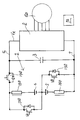
- Figure 20 shows a circuit topology of a motor-driving apparatus of the third embodiment.
- the motor-driving circuit 2 consists of a five-phase power converter for driving the Hendershot type five-phase SRMG. This five-phase power converter is explained in PCT/JP2010/006674 applied by the inventor.
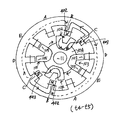
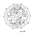
- Figures 21-25 are schematic configurations for showing five angular positions of the five-phase SRM with ten stator poles and four U-shaped rotor pole pairs.
- the five-phase SRM has two sets of five phase windings 401-405 constituting a stator winding. Each of five phase windings 401-405 is wound on each of stator poles A-E of a stator 201 in turn.
- Five-phase power converter 2 consists of six transistors 201-206 and six freewheeling diodes 301-306. Transistors can be employed instead of the freewheeling diodes 301-306.
- the upper transistors 201, 203 and 205 connect the high potential DC link line 6 and the phase windings 401, 403 and 405 respectively.
- the lower transistors 202, 204 and 206 connect the low potential DC link line 7 and the phase windings 402, 404 and 405 respectively.
- the other ends of phase windings 401-405 are connected to a neutral line N. Accordingly, five phase windings 401-405 has a star configuration connection. It is important that the Hendershot type five-phase SRM can be driven by the simple five-phase power converter with star configuration connection.
- the lower freewheeling diodes 301, 303 and 305 are connected to one ends of phase windings 401, 403 and 405 respectively.
- the upper freewheeling diodes 302, 304 and 306 are connected to one ends of phase windings 402, 404 and 406 respectively.
- Each of transistors switched synchronously can be connected to each of freewheeling diodes 301-306 in parallel due to reduce the known diode voltage drop.
- Voltage booster 1 shown in Figure 13 applies boosted DC link voltage Vx to power converter 2.
- Five-phase 10/8 SRM shown in Figures 21-25 has a stator 9 and a rotor core 10.
- the stator 9 has two sets of five stator poles A-E connected magnetically to each other with a cylinder-shaped stator core back 90.
- the rotor core 10 has four U-shaped rotor pole cores 101-104 fixed on an outer circumferential surface of a nonmagnetic cylinder portion 10A press-fixed on an axis 11.
- Each of U-shaped rotor pole cores 101-104 having two rotor poles 105 each are disposed with a constant circumferential pitch on the outer surface of the rotor core back 10A. Arrangement of ten rotor poles 105 is same as it of the Hendershot's five-phase 10/8 SRM.
- Rotor 10 has two kinds of circumferential rotor pole gaps, which are four narrow gaps and four wide gaps.
- the narrow gap and the wide gap are disposed alternately between adjacent two rotor poles 105.
- a circumferential width of the wide rotor pole gap between adjacent two U-shaped rotor poles is about 150% of a circumferential width of the narrow rotor pole gap between adjacent two rotor poles of one U-shaped rotor pole.
- Each angular position of rotor 10 at each time t1, t2, t3, t4 and t5 is shown in Figures 11-15.
- transistors 205 and 204 are turned on in a period from t3 to t4.
- a phase currents Ied is supplied to the phase winding 405 and 404.
- transistors 203 and 202 are turned on in a period from t4 to t5.
- a phase currents Icb is supplied to the phase windings 403 and 402.
- transistors 201 and 206 are turned on in a period from t5 to t1.
- a phase currents Iae is supplied to the phase windings 401 and 405.
- transistors 203 and 204 are turned on in a period from t1 to t2.
- a phase current Icd is supplied to the phase windings 403 and 404.
- transistors 201 and 202 are turned on in a period from t2 to t3.
- a phase currents Iab is supplied to the phase winding 401 and 402. It should be considered that the phase current Iae in the period from t5 to t1 flows toward an opposite direction to the phase current Ied in the period from t3 to t4.
- one of upper transistors 201, 203 and 205 and one of lower transistors 202, 204 and 206 are turned on in the same period and turned off in the same period.
- an electric potential of the neutral line N is not changed by means of the turning-on and the turning-off of the two transistors at one time. It means that the single-switch-per-phase power converter 2 does not need well-known two split capacitors which are required in a conventional split voltage type converter with the single-switch-per-phase topology.
- dotted lines show the magnetic flux flowing in long paths of the stator core back 90.
- Real lines show the magnetic flux flowing in short paths. Iron loss of the core back 90 is reduced by the magnetic flux in the long paths of stator core back 90.
- Figure 26 is a timing chart showing five phase voltages Va, Vb, Vc, Vd and Ve applied to five phase windings 401-405 of five-phase SRM.
- the phase voltage Va is applied to phase winding 401.
- the phase voltage Vb is applied to phase winding 402.
- the phase voltage Vc is applied to phase winding 403.
- the phase voltage Vd is applied to phase winding 404.
- the phase voltage Ve is applied to phase winding 405.
- Each of the phase voltages Va, Vb, Vc, Vd and Ve is increased in each transient period Pt consisting of current-increasing periods and current-decreasing periods.
- One constant current period is arranged between one current-increasing period and one current-decreasing period as shown in Figure 26.
- Each of the phase voltages Va, Vb, Vc, Vd and Ve is increased in each transient period Pt by means of increasing the DC link voltage Vx.
- each phase current Iae, Icb, Icd, Iae and Ied can rise up quickly and can fall down quickly.
- the voltage booster 1 increases the DC link voltage Vx in the transient periods Pt. As the result, a motor torque is increased largely.
- Increasing of the DC link voltage Vx is executed by boosting operation of the boost DC/DC converter 1 explained above.
- Figure 27 is a timing chart showing a part of Figure 26.
- Figure 27 shows waveforms of an inductance L401 of the phase winding 401, an inductance L405 of the phase winding 405, an inductance L403 of the phase winding 403 and an inductance L404 of the phase winding 404.
- Figure 27 shows phase currents Iae, Iab, Icb and Icd and the DC link voltage Vx.
- the transient period Pt in which the phase current increases or decreases quickly, is formed from a time point t5 to a time point t51, from a time point t1 to a time point t11 and from a time point t2 to a time point t21.
- increased phase currents rise up quickly by means of increasing the DC link voltage Vx.
- decreased phase currents which are freewheeling currents, fall down quickly by means of decreasing the DC link voltage Vx.
- the DC link voltage Vx is increased in the transient period Pt by means of the opening of the output switch 140 of voltage booster 1.
- transistors 203 and 202 are opened, and transistors 201 and 206 are closed, in the transient period Pt from t5 to t51.
- the output switch 140 is closed in the transient period Pt from t5 to t51.
- the freewheeling current Icb charges the smoothing capacitor 3 quickly in the transient period Pt.
- the phase current Iae rises up quickly, and the phase current Icb falls down quickly, by means of the increasing of the DC link voltage Vx across the smoothing capacitor 3 in the transient period Pt from t5 to t51.
- phase current Iae falls down quickly, and the phase current Icd rises up quickly, by means of the closing of the output switch 140 in the transient period Pt from t1 to t11.
- phase current Icd falls down quickly, and the phase current Iab rises up quickly, by means of the closing of the output switch 140 in the transient period Pt from t2 to t21.
- a waveform of the DC link voltage Vx is shown in Figure 27.
- the DC link voltage Vx is increased quickly by the freewheeling current in an initial period of the transient period Pt. Then, the DC link voltage Vx is increased quickly by the freewheeling current in an initial period of the transient period Pt. Then, the DC link voltage Vx is decreased. Then, amplitude of the DC link voltage Vx becomes constant by means of PWM-switching of the transistors of the power converter 2 in a constant-current-period Tb.
- the amplitude of the DC link voltage Vx in a freewheeling period Tf is larger than the amplitude of the DC link voltage Vx in the constant-current-period Tb.
- the output switch 140 of the voltage booster 1 should be turned on, after the DC link voltage Vx is mostly equal to an output voltage of the voltage booster 1.
- the closed transistors of the power converter 1 are PWM-switched in order to keep the phase current constant.
- the phase current is increased quickly when the inductance of the phase winding is in a large range, and the phase current is decreased quickly when the inductance of the phase winding is in a small range, as known well.
- voltage booster 1 does not need that the parallel switches 120 and 130 are switched with the PWM-switching method. However, it is desirable to operate the PWM-switching of the parallel switches 120 and 130 in accordance with a rotating speed of the SRM. For example, the output voltage should be increased in a high rotation speed range of the SRM.
- An important feature of this embodiment is that the output switch 140 of the voltage booster 1 is opened in the transient period Pt while the freewheeling current of each phase is energized. Accordingly, the freewheeling current of the power converter 2 charges the smoothing capacitor 3 instead of the voltage booster 1.
- the DC link voltage Vx is increased by means of charging the smoothing capacitor 3.
- the output switch 140 should be turned on again, after the DC link voltage Vx becomes equal or less than the output voltage of voltage booster 1.
- the voltage booster 1 consists of only a pair of the output switch 140 and the smoothing capacitor 3.
- the output switch 140 connects one battery 4 to the high potential DC link line 6.
- the output switch 140 is opened in the transient period Pt when the freewheeling current flows out from the power converter 2.
- the freewheeling current of the power converter 2 charges the smoothing capacitor 3.
- the DC link voltage Vx is increased in the transient period Pt. As the result, the phase current can rise up quickly, and the phase current can fall down quickly.
- the voltage booster 1 consists of only a pair of the output diode 140A and the smoothing capacitor 3.
- the output diode 140A connects the battery 4 to the high potential DC link line 6.
- the switched reluctance motor (not illustrated) are not operated as the generator, but are operated as the motor.
- FIG. 30 shows a circuit topology of a sun cell power generator with a voltage booster 1 and three sun cells 4A, 4B and 4C.
- Each of the sun cells 4A, 4B and 4C is a DC power sources for transforming a sun light to a DC voltage.
- the sun cell power generator has a first generator block A, a second generator block B, a third generator block C, an output switch 140 and a smoothing capacitor 3.
- the output switch 140 can consist of only one diode.
- the first generator block A consists of sun cell 4A, a reactor 150A and a parallel switch 120A.
- the second generator block B consists of sun cell 4B, reactor 150B and a parallel switch 120B.
- the third generator block C consists of sun cell 4C, a reactor 150C and a parallel switch 120C.
- voltage booster 1 shown in Figure 30 is essentially same as the voltage booster 1 shown in Figure 13 except a fact that one more pair of the reactor and the parallel switch is added.
- the sun cells 4A, 4B and 4C are essentially same as the batteries 4 and 5 shown in Figure 13.
- Parallel switch 120A is connected in parallel to a pair of sun cell 4A and reactor 150A, which are connected in series.
- Parallel switch 120B is connected in parallel to a pair of sun cell 4B and reactor 150B, which are connected in series.
- Parallel switch 120C is connected in parallel to a pair of sun cell 4C and reactor 150C, which are connected in series.
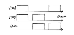
- Figures 31-33 are timing charts showing gate voltages of parallel switches 120A, 120B and 120C.
- Figure 31 shows a strong lighting mode in a time when sun shine is strong.
- the parallel switches 120A, 120B and 120C are turned on in turn. Accordingly, a boost ration of the voltage booster 1 becomes relatively low.
- Figure 32 shows a medium lighting mode in a time when sun shine is normal.
- each two of the parallel switches 120A; 120B and 120C are turned on in turn. Accordingly, a boost ratio of the voltage booster 1 becomes middle relatively.
- Figure 33 shows a low lighting mode in a time when sun shine is low. all of the parallel switches 120A, 120B and 120C are turned simultaneously.
- Each PWM-ratio of parallel switches 120A, 120B and 120C are changed in accordance with the strength of the sun light. After all, the changing voltage of the sun cells 4A, 4B and 4C are compensated with the voltage booster 1. It is important that the current Is, which is a magnetizing current of the reactor, when the parallel switch is turned on, has the opposite flow direction in comparison with the generation current of the sun cell. Consequently, PWM-switched parallel switches 120A, 120B and 120C have a small power loss each.
- electrical double-layer capacitors are employed instead of the sun cells 4A, 4B and 4C shown in Figure 30.
- the electrical double-layer capacitors have a weak point that a capacitor voltage changes largely in accordance with a value of the accumulated energy.
- the voltage booster 1 shown in Figure 30 compensates the voltage change without a large power loss of the voltage boosting.
- more than three of generator blocks can be connected in series to each other.
- FIG. 34 shows a circuit topology of a motor-driving apparatus with a voltage booster 1.
- Voltage booster 1 shown in Figure 34 is essentially same as the voltage booster 1 shown in Figure 13.
- voltage booster 1 shown in Figure 34 has a common soft magnetic core on which coils of reactors 150 and 160 are wound. Accordingly, the two coils of reactors 150 and 160 constitute a transformer, too.
Landscapes
- Engineering & Computer Science (AREA)
- Power Engineering (AREA)
- Dc-Dc Converters (AREA)
Abstract
L'objet de l'invention est de fournir un survolteur capable d'augmenter une tension de sortie d'une source de tension de courant continu. Deux paires de réacteurs et de sources de courant continu sont connectées en série l'une à l'autre. Chaque paire est court-circuitée par chaque commutateur parallèle. Une perte de puissance du commutateur parallèle commutée MID est diminuée. Un commutateur en série destiné à connecter deux paires peut être fourni. Dans un autre cas, un survolteur destiné à appliquer une tension d'amplification sur un convertisseur de secteur entraînant un moteur à réluctance commuté est constitué d'un commutateur de sortie et d'un condensateur de filtrage afin d'accumuler une énergie magnétique résiduelle du moteur à réluctance commuté. L'élévation et la chute des courants de phase du moteur à réluctance commuté deviennent rapides.
Priority Applications (1)
| Application Number | Priority Date | Filing Date | Title |
|---|---|---|---|
| PCT/JP2011/002259 WO2012143968A1 (fr) | 2011-04-18 | 2011-04-18 | Survolteur |
Applications Claiming Priority (1)
| Application Number | Priority Date | Filing Date | Title |
|---|---|---|---|
| PCT/JP2011/002259 WO2012143968A1 (fr) | 2011-04-18 | 2011-04-18 | Survolteur |
Publications (1)
| Publication Number | Publication Date |
|---|---|
| WO2012143968A1 true WO2012143968A1 (fr) | 2012-10-26 |
Family
ID=47041126
Family Applications (1)
| Application Number | Title | Priority Date | Filing Date |
|---|---|---|---|
| PCT/JP2011/002259 Ceased WO2012143968A1 (fr) | 2011-04-18 | 2011-04-18 | Survolteur |
Country Status (1)
| Country | Link |
|---|---|
| WO (1) | WO2012143968A1 (fr) |
Cited By (4)
| Publication number | Priority date | Publication date | Assignee | Title |
|---|---|---|---|---|
| JP5624176B1 (ja) * | 2013-06-13 | 2014-11-12 | 株式会社豊田中央研究所 | 電源システム |
| CN104216453A (zh) * | 2013-07-11 | 2014-12-17 | 马鞍山恒瑞测量设备有限公司 | 小电流高精度可变高压输出装置 |
| JP2016178812A (ja) * | 2015-03-20 | 2016-10-06 | 株式会社豊田中央研究所 | 電源システム |
| DE102015210272A1 (de) * | 2015-06-03 | 2016-12-08 | Bayerische Motoren Werke Aktiengesellschaft | Elektrische Energieversorgungsschaltung für Kraftfahrzeuge |
Citations (3)
| Publication number | Priority date | Publication date | Assignee | Title |
|---|---|---|---|---|
| JPH11113283A (ja) * | 1997-09-30 | 1999-04-23 | Toshiba Corp | モータの駆動装置 |
| JP2008005625A (ja) * | 2006-06-22 | 2008-01-10 | Toyota Motor Corp | 電圧変換装置およびそれを備えた車両 |
| JP2010193700A (ja) * | 2008-08-25 | 2010-09-02 | Suri-Ai:Kk | スイッチドリラクタンスモータ装置 |
-
2011
- 2011-04-18 WO PCT/JP2011/002259 patent/WO2012143968A1/fr not_active Ceased
Patent Citations (3)
| Publication number | Priority date | Publication date | Assignee | Title |
|---|---|---|---|---|
| JPH11113283A (ja) * | 1997-09-30 | 1999-04-23 | Toshiba Corp | モータの駆動装置 |
| JP2008005625A (ja) * | 2006-06-22 | 2008-01-10 | Toyota Motor Corp | 電圧変換装置およびそれを備えた車両 |
| JP2010193700A (ja) * | 2008-08-25 | 2010-09-02 | Suri-Ai:Kk | スイッチドリラクタンスモータ装置 |
Cited By (5)
| Publication number | Priority date | Publication date | Assignee | Title |
|---|---|---|---|---|
| JP5624176B1 (ja) * | 2013-06-13 | 2014-11-12 | 株式会社豊田中央研究所 | 電源システム |
| WO2014200049A1 (fr) * | 2013-06-13 | 2014-12-18 | トヨタ自動車株式会社 | Système d'alimentation électrique |
| CN104216453A (zh) * | 2013-07-11 | 2014-12-17 | 马鞍山恒瑞测量设备有限公司 | 小电流高精度可变高压输出装置 |
| JP2016178812A (ja) * | 2015-03-20 | 2016-10-06 | 株式会社豊田中央研究所 | 電源システム |
| DE102015210272A1 (de) * | 2015-06-03 | 2016-12-08 | Bayerische Motoren Werke Aktiengesellschaft | Elektrische Energieversorgungsschaltung für Kraftfahrzeuge |
Similar Documents
| Publication | Publication Date | Title |
|---|---|---|
| US7151364B2 (en) | DC/DC converter and program | |
| US20220077709A1 (en) | Power battery charging method, motor control circuit, and vehicle | |
| JP4274364B2 (ja) | Dc−dcコンバータ | |
| JP5686131B2 (ja) | 電力変換装置 | |
| WO2011092774A9 (fr) | Convertisseur élévateur continu-continu et convertisseur électrique alimenté par celui-ci | |
| WO2012063385A1 (fr) | Appareil de commande de moteur capable de charger une batterie de véhicule | |
| EP1717946B1 (fr) | Générateur à réluctance commutée | |
| KR100991923B1 (ko) | 스위치드 릴럭턴스 모터의 구동장치를 위한 패시브 컨버터 | |
| US9866129B2 (en) | Power conversion device including primary inverter, transformer, secondary converter, and controller | |
| US7049786B1 (en) | Unipolar drive topology for permanent magnet brushless DC motors and switched reluctance motors | |
| KR20230119441A (ko) | 모터 구동 시스템을 이용한 차량용 배터리 충전 시스템 | |
| US9866135B2 (en) | Power conversion device including primary inverter, transformer, secondary converter | |
| EP3121952B1 (fr) | Moteur à réluctance commutée avec circuit de commande et procédé pour faire fonctionner un moteur à réluctance commutée | |
| KR20230013551A (ko) | 모터 구동 시스템을 이용한 차량용 배터리 충전 시스템 | |
| US20150162841A1 (en) | Electric power conversion device | |
| KR20230000334A (ko) | 모터 구동 시스템을 이용한 차량용 배터리 충전 시스템 | |
| WO2011004546A1 (fr) | Appareil de moteur à réluctance | |
| EP4108507A1 (fr) | Système de charge de batterie de véhicule à l'aide d'un système de commande de moteur | |
| WO2012143968A1 (fr) | Survolteur | |
| US10173534B2 (en) | Variable voltage converter control in vehicles | |
| WO2012053027A1 (fr) | Convertisseur continu-continu d'amplification et moteur à réluctance commuté alimenté au moyen de celui-ci | |
| KR102246884B1 (ko) | 전력 변환 회로 | |
| Pittermann et al. | Converters for switched reluctance motor-topology comparison | |
| US20140361619A1 (en) | Power device | |
| Wang et al. | High frequency bidirectional isolated matrix converter for AC-motor drives with model predictive control |
Legal Events
| Date | Code | Title | Description |
|---|---|---|---|
| 121 | Ep: the epo has been informed by wipo that ep was designated in this application |
Ref document number: 11863735 Country of ref document: EP Kind code of ref document: A1 |
|
| NENP | Non-entry into the national phase |
Ref country code: DE |
|
| 32PN | Ep: public notification in the ep bulletin as address of the adressee cannot be established |
Free format text: NOTING OF LOSS OF RIGHTS PURSUANT TO RULE 112(1) EPC |
|
| 122 | Ep: pct application non-entry in european phase |
Ref document number: 11863735 Country of ref document: EP Kind code of ref document: A1 |