WO2012144163A1 - Dcdcコンバータ及びその制御方法 - Google Patents
Dcdcコンバータ及びその制御方法 Download PDFInfo
- Publication number
- WO2012144163A1 WO2012144163A1 PCT/JP2012/002519 JP2012002519W WO2012144163A1 WO 2012144163 A1 WO2012144163 A1 WO 2012144163A1 JP 2012002519 W JP2012002519 W JP 2012002519W WO 2012144163 A1 WO2012144163 A1 WO 2012144163A1
- Authority
- WO
- WIPO (PCT)
- Prior art keywords
- signal
- level
- control circuit
- switch element
- time
- Prior art date
- Legal status (The legal status is an assumption and is not a legal conclusion. Google has not performed a legal analysis and makes no representation as to the accuracy of the status listed.)
- Ceased
Links
Images




Classifications
-
- H—ELECTRICITY
- H02—GENERATION; CONVERSION OR DISTRIBUTION OF ELECTRIC POWER
- H02M—APPARATUS FOR CONVERSION BETWEEN AC AND AC, BETWEEN AC AND DC, OR BETWEEN DC AND DC, AND FOR USE WITH MAINS OR SIMILAR POWER SUPPLY SYSTEMS; CONVERSION OF DC OR AC INPUT POWER INTO SURGE OUTPUT POWER; CONTROL OR REGULATION THEREOF
- H02M3/00—Conversion of DC power input into DC power output
- H02M3/02—Conversion of DC power input into DC power output without intermediate conversion into AC
- H02M3/04—Conversion of DC power input into DC power output without intermediate conversion into AC by static converters
- H02M3/10—Conversion of DC power input into DC power output without intermediate conversion into AC by static converters using discharge tubes with control electrode or semiconductor devices with control electrode
- H02M3/145—Conversion of DC power input into DC power output without intermediate conversion into AC by static converters using discharge tubes with control electrode or semiconductor devices with control electrode using devices of a triode or transistor type requiring continuous application of a control signal
- H02M3/155—Conversion of DC power input into DC power output without intermediate conversion into AC by static converters using discharge tubes with control electrode or semiconductor devices with control electrode using devices of a triode or transistor type requiring continuous application of a control signal using semiconductor devices only
- H02M3/156—Conversion of DC power input into DC power output without intermediate conversion into AC by static converters using discharge tubes with control electrode or semiconductor devices with control electrode using devices of a triode or transistor type requiring continuous application of a control signal using semiconductor devices only with automatic control of output voltage or current, e.g. switching regulators
- H02M3/158—Conversion of DC power input into DC power output without intermediate conversion into AC by static converters using discharge tubes with control electrode or semiconductor devices with control electrode using devices of a triode or transistor type requiring continuous application of a control signal using semiconductor devices only with automatic control of output voltage or current, e.g. switching regulators including plural semiconductor devices as final control devices for a single load
- H02M3/1588—Conversion of DC power input into DC power output without intermediate conversion into AC by static converters using discharge tubes with control electrode or semiconductor devices with control electrode using devices of a triode or transistor type requiring continuous application of a control signal using semiconductor devices only with automatic control of output voltage or current, e.g. switching regulators including plural semiconductor devices as final control devices for a single load comprising at least one synchronous rectifier element
-
- H—ELECTRICITY
- H02—GENERATION; CONVERSION OR DISTRIBUTION OF ELECTRIC POWER
- H02M—APPARATUS FOR CONVERSION BETWEEN AC AND AC, BETWEEN AC AND DC, OR BETWEEN DC AND DC, AND FOR USE WITH MAINS OR SIMILAR POWER SUPPLY SYSTEMS; CONVERSION OF DC OR AC INPUT POWER INTO SURGE OUTPUT POWER; CONTROL OR REGULATION THEREOF
- H02M1/00—Details of apparatus for conversion
- H02M1/32—Means for protecting converters other than automatic disconnection
-
- H—ELECTRICITY
- H02—GENERATION; CONVERSION OR DISTRIBUTION OF ELECTRIC POWER
- H02M—APPARATUS FOR CONVERSION BETWEEN AC AND AC, BETWEEN AC AND DC, OR BETWEEN DC AND DC, AND FOR USE WITH MAINS OR SIMILAR POWER SUPPLY SYSTEMS; CONVERSION OF DC OR AC INPUT POWER INTO SURGE OUTPUT POWER; CONTROL OR REGULATION THEREOF
- H02M1/00—Details of apparatus for conversion
- H02M1/0003—Details of control, feedback or regulation circuits
-
- H—ELECTRICITY
- H02—GENERATION; CONVERSION OR DISTRIBUTION OF ELECTRIC POWER
- H02M—APPARATUS FOR CONVERSION BETWEEN AC AND AC, BETWEEN AC AND DC, OR BETWEEN DC AND DC, AND FOR USE WITH MAINS OR SIMILAR POWER SUPPLY SYSTEMS; CONVERSION OF DC OR AC INPUT POWER INTO SURGE OUTPUT POWER; CONTROL OR REGULATION THEREOF
- H02M1/00—Details of apparatus for conversion
- H02M1/0003—Details of control, feedback or regulation circuits
- H02M1/0032—Control circuits allowing low power mode operation, e.g. in standby mode
-
- Y—GENERAL TAGGING OF NEW TECHNOLOGICAL DEVELOPMENTS; GENERAL TAGGING OF CROSS-SECTIONAL TECHNOLOGIES SPANNING OVER SEVERAL SECTIONS OF THE IPC; TECHNICAL SUBJECTS COVERED BY FORMER USPC CROSS-REFERENCE ART COLLECTIONS [XRACs] AND DIGESTS
- Y02—TECHNOLOGIES OR APPLICATIONS FOR MITIGATION OR ADAPTATION AGAINST CLIMATE CHANGE
- Y02B—CLIMATE CHANGE MITIGATION TECHNOLOGIES RELATED TO BUILDINGS, e.g. HOUSING, HOUSE APPLIANCES OR RELATED END-USER APPLICATIONS
- Y02B70/00—Technologies for an efficient end-user side electric power management and consumption
- Y02B70/10—Technologies improving the efficiency by using switched-mode power supplies [SMPS], i.e. efficient power electronics conversion e.g. power factor correction or reduction of losses in power supplies or efficient standby modes
Definitions
- the present invention relates to a DCDC converter and a control method thereof, and more particularly, to a DCDC converter suitable for reducing current consumption and a control method thereof.
- a DCDC converter that can generate output voltages of various voltage levels based on one input voltage is generally used.
- FIG. 13 is a diagram illustrating an overall configuration of the switching power supply device 200 disclosed in Patent Document 1.
- the Nch driver 216 is a circuit that outputs the drive signal DRV_N to drive the synchronous rectification transistor MN201.
- the Nch driver 216 further includes a current direction detection unit that takes in the voltage V_LX1 of the node LX1 and detects the direction of the current flowing through the inductor L201 and the synchronous rectification transistor MN201.
- FIG. 14 shows an internal circuit of the Nch driver 216.
- the Nch driver 216 includes a current direction detection unit 2161 and a driver signal generation unit 2162.
- the current direction detection unit 2161 is provided between the I / V conversion circuit 2163 to which the fixed voltage VREG is supplied, the gate bias circuit 2164 that generates the bias voltage Vg1, and the node LX1 and the I / V conversion circuit 2163.
- a comparator 2165 that compares the reference voltage Vref1 and the drain voltage V11 of the transistor MN202.
- this switching power supply device 200 when the main transistor MP201 is turned on by the Pch driver 215 (the synchronous rectification transistor MN201 is turned off), a current flows from the power supply device 211 to the capacitor C201 via the main transistor MP201 and the inductor L201. C201 is charged. Further, when the synchronous rectification transistor MN201 is turned on by the Nch driver 216 (the main transistor MP201 is turned off), current flows to the capacitor C201 via the synchronous rectification transistor MN201 and the inductor L201 due to the energy accumulated in the inductor L201. The capacitor C201 is charged.
- the Nch driver 216 when the Nch driver 216 detects a change in the voltage V_LX1 of the node LX1 and determines that the direction of the current is reversed, the Nch driver 216 controls the synchronous rectification transistor MN201 to be turned off.
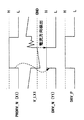
- FIG. 15 shows an operation waveform of the Nch driver 216.
- the control signal PRDRV_N output from the power supply control circuit 214 in FIG. 13 changes from “L” to “H” (the control signal PRDRV_P changes from “L” to “H” and the main transistor MP201 is turned off)
- the driver signal The drive signal DRV_N is changed from “L” to “H” by the generation unit 2162.
- the synchronous rectification transistor MN201 changes from off to on.
- a current flows from the synchronous rectification transistor MN201 to the capacitor C201 via the inductor L201. Therefore, the voltage V_LX1 of the node LX1 is a negative voltage lower than the ground voltage GND.
- the reference voltage Vref1 is set in advance so as to be the drain voltage V11 of the transistor MN202 at this time. Then, the output of the comparator 2165 is inverted from “H” to “L”, and accordingly, the drive signal DRV_N changes from “H” to “L”, and the synchronous rectification transistor MN201 is turned off. Thus, when the voltage V_LX1 of the node LX1 becomes zero, the reverse current that immediately flows from the inductor L201 toward the synchronous rectification transistor MN201 is blocked.
- Patent Document 2 discloses a stop control unit for stopping one of the pair of synchronous rectification switching elements when an output voltage exceeds a predetermined voltage in a switching power supply including the pair of synchronous rectification switching elements.
- a switching power supply comprising:
- Patent Document 3 discloses a synchronous rectification type switching regulator characterized by forcibly turning off a synchronous rectification transistor to enter a cut-off state when the occurrence of a reverse current flow is detected.
- the switching power supply device (DCDC converter) disclosed in Patent Document 1 reduces the current consumption by turning off the synchronous rectification transistor MN201 when a backflow of current occurs.
- this switching power supply device operates to turn on the rectifying transistor MN201 once and detect that the reverse current has flown even when the reverse flow of the current is likely to occur, such as when the load 213 is a low load. is required. That is, this switching power supply device needs to perform control (switch control) for turning on and off the rectifier transistor once even when the rectifier transistor MN201 should always be turned off because a reverse current tends to occur. Therefore, this switching power supply device has a problem that current consumption increases due to useless switch control of the rectifying transistor.
- the DCDC converter of the related technology has a problem that the current consumption increases due to wasteful switch control of the rectifying transistor.
- a DCDC converter is provided between a power supply control circuit that generates first and second pulse signals having a predetermined duty ratio, an input voltage terminal to which an input voltage is supplied, and an external output terminal.
- a first switch element that is controlled to be turned on / off based on a one-pulse signal; a reference voltage terminal to which a first reference voltage is supplied; and an external output terminal. The first switch element is controlled based on a second control signal.
- An inductor provided between a second switch element whose on / off is controlled to be opposite to the element, a connection point between the first and second switch elements, and the external output terminal; and the connection A comparison circuit that compares the voltage at the point with the second reference voltage and outputs a comparison result; and, based on the comparison result, the second pulse signal and a first stop signal that turns off the second switch element, what A first control circuit that outputs the first control signal as a first control signal, a detection timing at which current is determined to flow backward from the external output terminal toward the second switch element according to the comparison result, a reference timing, And a second control circuit for outputting either the first control signal or the second stop signal for turning off the second switch element as a second control signal.
- a DCDC converter control method is provided between a power supply control circuit that generates first and second pulse signals having a predetermined duty ratio, an input voltage terminal to which an input voltage is supplied, and an external output terminal.
- a first switch element that is controlled to be turned on / off based on the first pulse signal, a reference voltage terminal to which a first reference voltage is supplied, and an external output terminal, and based on a second control signal,
- An inductor provided between a second switch element whose on / off is controlled to be opposite to the first switch element, a connection point between the first and second switch elements, and the external output terminal;
- the control method of the DCDC converter comprising: a voltage at the connection point and a second reference voltage are compared and a comparison result is output, and based on the comparison result, the second pulse signal; Any one of the first stop signal for turning off the switch element is output as the first control signal, and it is determined from the comparison result that the current flows backward from the external output terminal toward the second switch element. Based on the detection timing and
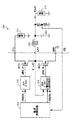
- FIG. 1 is a block diagram showing a DCDC converter 1 according to a first embodiment of the present invention.
- the DCDC converter 1 according to the present embodiment is provided on the reverse flow path when it is detected that the current is flowing backward (when it is detected that the coil current is reduced to a value close to 0).
- the reverse flow of the current is stopped by turning off the rectifying transistor. Thereby, an increase in current consumption is suppressed.
- the DCDC converter 1 according to the present embodiment is in the period of the next cycle when the timing of detecting the backflow of current in a certain cycle (backflow detection timing) is the same as or earlier than the predetermined reference timing. Continue to turn off the rectifier transistor.
- the DCDC converter according to the present embodiment can suppress unnecessary switch control of the rectifier transistor in the case of a low load in which backflow is likely to occur, and thus can further suppress an increase in current consumption. . This will be specifically described below.
- the DCDC converter 1 includes a power supply control circuit 11, a comparator (comparison circuit) 12, a flip-flop (first flip-flop, hereinafter simply referred to as DFF) 13, and a low load control circuit 14.
- AND circuit first AND circuit
- AND circuit second AND circuit, hereinafter simply referred to as AND
- MN1 rectifier transistor
- a coil (inductor) L1 a capacitor C1.
- the DFF 13 and the AND 15 constitute a first control circuit.
- the low load control circuit 14 and the AND 16 constitute a second control circuit.
- the power supply control circuit 11 is a circuit that continuously generates a pulse signal (first pulse signal) PWM_P and a pulse signal (second pulse signal) PWM_N having a predetermined duty ratio.
- the power supply control circuit 11 can appropriately change the duty ratio of the pulse signals PWM_P and PWM_N.
- the duty ratio is the ratio of the H level in one cycle of the pulse signal among the voltage levels of the H level and the L level.
- the output transistor MP1 and the rectifying transistor MN1 include an input voltage terminal (hereinafter referred to as VDD) to which a power supply voltage (input voltage) VDD is supplied, and a reference to which a reference voltage (first reference voltage) GND is supplied.
- a voltage terminal hereinafter, the terminal name is referred to as GND
- the source is connected to the input voltage terminal VDD, the drain is connected to the node LX, and the pulse signal PWM_P from the power supply control circuit 11 is applied to the gate.
- the rectifying transistor MN1 the source is connected to the reference voltage terminal GND, the drain is connected to the node LX, and a control signal S2 (described later) is applied to the gate.
- the output transistor MP1 is turned on when the pulse signal PWM_P is at L level and turned off when the pulse signal PWM_P is at H level.
- the rectifying transistor MN1 is turned on when the control signal S2 is at the H level, and is turned off when the control signal S2 is at the L level. Note that, in the normal state (a state in which no reverse current flows), the output transistor MP1 and the rectifying transistor MN1 are controlled to be turned on and off so as to conflict with each other.
- the coil L1 is provided between the node LX and the external output terminal VOUT.
- the capacitor C1 is provided between a connection point between the coil L1 and the external output terminal VOUT and the reference voltage terminal GND.
- the output transistor MP1 is turned off and the rectifier transistor MN1 is turned on, the energy accumulated in the coil L1 is released, and a current flows through the rectifier transistor MN1 toward the coil L1 to charge the capacitor C1. During this time, the current flowing through the coil L1 decreases. When a current flows toward the coil L1 via the rectifying transistor MN1, the voltage at the node LX is lower than the reference voltage GND. On the other hand, when the current flowing through the coil L1 decreases and the current starts to flow from the coil L1 via the rectifying transistor MN1, that is, when a reverse current occurs, the voltage at the node LX shows a value equal to or higher than the reference voltage GND.
- the comparator 12 the voltage of the node LX is supplied to the non-inverting input terminal, the reference voltage (second reference voltage) GND is supplied to the inverting input terminal, and the comparison result COMP_OUT is output from the output terminal. That is, the comparator 12 is a circuit that compares the voltage of the node LX with the reference voltage GND and outputs the comparison result COMP_OUT.
- the comparator 12 when the voltage of the node LX is lower than the reference voltage GND, the comparator 12 outputs an L level comparison result COMP_OUT. On the other hand, when the voltage of the node LX is equal to or higher than the reference voltage GND, the comparator 12 outputs an H level comparison result COMP_OUT.
- the comparison result COMP_OUT is input to the clock input terminal CLK
- the power supply voltage VDD H level
- the pulse signal PWM_N from the power supply control circuit 11 is input to the reset input terminal RESET_B
- the data A mask signal (first mask signal) M1 is output from the inverting output terminal Q_B.
- the DFF 13 is reset when the pulse signal PWM_N is at L level, and outputs an H level mask signal M1 from the data inversion output terminal Q_B. Further, the DFF 13 is released from the reset when the pulse signal PWM_N is at the H level.
- the comparison result COMP_OUT rises during this period, the LFF mask signal from the data inversion output terminal Q_B is synchronized with the rise of the comparison result COMP_OUT. M1 is output.
- the pulse signal PWM_N from the power supply control circuit 11 is input to one input terminal, the mask signal M1 from the DFF 13 is input to the other input terminal, and the control signal (first control signal) S1 is output from the output terminal. Is done. That is, the AND 15 is a circuit that controls whether or not the pulse signal PWM_N from the power supply control circuit 11 is directly output as the control signal S1 based on the mask signal M1.
- the AND 15 outputs the pulse signal PWM_N from the power supply control circuit 11 as it is as the control signal S1.
- the AND 15 outputs the control signal S1 (first stop signal) at L level regardless of the value of the pulse signal PWM_N.
- the low load control circuit 14 generates a mask signal (second mask signal) M2 based on a timing at which a backflow of current is detected based on the comparison result COMP_OUT (backflow detection timing) and a predetermined reference timing. Circuit. Specifically, in a certain cycle, when the pulse signal PWM_P and PWM_N are both at the H level and the switching timing of the comparison result COMP_OUT from the L level to the H level is later than the reference timing, the low load control circuit 14 Continues to output the H level mask signal M2 during the next cycle.
- the low load control circuit 14 is in the H cycle during the next cycle.
- the level mask signal M2 is continuously output.
- the low load control circuit No. 14 continues to output the L level mask signal M2 during the next cycle.
- the control signal S 1 from the AND 15 is input to one input terminal, the mask signal M 2 from the low load control circuit 14 is input to the other input terminal, and the control signal (second control signal) S 2 is output from the output terminal. Is output. That is, the AND 16 is a circuit that controls whether or not the control signal S1 from the AND 15 is directly output as the control signal S2 based on the mask signal M2.
- the AND 16 outputs the control signal S1 from the AND 15 as it is as the control signal S2.
- the AND 16 outputs the control signal S2 (second stop signal) at the L level regardless of the value of the control signal S1.
- the DCDC converter 1 shown in FIG. 1 detects the backflow of the current by the comparator 12, the backflow of the current is stopped by turning off the rectification transistor MN1. Thereby, an increase in current consumption is suppressed. Furthermore, in the DCDC converter 1 shown in FIG. 1, in a certain cycle, when the timing at which the current backflow is detected is the same as or earlier than the reference timing, that is, when the current backflow is detected at a relatively early timing, During the cycle, the rectifying transistor MN1 is kept off. Thereby, since the DCDC converter 1 shown in FIG. 1 can suppress useless switch control of the rectifying transistor MN1, it is possible to further suppress an increase in current consumption.
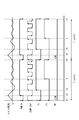
- the coil current shown in the timing charts of FIGS. 2 to 4 is a current that flows through the coil L1, and a current that flows from the node LX to the external output terminal VOUT via the coil L1 is positive.
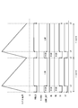
- FIG. 2 is a timing chart showing the operation of the DCDC converter 1 under a high load. Note that a high load means a state in which a large amount of current needs to be supplied to a circuit (not shown) connected to the external output terminal VOUT.
- the output transistor MP1 is turned on.
- the L-level pulse signal PWM_N is directly propagated as the control signal S2 via the ANDs 15 and 16 regardless of the values of the mask signals M1 and M2.
- the rectification transistor MN1 is turned off. Therefore, a current flows from the input voltage terminal VDD to the coil L1 via the output transistor MP1, and the capacitor C1 is charged. Thereby, the coil current flowing through the coil L1 increases, and energy is accumulated in the coil L1.
- the low load control circuit 14 does not detect a backflow of current in the previous cycle (because the coil current has not decreased to a value close to 0), so during this cycle (time t1 to t3). At times t3 to t5), the H level mask signal M2 is continuously output.
- the output transistor MP1 is turned off.
- the pulse signal PWM_N at the H level is directly propagated as the control signal S2 via the ANDs 15 and 16 because the mask signals M1 and M2 are at the H level.
- the rectification transistor MN1 is turned on. Therefore, the energy accumulated in the coil L1 is released, and a current flows toward the coil L1 through the rectifying transistor MN1 to charge the capacitor C1. During this time, the current flowing through the coil L1 decreases.
- the comparator 12 outputs an L level comparison result COMP_OUT. Therefore, the DFF 13 outputs an H level mask signal M1 at the time of reset.
- the pulse current PWM_N and PWM_P are both at the H level (time t2 to t3 and time t4 to t5), and the coil current Decreases but does not decrease to a negative value. That is, no reverse current is generated.
- the voltage of the node LX always shows a value lower than the reference voltage GND. Therefore, during this period, the comparator 12 continues to output the L level comparison result COMP_OUT. Therefore, the DFF 13 continues to output the H level mask signal M1 at the reset time during this period. Further, as described above, the low load control circuit 14 continues to output the H level mask signal M2 during this cycle. Therefore, the pulse signal PWM_N is directly propagated as the control signal S2 through the ANDs 15 and 16.
- the DCDC converter 1 In such a high load state, the current flowing through the coil L1 (coil current) repeatedly increases and decreases, but the direction does not change. That is, the DCDC converter 1 according to the present embodiment performs the same operation as a general DCDC converter when the load is high.
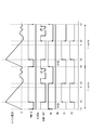
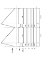
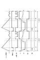
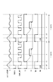
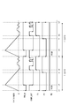
- FIG. 3 is a timing chart showing the operation of the DCDC converter 1 at the time of medium load (when the timing of reverse current flow is late).
- the medium load refers to a state in which a smaller current needs to be supplied to a circuit (not shown) connected to the external output terminal VOUT than in the case of a high load.
- the output transistor MP1 is turned on.
- the L-level pulse signal PWM_N is directly propagated as the control signal S2 via the ANDs 15 and 16 regardless of the values of the mask signals M1 and M2.
- the rectification transistor MN1 is turned off. Therefore, a current flows from the input voltage terminal VDD to the coil L1 via the output transistor MP1, and the capacitor C1 is charged. Thereby, the coil current flowing through the coil L1 increases, and energy is accumulated in the coil L1.
- the low load control circuit 14 detects a backflow of current at a timing later than a predetermined reference timing in the previous cycle (because the coil current has decreased to a value close to 0). During this cycle (time t1 to t4 and time t4 to t7), the H level mask signal M2 is continuously output.
- the output transistor MP1 is turned off.
- the pulse signal PWM_N at the H level is directly propagated as the control signal S2 via the ANDs 15 and 16 because the mask signals M1 and M2 are at the H level.
- the rectification transistor MN1 is turned on. Therefore, the energy accumulated in the coil L1 is released, and a current flows toward the coil L1 through the rectifying transistor MN1 to charge the capacitor C1. During this time, the current flowing through the coil L1 decreases.
- the comparator 12 outputs an L level comparison result COMP_OUT. Therefore, the DFF 13 outputs an H level mask signal M1 at the time of reset.
- the pulse signals PWM_N and PWM_P are both at the H level (time t2 to t4 and time t5).
- the coil current decreases to a negative value (time t3 and time t6). That is, reverse current flow occurs.
- the comparator 12 switches the comparison result COMP_OUT from the L level to the H level and outputs it.
- the DFF 13 switches the mask signal M1 from the H level to the L level and outputs it in synchronization with the rising edge of the comparison result COMP_OUT. Therefore, the control signals S1 and S2 indicate the L level regardless of the value of the pulse signal PWM_N. As a result, the rectifying transistor MN1 is turned off, and the reverse current flow is stopped.
- the low load control circuit 14 determines that the backflow detection timing (time t3 and time t6) is later than the reference timing (time X and time Y) in this cycle (time t1 to t4 and time t4 to t7). During this period, the H level mask signal M2 is continuously output.
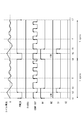
- FIG. 4 is a timing chart showing the operation of the DCDC converter 1 when the load is low (when the timing of the backflow of current is early). Note that the low load refers to a state where it is necessary to supply a smaller current than a medium load to a circuit (not shown) connected to the external output terminal VOUT.
- the output transistor MP1 is turned on.
- the L-level pulse signal PWM_N is directly propagated as the control signal S2 via the ANDs 15 and 16 regardless of the values of the mask signals M1 and M2.
- the rectification transistor MN1 is turned off. Therefore, a current flows from the input voltage terminal VDD to the coil L1 via the output transistor MP1, and the capacitor C1 is charged. Thereby, the coil current flowing through the coil L1 increases, and energy is accumulated in the coil L1.
- the low load control circuit 14 detects the backflow of current at the same timing or earlier than the reference timing determined in advance in the previous cycle (the coil current decreases to a value close to 0). Therefore, during this cycle (time t1 to t4 and time t4 to t7), the L level mask signal M2 is continuously output.
- the output transistor MP1 is turned off.
- the control signal S2 becomes the L level. Therefore, the rectifying transistor MN1 is turned off regardless of the value of the pulse signal PWM_N. Therefore, no reverse current occurs.
- the case where a parasitic diode is formed in the rectifying transistor MN1 is also considered. That is, the energy accumulated in the coil L1 is released, a current flows through the parasitic diode of the rectifying transistor MN1 toward the coil L1, and the capacitor C1 is charged. During this time, the current flowing through the coil L1 decreases.
- the comparator 12 outputs an L level comparison result COMP_OUT. Therefore, the DFF 13 outputs an H level mask signal M1 at the time of reset.
- the pulse signals PWM_N and PWM_P are both at the H level (time t2 to t4 and time). From t5 to t7), the coil current decreases to a value near 0 at a timing earlier than the reference timing (time X and time Y) (time t3 and time t6). In other words, at time t3 and time t6, the voltage of the node LX shows a value equal to or higher than the reference voltage GND. At this time, the comparator 12 switches the comparison result COMP_OUT from the L level to the H level and outputs it.
- the DFF 13 switches the mask signal M1 from the H level to the L level and outputs it in synchronization with the rising edge of the comparison result COMP_OUT.
- the low load control circuit 14 continues to output the L level mask signal M2 during this cycle as described above. Therefore, the control signal S2 indicates the L level during the cycle, regardless of the value of the pulse signal PWM_N.
- the low load control circuit 14 has the same or earlier backflow detection timing (time t3 and time t6) than the reference timing (time X and time Y) in this cycle (time t1 to t4 and time t4 to t7).
- the L level mask signal M2 is continuously output.
- the DCDC converter 1 continues to turn off the rectifying transistor MN1 during the next cycle, thereby stopping the reverse current flow and suppressing unnecessary switch control. As a result, an increase in current consumption is further suppressed at the time of a low load where current backflow is likely to occur.
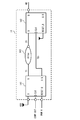
- FIG. 5 is a diagram showing a specific circuit configuration of the low load control circuit 14. As illustrated in FIG. 5, the low load control circuit 14 includes a DFF (second flip-flop) 141, a DFF (third flip-flop) 142, and a delay circuit 143.
- DFF second flip-flop
- DFF third flip-flop
- the comparison result COMP_OUT is input to the clock input terminal CLK
- the power supply voltage VDD H level
- the pulse signal PWM_N from the power supply control circuit 11 is input to the reset input terminal RESET_B
- the data An intermediate signal T1 is output from the output terminal Q
- an intermediate inversion signal TB1 is output from the data inversion output terminal Q_B.
- the delay circuit 143 the intermediate signal T1 is input to the input terminal, and the delay signal D1 is output from the output terminal.
- the intermediate inverted signal TB1 from the DFF 141 is input to the clock input terminal CLK
- the delay signal D1 from the delay circuit 143 is input to the data input terminal D
- the power supply voltage VDD (H level) is input to the reset input terminal RESET_B. Then, the mask signal M2 is output from the data output terminal Q.
- the DFF 141 is reset when the pulse signal PWM_N is at the L level, outputs the L level intermediate signal T1 from the data output terminal Q, and outputs the H level intermediate inverted signal TB1 from the data inversion output terminal Q_B. Further, the DFF 141 is released from the reset when the pulse signal PWM_N is at the H level. When the comparison result COMP_OUT rises during this period, the DFF 141 is synchronized with the rise of the comparison result COMP_OUT from the data output terminal Q to the H level intermediate signal. In addition to outputting T1, an intermediate inverted signal TB1 of L level is output from the data inverted output terminal Q_B.
- the delay circuit 143 adds a predetermined delay to the intermediate signal T1, inverts it, and outputs it as a delay signal D1.
- the DFF 142 takes in the delay signal D1 in synchronization with the rising edge of the intermediate inverted signal TB1 and outputs it as a mask signal M2.
- FIG. 6 is a timing chart showing the operation of the low load control circuit 14 at high load.
- the timing chart shown in FIG. 6 shows the operation of the low load control circuit 14 when the DCDC converter 1 is operated under the same conditions as in FIG.
- the comparator 12 when the pulse signals PWM_N and PWM_P are at the L level, the comparator 12 outputs the comparison result COMP_OUT at the H level (time t1 to t2 and time t3 to t4). However, since the DFF 141 is reset by the L level pulse signal PWM_N, the DFF 141 outputs the L level intermediate signal T1 and outputs the H level intermediate inversion signal TB1.
- the DFF 142 continues to output the H level mask signal M2 at the time of reset. Details will be described later.
- the comparator 12 outputs an L level comparison result COMP_OUT.
- the pulse current PWM_N and PWM_P are both at the H level (time t2 to t3 and time t4 to t5), and the coil current Decreases but does not decrease to a negative value. That is, no reverse current is generated.
- the comparator 12 continues to output the L level comparison result COMP_OUT.
- the DFF 141 continues to output the L-level intermediate signal T1 and the H-level intermediate inverted signal TB1 at the time of reset.
- the delay circuit 143 outputs an H level delay signal D1. Therefore, the DFF 142 continues to output the H level mask signal M2 at the reset time during the next cycle.
- the low load control circuit 14 continues to output the mask signal M2 at the H level during the period of the next cycle when no reverse current flows in a certain cycle.
- FIG. 7 is a timing chart showing the operation of the low load control circuit 14 at a medium load.
- the timing chart shown in FIG. 7 shows the operation of the low load control circuit 14 when the DCDC converter 1 is operated under the same conditions as in FIG.
- the comparator 12 when the pulse signals PWM_N and PWM_P are at the L level, the comparator 12 outputs the comparison result COMP_OUT at the H level (time t1 to t2 and time t4 to t5). However, since the DFF 141 is reset by the L level pulse signal PWM_N, the DFF 141 outputs the L level intermediate signal T1 and outputs the H level intermediate inversion signal TB1.
- the DFF 142 continues to output the H level mask signal M2. Details will be described later.
- the comparator 12 outputs an L level comparison result COMP_OUT.
- the pulse signals PWM_N and PWM_P are both at the H level (time t2 to t4 and time t5).
- the coil current decreases to a negative value (time t3 and time t6). That is, reverse current flow occurs.
- the comparator 12 switches the comparison result COMP_OUT from the L level to the H level and outputs it.
- the DFF 141 switches and outputs the intermediate signal T1 from the L level to the H level and outputs the intermediate inverted signal TB1 from the H level to the L level in synchronization with the rising of the comparison result COMP_OUT.
- the delay circuit 143 adds a predetermined delay to the intermediate signal T1, inverts it, and outputs it as a delay signal D1.
- the delay circuit 142 adds a delay having a length corresponding to the period X to t4 to the intermediate signal T1, inverts it, and outputs it as a delay signal D1.
- the DFF 142 When the intermediate inverted signal TB1 is reset to the H level by switching the pulse signal PWM_N from the H level to the L level (time t4 and time t7), the DFF 142 is synchronized with the rising edge of the intermediate inverted signal TB1. Capture.
- the backflow detection timing time t3 and time t6
- the reference timing time X and time Y
- the DFF 142 takes in the delay signal D1 in the H level state and outputs it as the mask signal M2. That is, the DFF 142 continues to output the H level mask signal M2 during the next cycle.
- the low load control circuit 14 continues to output the H level mask signal M2 during the next cycle.
- FIG. 8 is a timing chart showing the operation of the low load control circuit 14 at low load.
- the timing chart shown in FIG. 8 shows the operation of the low load control circuit 14 when the DCDC converter 1 is operated under the same conditions as in FIG.
- the comparator 12 when the pulse signals PWM_N and PWM_P are at the L level, the comparator 12 outputs the comparison result COMP_OUT at the H level (time t1 to t2 and time t4 to t5). However, since the DFF 141 is reset by the L level pulse signal PWM_N, the DFF 141 outputs the L level intermediate signal T1 and outputs the H level intermediate inversion signal TB1.
- the DFF 142 continues to output the L level mask signal M2. Details will be described later.
- the comparator 12 outputs an L level comparison result COMP_OUT.
- the pulse signals PWM_N and PWM_P are both at the H level (time t2 to t4 and time t4). From t5 to t7), the coil current decreases to a value near 0 at a timing earlier than the reference timing (time X and time Y) (time t3 and time t6). In other words, at time t3 and time t6, the voltage of the node LX shows a value equal to or higher than the reference voltage GND.
- the comparator 12 switches the comparison result COMP_OUT from the L level to the H level and outputs it.
- the DFF 141 switches and outputs the intermediate signal T1 from the L level to the H level and outputs the intermediate inverted signal TB1 from the H level to the L level in synchronization with the rising of the comparison result COMP_OUT.
- the delay circuit 143 adds a predetermined delay to the intermediate signal T1, inverts it, and outputs it as a delay signal D1.
- the delay circuit 142 adds a delay having a length corresponding to the period X to t4 to the intermediate signal T1, inverts it, and outputs it as a delay signal D1.
- the DFF 142 When the intermediate inverted signal TB1 is reset to the H level by switching the pulse signal PWM_N from the H level to the L level (time t4 and time t7), the DFF 142 is synchronized with the rising edge of the intermediate inverted signal TB1. Capture.
- the backflow detection timing time t3 and time t6
- the reference timing time X and time Y
- the DFF 142 takes in the delay signal D1 in the L level state and outputs it as the mask signal M2. That is, the DFF 142 continues to output the L level mask signal M2 during the next cycle.
- the low load control circuit 14 continues to output the L level mask signal M2 during the next cycle.
- the DCDC converter 1 according to the present embodiment detects a reverse current flow (when it detects that the coil current has decreased to a value close to 0), By turning it off, the reverse current flow is stopped. Thereby, an increase in current consumption is suppressed. Furthermore, the DCDC converter 1 according to the present embodiment continues to turn off the rectifier transistor during the next cycle when the backflow detection timing is the same as or earlier than the reference timing in a certain cycle. As a result, the DCDC converter 1 according to the present embodiment can suppress unnecessary switch control of the rectifier transistor in the case of a low load in which backflow is likely to occur, and thus can further suppress an increase in current consumption.
- the DCDC converter 1 can suppress wasteful switch control by turning off the rectifier transistor in advance in the case of a low load where current backflow is likely to occur. Can be suppressed.
- the delay added to the intermediate signal T1 by the delay circuit 143 can be adjusted.
- the low load control circuit 14 can be realized by a simple circuit configuration including two DFFs 141 and 142 and a delay circuit 143. In the present embodiment, the case where the low load control circuit 14 is applied to the step-down circuit has been described as an example, but the present invention is not limited to this.
- the low load control circuit 14 can be applied not only to the step-down circuit but also to the step-up circuit, the step-up / step-down circuit, and the polarity inversion circuit.
- Embodiment 2 In the present embodiment, another configuration example of the low load control circuit 14 will be described as a low load control circuit 14a.
- FIG. 9 shows a specific circuit configuration of the low load control circuit 14a. As illustrated in FIG. 9, the low load control circuit 14 a includes a DFF 141, a DFF 142, and a pulse generation circuit 144.
- the comparison result COMP_OUT is input to the clock input terminal CLK
- the power supply voltage VDD H level
- the pulse signal PWM_N from the power supply control circuit 11 is input to the reset input terminal RESET_B
- the data An intermediate signal T1 is output from the output terminal Q.
- a determination signal is input to the input terminal, and a pulse signal (third pulse signal) P1 is output from the output terminal.
- the pulse signal P1 from the pulse generation circuit 144 is input to the clock input terminal CLK
- the intermediate signal T1 from the DFF 141 is input to the data input terminal D
- the power supply voltage VDD (H level) is input to the reset input terminal RESET_B.
- the mask signal M2 is output from the data inversion output terminal Q_B.
- the DFF 141 is reset when the pulse signal PWM_N is at L level, and outputs an intermediate signal T1 at L level from the data output terminal Q. Further, the DFF 141 is released from the reset when the pulse signal PWM_N is at the H level. When the comparison result COMP_OUT rises during this period, the DFF 141 is synchronized with the rise of the comparison result COMP_OUT from the data output terminal Q to the H level intermediate signal. Output T1.
- the pulse generation circuit 144 outputs a pulse signal P1 having a predetermined period based on the determination signal output from the power supply control circuit 11.
- a case where the pulse signal P1 has the same cycle as the pulse signal PWM_N and the duty ratio is different will be described as an example.
- the DFF 142 takes in the intermediate signal T1 in synchronization with the rising edge of the pulse signal P1, and outputs the inverted signal as the mask signal M2.
- FIG. 10 is a timing chart showing the operation of the low load control circuit 14a at the time of high load.
- the timing chart shown in FIG. 10 shows the operation of the low load control circuit 14a when the DCDC converter 1 is operated under the same conditions as in FIG.
- the comparator 12 when the pulse signals PWM_N and PWM_P are at the L level, the comparator 12 outputs the H level comparison result COMP_OUT (time t1 to t2 and time t3 to t4). However, since the DFF 141 is reset by the L level pulse signal PWM_N, it outputs the L level intermediate signal T1.
- the comparator 12 outputs an L level comparison result COMP_OUT.
- the pulse current PWM_N and PWM_P are both at the H level (time t2 to t3 and time t4 to t5), and the coil current Decreases but does not decrease to a negative value. That is, no reverse current is generated.
- the voltage of the node LX always shows a value lower than the reference voltage GND. Therefore, during this period, the comparator 12 continues to output the L level comparison result COMP_OUT. Therefore, during this period, the DFF 141 continues to output the L-level intermediate signal T1 at the time of reset.
- the pulse generation circuit 144 falls in synchronization with the fall of the pulse signal PWM_N (time t1 and time t3) based on the determination signal from the power supply control circuit 11, and after a predetermined period has elapsed from the rise of the pulse signal PWM_N. It rises at the reference timing (time X and time Y).
- the DFF 142 takes in the L-level intermediate signal T1 in synchronization with the rising edge of the pulse signal P1, and continues to output the H-level mask signal M2, which is an inverted signal, until the next rising edge of the pulse signal P1.
- the low load control circuit 14a continues to output the H level mask signal M2 when no backflow of current occurs.
- FIG. 11 is a timing chart showing the operation of the low load control circuit 14a during a medium load.
- the timing chart shown in FIG. 11 shows the operation of the low load control circuit 14a when the DCDC converter 1 is operated under the same conditions as in FIG.
- the comparator 12 when the pulse signals PWM_N and PWM_P are at the L level, the comparator 12 outputs the comparison result COMP_OUT at the H level (time t1 to t2 and time t4 to t5). However, since the DFF 141 is reset by the L level pulse signal PWM_N, it outputs the L level intermediate signal T1.
- the comparator 12 outputs an L level comparison result COMP_OUT.
- the energy accumulated in the coil L1 is smaller than that in the case of a high load.
- the coil current decreases to a negative value (time t3 and time t6). That is, reverse current flow occurs.
- the comparator 12 switches the comparison result COMP_OUT from the L level to the H level and outputs it.
- the DFF 141 switches the intermediate signal T1 from the L level to the H level and outputs it in synchronization with the rise of the comparison result COMP_OUT.
- the pulse generation circuit 144 falls in synchronization with the fall of the pulse signal PWM_N based on the determination signal from the power supply control circuit 11 (time t1 and time t3), and after a predetermined period has elapsed from the rise of the pulse signal PWM_N. It rises at the reference timing (time X and time Y).
- the backflow detection timing (time t3 and time t6) is later than the reference timing (time X and time Y). Therefore, the DFF 142 takes in the L-level intermediate signal T1 in synchronization with the rising edge of the pulse signal P1, and continues to output the H-level mask signal M2 that is an inverted signal until the next rising edge of the pulse signal P1.
- the low load control circuit 14a continues to output the H level mask signal M2 from the reference timing to the reference timing of the next cycle.
- FIG. 12 is a timing chart showing the operation of the low load control circuit 14a when the load is low.
- the timing chart shown in FIG. 12 shows the operation of the low load control circuit 14a when the DCDC converter 1 is operated under the same conditions as in FIG.
- the comparator 12 when the pulse signals PWM_N and PWM_P are at L level, the comparator 12 outputs a comparison result COMP_OUT at H level (time t1 to t2 and time t4 to t5). However, since the DFF 141 is reset by the L level pulse signal PWM_N, it outputs the L level intermediate signal T1.
- the comparator 12 outputs an L level comparison result COMP_OUT.
- the energy accumulated in the coil L1 is further smaller than in the case of the medium load, so that the pulse signals PWM_N and PWM_P are both at the H level (time t2 to t4 and time).
- the coil current decreases to a value near 0 at a timing earlier than the reference timing (time X and time Y) (time t3 and time t6).
- the voltage of the node LX shows a value equal to or higher than the reference voltage GND.
- the comparator 12 switches the comparison result COMP_OUT from the L level to the H level and outputs it.
- the DFF 141 switches the intermediate signal T1 from the L level to the H level and outputs it in synchronization with the rise of the comparison result COMP_OUT.
- the pulse generation circuit 144 falls in synchronization with the fall of the pulse signal PWM_N (time t1 and time t3) based on the determination signal from the power supply control circuit 11, and after a predetermined period has elapsed from the rise of the pulse signal PWM_N. It rises at the reference timing (time X and time Y).
- the backflow detection timing (time t3 and time t6) is earlier than the reference timing (time X and time Y). Accordingly, the DFF 142 takes in the H-level intermediate signal T1 in synchronization with the rising edge of the pulse signal P1, and continues to output the L-level mask signal M2, which is an inverted signal, until the next rising edge of the pulse signal P1.
- the low load control circuit 14a continues to output the L level mask signal M2 from the reference timing to the reference timing of the next cycle.
- the DCDC converter 1 according to the first and second embodiments is provided on the reverse flow path when detecting the reverse flow of the current (detecting that the coil current has decreased to a value close to 0).
- the reverse flow of the current is stopped by turning off the rectifying transistor.
- the DCDC converter 1 according to the first and second embodiments keeps the rectifying transistor off during the next cycle when the backflow detection timing is the same as or earlier than the reference timing in a certain cycle.
- the DCDC converter according to the present embodiment can suppress unnecessary switch control of the rectifier transistor in the case of a low load in which backflow is likely to occur, and can further suppress an increase in current consumption.
- the present invention is not limited to the above-described embodiment, and can be appropriately changed without departing from the spirit of the present invention.
- the case where the comparator 12 compares the voltage of the node LX with the reference voltage GND has been described as an example.
- the comparator 12 can be appropriately changed to a circuit configuration that compares the voltage of the node LX with a second reference voltage having a voltage level different from the reference voltage GND. In this case, even when the current does not necessarily flow backward, the comparator 12 determines that the current is “current is flowing backward” and outputs the comparison result.
- the rectification transistor MN1 is always controlled to be off at the time of a low load
- the present invention is not limited to this.
- the mask signal M2 indicates the L level and the rectification transistor MN1 is kept off, so that it may be determined that no reverse current has occurred.
- the mask signal M2 indicates the H level during the next cycle. Such an operation is repeated, and there is a possibility that the voltage level of the mask signal M2 is alternately switched every cycle.
- the determination signal is output from the power supply control circuit 11 as an example, but the present invention is not limited to this. It is possible to appropriately change to a circuit configuration in which the determination signal is supplied from the outside.
Landscapes
- Engineering & Computer Science (AREA)
- Power Engineering (AREA)
- Dc-Dc Converters (AREA)
Abstract
Description
図1は、本発明の実施の形態1にかかるDCDCコンバータ1を示すブロック図である。本実施の形態にかかるDCDCコンバータ1は、電流が逆流していることを検出した場合(コイル電流が0付近の値まで減少していることを検出した場合)に、逆流経路上に設けられた整流トランジスタをオフにすることにより電流の逆流を停止させる。それにより、消費電流の増大が抑制される。さらに、本実施の形態にかかるDCDCコンバータ1は、あるサイクルにおいて電流の逆流を検出したタイミング(逆流検出タイミング)が予め決められた基準タイミングと同じ又はそれより早い場合に、次のサイクルの期間中、整流トランジスタをオフにし続ける。それにより、本実施の形態にかかるDCDCコンバータは、逆流の発生しやすい低負荷の場合に、整流トランジスタの無駄なスイッチ制御を抑制することができるため、さらに消費電流の増大を抑制することができる。以下、具体的に説明する。
次に、図1に示すDCDCコンバータ1の動作を、図2~図4のタイミングチャートを用いて説明する。なお、図2~図4のタイミングチャート中に示すコイル電流とは、コイルL1に流れる電流であって、ノードLXからコイルL1を介して外部出力端子VOUTに向けて流れる電流を正としている。
図5は、低負荷制御回路14の具体的な回路構成を示す図である。図5に示すように、低負荷制御回路14は、DFF(第2フリップフロップ)141と、DFF(第3フリップフロップ)142と、遅延回路143と、を有する。
次に、図5に示す低負荷制御回路14の動作を、図6~図8のタイミングチャートを用いて説明する。
本実施の形態では、低負荷制御回路14の他の構成例を低負荷制御回路14aとして説明する。図9は、低負荷制御回路14aの具体的な回路構成を示すである。図9に示すように、低負荷制御回路14aは、DFF141と、DFF142と、パルス生成回路144と、を有する。
次に、図9に示す低負荷制御回路14aの動作を、図10~図12のタイミングチャートを用いて説明する。
12 コンパレータ
13 フリップフロップ
14 低負荷制御回路
14a 低負荷制御回路
141 フリップフロップ
142 遅延回路
143 フリップフロップ
144 パルス生成回路
15 論理積回路
16 論理積回路
MP1 出力トランジスタ
MN1 整流トランジスタ
L1 コイル
C1 キャパシタ
Claims (16)
- 所定のデューティ比の第1及び第2パルス信号を生成する電源制御回路と、
入力電圧の供給される入力電圧端子と外部出力端子との間に設けられ、前記第1パルス信号に基づいてオンオフが制御される第1スイッチ素子と、
第1基準電圧の供給される基準電圧端子と前記外部出力端子との間に設けられ、第2制御信号に基づいてオンオフが制御される第2スイッチ素子と、
前記第1及び第2スイッチ素子との間の接続点と、前記外部出力端子と、の間に設けられたインダクタと、
前記接続点の電圧と第2基準電圧とを比較して比較結果を出力する比較回路と、
前記比較結果に基づき、前記第2スイッチ素子を前記第1スイッチ素子と相補的にオンオフする前記第2パルス信号と、前記第2スイッチ素子をオフする第1停止信号と、の何れかを第1制御信号として出力する第1制御回路と、
前記比較結果により前記外部出力端子から前記第2スイッチ素子に向けて電流が逆流していると判定された検出タイミングと、基準タイミングと、に基づき、前記第1制御信号と、前記第2スイッチ素子をオフする第2停止信号と、の何れかを前記第2制御信号として出力する第2制御回路と、を備えたDCDCコンバータ。 - 前記外部出力端子と前記インダクタとの間の接続点と基準電圧端子との間にキャパシタをさらに備えた請求項1に記載のDCDCコンバータ。
- 前記第1制御回路は、
前記比較結果により前記外部出力端子から前記第2スイッチ素子に向けて電流が逆流していると判定された場合、前記第1停止信号を前記第1制御信号として出力することを特徴とする請求項1又は2に記載のDCDCコンバータ。 - 前記第1制御回路は、
前記比較結果により前記第2スイッチ素子から前記外部出力端子に向けて電流が流れていると判定されている場合、前記第2パルス信号を前記第1制御信号として出力することを特徴とする請求項1~3の何れか一項に記載のDCDCコンバータ。 - 前記第1制御回路は、
前記比較結果及び前記第2パルス信号に基づいて第1マスク信号を生成する第1フリップフロップと、
前記第2パルス信号及び前記第1マスク信号の論理積を前記第1制御信号として出力する第1論理積回路と、を備えた請求項1~4のいずれか一項に記載のDCDCコンバータ。 - 前記第1フリップフロップは、
前記比較結果の論理値が電流の逆流を示す論理値に変化したことに応じて所定論理値の前記第1マスク信号を生成するとともに、前記第2パルス信号の論理値が前記第2スイッチ素子をオフする論理値に変化したことに応じて前記第1マスク信号を初期化することを特徴とする請求項5に記載のDCDCコンバータ。 - 前記第2制御回路は、
前記検出タイミングが前記基準タイミングより遅い場合、前記第1制御信号を前記第2制御信号として出力することを特徴とする請求項1~6のいずれか一項に記載のDCDCコンバータ。 - 前記第2制御回路は、
前記検出タイミングが前記基準タイミングと同じ又はそれより早い場合、前記第2停止信号を前記第2制御信号として出力することを特徴とする請求項1~7の何れか一項に記載のDCDCコンバータ。 - 前記第2制御回路は、
前記比較結果により前記第2スイッチ素子から前記外部出力端子に向けて電流が流れていると判定されている場合、前記第1制御信号を前記第2制御信号として出力することを特徴とする請求項1~8のいずれか一項に記載のDCDCコンバータ。 - 前記第2制御回路は、
前記検出タイミングと前記基準タイミングとに基づき第2マスク信号を生成する低負荷制御回路と、
前記第1制御信号及び前記第2マスク信号の論理積を前記第2制御信号として出力する第2論理積回路と、を備えた請求項1~9のいずれか一項に記載のDCDCコンバータ。 - 前記低負荷制御回路は、
前記比較結果の論理値が電流の逆流を示す論理値に変化したことに応じて所定論理値の中間信号を生成するとともに、前記第2パルス信号の論理値が前記第2スイッチ素子をオフする論理値に変化したことに応じて前記中間信号を初期化する第2フリップフロップと、
前記中間信号に所定の遅延が付加された遅延信号を前記中間信号に同期して取り込み、前記第2マスク信号として出力する第3フリップフロップと、を有する請求項10に記載のDCDCコンバータ。 - 前記低負荷制御回路は、
前記比較結果の論理値が電流の逆流を示す論理値に変化したことに応じて所定論理値の中間信号を生成するとともに、前記第2パルス信号の論理値が前記第2スイッチ素子をオフする論理値に変化したことに応じて前記中間信号を初期化する第2フリップフロップと、
前記第2パルス信号に応じた周期の第3パルス信号を生成するパルス生成回路と、
前記第3パルス信号に同期して前記中間信号を取り込み、前記第2マスク信号として出力する第3フリップフロップと、を有する請求項10に記載のDCDCコンバータ。 - 前記基準タイミングは、前記第2パルス信号の論理値変化のタイミングに基づいて決定されることを特徴とする請求項1~12のいずれか一項に記載のDCDCコンバータ。
- 前記第1基準電圧と前記第2基準電圧とは同一の電圧レベルであることを特徴とする請求項1~13のいずれか一項に記載のDCDCコンバータ。
- 前記第1基準電圧と前記第2基準電圧とは異なる電圧レベルであることを特徴とする請求項1~13のいずれか一項に記載のDCDCコンバータ。
- 所定のデューティ比の第1及び第2パルス信号を生成する電源制御回路と、
入力電圧の供給される入力電圧端子と外部出力端子との間に設けられ、前記第1パルス信号に基づいてオンオフが制御される第1スイッチ素子と、
第1基準電圧の供給される基準電圧端子と前記外部出力端子との間に設けられ、第2制御信号に基づいてオンオフが制御される第2スイッチ素子と、
前記第1及び第2スイッチ素子との間の接続点と、前記外部出力端子と、の間に設けられたインダクタと、を備えたDCDCコンバータの制御方法であって、
前記接続点の電圧と第2基準電圧とを比較して比較結果を出力し、
前記比較結果に基づき、前記第2スイッチ素子を前記第1スイッチ素子と相補的にオンオフする前記第2パルス信号と、前記第2スイッチ素子をオフする第1停止信号と、の何れかを第1制御信号として出力し、
前記比較結果により前記外部出力端子から前記第2スイッチ素子に向けて電流が逆流していると判定された検出タイミングと、基準タイミングと、に基づき、前記第1制御信号と、前記第2スイッチ素子をオフする第2停止信号と、の何れかを前記第2制御信号として出力するDCDCコンバータの制御方法。
Priority Applications (3)
| Application Number | Priority Date | Filing Date | Title |
|---|---|---|---|
| US14/112,813 US9209695B2 (en) | 2011-04-20 | 2012-04-11 | DC-DC converter and control method for the same |
| JP2013510865A JP5651234B2 (ja) | 2011-04-20 | 2012-04-11 | Dcdcコンバータ及びその制御方法 |
| US14/934,723 US20160065074A1 (en) | 2011-04-20 | 2015-11-06 | Dc-dc converter and control method for the same |
Applications Claiming Priority (2)
| Application Number | Priority Date | Filing Date | Title |
|---|---|---|---|
| JP2011094305 | 2011-04-20 | ||
| JP2011-094305 | 2011-04-20 |
Related Child Applications (2)
| Application Number | Title | Priority Date | Filing Date |
|---|---|---|---|
| US14/112,813 A-371-Of-International US9209695B2 (en) | 2011-04-20 | 2012-04-11 | DC-DC converter and control method for the same |
| US14/934,723 Continuation US20160065074A1 (en) | 2011-04-20 | 2015-11-06 | Dc-dc converter and control method for the same |
Publications (1)
| Publication Number | Publication Date |
|---|---|
| WO2012144163A1 true WO2012144163A1 (ja) | 2012-10-26 |
Family
ID=47041297
Family Applications (1)
| Application Number | Title | Priority Date | Filing Date |
|---|---|---|---|
| PCT/JP2012/002519 Ceased WO2012144163A1 (ja) | 2011-04-20 | 2012-04-11 | Dcdcコンバータ及びその制御方法 |
Country Status (3)
| Country | Link |
|---|---|
| US (2) | US9209695B2 (ja) |
| JP (1) | JP5651234B2 (ja) |
| WO (1) | WO2012144163A1 (ja) |
Cited By (3)
| Publication number | Priority date | Publication date | Assignee | Title |
|---|---|---|---|---|
| JP2015070679A (ja) * | 2013-09-27 | 2015-04-13 | ルネサスエレクトロニクス株式会社 | 半導体装置及びその制御方法 |
| CN110311562A (zh) * | 2019-07-26 | 2019-10-08 | 佛山中科芯蔚科技有限公司 | 一种直流-直流变换器 |
| WO2023242911A1 (ja) * | 2022-06-13 | 2023-12-21 | 日清紡マイクロデバイス株式会社 | Dc/dcコンバータ |
Families Citing this family (4)
| Publication number | Priority date | Publication date | Assignee | Title |
|---|---|---|---|---|
| TWI483519B (zh) * | 2013-03-29 | 2015-05-01 | Richtek Technology Corp | 動態調整電源轉換電路中的功率開關截止時間的控制電路 |
| TWI551029B (zh) * | 2015-03-13 | 2016-09-21 | 晶致半導體股份有限公司 | 具有馬達停轉設定之馬達驅動裝置及其驅動方法 |
| US11011975B2 (en) * | 2018-02-20 | 2021-05-18 | Texas Instruments Incorporated | Boost power factor correction conversion |
| KR20230144897A (ko) * | 2022-04-08 | 2023-10-17 | 삼성전자주식회사 | 펄스 스킵 기능과 온-타임 제어 기능을 포함하는 dc-dc 컨버터, 및 이를 포함하는 전자 장치들 |
Citations (5)
| Publication number | Priority date | Publication date | Assignee | Title |
|---|---|---|---|---|
| JP2000092824A (ja) * | 1998-09-10 | 2000-03-31 | Matsushita Electric Ind Co Ltd | スイッチングレギュレータおよびlsiシステム |
| JP2006158097A (ja) * | 2004-11-30 | 2006-06-15 | Renesas Technology Corp | 電源制御用半導体集積回路および電子部品並びに電源装置 |
| JP2007318909A (ja) * | 2006-05-25 | 2007-12-06 | Nec Computertechno Ltd | スイッチング電源及びその電源制御部 |
| JP2009071920A (ja) * | 2007-09-11 | 2009-04-02 | Ricoh Co Ltd | 同期整流型スイッチングレギュレータ |
| JP2010239778A (ja) * | 2009-03-31 | 2010-10-21 | New Japan Radio Co Ltd | スイッチング電源装置 |
Family Cites Families (9)
| Publication number | Priority date | Publication date | Assignee | Title |
|---|---|---|---|---|
| JP4751105B2 (ja) * | 2005-05-26 | 2011-08-17 | ローム株式会社 | 電源装置の制御回路、それを用いた電源装置ならびに電子機器 |
| JP4997891B2 (ja) * | 2006-09-15 | 2012-08-08 | 富士通セミコンダクター株式会社 | Dc−dcコンバータ及びdc−dcコンバータの制御方法 |
| TWI330775B (en) * | 2007-01-23 | 2010-09-21 | Richtek Technology Corp | Quick response switching regulator and control method thereof |
| US7782035B2 (en) * | 2007-03-28 | 2010-08-24 | Intersil Americas Inc. | Controller and driver communication for switching regulators |
| JP4720821B2 (ja) * | 2007-12-14 | 2011-07-13 | ミツミ電機株式会社 | Dc−dcコンバータおよび電源制御用半導体集積回路 |
| JP5458686B2 (ja) * | 2009-06-16 | 2014-04-02 | 日本テキサス・インスツルメンツ株式会社 | 降圧型コンバータ |
| GB0912745D0 (en) * | 2009-07-22 | 2009-08-26 | Wolfson Microelectronics Plc | Improvements relating to DC-DC converters |
| JP5730520B2 (ja) * | 2010-09-03 | 2015-06-10 | スパンション エルエルシー | スイッチングレギュレータ |
| JP5806481B2 (ja) * | 2011-02-23 | 2015-11-10 | スパンション エルエルシー | 制御回路、電子機器及び電源の制御方法 |
-
2012
- 2012-04-11 JP JP2013510865A patent/JP5651234B2/ja active Active
- 2012-04-11 US US14/112,813 patent/US9209695B2/en active Active
- 2012-04-11 WO PCT/JP2012/002519 patent/WO2012144163A1/ja not_active Ceased
-
2015
- 2015-11-06 US US14/934,723 patent/US20160065074A1/en not_active Abandoned
Patent Citations (5)
| Publication number | Priority date | Publication date | Assignee | Title |
|---|---|---|---|---|
| JP2000092824A (ja) * | 1998-09-10 | 2000-03-31 | Matsushita Electric Ind Co Ltd | スイッチングレギュレータおよびlsiシステム |
| JP2006158097A (ja) * | 2004-11-30 | 2006-06-15 | Renesas Technology Corp | 電源制御用半導体集積回路および電子部品並びに電源装置 |
| JP2007318909A (ja) * | 2006-05-25 | 2007-12-06 | Nec Computertechno Ltd | スイッチング電源及びその電源制御部 |
| JP2009071920A (ja) * | 2007-09-11 | 2009-04-02 | Ricoh Co Ltd | 同期整流型スイッチングレギュレータ |
| JP2010239778A (ja) * | 2009-03-31 | 2010-10-21 | New Japan Radio Co Ltd | スイッチング電源装置 |
Cited By (3)
| Publication number | Priority date | Publication date | Assignee | Title |
|---|---|---|---|---|
| JP2015070679A (ja) * | 2013-09-27 | 2015-04-13 | ルネサスエレクトロニクス株式会社 | 半導体装置及びその制御方法 |
| CN110311562A (zh) * | 2019-07-26 | 2019-10-08 | 佛山中科芯蔚科技有限公司 | 一种直流-直流变换器 |
| WO2023242911A1 (ja) * | 2022-06-13 | 2023-12-21 | 日清紡マイクロデバイス株式会社 | Dc/dcコンバータ |
Also Published As
| Publication number | Publication date |
|---|---|
| US20160065074A1 (en) | 2016-03-03 |
| US9209695B2 (en) | 2015-12-08 |
| JPWO2012144163A1 (ja) | 2014-07-28 |
| JP5651234B2 (ja) | 2015-01-07 |
| US20140043005A1 (en) | 2014-02-13 |
Similar Documents
| Publication | Publication Date | Title |
|---|---|---|
| JP5451123B2 (ja) | 電源装置,電源制御装置及び電源装置の制御方法 | |
| JP5651234B2 (ja) | Dcdcコンバータ及びその制御方法 | |
| KR100912865B1 (ko) | 스위칭 레귤레이터 및 그 스위칭 레귤레이터를 구비하는반도체 장치 | |
| JP5211959B2 (ja) | Dc−dcコンバータ | |
| JP5262260B2 (ja) | 電圧可変dc−dcコンバータ | |
| JP4710749B2 (ja) | Dc−dcコンバータの制御回路及び方法 | |
| JP4899624B2 (ja) | Dc−dcコンバータ及びdc−dcコンバータの制御回路 | |
| JP5304281B2 (ja) | Dc−dcコンバータおよびスイッチング制御回路 | |
| JP4045292B1 (ja) | 同期整流型スイッチングレギュレータ、同期整流型スイッチングレギュレータの制御回路及び同期整流型スイッチングレギュレータの動作制御方法 | |
| JP2014050308A (ja) | スイッチングレギュレータとその制御方法 | |
| JP5865028B2 (ja) | Dcーdcコンバータ | |
| WO2006137213A1 (ja) | 降圧型スイッチングレギュレータ、その制御回路、ならびにそれを用いた電子機器 | |
| JP2009278713A (ja) | スイッチングレギュレータ | |
| JP5456495B2 (ja) | 昇降圧型のスイッチング電源の制御回路、昇降圧型のスイッチング電源、及び昇降圧型のスイッチング電源の制御方法 | |
| JP2010154706A (ja) | スイッチングレギュレータの制御回路、方法、およびそれらを用いたスイッチングレギュレータ | |
| JP4487649B2 (ja) | 昇降圧型dc−dcコンバータの制御装置 | |
| JP5304173B2 (ja) | 電源電圧制御回路及びdc−dcコンバータ | |
| JP4674661B2 (ja) | Dc/dcコンバータ | |
| JP7061330B1 (ja) | Dc・dcコンバータ | |
| JP2014057466A (ja) | スイッチングレギュレータ | |
| JP2009225642A (ja) | 電源装置および半導体集積回路装置 | |
| JP5719404B2 (ja) | 電源電圧制御回路及び電源電圧制御方法 | |
| JP2014112996A (ja) | 軽負荷検出回路、スイッチングレギュレータとその制御方法 | |
| TWI721127B (zh) | 切換調節器 | |
| JP4325413B2 (ja) | 同期整流式dc/dcコンバータ |
Legal Events
| Date | Code | Title | Description |
|---|---|---|---|
| 121 | Ep: the epo has been informed by wipo that ep was designated in this application |
Ref document number: 12773777 Country of ref document: EP Kind code of ref document: A1 |
|
| ENP | Entry into the national phase |
Ref document number: 2013510865 Country of ref document: JP Kind code of ref document: A |
|
| WWE | Wipo information: entry into national phase |
Ref document number: 14112813 Country of ref document: US |
|
| NENP | Non-entry into the national phase |
Ref country code: DE |
|
| 122 | Ep: pct application non-entry in european phase |
Ref document number: 12773777 Country of ref document: EP Kind code of ref document: A1 |