WO2012144401A1 - Élément d'affichage, dispositif d'affichage et récepteur de télévision - Google Patents
Élément d'affichage, dispositif d'affichage et récepteur de télévision Download PDFInfo
- Publication number
- WO2012144401A1 WO2012144401A1 PCT/JP2012/059971 JP2012059971W WO2012144401A1 WO 2012144401 A1 WO2012144401 A1 WO 2012144401A1 JP 2012059971 W JP2012059971 W JP 2012059971W WO 2012144401 A1 WO2012144401 A1 WO 2012144401A1
- Authority
- WO
- WIPO (PCT)
- Prior art keywords
- semiconductor film
- wiring
- source
- display element
- drain
- Prior art date
- Legal status (The legal status is an assumption and is not a legal conclusion. Google has not performed a legal analysis and makes no representation as to the accuracy of the status listed.)
- Ceased
Links
Images


Classifications
-
- G—PHYSICS
- G02—OPTICS
- G02F—OPTICAL DEVICES OR ARRANGEMENTS FOR THE CONTROL OF LIGHT BY MODIFICATION OF THE OPTICAL PROPERTIES OF THE MEDIA OF THE ELEMENTS INVOLVED THEREIN; NON-LINEAR OPTICS; FREQUENCY-CHANGING OF LIGHT; OPTICAL LOGIC ELEMENTS; OPTICAL ANALOGUE/DIGITAL CONVERTERS
- G02F1/00—Devices or arrangements for the control of the intensity, colour, phase, polarisation or direction of light arriving from an independent light source, e.g. switching, gating or modulating; Non-linear optics
- G02F1/01—Devices or arrangements for the control of the intensity, colour, phase, polarisation or direction of light arriving from an independent light source, e.g. switching, gating or modulating; Non-linear optics for the control of the intensity, phase, polarisation or colour
- G02F1/13—Devices or arrangements for the control of the intensity, colour, phase, polarisation or direction of light arriving from an independent light source, e.g. switching, gating or modulating; Non-linear optics for the control of the intensity, phase, polarisation or colour based on liquid crystals, e.g. single liquid crystal display cells
- G02F1/133—Constructional arrangements; Operation of liquid crystal cells; Circuit arrangements
- G02F1/136—Liquid crystal cells structurally associated with a semi-conducting layer or substrate, e.g. cells forming part of an integrated circuit
- G02F1/1362—Active matrix addressed cells
- G02F1/136286—Wiring, e.g. gate line, drain line
-
- G—PHYSICS
- G02—OPTICS
- G02F—OPTICAL DEVICES OR ARRANGEMENTS FOR THE CONTROL OF LIGHT BY MODIFICATION OF THE OPTICAL PROPERTIES OF THE MEDIA OF THE ELEMENTS INVOLVED THEREIN; NON-LINEAR OPTICS; FREQUENCY-CHANGING OF LIGHT; OPTICAL LOGIC ELEMENTS; OPTICAL ANALOGUE/DIGITAL CONVERTERS
- G02F1/00—Devices or arrangements for the control of the intensity, colour, phase, polarisation or direction of light arriving from an independent light source, e.g. switching, gating or modulating; Non-linear optics
- G02F1/01—Devices or arrangements for the control of the intensity, colour, phase, polarisation or direction of light arriving from an independent light source, e.g. switching, gating or modulating; Non-linear optics for the control of the intensity, phase, polarisation or colour
- G02F1/13—Devices or arrangements for the control of the intensity, colour, phase, polarisation or direction of light arriving from an independent light source, e.g. switching, gating or modulating; Non-linear optics for the control of the intensity, phase, polarisation or colour based on liquid crystals, e.g. single liquid crystal display cells
- G02F1/133—Constructional arrangements; Operation of liquid crystal cells; Circuit arrangements
- G02F1/136—Liquid crystal cells structurally associated with a semi-conducting layer or substrate, e.g. cells forming part of an integrated circuit
- G02F1/1362—Active matrix addressed cells
- G02F1/1368—Active matrix addressed cells in which the switching element is a three-electrode device
Definitions
- the present invention relates to a display element, a display device, and a television receiver.
- a liquid crystal panel used for a liquid crystal display device has a structure in which a liquid crystal layer is sandwiched between a pair of glass substrates.
- One of the glass substrates has a TFT as an active element for controlling the operation of each pixel.
- the formed array substrate is used.
- This array substrate has a structure in which a large number of gate lines and source lines are provided in a lattice shape in the display region, and TFTs are provided at intersections of the gate lines and the source lines.
- a pixel electrode is disposed in a region surrounded by the gate wiring and the source wiring, thereby constituting a pixel as a display unit.
- Patent Document 1 As an example of this type of liquid crystal panel, one described in Patent Document 1 below is known.
- the TFT is formed on the glass substrate and connected to the gate wiring, the gate insulating film formed on the gate electrode, and the source electrode formed on the gate insulating film and connected to the source wiring.
- the semiconductor film is formed in a range where the source electrode and the drain electrode are bridged, whereas the source electrode branched from the source wiring has a stepped portion to run on the end of the semiconductor film. is doing.
- the step portion when the TFT is formed by a photolithography method, there is a possibility that the etching solution may easily permeate in the step of patterning the source electrode and the source wiring by wet etching. The reason is presumed that, for example, the adhesion between the source electrode and the underlying gate insulating film is locally deteriorated at the step portion. If the etching solution soaks into the stepped portion, the line width may be reduced or the wire may be disconnected at that point, which may impair connection reliability.
- the present invention has been completed based on the above situation, and an object thereof is to improve connection reliability.
- the display element of the present invention includes a substrate, a gate wiring formed on the substrate, a gate electrode formed on the gate wiring, the gate wiring and a gate insulating film formed on the gate electrode, A semiconductor film formed on the gate insulating film and having a channel region; a source wiring formed on the gate insulating film and intersecting the gate wiring; and a source formed on the source wiring and connected to one end side of the semiconductor film An electrode, a drain electrode connected to the other end of the semiconductor film and connected to the source electrode via the channel region, and at least a portion of the source wiring formed in the semiconductor film as viewed in plan A semiconductor film extending portion extending to an overlapping range.
- a channel of the semiconductor film is provided between the source electrode and the drain electrode.
- a drain current flows through the region.
- the semiconductor film extending portion that extends to at least a portion overlapping with the source wiring in a plan view is formed on the semiconductor film, the semiconductor film is provided between the source electrode and the source wiring. It is possible to avoid the occurrence of a level difference due to.
- the following configuration is preferable as an embodiment of the present invention.
- the semiconductor film extending portion extends to a range overlapping with almost the entire area of the source wiring in a plan view. By doing so, it is possible to prevent disconnection or the like caused by the semiconductor film in almost the entire area of the source wiring, so that connection reliability can be further improved.
- the semiconductor film extending portion is formed to be larger than the source wiring in a plan view. Even if the semiconductor film extension portion and the source wiring are displaced in one direction along the plane direction due to the influence of an accuracy error that may occur in manufacturing, the semiconductor film extension portion is flatter than the source wiring. Therefore, if the amount of positional deviation is within the range of the size difference in one direction, the overall size of the semiconductor film extension and the source wiring as viewed in a plane varies. Is avoided. This makes it difficult for the semiconductor film extension and the source wiring to change in the value of the capacitance formed between the other wiring and the like, thereby avoiding an electrical adverse effect.
- Both outer edges of the semiconductor film extending portion are arranged outside the outer edges of the source wiring. In this way, even when the semiconductor film extension portion and the source wiring are displaced in one direction along the planar direction, the situation where the source wiring protrudes from either of the outer edges of the semiconductor film is prevented. Can do.
- the source electrode and the drain electrode have a stacked structure of a doped semiconductor film formed on the semiconductor film and doped with impurities, and a metal film made of a metal material formed on the doped semiconductor film.
- the source wiring is made of the same material as the metal film constituting the source electrode, and the semiconductor film extending portion extends from the end of the doping semiconductor film to the source wiring. Extends to the side. In this way, the metal film forming the source electrode and the drain electrode is in ohmic contact with the semiconductor film by the doping semiconductor film.
- the extended portion of the semiconductor film extends from the end portion of the doping semiconductor film to the source wiring side, when the end portions of the doping semiconductor film and the semiconductor film are aligned as in the prior art, the source wiring Compared with the case where a stepped portion having a size obtained by adding the thickness of the doping semiconductor film and the thickness of the semiconductor film is formed between the source electrode and the source electrode, the generated step is only the thickness of the doping semiconductor film. It will be over. Thereby, disconnection etc. can be made hard to occur and high connection reliability can be obtained.
- the pixel electrode can be charged with a predetermined voltage via the drain wiring and the contact portion connected to the drain electrode based on the scanning signal and the data signal respectively supplied to the gate wiring and the source wiring. it can.
- the extended portion of the semiconductor film extends to a range that overlaps at least a part of the drain wiring in a plan view, a step due to the semiconductor film occurs between the drain electrode and the drain wiring. Can be avoided. As a result, disconnection or the like hardly occurs when wet etching is performed on the drain electrode and the drain wiring in the manufacturing process, and high connection reliability can be obtained.
- the semiconductor film extending portion extends to a range overlapping with substantially the entire area of the drain wiring in a plan view. In this way, it is possible to prevent disconnection or the like caused by the semiconductor film in almost the entire area of the drain wiring, and the connection reliability can be further improved.
- the semiconductor film extension is formed to be larger than the drain wiring in a plan view. Even if the semiconductor film extension portion and the drain wiring are displaced in one direction along the plane direction due to the influence of an accuracy error that may occur in manufacturing, the semiconductor film extension portion is flatter than the drain wiring. Therefore, if the amount of positional deviation is within the range of the difference in size in one direction, the overall size of the semiconductor film extension and drain wiring as viewed in a plane varies. Is avoided. As a result, the semiconductor film extension and the drain wiring are less likely to change in the value of the capacitance formed between the other wiring and the like, thereby avoiding a situation where an electrical adverse effect is caused.
- Both outer edges of the extended portion of the semiconductor film are disposed outside the outer edges of the drain wiring. In this way, even when the semiconductor film extending portion and the drain wiring are displaced in one direction along the planar direction, the situation where the drain wiring protrudes from either of the outer edges of the semiconductor film is prevented. Can do.
- the semiconductor film extending portion extends to a range overlapping with substantially the entire area of the contact portion in plan view. In this way, it is possible to prevent disconnection or the like due to the semiconductor film in almost the entire contact portion in addition to the drain wiring, and the connection reliability can be further improved.
- the semiconductor film extending portion is formed larger than the contact portion in a plan view. Even if the semiconductor film extension portion and the contact portion are misaligned in one direction along the plane direction due to the influence of precision error that may occur in manufacturing, the semiconductor film extension portion is flatter than the contact portion. If the amount of misalignment is within the range of the difference in size in one direction, the overall size of the semiconductor film extension portion and the contact portion as viewed in a plane varies. Is avoided. This makes it difficult for the extension of the semiconductor film and the contact portion to change in the value of the capacitance formed between other wirings and the like, thereby avoiding a situation in which electrical adverse effects are caused.
- the outer peripheral edge of the semiconductor film extending portion is arranged outside the outer peripheral edge of the contact portion. In this way, even when the semiconductor film extension part and the contact part are displaced in one direction along the planar direction, the situation in which the contact part protrudes from one of the outer peripheral edges of the semiconductor film is prevented. Can do.
- a display device includes the display element described above, a counter display element that is opposed to the display element, and the display element and the counter display element. And a liquid crystal layer to be sealed.
- such a display device since the connection reliability is high in the display element, the reliability related to the display is also high. Further, such a display device can be applied as a liquid crystal display device to various uses such as a display of a television or a personal computer, and is particularly suitable for a large screen.
- connection reliability can be improved.
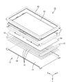
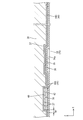
- FIG. 1 is an exploded perspective view showing a schematic configuration of a television receiver according to Embodiment 1 of the present invention.
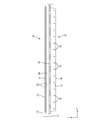
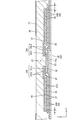
- the exploded perspective view which shows schematic structure of the liquid crystal display device with which a television receiver is equipped
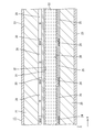
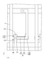
- Sectional drawing which shows schematically the cross-sectional structure of a liquid crystal display device
- Sectional drawing which shows the cross-sectional structure of a liquid crystal panel roughly
- the top view which shows the plane structure of the display area in the array substrate which comprises a liquid crystal panel
- a plan view showing a planar configuration in the vicinity of the TFT on the array substrate Sectional view along line vii-vii in FIG. Sectional view along the viii-vii line in FIG.
- FIG. 6 The top view which shows the state which patterned the resist apply
- FIG. 10 is an enlarged sectional view taken along line xiii-xii.
- 14 is an enlarged cross-sectional view along the xv-xv line in FIG.
- FIG. 16 is an enlarged cross-sectional view along the line xvii-xvii
- the top view which shows the plane structure of TFT vicinity in the array substrate which concerns on Embodiment 2 of this invention
- FIGS. 1 A first embodiment of the present invention will be described with reference to FIGS.
- a liquid crystal panel (display element) 11 constituting the liquid crystal display device 10 is illustrated.
- a part of each drawing shows an X axis, a Y axis, and a Z axis, and each axis direction is drawn to be a direction shown in each drawing.
- FIG. 1 is used as a reference, and the upper side of the figure is the front side and the lower side of the figure is the back side.
- the television receiver TV includes a liquid crystal display device (display device) 10, front and back cabinets Ca and Cb that are accommodated so as to sandwich the liquid crystal display device 10, a power supply P, A tuner T and a stand S are provided.
- the liquid crystal display device 10 has a horizontally long rectangular shape as a whole, and includes a liquid crystal panel 11 as a display panel and a backlight device (illumination device) 12 as an external light source, as shown in FIGS. Is integrally held by the bezel 13 or the like.
- the backlight device 12 is a so-called direct type in which a light source is disposed directly under the back surface of the liquid crystal panel 11.
- the backlight device 12 includes a chassis 14 opened on the front side (light emission side, liquid crystal panel 11 side), a reflective sheet (reflective member) 15 laid in the chassis 14, and an optical member attached to an opening portion of the chassis 14. 16, a frame 17 for fixing the optical member 16, a plurality of cold cathode tubes (light sources) 18 accommodated in parallel in the chassis 14, and an end portion of the cold cathode tube 18 while shielding light And a lamp holder 19 having light reflectivity.
- the liquid crystal panel 11 is formed by enclosing a liquid crystal layer 22 containing a liquid crystal material, which is a substance whose optical characteristics change with application of an electric field, between a pair of substrates 20 and 21.
- a liquid crystal material which is a substance whose optical characteristics change with application of an electric field.
- the array substrate display element, active matrix substrate
- the front side light emitting side.
- This is a CF substrate (counter display element, counter substrate) 21.
- a pair of front and back polarizing plates 23 are respectively attached to the outer surface sides of both the substrates 20 and 21.
- the array substrate 20 is formed by laminating a plurality of structures (thin films) on a substantially transparent (translucent) glass substrate GS. Specifically, on the inner surface side (the liquid crystal layer 22 side, the surface facing the CF substrate 21) of the glass substrate GS forming the array substrate 20, a switching element having three electrodes 24a to 24c as shown in FIG. A large number of TFTs (Thin Film Transistors) 24 and pixel electrodes 25 are provided side by side. Around the TFT 24 and the pixel electrodes 25, a grid-like gate wiring 26 and source wiring 27 are disposed so as to surround them. Has been.
- the pixel electrode 25 is made of a transparent conductive film such as ITO (Indium Tin Oxide).
- Both the gate wiring 26 and the source wiring 27 are made of a conductive material.
- the source wiring 27 has a two-layer structure in which different metal films 39 and 40 are laminated.
- the lower metal film 39 is made of titanium (Ti)
- the upper metal film is formed.
- 40 is made of aluminum (Al) (see FIG. 7). Since the lower layer metal film 39 contains titanium, the wiring resistance becomes low resistance, and since it is dense and has high mechanical strength, it can exhibit a high function as a barrier metal, thereby obtaining high connection reliability. be able to.
- the upper metal film 40 contains aluminum, the wiring resistance becomes low and the film formation and processing are easy.
- branch lines 26a and 27a extend from the vicinity of the intersecting portions of the gate line 26 and the source line 27 that intersect with each other, and part of these branch lines 26a and 27a.
- a gate electrode 24a and a source electrode 24b constituting the TFT 24 are configured by (the tip end side in the extending direction).
- the drain electrode 24c constituting the TFT 24 is formed on one end side of a drain wiring (pixel connection wiring) 34 described later.
- the array substrate 20 is provided with a capacitor wiring (auxiliary capacitor wiring, storage capacitor wiring, Cs wiring) 33 that is parallel to the gate wiring 26 and overlaps the pixel electrode 25 in a plan view.
- the capacity wiring 33 is alternately arranged with the gate wiring 26 in the Y-axis direction, and the interval between the adjacent gate wiring 26 and the capacity wiring 33 is set to be approximately equal.
- the gate wiring 26 is disposed between the pixel electrodes 25 adjacent to each other in the Y-axis direction, whereas the capacitor wiring 33 is disposed at a position that substantially crosses the central portion of each pixel electrode 25 in the Y-axis direction. Note that the source wiring 27, the gate wiring 26, and the capacitor wiring 33 that intersect with each other are kept in an insulated state by interposing the gate insulating film 35 therebetween.
- the end portion of the array substrate 20 is provided with a terminal portion routed from the gate wiring 26 and the capacitor wiring 33 and a terminal portion routed from the source wiring 27, and each of these terminal portions includes:
- Each signal or reference potential is input from an external circuit (not shown), and the driving of the TFT 24 is thereby controlled.
- An alignment film 28 for aligning liquid crystal molecules contained in the liquid crystal layer 22 is formed on the inner surface side of the array substrate 20.
- the CF substrate 21 is formed by laminating a structure on the plate surface of a glass substrate GS that is substantially transparent (having translucency) like the array substrate 20. Specifically, on the inner surface side (the liquid crystal layer 22 side, the surface facing the array substrate 20) of the glass substrate GS forming the CF substrate 21, as shown in FIG. A large number of color filters are arranged side by side at a position where they are superimposed on each other. In the color filter, the colored portions 29 exhibiting R (red), G (green), and B (blue) are arranged alternately along the X-axis direction. In addition, the outer shape of each colored portion 29 has a vertically long rectangular shape in plan view following the outer shape of the pixel electrode 25.
- each coloring part 29 which comprises a color filter
- the light-shielding part (black matrix) 30 which makes the grid
- the light shielding portion 30 is disposed so as to overlap with the gate wiring 26, the source wiring 27, and the capacitor wiring 33 on the array substrate 20 in plan view.
- a counter electrode 31 is provided on the surface of each colored portion 29 and the light shielding portion 30 so as to face the pixel electrode 25 on the array substrate 20 side.
- An alignment film 32 for aligning liquid crystal molecules contained in the liquid crystal layer 22 is formed on the inner surface side of the CF substrate 21.
- the TFT 24 which is a switching element among the structures of the array substrate 20 will be described in detail.
- the TFT 24 has a structure in which a plurality of thin films are sequentially stacked on the glass substrate GS forming the array substrate 20, and specifically, from the lower layer side (glass substrate GS side).
- a gate electrode 24a connected to the gate wiring 26, a gate insulating film 35, a semiconductor film 36, a doping semiconductor film 42, a source electrode 24b connected to the source wiring 27, a drain electrode 24c connected to the drain wiring 34, and an interlayer An insulating film (passivation film) 37 and a protective film 38 are stacked.
- the pixel electrode 25, the gate insulating film 35, the interlayer insulating film 37, and the protective film 38 are not shown.
- the gate electrode 24a is made of the same material as the gate wiring 26 and is patterned immediately above the glass substrate GS in the same process as the gate wiring 26.
- the gate electrode 24a extends from the vicinity of the intersection of the gate wiring 26 extending along the X-axis direction with the source wiring 27 along the Y-axis direction at the extending tip of the branch line 26a. It consists of parts.
- the gate insulating film 35 is made of, for example, a silicon nitride film (SiNx), and as shown in FIG. 7, the gate electrode 24a and the semiconductor film 36 described below are kept in an insulating state.
- the gate insulating film 35 has a solid pattern that covers not only the TFT 24 formation region but also the entire surface of the glass substrate GS.
- the semiconductor film 36 is made of, for example, amorphous silicon (a-Si). One end side is connected to the source electrode 24b and the other end side is connected to the drain electrode 24c. Have. As shown in FIG. 6, the semiconductor film 36 has a smaller dimension in the Y-axis direction (a direction perpendicular to the arrangement direction of the source electrode 24b and the drain electrode 24c) than the gate electrode 24a. 24b and the drain electrode 24c are larger.
- the doped semiconductor film 42 is made of amorphous silicon (n + Si) doped with an n-type impurity such as phosphorus (P) at a high concentration.
- the doping semiconductor film 42 extends along the semiconductor film 36 but is removed with respect to the range of the channel region CH, and a pair of portions arranged with the channel region CH interposed therebetween are a source electrode 24b and a drain described below. It constitutes a part of the electrode 24c.
- the dimension of the doping semiconductor film 42 in the Y-axis direction is substantially the same as that of the source electrode 24b and the drain electrode 24c.
- the source electrode 24 b and the drain electrode 24 c include the same material as the source wiring 27 and the drain wiring 34 and are patterned on the glass substrate GS in the same process as the source wiring 27 and the drain wiring 34. As shown in FIGS. 6 and 7, the source electrode 24 b and the drain electrode 24 c are arranged to face each other with a predetermined interval in the X-axis direction. The source electrode 24b and the drain electrode 24c are disposed on the upper layer side with respect to the gate electrode 24a via the gate insulating film 35 and the semiconductor film 36, respectively, and a part (opposing portion) of the source electrode 24b and the drain electrode 24c is planar with respect to the gate electrode 24a. The overlapping portion is placed on the gate electrode 24a. As shown in FIG.
- the source electrode 24b and the drain electrode 24c are composed of a first conductive film 24b1, 24c1 on the lower layer side (semiconductor film 36 side) and a second conductive film 24b2, on the upper layer side (interlayer insulating film 37 side). 24c2 is laminated.
- the first conductive films 24b1 and 24c1 on the lower layer side are respectively constituted by the end portions of the doping semiconductor film 42 described above, and function as ohmic contact layers that are in ohmic contact with the semiconductor film 36 on the lower layer side. is there.
- the second conductive films 24b2 and 24c2 on the upper layer side have a two-layer structure in which different metal films are laminated, and the metal film 39 on the lower layer side is made of titanium (Ti), whereas the metal on the upper layer side is made.
- the film 40 is made of aluminum (Al). That is, the source electrode 24b and the drain electrode 24c are common to the source wiring 27 in that they have the second conductive films 24b2 and 24c2 made of two metal films 39 and 40.
- the structure differs from the source wiring 27 in that the first conductive films 24b1 and 24c1 are provided.
- the source wiring 27 includes only the second conductive films 24b2 and 24c2 (39, 40) of the source electrode 24b and the drain electrode 24c, and does not have the first conductive films 24b1 and 24c1 (42). However, these are different in configuration. Further, as shown in FIG. 6, the source electrode 24b extends along the branch line 27a extending along the X-axis direction from the vicinity of the intersection with the gate wiring 26 in the source wiring 27 extending along the Y-axis direction. It is comprised by the protrusion front-end
- the source electrode 24b and the drain electrode 24c are arranged to face each other with a predetermined interval therebetween, and thus are not directly electrically connected to each other.
- the source electrode 24b and the drain electrode 24c are indirectly electrically connected via the semiconductor film 36 on the lower layer side, and the bridge portion between the electrodes 24b and 24c in the semiconductor film 36 has a drain current. It functions as a flowing channel region CH.
- the source electrode 24b and the drain electrode 24c are symmetrical with each other.
- the interlayer insulating film 37 is made of, for example, a silicon nitride film (SiNx), and is made of the same material as the gate insulating film 35 described above.
- the protective film 38 is made of an acrylic resin (for example, polymethyl methacrylate resin (PMMA)) or a polyimide resin, which is an organic material. Therefore, the protective film 38 is thicker than the gate insulating film 35 and the interlayer insulating film 37 made of other inorganic materials and functions as a planarizing film. Both the interlayer insulating film 37 and the protective film 38 have a solid pattern extending over almost the entire surface of the glass substrate GS as well as the region where the TFT 24 is formed.
- the interlayer insulating film 37 and the protective film 38 are disposed between the source wiring 27, the drain wiring 34, and the contact portion 41 on the relatively lower layer side and the pixel electrode 25 on the relatively upper layer side outside the region where the TFT 24 is formed. It is assumed that they are interposed and kept in an insulated state.
- the drain wiring 34 connected to the drain electrode 24c is substantially L-shaped in plan view as shown in FIG. 6, and one end side of the drain wiring 34 is connected to the drain electrode 24c. The other end is connected to a contact portion 41 that is in contact with the pixel electrode 25.
- the drain wiring 34 extends from the drain electrode 24c along the X-axis direction, is then bent toward the capacitor wiring 33 side, and extends along the Y-axis direction, thereby connecting to the contact portion 41.
- the drain wiring 34 is formed on the gate insulating film 35, is made of the same material as the source wiring 27, and has the same two-layer structure.
- the drain wiring 34 is composed of only the second conductive films 24b2 and 24c2 (39, 40) of the source electrode 24b and the drain electrode 24c, as in the case of the source wiring 27, and the first conductive films 24b1, 24c1 (42). It differs from these in that it does not have.
- the contact portion 41 is arranged at a position that overlaps the capacitive wiring 33 that is a light shielding region in a plan view. Accordingly, as the structure for contacting the pixel electrode 25 with the contact portion 41 is formed, irregularities are formed on the surfaces of the pixel electrode 25 and the alignment film 28, which causes the alignment of the liquid crystal molecules contained in the liquid crystal layer 22. Even when the state is disturbed, the occurrence of light leakage can be avoided.
- the contact portion 41 has a horizontally long rectangular shape along the extending direction (X-axis direction) of the capacitor wiring 33 when viewed in plan, and the short side dimension is narrower than the wiring width of the capacitor wiring 33.
- the contact portion 41 is connected to the other end of the drain wiring 34, that is, the end opposite to the drain electrode 24c side, and the left side (shown in FIG. 6) along the X-axis direction from the end of the drain wiring 34. It is arranged so as to protrude to the TFT 24 side.
- the contact portion 41 is made of the same material as the source wiring 27 and the drain wiring 34 described above, and is patterned on the glass substrate GS in the same process as the source wiring 27 and the drain wiring 34.
- the contact portion 41 is formed on the gate insulating film 35, and an interlayer insulating film 37, a protective film 38, and the pixel electrode 25 are stacked in that order on the upper layer side. In the interlayer insulating film 37 and the protective film 38, a contact hole 43 is formed at a position overlapping the contact portion 41 in plan view, and the pixel electrode 25 is connected to the contact portion 41 through the contact hole 43. Connected.
- the semiconductor film 36 and the doping semiconductor film 42 are viewed in plan with respect to the source wiring 27 and the drain wiring 34 as shown in FIG.
- semiconductor film extending portions 44 extending to the overlapping range are formed.
- the semiconductor film extending portion 44 is formed by extending the semiconductor film 36 and the doping semiconductor film 42 and is made of the same material as that of the semiconductor film 36 and the doping semiconductor film 42 and is patterned in the same process.
- the semiconductor film extending portion 44 has a two-layer structure including an extended portion of the lower semiconductor film 36 and an extended portion of the upper doped semiconductor film 42.
- the semiconductor film extending portion 44 is connected to the source wiring 27 from both ends of the semiconductor film 36 and the doping semiconductor film 42 opposite to the channel region CH side in the X-axis direction (alignment direction of the source electrode 24b and the drain electrode 24c). A pair is formed so as to extend along the drain wiring 34.
- the semiconductor film extending portion 44 has the same dimension in the Y-axis direction in the portion extending along the X-axis direction from the end portions of the semiconductor film 36 and the doping semiconductor film 42, and the same dimension of the semiconductor film 36 in the formation region of the TFT 24. It is relatively small.
- first semiconductor film extending portion what is superimposed on the source wiring 27 is referred to as a “first semiconductor film extending portion”, and a suffix A is added to the drain wiring 34.
- second semiconductor film extending portion the superimposing part is added as a “second semiconductor film extending portion” with a subscript B, and when referring generically without distinction, the subscript is not added.
- the first semiconductor film extending portion 44A includes, as shown in FIGS. 6 and 7, the semiconductor film 36 and the doping semiconductor film 42 and the end portion of the source electrode 24b. Is further extended along the branch line 27a (X-axis direction) of the source wiring 27 toward the left side (the main body side of the source wiring 27) shown in FIGS. 6 and 7, thereby lower layer side with respect to the branch line 27a. It is arranged to overlap. Since the first semiconductor film extending portion 44A is constituted by extending portions of the semiconductor film 36 and the doping semiconductor film 42, the branch line 27a of the source wiring 27 stacked thereon is connected to the source electrode 24b. In this way, the connection is made in a flat state without any step.
- the first semiconductor film extending portion 44A When the first semiconductor film extending portion 44A reaches the main body of the source wiring 27 (the trunk line excluding the branch line 27a), it further extends vertically along the main body of the source wiring 27 in the Y-axis direction as shown in FIG. As a result, the main body of the source wiring 27 is arranged so as to overlap with the lower layer side.
- the first semiconductor film extending portion 44 ⁇ / b> A is formed over a range that overlaps the substantially entire area of the main body of the source wiring 27 in a plan view. That is, the first semiconductor film extending portion 44A is formed over a range that overlaps almost the entire area of the source wiring 27 including the branch line 27a in a plan view.
- the first semiconductor film extending portion 44A is present over almost the entire area on the lower layer side of the main body of the source wiring 27, whereby the source wiring 27 is located over the entire area than the first semiconductor film extending portion 44A. There is no contact with the gate insulating film 35 on the lower layer side, and no step is caused.
- the first semiconductor film extension 44 ⁇ / b> A is formed over a wider area than the overlapping source wiring 27 (including the branch line 27 a) in a plan view.
- the size (area) is relatively large.
- the extended portion of the lower semiconductor film 36 in the first semiconductor film extending portion 44 ⁇ / b> A has both outer edges extending substantially along the extending direction as shown in FIGS. 6 to 9. 27 is arranged outside the both outer edges.
- the extended portion of the semiconductor film 36 on the lower layer side of the first semiconductor film extending portion 44A has the center position in the width direction substantially coincided with the center position in the width direction of the source wiring 27, and each outer edge and the source wiring
- the distance (width of non-overlapping portion) D1 between the 27 corresponding outer edges is substantially equal (see FIGS. 7 and 9).
- the extended portion of the upper doped semiconductor film 42 in the first semiconductor film extending portion 44A has substantially the same line width as the source wiring 27 and may protrude from both outer edges when seen in a plan view. Not supposed to be.
- the second semiconductor film extending portion 44B of the pair of semiconductor film extending portions 44 is formed by further separating the semiconductor film 36 and the doping semiconductor film 42 from the end of the drain electrode 24c. It is formed so as to extend in parallel with the wiring 34, and has a bent shape that is substantially L-shaped in a plan view as in the case of the drain wiring 34. Thereby, the second semiconductor film extension 44 ⁇ / b> B is disposed so as to overlap the lower layer side of the drain wiring 34. Since the second semiconductor film extending portion 44B is constituted by extending portions of the semiconductor film 36 and the doping semiconductor film 42, the drain wiring 27 stacked thereon has a step in the middle of the drain electrode 24c.
- the second semiconductor film extension 44 ⁇ / b> B is formed over a range that overlaps almost the entire area of the drain wiring 34 in a plan view. Further, the second semiconductor film extending portion 44B is configured to extend to a range overlapping with the contact portion 41 connected to the end portion of the drain wiring 34 when viewed in a plane. Specifically, the end of the second semiconductor film extending portion 44B opposite to the drain electrode 24c side protrudes toward the left side shown in FIG. The second semiconductor film extending portion 44 ⁇ / b> B is formed over a range that overlaps substantially the entire region of the contact portion 41 in a plan view.
- the second semiconductor film extending portion 44B is present over almost the entire region on the lower layer side of the drain wiring 34 and the contact portion 41, whereby the drain wiring 34 and the contact portion 41 are disposed over the entire region of the second semiconductor film. There is no contact with the gate insulating film 35 on the lower layer side than the extending portion 44B, and no step is caused accordingly.
- the second semiconductor film extension 44 ⁇ / b> B is formed over a wider area in a plan view than the overlapping drain wiring 34 and the contact part 41, and has a size (see in a plan view). Area) is relatively larger than these.
- the overlapping portion with the drain wiring 34 has both outer edges along the extending direction as shown in FIG. Is disposed outside the outer edges of the drain wiring 34.
- the outer peripheral edge of the overlapping portion with the contact portion 41 is arranged outside the outer peripheral edge of the contact portion 41.
- the extended portion of the semiconductor film 36 on the lower layer side in the second semiconductor film extending portion 44B has its outer peripheral edge disposed almost outside the both outer edges of the drain wiring 34 and the outer peripheral edge of the contact portion 41. .
- the overlapping portion with the drain wiring 34 is substantially coincident with the central position in the width direction of the drain wiring 34.
- the distances (widths of non-overlapping portions) D1 between the outer edges and the corresponding outer edges of the drain wiring 34 are substantially equal.
- This distance D1 is equal to the distance D1 between each outer edge of the extended portion of the semiconductor film 36 on the lower layer side in the first semiconductor film extending portion 44A described above and each corresponding outer edge of the source wiring 27. (See FIGS. 6, 7 and 9).
- the overlapping portion with the contact portion 41 has a center position substantially coincident with the center position of the contact portion 41, The distance from the outer peripheral edge of the contact portion 41 (the width of the non-overlapping portion) is substantially equal over the entire circumference.
- This distance is the distance D1 between each outer edge of the extended portion of the semiconductor film 36 on the lower layer side in the first semiconductor film extension 44A described above and each corresponding outer edge of the source wiring 27, and the second semiconductor film extension.
- the distance D1 between each outer edge of the overlapping portion of the existing portion 44B with the drain wiring 34 and each corresponding outer edge of the drain wiring 34 is set (see FIG. 6). That is, the semiconductor film extension 44 according to the present embodiment has a distance (non-overlapping) between the outer periphery and the outer periphery of the structure (source wiring 27, drain wiring 34, and contact part 41) to be superimposed.
- the width (D1) of the portion is substantially the same over the entire area.
- the extension portion of the upper semiconductor layer 42 in the second semiconductor film extension portion 44B has substantially the same size as the drain wiring 27 and the contact portion 41 in plan view, and is seen in plan view.
- the drain wiring 27 and the contact portion 41 do not protrude from the outer edges.
- This embodiment has the structure as described above, and its operation will be described next.
- the manufacturing procedure of the array substrate 20 in the liquid crystal panel 11 will be described in detail.
- Each structure is sequentially stacked on the plate surface of the glass substrate GS forming the array substrate 20 by a known photolithography method. Specifically, first, the gate electrode 24a, the gate wiring 26, and the capacitor wiring 33 as the first layer are patterned on the surface of the glass substrate GS using a predetermined photomask, and then the gate insulation as the second layer. A film 35 is formed, and the semiconductor film 36 as the third layer and the doping semiconductor film 42 as the fourth layer are patterned using a predetermined photomask. At this time, the semiconductor film extending portion 44 constituted by the extended portions of the semiconductor film 36 and the doping semiconductor film 42 is extended to the formation planned range of the source wiring 27, the drain wiring 34, and the contact portion 41. .
- the source electrode 24b and the drain electrode 24c are composed of a fourth layer (doping semiconductor film 42) and a fifth layer (metal films 39 and 40).
- a semiconductor material film made of the material of the semiconductor film 36 and a doping semiconductor material film made of the material of the doping semiconductor film 42 are sequentially formed on the glass substrate GS patterned with the second layer, and the upper layer side A resist is further applied on the solid doped semiconductor material film. After the applied resist is exposed through a predetermined photomask and the resist is developed, the semiconductor material film and the doped semiconductor material film are subsequently etched (for example, dry etching), whereby the semiconductor film 36 having a predetermined pattern is obtained. Then, the doping semiconductor film 42 and the semiconductor film extending portion 44 are formed.
- an extended portion of the doping semiconductor film 42 constituting the doping semiconductor film 42 and the semiconductor film extending portion 44 is an extended portion of the semiconductor film 36 and the semiconductor film 36 constituting the semiconductor film extending portion 44 in a plan view. And the same pattern shape (same size in plan view).
- the upper layer metal material film M2 made of aluminum which is the material of the side metal film 40 is formed, a resist R is applied on the solid upper layer metal material film M2.
- the applied resist R is exposed to light through a predetermined photomask and then developed, so that the pattern shown in FIG. 10 is obtained.
- the remaining formation range of the resist R coincides with the planned formation range of the source electrode 24b, the drain electrode 24c, the source wiring 27, the drain wiring 34, and the contact portion 41.
- the shaded range is the formation range of the patterned resist R.
- the solid gate insulating film 35, the lower metal material film M1, and the upper metal material film M2 are not shown.
- the metal material films M1 and M2 are etched using the resist R as a mask.
- an etching solution is supplied to the glass substrate GS to etch portions of the metal material films M1 and M2 that are not covered with the resist R. Remove by corrosive dissolution with liquid.
- the etching range in each of the metal material films M1 and M2 is theoretically coincident with an uncovered region that is not covered with the resist R.
- the resist Even if it is a covered region by R, there is a possibility that the etching solution that has penetrated into the adjacent non-covered region penetrates beyond the boundary and is over-etched.
- substrate in each metal material film M1, M2 can change with the presence or absence of a level
- the thickness of the semiconductor film and the doping semiconductor film is added to each metal material film stacked thereon. Since a step with the combined height is generated, the adhesion between the metal material films and the adhesion between the lower metal material film and the gate insulating film may be significantly deteriorated at the step. As a result, over-etching with an etching solution is likely to occur, and the line width becomes narrower than planned or disconnection is likely to occur. In this regard, in the present embodiment, as shown in FIGS.
- each of the metal material films M1 and M2 is disposed on the semiconductor film 36, the doping semiconductor film 42, and the semiconductor film extending portion 44 that is an extension thereof over almost the entire area.
- the metal material films M1 and M2 do not have a level difference caused by the semiconductor film 36 and the doping semiconductor film 42 as in the prior art, and thereby have relatively good adhesion to the base. It has become.
- each of the metal material films M1 and M2 can be accurately etched according to the pattern of the resist R, the boundary position between the source electrode 24b and the source wiring 27 formed by the etching, the drain electrode 24c and the drain wiring 34. It is possible to effectively prevent the line width from being narrowed or disconnection from occurring at the boundary position. Thereby, high connection reliability can be obtained, and the operational reliability of the TFT 24 and the reliability related to the display of the liquid crystal display device 10 can both be improved.
- a disconnection occurs in the middle of the source wiring 27, it can be remedied by a wiring repair means such as a spare wiring (not shown), whereas the boundary position between the source electrode 24b and the source wiring 27
- a wiring repair means such as a spare wiring (not shown)
- the boundary position between the source electrode 24b and the source wiring 27 there is a circumstance that such relief is extremely difficult.
- the semiconductor film extending portion 44 since the semiconductor film extending portion 44 according to the present embodiment extends to a range overlapping in plan view over almost the entire area of the source wiring 27, the drain wiring 34, and the contact portion 41, the source wiring 27. The occurrence of disconnection or the like can be prevented in almost the entire region of the drain wiring 34 and the contact portion 41, and the connection reliability can be further improved.
- each metal material film M1, M2 there are cases where dry etching and wet etching are performed before and after the time. In this case, only the upper metal material film M2 is selectively etched by wet etching. Even in such a case, the same effect as described above, that is, the effect of preventing disconnection of the upper metal material film M2 can be obtained.
- the doping semiconductor film 42 (including the extended portion of the doping semiconductor film 42 in the semiconductor film extending portion 44) is continuously etched, and then the upper layer side metal material The resist R on the film M2 is peeled off. Thereby, the doping semiconductor film 42 can be separated into the left and right sides with an interval corresponding to the channel region CH of the semiconductor film 36.
- the interlayer insulating film 37 as the sixth layer and the protective film 38 as the seventh layer are successively formed. These are formed into a film and patterned in a lump.
- the alignment film 28 is further formed thereon, whereby the manufacture of the array substrate 20 is completed.
- the manufactured array substrate 20 is bonded to a separately manufactured CF substrate 21 with the liquid crystal layer 22 interposed therebetween, whereby the liquid crystal panel 11 shown in FIG. 4 is obtained.
- the manufactured liquid crystal panel 11 is assembled to the backlight device 12 via the bezel 13, whereby the liquid crystal display device 10 shown in FIGS. 2 and 3 is obtained.
- a third layer (semiconductor film 36) and a fourth layer (doping semiconductor film 42), and a fifth layer (source wiring 27, drain) are formed. Since the wiring 34 and the contact portion 41) are patterned by using different photomasks, depending on the exposure accuracy, the position is shifted from the normal position (designed position) in the direction along the plate surface of the array substrate 20. May be formed. However, in the present embodiment, the extended portions of the semiconductor film 36 in the semiconductor film 36 and the semiconductor film extending portion 44 are viewed in a plane more than the source electrode 24b, the drain electrode 24c, the source wiring 27, the drain wiring 34, and the contact portion 41.
- the difference in size (distance D1, margin) in a plan view between the extended portion of the semiconductor film 36 in the semiconductor film extending portion 44 and the source wiring 27, the drain wiring 34, and the contact portion 41 is determined in the manufacturing apparatus.
- a relatively small source wiring 27, drain wiring 34, and contact portion 41 with respect to the extended portion of the semiconductor film 36 in the relatively large semiconductor film extending portion 44 Even when the position is displaced in the Y-axis direction, the amount of displacement is not designed to exceed the distance D1, so that the source wiring 27, the drain wiring 34, and the contact portion 41 include the semiconductor film extending portion 44.
- the semiconductor film 36 is located on the inner side of the outer edges of the extended portion of the semiconductor film 36, and the situation of protruding outward from either of the outer edges is reliably avoided. Further, as shown in FIGS.
- the relatively small source wiring 27, drain wiring 34, and contact portion 41 with respect to the extended portion of the semiconductor film 36 in the relatively large semiconductor film extending portion 44 are connected to the X axis. Even when the position is displaced in the direction, since the amount of displacement is not designed to exceed the distance D1, the source wiring 27, the drain wiring 34, and the contact portion 41 are formed in the semiconductor film extending portion 44. It exists in the inner side rather than the both outer edges of the extension part of 36, and the situation which protrudes outside from either of both outer edges is avoided reliably. Accordingly, the extension of the semiconductor film 36 in the semiconductor film extension 44 and the overall size of the source wiring 27, drain wiring 34, and contact part 41 are relatively wide in size.
- the extended portion of the semiconductor film 36 at 44 is dominant, and even if the source wiring 27, the drain wiring 34, and the contact portion 41 are displaced, they hardly change and are always kept constant. As a result, the extended portion of the semiconductor film 36 in the semiconductor film extending portion 44, both of which are conductors, and the source wiring 27, the drain wiring 34, and the contact portion 41 are formed between other wirings such as the capacitor wiring 33, for example. It is avoided that the capacitance value to be changed fluctuates. If the capacitance value formed between the capacitor wiring 33 and the capacitor wiring 33 is stabilized, it is possible to avoid fluctuations in the voltage value charged in the pixel electrode 25 forming a capacitor with the capacitor wiring 33. Accordingly, it is possible to avoid variation in the gradation value of the display image displayed based on the voltage value charged in the pixel electrode 25 and to obtain a good display quality.
- the array substrate (display element) 20 of the present embodiment includes the glass substrate (substrate) GS, the gate wiring 26 formed on the glass substrate GS, and the gate electrode 24a formed on the gate wiring 26.
- Drain electrode 24c formed in the semiconductor film 36 and extending to at least a portion overlapping the source wiring 27 in plan view. And a Makunobezai portion 44.
- the source electrode 24b and the drain electrode 24c are provided between them.
- a drain current flows through the channel region CH of the semiconductor film 36.
- the semiconductor film extending portion 44 is formed on the semiconductor film 36 so as to extend to a range overlapping at least a part of the source wiring 27 in plan view, the source electrode 24b and the source wiring 27 are formed. It is possible to avoid a step due to the semiconductor film 36 between the two.
- connection reliability can be improved.
- the semiconductor film extending portion 44 extends to a range overlapping with almost the entire area of the source wiring 27 in a plan view. By doing so, it is possible to prevent disconnection or the like caused by the semiconductor film 36 in almost the entire area of the source wiring 27, and therefore connection reliability can be further improved.
- the semiconductor film extending portion 44 is formed so as to be larger than the source wiring 27 in a plan view. Even if the semiconductor film extending portion 44 and the source wiring 27 are displaced in one direction along the planar direction due to the influence of an accuracy error or the like that may occur in manufacturing, the semiconductor film extending portion 44 is not connected to the source wiring. 27 when viewed from the plane, so that when the amount of positional deviation is within the range of the difference in size in one direction, the semiconductor film extension 44 and the source wiring 27 are viewed from the plane. Variations in the overall size can be avoided. This makes it difficult for the semiconductor film extension 44 and the source wiring 27 to change in the value of the capacitance formed with other wirings, thereby avoiding a situation in which electrical adverse effects are caused.
- the semiconductor film extension 44 and the source wiring 27 can change in the value of the capacitance formed with other wirings, thereby avoiding a situation in which electrical adverse effects are caused.
- the semiconductor film extending portion 44 has both outer edges arranged outside the both outer edges of the source wiring 27. In this way, even when the semiconductor film extending portion 44 and the source wiring 27 are displaced in one direction along the plane direction, the situation where the source wiring 27 protrudes from either of the outer edges of the semiconductor film 36 occurs. Can be prevented.
- the source electrode 24b and the drain electrode 24c are each a stacked structure of a doping semiconductor film 42 formed on the semiconductor film 36 to which impurities are added and metal films 39 and 40 formed on the doping semiconductor film 42 and made of a metal material.
- the source wiring 27 is made of the same material as the metal films 39 and 40 constituting the source electrode 24b, and the semiconductor film extending portion 44 is an end of the doping semiconductor film 42. From the portion to the source wiring 27 side. In this way, the metal films 39 and 40 forming the source electrode 24 b and the drain electrode 24 c are in ohmic contact with the semiconductor film 36 by the doping semiconductor film 42.
- the semiconductor film extension 44 extends from the end of the doping semiconductor film 42 to the source wiring 27 side, the ends of the doping semiconductor film and the semiconductor film are aligned as in the conventional case.
- the step formed is a film of the doping semiconductor film 42. Only the thickness is sufficient. Thereby, disconnection etc. can be made hard to occur and high connection reliability can be obtained.
- the drain electrode 34 formed on the pixel electrode 25 and the gate insulating film 35 and having one end connected to the drain electrode 24 c and the other end of the drain interconnect 34 and connected to the pixel electrode 25.
- the semiconductor film extending portion 44 extends to a range that overlaps at least a part of the drain wiring 34 in a plan view. In this way, based on the scanning signal and the data signal supplied to the gate wiring 26 and the source wiring 27, respectively, the pixel electrode 25 is connected to the pixel electrode 25 through the drain wiring 34 and the contact portion 41 connected to the drain electrode 24c. The voltage can be charged.
- the semiconductor film extending portion 44 extends to a range that overlaps at least a portion of the drain wiring 34 in a plan view, the semiconductor film 36 is formed between the drain electrode 24 c and the drain wiring 34. It is possible to avoid the resulting level difference. As a result, disconnection or the like hardly occurs when wet etching is performed on the drain electrode 24c and the drain wiring 34 in the manufacturing process, and thus high connection reliability can be obtained.
- the semiconductor film extending portion 44 extends to a range that overlaps with almost the entire area of the drain wiring 34 in a plan view. In this way, it is possible to prevent disconnection or the like due to the semiconductor film 36 in almost the entire region of the drain wiring 34, and to further improve connection reliability.
- the semiconductor film extending portion 44 is formed to be larger than the drain wiring 34 in a plan view. Even if the semiconductor film extension 44 and the drain wiring 34 are misaligned in one direction along the plane direction due to the influence of an accuracy error that may occur in the manufacturing process, the semiconductor film extension 44 is not connected to the drain wiring. When the amount of positional deviation is within the range of the difference in size in one direction, the semiconductor film extension 44 and the drain wiring 34 are viewed in a plane. Variations in the overall size can be avoided. This makes it difficult for the semiconductor film extension 44 and the drain wiring 34 to change in the value of the capacitance formed between the semiconductor wiring extension 44 and the drain wiring 34 and the like, thereby avoiding a situation where an electrical adverse effect is caused.
- the semiconductor film extension 44 and the drain wiring 34 can change in the value of the capacitance formed between the semiconductor wiring extension 44 and the drain wiring 34 and the like, thereby avoiding a situation where an electrical adverse effect is caused.
- the semiconductor film extending portion 44 has both outer edges arranged outside the both outer edges of the drain wiring 34. In this way, even when the semiconductor film extending portion 44 and the drain wiring 34 are displaced in one direction along the plane direction, the situation where the drain wiring 34 protrudes from either of the outer edges of the semiconductor film 36 occurs. Can be prevented.
- the semiconductor film extending portion 44 extends to a range overlapping with almost the entire area of the contact portion 41 in a plan view. In this way, it is possible to prevent disconnection or the like due to the semiconductor film 36 in almost the entire contact portion 41 in addition to the drain wiring 34, and the connection reliability can be further improved.
- the semiconductor film extending portion 44 is formed larger than the contact portion 41 in a plan view. Even if the semiconductor film extending portion 44 and the contact portion 41 are misaligned in one direction along the plane direction due to the influence of an accuracy error that may occur in manufacturing, the semiconductor film extending portion 44 is in contact with the contact portion. 41 is larger than 41 in a plan view, and if the amount of positional deviation is within the range of the difference in size in one direction, the semiconductor film extension 44 and the contact portion 41 are viewed in a plane. Variations in the overall size can be avoided. As a result, the semiconductor film extending portion 44 and the contact portion 41 are less likely to change in the value of the capacitance formed between other wirings and the like, thereby avoiding a situation where an electrical adverse effect is caused.
- the semiconductor film extending portion 44 and the contact portion 41 are less likely to change in the value of the capacitance formed between other wirings and the like, thereby avoiding a situation where an electrical adverse effect is caused.
- the outer peripheral edge of the semiconductor film extending portion 44 is arranged outside the outer peripheral edge of the contact portion 41. In this case, even when the semiconductor film extending portion 44 and the contact portion 41 are displaced in one direction along the plane direction, the contact portion 41 protrudes from any one of the outer peripheral edges of the semiconductor film 36. Can be prevented.
- the semiconductor film extending portion 144 is configured to extend to a range overlapping each part of the source wiring 27 and the drain wiring 34 in a plan view. ing. Specifically, the first semiconductor film extension portion 144A extends along the X-axis direction from the end portion on the source electrode 24b side in the semiconductor film 136 and the doping semiconductor film (not shown) toward the main body of the source wiring 27. At the same time, it overlaps the entire area of the branch line 27a in the source wiring 27 and the connection portion of the branch line 27a in the main body in a plan view.
- the first semiconductor film extending portion 144A is in a relationship that does not overlap in plan view with respect to most of the main body of the source wiring 27 except for the connection portion of the branch line 27a.
- the second semiconductor film extending portion 144B extends along the X-axis direction along the drain wiring 34 from the end on the drain electrode 24c side in the semiconductor film 136 and the doping semiconductor film. 34, the first portion 34a along the X-axis direction overlaps substantially the entire region in a plan view. Accordingly, the second semiconductor film extending portion 144B is in a relationship that does not overlap in a plan view with respect to almost the entire area of the second portion 34b along the Y-axis direction in the drain wiring 34.
- the second semiconductor film extending portion 144B avoids the occurrence of a step due to the semiconductor film 136 and the doping semiconductor film. It is possible to effectively prevent the width from narrowing or disconnection.
- the first semiconductor film extending portion extends over a range that overlaps a part of the source wiring in plan view.
- the general formation range can be changed as appropriate.
- the first semiconductor film extension is formed so as to overlap in plan view with the whole area of the branch line of the source wiring and a predetermined length portion including the connection part of the branch line in the main body of the source wiring. It can be a range.
- the first semiconductor film extending portion may be formed so as to overlap with only a part of the branch line of the source wiring in a plan view and not to overlap with the main body of the source wiring in a plan view.
- the second semiconductor film extending portion extends over a range overlapping in plan view with respect to a part of the drain wiring.
- the general formation range can be changed as appropriate.
- the extended portion of the second semiconductor film overlaps the entire area of the drain wiring in a plan view, but can be a formation range that does not overlap the contact portion in a plan view.
- the second semiconductor film extending portion may be a formation range that overlaps the entire area of the first portion of the drain wiring and a part of the second portion in plan view.
- the second semiconductor film extending portion is overlapped in plan view only on a part of the first portion of the drain wiring, and is not overlapped in plan view with the second portion of the drain wiring and the remaining portion of the first portion. It can also be a range.
- the second semiconductor film extending portion may be a formation range that overlaps the entire area of the drain wiring and a part of the contact portion in plan view.
- the semiconductor film extension portion and the source wiring, the drain wiring, and the contact portion are arranged so as to be substantially concentric at the normal position (designed position). It is also possible to adopt a configuration in which is eccentrically arranged.
- one outer edge of the first semiconductor film extending portion is arranged so as to be flush with one outer edge of the source wiring, or the second semiconductor film extending. It is also possible to arrange such that one outer edge in the portion is flush with one outer edge of the drain wiring and one outer edge of the contact portion.
- the first semiconductor film extension portion is shown to have a size over a wide range as viewed in plan than the source wiring.
- the semiconductor film extension portion is the source wiring Those formed in the same size in a plan view are also included in the present invention. This relationship can be similarly applied to the second semiconductor film extending portion, the drain wiring, and the contact portion.
- the outer edge of the semiconductor film extending portion is configured to be arranged outside the outer edges of the source wiring, the drain wiring, and the contact portion. It is also possible to adopt a configuration in which the outer edge is arranged inside the outer edge of at least one of the source wiring, the drain wiring, and the contact portion.
- the drain wiring that connects the contact portion and the drain electrode is exemplified.
- the drain wiring can be omitted as a configuration in which the contact portion is provided on the drain electrode. .
- the present invention can be applied even in such a configuration.
- the second semiconductor film extending portion can be removed. Even in such a case, by providing the first semiconductor film extending portion that overlaps the source wiring in plan view, an effect of preventing disconnection that may occur in the source wiring can be obtained.
- the metal film on the upper layer side constituting the source wiring, drain wiring, contact portion and the like is made of aluminum.
- aluminum for example, molybdenum (Mo) or copper ( Cu) or the like can also be used.
- the metal film on the lower layer side constituting the source wiring, drain wiring, contact portion and the like has been shown to contain titanium, but other than titanium, for example, chromium (Cr), tantalum ( It is also possible to use Ta), copper (Cu), or the like.
- the direct type is exemplified as the backlight device included in the liquid crystal display device, but the present invention includes a backlight device of an edge light type.
- a transmissive liquid crystal display device including a backlight device that is an external light source is exemplified.
- the present invention is applied to a reflective liquid crystal display device that performs display using external light.
- the backlight device can be omitted.
- a TFT is used as a switching element of a liquid crystal display device.
- the present invention can also be applied to a liquid crystal display device using a switching element other than TFT (for example, a thin film diode (TFD)).
- a switching element other than TFT for example, a thin film diode (TFD)
- the present invention can also be applied to a liquid crystal display device for monochrome display.
- the liquid crystal display device using a liquid crystal panel as the display panel has been exemplified.
- the present invention is applicable to a display device using another type of display panel (PDP, organic EL panel, etc.). Applicable. In that case, the backlight device can be omitted.
- SYMBOLS 10 Liquid crystal display device (display device), 12 ... Backlight device (illumination device), 20 ... Array substrate (display element), 21 ... CF substrate (counter display element), 24a ... Gate electrode, 24b ... Source electrode, 24c DESCRIPTION OF SYMBOLS ... Drain electrode, 25 ... Pixel electrode, 26 ... Gate wiring, 27 ... Source wiring, 34 ... Drain wiring, 35 ... Gate insulating film, 36 ... Semiconductor film, 39 ... Lower layer side metal film (metal film), 40 ... Upper layer Side metal film (metal film), 41 ... contact part, 42 ... doping semiconductor film, 44,144 ... semiconductor film extension part, CH ... channel region, GS ... glass substrate (substrate), TV ... TV receiver
Landscapes
- Physics & Mathematics (AREA)
- Nonlinear Science (AREA)
- Engineering & Computer Science (AREA)
- Microelectronics & Electronic Packaging (AREA)
- Mathematical Physics (AREA)
- Chemical & Material Sciences (AREA)
- Crystallography & Structural Chemistry (AREA)
- General Physics & Mathematics (AREA)
- Optics & Photonics (AREA)
- Liquid Crystal (AREA)
- Thin Film Transistor (AREA)
Abstract
Un substrat de matrice (20) est pourvu: d'un substrat en verre (GS) ; d'un câblage de grille (26) formé sur le substrat de verre (GS) ; d'une électrode de grille (24a) formée sur le câblage de grille (26) ; d'un film d'isolation de grille (35) formé sur le câblage de grille (26) et l'électrode de grille (24a) ; d'un film semi-conducteur (36) qui est formé sur le film d'isolation de grille (35) et comprend une région de canal (CH) ; d'un câblage source (27) qui est formé sur le film d'isolation de grille (35) et croise le câblage de grille (26) ; d'une électrode source (24b) qui est formée sur le câblage source (27) et est connectée à un côté d'extrémité du film semi-conducteur (36); d'une électrode de drain (24c) qui est connectée à l'autre côté d'extrémité du film semi-conducteur (36), et qui est connectée à l'électrode source (24b) avec la région de canal (CH) entre les deux ; et d'une section d'extension de film semi-conducteur (44) qui est formée au niveau du film semi-conducteur (36) et s'étend aussi loin qu'une région qui chevauche au moins une partie du câblage source (27) en vue planaire.
Applications Claiming Priority (2)
| Application Number | Priority Date | Filing Date | Title |
|---|---|---|---|
| JP2011093083 | 2011-04-19 | ||
| JP2011-093083 | 2011-04-19 |
Publications (1)
| Publication Number | Publication Date |
|---|---|
| WO2012144401A1 true WO2012144401A1 (fr) | 2012-10-26 |
Family
ID=47041511
Family Applications (1)
| Application Number | Title | Priority Date | Filing Date |
|---|---|---|---|
| PCT/JP2012/059971 Ceased WO2012144401A1 (fr) | 2011-04-19 | 2012-04-12 | Élément d'affichage, dispositif d'affichage et récepteur de télévision |
Country Status (1)
| Country | Link |
|---|---|
| WO (1) | WO2012144401A1 (fr) |
Citations (6)
| Publication number | Priority date | Publication date | Assignee | Title |
|---|---|---|---|---|
| JPH03156427A (ja) * | 1989-11-15 | 1991-07-04 | Oki Electric Ind Co Ltd | 薄膜トランジスタアレイ |
| JPH08122821A (ja) * | 1994-10-28 | 1996-05-17 | Hitachi Ltd | 液晶表示装置およびその製造方法 |
| JPH08146462A (ja) * | 1994-11-18 | 1996-06-07 | Hitachi Ltd | 液晶表示装置及びその製造方法 |
| JP2000206571A (ja) * | 1998-12-31 | 2000-07-28 | Samsung Electronics Co Ltd | 液晶表示装置用薄膜トランジスタ基板及びその製造方法 |
| JP2002098994A (ja) * | 2000-09-25 | 2002-04-05 | Sharp Corp | 液晶用マトリクス基板およびその製造方法ならびにコンタクトホール形成方法 |
| JP2004212992A (ja) * | 2002-12-26 | 2004-07-29 | Lg Phillips Lcd Co Ltd | デュアルパネルタイプ有機電界発光素子及びその製造方法 |
-
2012
- 2012-04-12 WO PCT/JP2012/059971 patent/WO2012144401A1/fr not_active Ceased
Patent Citations (6)
| Publication number | Priority date | Publication date | Assignee | Title |
|---|---|---|---|---|
| JPH03156427A (ja) * | 1989-11-15 | 1991-07-04 | Oki Electric Ind Co Ltd | 薄膜トランジスタアレイ |
| JPH08122821A (ja) * | 1994-10-28 | 1996-05-17 | Hitachi Ltd | 液晶表示装置およびその製造方法 |
| JPH08146462A (ja) * | 1994-11-18 | 1996-06-07 | Hitachi Ltd | 液晶表示装置及びその製造方法 |
| JP2000206571A (ja) * | 1998-12-31 | 2000-07-28 | Samsung Electronics Co Ltd | 液晶表示装置用薄膜トランジスタ基板及びその製造方法 |
| JP2002098994A (ja) * | 2000-09-25 | 2002-04-05 | Sharp Corp | 液晶用マトリクス基板およびその製造方法ならびにコンタクトホール形成方法 |
| JP2004212992A (ja) * | 2002-12-26 | 2004-07-29 | Lg Phillips Lcd Co Ltd | デュアルパネルタイプ有機電界発光素子及びその製造方法 |
Similar Documents
| Publication | Publication Date | Title |
|---|---|---|
| CN101566770B (zh) | 液晶显示设备的阵列基板及其制造方法 | |
| KR101049001B1 (ko) | 횡전계 방식(ips)의 컬러필터 온박막트랜지스터(cot) 구조의 액정표시장치 | |
| JP6022151B2 (ja) | 液晶表示装置及びその製造方法 | |
| JP5392670B2 (ja) | 液晶表示装置及びその製造方法 | |
| US7545463B2 (en) | Liquid crystal display device and fabricating method thereof | |
| CN103105711B (zh) | 布线构造和具备其的薄膜晶体管阵列基板以及显示装置 | |
| US20100187532A1 (en) | Thin-film transistor array substrate, method of manufacturing the same, and liquid crystal display device | |
| KR101243824B1 (ko) | 액정표시장치 및 그 제조방법 | |
| CN107112367B (zh) | 薄膜晶体管基板、薄膜晶体管基板的制造方法、液晶显示装置 | |
| CN103309101B (zh) | 布线构造及具备它的薄膜晶体管阵列基板以及显示装置 | |
| CN103091915B (zh) | 布线构造、包括它的薄膜晶体管阵列基板及显示装置 | |
| JP5627774B2 (ja) | 液晶表示装置およびその製造方法 | |
| JP6188473B2 (ja) | 薄膜トランジスタアレイ基板およびその製造方法 | |
| KR101799032B1 (ko) | 액정표시장치의 어레이 기판 및 그의 제조방법 | |
| KR20070109521A (ko) | 박막트랜지스터 기판, 그를 포함하는 액정 표시 패널, 및그 액정 표시 패널의 제조 방법 | |
| JP5525773B2 (ja) | Tft基板及びその製造方法 | |
| JP2009151285A (ja) | 液晶表示装置及びその製造方法 | |
| JP6584157B2 (ja) | 薄膜トランジスタ、薄膜トランジスタ基板、液晶表示装置及び薄膜トランジスタの製造方法 | |
| JP2009277733A (ja) | 薄膜トランジスタ及び薄膜トランジスタの製造方法 | |
| WO2012144401A1 (fr) | Élément d'affichage, dispositif d'affichage et récepteur de télévision | |
| WO2012117956A1 (fr) | Élément d'affichage, dispositif d'affichage et dispositif de réception de télévision | |
| KR100504572B1 (ko) | 수평 전계 인가형 액정 표시 장치 및 그 제조 방법 | |
| JP2012220771A (ja) | 液晶表示装置の製造方法及び液晶表示装置 | |
| KR101198217B1 (ko) | 액정표시장치와 그 제조방법 | |
| JP6425676B2 (ja) | 表示装置の製造方法 |
Legal Events
| Date | Code | Title | Description |
|---|---|---|---|
| 121 | Ep: the epo has been informed by wipo that ep was designated in this application |
Ref document number: 12774814 Country of ref document: EP Kind code of ref document: A1 |
|
| NENP | Non-entry into the national phase |
Ref country code: DE |
|
| 122 | Ep: pct application non-entry in european phase |
Ref document number: 12774814 Country of ref document: EP Kind code of ref document: A1 |
|
| NENP | Non-entry into the national phase |
Ref country code: JP |